

Page 1
FILE NO. 050-200701GR
(MFR'S VERSION A)
SERVICE MANUAL
COLOR TELEVISION
27DF47
The above model is classified as a green product (*1), as indicated by the underlined serial number.
This Service Manual describes replacement parts for the green product. When repairing this green
product, use the part(s) described in this manual and lead-free solder (*2).
For (*1) and (*2), see the next page.
DOCUMENT CREATED IN JAPAN, February, 2007 GREEN
Page 2

(*1) GREEN PRODUCT PROCUREMENT
The EC is actively promoting the WEEE & RoHS Directives that define standards for recycling
and reuse of Waste Electrical and Electronic Equipment and for the Restriction of the use of
certain Hazardous Substances. From July 1, 2006, the RoHS Directive will prohibit any
marketing of new products containing the restricted substances.
Increasing attention is given to issues related to the global environmental. Toshiba Corporation
recognizes environmental protection as a key management tasks, and is doing its utmost to
enhance and improve the quality and scope of its environmental activities. In line with this,
Toshiba proactively promotes Green Procurement, and seeks to purchase and use products,
parts and materials that have low environmental impacts.
Green procurement of parts is not only confined to manufacture. The same green parts used in
manufacture must also be used as replacement parts.
(*2) LEAD-FREE SOLDER
This product is manufactured using lead-free solder as a part of a movement within the consumer
products industry at large to be environmentally responsible. Lead-free solder must be used in
the servicing and repair of this product.
WARNING
This product is manufactured using lead free solder.
DO NOT USE LEAD BASED SOLDER TO REPAIR THIS PRODUCT !
The melting temperature of lead-free solder is higher than that of leaded solder by 86°F to 104°F
(30°C to 40°C). Use of a soldering iron designed for lead-based solders to repair product made
with lead-free solder may result in damage to the component and or PCB being soldered. Great
care should be made to ensure high-quality soldering when servicing this product especially
when soldering large components, through-hole pins, and on PCBs as the level of heat
required to melt lead-free solder is high.
A1-1
Page 3
SERVICING NOTICES ON CHECKING
As for the places which need special attentions,
they are indicated with the labels or seals on the
cabinet, chassis and parts. Make sure to keep the
indications and notices in the operation manual.
2. AVOID AN ELECTRIC SHOCK
There is a high voltage part inside. Avoid an
electric shock while the electric current is
flowing.
3. USE THE DESIGNATED PARTS
The parts in this equipment have the specific
characters of incombustibility and withstand
voltage for safety. Therefore, the part which is
replaced should be used the part which has
the same character.
Especially as to the important parts for safety
which is indicated in the circuit diagram or the
table of parts as a mark, the designated
parts must be used.
4. PUT PARTS AND WIRES IN THE
ORIGINAL POSITION AFTER
ASSEMBLING OR WIRING
There are parts which use the insulation
material such as a tube or tape for safety, or
which are assembled in the condition that
these do not contact with the printed board.
The inside wiring is designed not to get closer
to the pyrogenic parts and high voltage parts.
Therefore, put these parts in the original
positions.
5. TAKE CARE TO DEAL WITH THE
CATHODE-RAY TUBE
In the condition that an explosion-proof cathoderay tube is set in this equipment, safety is
secured against implosion. However, when
removing it or serving from backward, it is
dangerous to give a shock. Take enough care to
deal with it.
6. AVOID AN X-RAY1. KEEP THE NOTICES
Safety is secured against an X-ray by considering about the cathode-ray tube and the high
voltage peripheral circuit, etc.
Therefore, when repairing the high voltage peripheral circuit, use the designated parts and
make sure not modify the circuit.
Repairing except indicates causes rising of high
voltage, and it emits an X-ray from the cathoderay tube.
PERFORM A SAFETY CHECK AFTER
7.
SERVICING
Confirm that the screws, parts and wiring which
were removed in order to service are put in the
original positions, or whether there are the
portions which are deteriorated around the
serviced places serviced or not. Check the
insulation between the antenna terminal or
external metal and the AC cord plug blades.
And be sure the safety of that.
(INSULATION CHECK PROCEDURE)
1.
Unplug the plug from the AC outlet.
2.
Remove the antenna terminal on TV and turn
on the TV.
3.
Insulation resistance between the cord plug
terminals and the eternal exposure metal
[Note 2] should be more than 1M ohm by
using the 500V insulation resistance meter
[Note 1].
4.
If the insulation resistance is less than 1M
ohm, the inspection repair should be
required.
[Note 1]
If you have not the 500V insulation
resistance meter, use a Tester.
[Note 2]
External exposure metal: Antenna terminal
HOW TO ORDER PARTS
Please include the following informations when you order parts. (Particularly the VERSION LETTER.)
1. MODEL NUMBER and VERSION LETTER
The MODEL NUMBER can be found on the back of each product and the VERSION LETTER can be
found at the end of the SERIAL NUMBER.
2. PART NO. and DESCRIPTION
You can find it in your SERVICE MANUAL.
IMPORTANT
When you exchange IC and Transistor with a heat sink, apply silicon grease on the contact section of
the heat sink. Befor applying new silicon grease, remove all the old silicon grease. (Old grease may
cause damages to the IC and Transistor.)
A1-2
Page 4

TABLE OF CONTENTS
GREEN PRODUCT PROCUREMENT..........................................................................................
LEAD-FREE SOLDER ..................................................................................................................
SERVICING NOTICES ON CHECKING ......................................................................................
HOW TO ORDER PARTS ............................................................................................................
IMPORTANT .................................................................................................................................
TABLE OF CONTENTS ...............................................................................................................
GENERAL SPECIFICATIONS .....................................................................................................
DISASSEMBLY INSTRUCTIONS
1. REMOVAL OF ANODE CAP ................................................................................................
2. REMOVAL AND INSTALLATION OF FLAT PACKAGE IC .................................................
SERVICE MODE LIST..................................................................................................................
WHEN REPLACING EEPROM (MEMORY) IC...........................................................................
SERVICING FIXTURES AND TOOLS ........................................................................................
RE-WRITE FOR DIGITAL SOFT FIRMWARE ............................................................................
ELECTRICAL ADJUSTMENTS ...................................................................................................
BLOCK DIAGRAMS
MICON/CHROMA .....................................................................................................................
SD DIGITAL MODULE..............................................................................................................
PRINTED CIRCUIT BOARDS
TV MT/CRT ...............................................................................................................................
DIGITAL.....................................................................................................................................
SCHEMATIC DIAGRAMS
MICON .......................................................................................................................................
CHROMA/IF ..............................................................................................................................
DEFLECTION............................................................................................................................
POWER .....................................................................................................................................
TUNER.......................................................................................................................................
AV SW/SOUND AMP/TONE CTL ............................................................................................
CRT/SVM ..................................................................................................................................
POWER&GROUND ..................................................................................................................
SDRAM ......................................................................................................................................
FLASH/GPIO.............................................................................................................................
VIF/SIF ......................................................................................................................................
AV IN/OUT.................................................................................................................................
WAVEFORMS...............................................................................................................................
MECHANICAL EXPLODED VIEWS ............................................................................................
MECHANICAL REPLACEMENT PARTS LIST...........................................................................
ELECTRICAL REPLACEMENT PARTS LIST ............................................................................
A1-1
A1-1
A1-2
A1-2
A1-2
A2-1
A3-1~A3-5
B1-1
B2-1, B2-2
C-1
C-1, C-2
C-3
C-3
D-1~D-6
E-1, E-2
E-3, E-4
F-1~F-4
F-5, F-6
G-1, G-2
G-3, G-4
G-5, G-6
G-7, G-8
G-9, G-10
G-11, G-12
G-13, G-14
G-15, G-16
G-17, G-18
G-19, G-20
G-21, G-22
G-23, G-24
H-1, H-2
I-1, I-2
J1-1
J2-1~J2-4
A2-1
Page 5
GENERAL SPECIFICATIONS
+5oC ~ +40oC
-20oC ~ +60oC
Timer Back-up (at Power Off Mode) more than -- Min Sec
G-1 TV
System
G-2 Tuning
System
G-3 Power
G-4 Regulation
G-5 Temperature
G-6 Operating Humidity
G-7 OSD Language
G-8 Clock and
Timer
CRT CRT Size / Visual Size 27 inch / 676.0mmV
Color System NTSC
Display Capability 480i
Speaker 2Speaker
Sound Output MAX 1.0 + 1.0
NTSC3.58+4.43 /PAL60Hz No
Broadcasting System Analog US System M
Tuner and System 1Tuner
Receive CH Destination USA(W/ CABLE)
CH Coverage 2 - 69, 4A, A-5 - A-1,
Intermediate Digital 44.00MHz
Frequency Analog Picture(FP) 45.75MHz
Preset CH No
Stereo/Dual TV Sound Yes
Tuner Sound Muting Yes
Power Source AC 120V AC 60Hz
Power Consumption at AC
Energy Star No
Protector Power Fuse Yes
Clock Yes
Clock Display 12H
Calendar Yes
Sleep Timer Max Time 120 Min
On Timer/Off Timer Program No
Game Timer No
Wake Up Timer No
CRT Type Flat
Magnetic Field BV/BH +0.45G/0.18G
Position Front Side
Size 2.0 x 4.7 Inch
Impedance 8 ohm
W
10%(Typical) -
Digital ATSC(8VSB)/QAM
A - I, J - W, W+1 - W+84
Sound(FS) 41.25MHz
FP-FS 4.50MHz
DC
110 W at AC 120 V 60 Hz
Stand by (at AC) 3 W at AC 120 V 60 Hz
Per Year -- kWh/Year
Safety Circuit Yes
IC Protector(Micro Fuse) No
Safety UL(UL1492)
Radiation FCC
X-Radiation DHHS
Operation
Storage
Less than 80% RH
English French Spanish
Step 10 Min
W
A3-1
Page 6
GENERAL SPECIFICATIONS
Analog/Digital Yes
G-9 Remote
Control
Unit RC-NH
Glow in Dark Remocon No
Format Toshiba
Remocon Format Toshiba
Custom Code 40-BFh
Power Source Voltage(D.C) 3V
UM size x pcs UM-4 x 2 pcs
Total Keys 26 Keys
Keys Power Yes
1 Yes
2 Yes
3 Yes
4 Yes
5 Yes
6 Yes
7 Yes
8 Yes
9 Yes
0 Yes
- Yes
CH Up/MENU Cursor Up Yes
CH Down/MENU Cursor Down Yes
Volume Up/MENU Cursor Right Yes
Volume Down/MENU Cursor Left Yes
Closed Caption No
CH1/CH2 No
TV/Video(Input Select) Yes
CH RTN(Quick View) Yes
Sleep Yes
Display(Recall) Yes
Reset No
Menu/Enter Yes
Menu No
Enter No
Mute Yes
Exit Yes
Audio Select Yes
Favorite CH Up No
Favorite CH Down No
Picture Size Yes
A3-2
Page 7
GENERAL SPECIFICATIONS
1920×1080i No
G-10 Features
Picture Brightness, Contrast, Color, Tint, Sharpness Yes
Mode (Picture preference) No
Color Temperature No
Audio SAP Yes
Tone Control (Bass, Treble, Balance) No
Stable Sound No
Surround No
BBE No
SRS WOW(SRS 3D/Focus/Tru Bass) No
Variable Audio Out No
Tuning TV/CABLE Yes
CH Program Yes
Add/ Delete Yes
Label CH Label No
Video Label No
Favorite CH No
Lock Hotel Lock No
Channel Lock No
Video Lock No
Panel Lock No
Auto Shut Off Yes
Auto Setup Yes
Power On Memory Yes
V-Chip Yes
Type USA, ORION Type
RRT Yes
Image Tilt No
SVM Circuit No
Comb Filter Yes
3 -D
Cable Clear No
Cinema Mode No
Display Format No
Aspect No
Closed Caption Yes
CC Advance Yes
Signal Meter Yes
Audio Language Yes
Picture Size Yes
Zoom Yes
Picture Scroll No
FBT Leak Test Protect Yes
POD (Point Of Deployment) No
TV Guide (EPG) No
Digital Out Dolby Digital No
MPEG No
PCM No
DTS No
HDMI Input No
Component Input Yes
720×480i (4:3) Yes (60Hz)
720×480i (16:9) Yes (60Hz)
720×480p (4:3) No
720×480p (16:9) No
720×576i (4:3) No
720×576i (16:9) No
720×576p (4:3) No
720×576p (16:9) No
1280×720p No
A3-3
Page 8
GENERAL SPECIFICATIONS
No
No
No
No
No
No
No
No
No
No
No
No
No
No
No
No
No
No
No
No
No
No
Information Sheet(RRT)
No
AC Outlet No
G-11 Accessories
Owner's Manual Language English / Spanish
W/ Warranty Yes
Remote Control Unit Yes
Rod Antenna
Poles
Terminal
Loop Antenna
Terminal
U/V Mixer
DC Car Cord (Center+)
Guarantee Card
Warning Sheet
Circuit Diagram
Antenna Change Plug
Service Station List
Important Safety Instruction
Dew/AHC Caution Sheet
AC Plug Adapter
Quick Set-up Sheet
Battery Yes
UM size x pcs UM-4 x 2 pcs
OEM Brand
AC Cord
AV Cord (2Pin-1Pin)
Registration Card (NDL Card) Yes
PTB Sheet
ESP Card
300 ohm to 75 ohm Antenna Adapter
Information Sheet(for HDMI)
Information Sheet(RETURN)
Information Sheet(Channel)
G-12 Interface
Switch Front Power Yes
Channel Up/Menu Up Yes
Channel Down/Menu Down Yes
Volume Up/Menu Right Yes
Volume Down/Menu Left Yes
Menu=Volume Up+Volume Down Yes
Indicator Power Yes(RED)
Stand-by No
On Timer No
Terminals Front Video Input = VIDEO2
Audio Input = VIDEO2
S Input No
Other Terminal No
Rear Video Input(Rear1) = VIDEO1
Video Input(Rear2) = VIDEO3 No
S Input = VIDEO1
S Input = VIDEO3 No
Audio Input(Rear1) = VIDEO1
Audio Input(Rear2) = VIDEO3/Component No
Video Output No
Audio Output
Component Input1(Color Stream)
Component Input2(Color Stream) No
HDMI Input1(w/ Analog Audio L/R) No
HDMI Input2(w/ Analog Audio L/R) No
Digital Audio Out No
Cable Card Slot No
IR Blaster No
VHF/UHF Antenna Input
RCA
RCA x 2 (L/MONO,R)
RCA
Yes
RCA x 2 (L/MONO,R)
RCA x 2(L,R)
RCA x 3
F Type
A3-4
Page 9
GENERAL SPECIFICATIONS
( 88.2lbs)
( 102.5lbs)
No
Sets
/--
No
Surfaces
Sets/40' container
No
Measures for Whisker Yes
G-13 Set Size
G-14 Weight
G-15 Carton
G-16 Material
G-17 Environment
Approx. W x D x H (mm) 740 x 495 x 574.5
Net (Approx.) 40.0 kg
Gross (Approx.) 46.5 kg
Master Carton
Content ---Material --
Dimensions W x D x H(mm) -- x -- x --
Description of Origin
Gift Box Material Double/Brown
Dimensions W x D x H(mm) 850 x 620 x 665
Description of Origin Yes
Drop Test
Height (cm) 40 (ORION SPEC:25)
Container Stuffing 156
Cabinet Cabinet Front PS 94V0 DECABROM
Cabinet Rear PS 94V0 DECABROM
PCB Non-Halogen Demand
Eyelet Demand Yes
Environmental standard requirement Green procurement of Toshiba
Pb- Free Phase3(PHASE3A)
Natural Dropping At 1 Corner / 2 Edges / 4
A3-5
Page 10
DISASSEMBLY INSTRUCTIONS
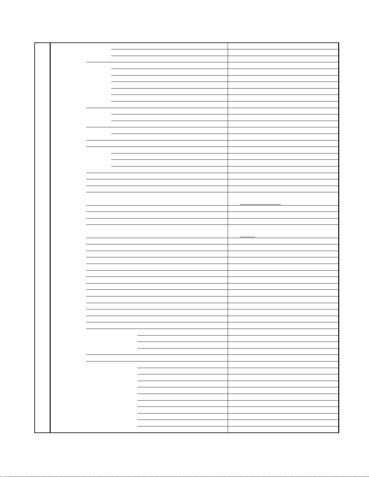
1. REMOVAL OF ANODE CAP
Read the following NOTED items before starting work.
*
After turning the power off there might still be a potential
voltage that is very dangerous. When removing the
Anode Cap, make sure to discharge the Anode Cap's
potential voltage.
*
Do not use pliers to loosen or tighten the Anode Cap
terminal, this may cause the spring to be damaged.
REMOVAL
1. Follow the steps as follows to discharge the Anode Cap.
(Refer to Fig. 1-1.)
Connect one end of an Alligator Clip to the metal part of a
flat-blade screwdriver and the other end to ground.
While holding the plastic part of the insulated Screwdriver,
touch the support of the Anode with the tip of the
Screwdriver.
A cracking noise will be heard as the voltage is discharged.
GND on the CRT
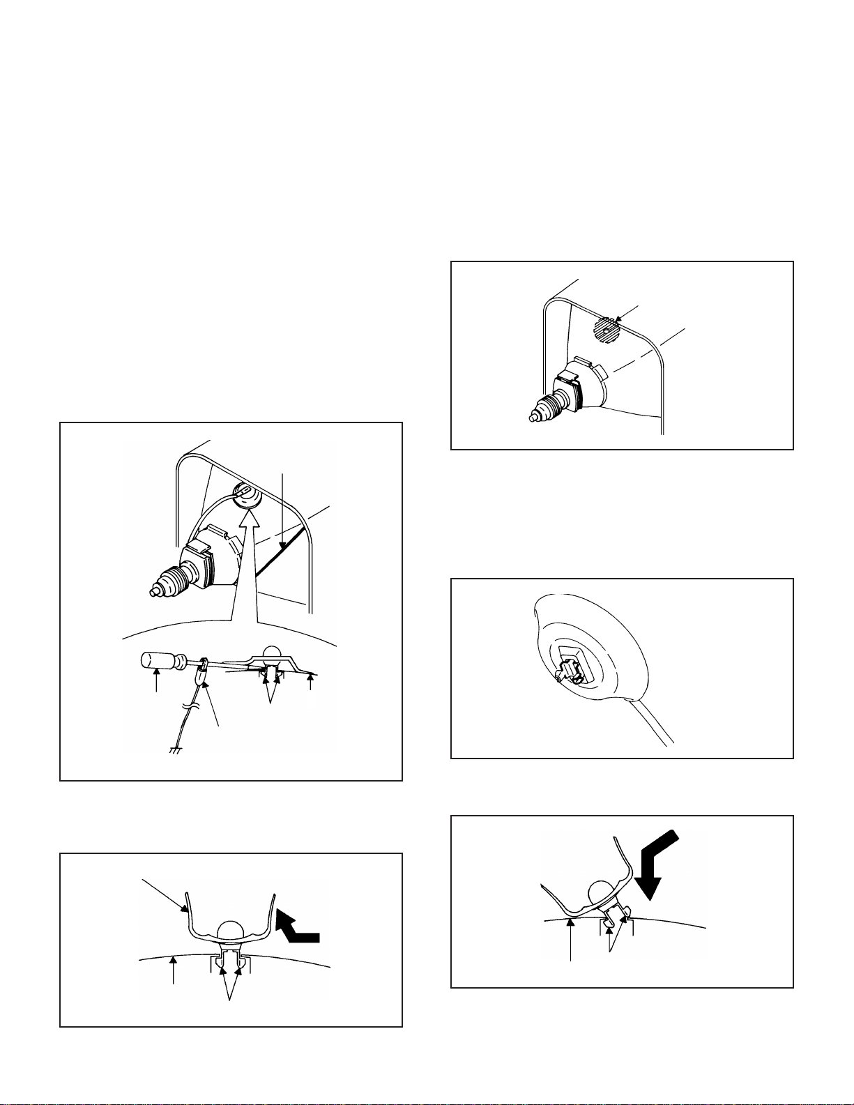
3. After one side is removed, pull in the opposite direction to
remove the other.
NOTE
Take care not to damage the Rubber Cap.
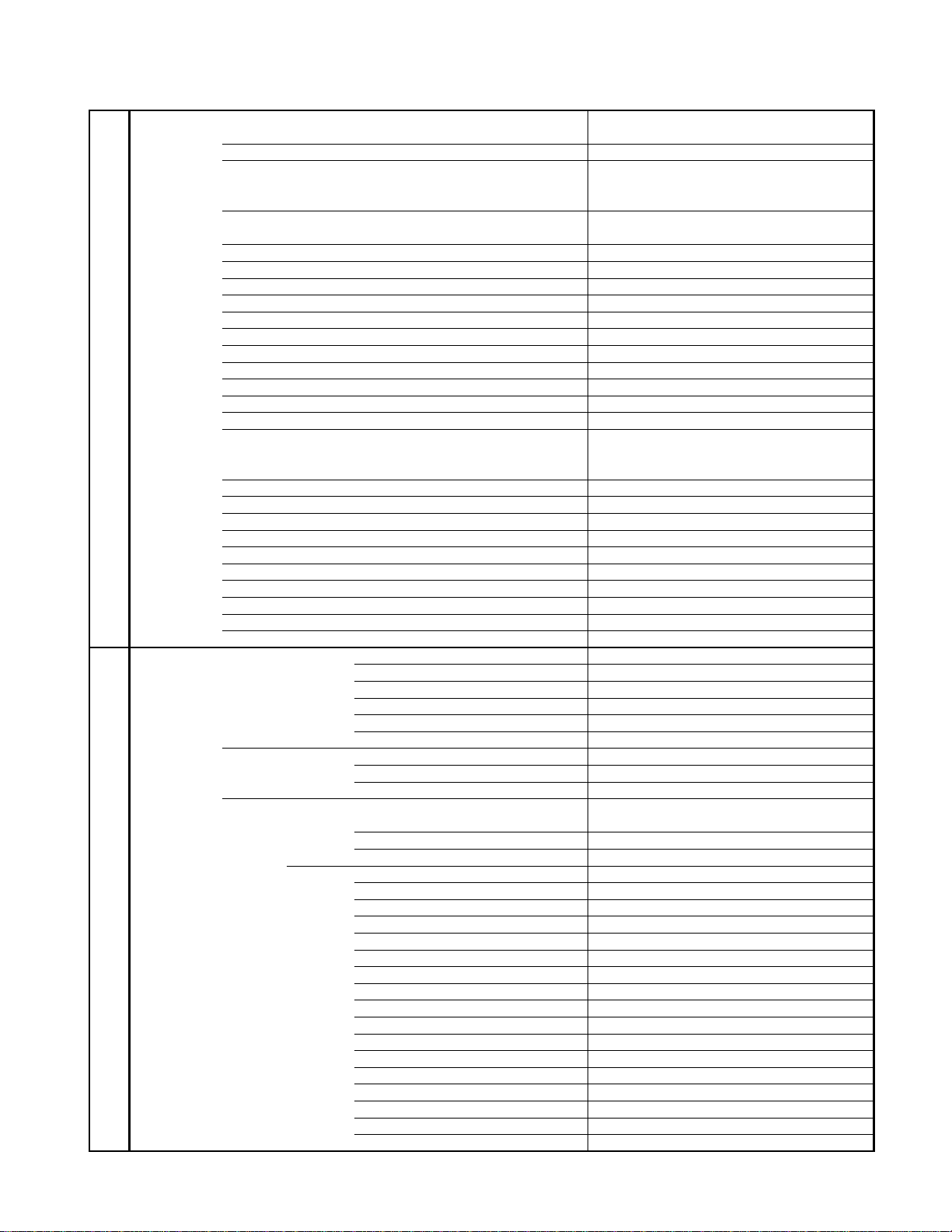
INSTALLATION
1. Clean the spot where the cap was located with a small
amount of alcohol. (Refer to Fig. 1-3.)
Location of Anode Cap
Fig. 1-3
NOTE
Confirm that there is no dirt, dust, etc. at the spot where
the cap was located.
2.3.Arrange the wire of the Anode Cap and make sure the
wire is not twisted.
Turn over the Rubber Cap. (Refer to Fig. 1-4.)
Screwdriver
Alligator Clip
GND on the CRT
Flip up the sides of the Rubber Cap in the direction of the
2.
arrow and remove one side of the support.
(Refer to Fig. 1-2.)
Rubber Cap
CRT
Support
Support
CRT
Fig. 1-1
Fig. 1-2
4. Insert one end of the Anode Support into the anode button,
then the other as shown in Fig. 1-5.
Support
CRT
5.6.Confirm that the Support is securely connected.
Put on the Rubber Cap without moving any parts.
B1-1
Fig. 1-4
Fig. 1-5
Page 11
DISASSEMBLY INSTRUCTIONS
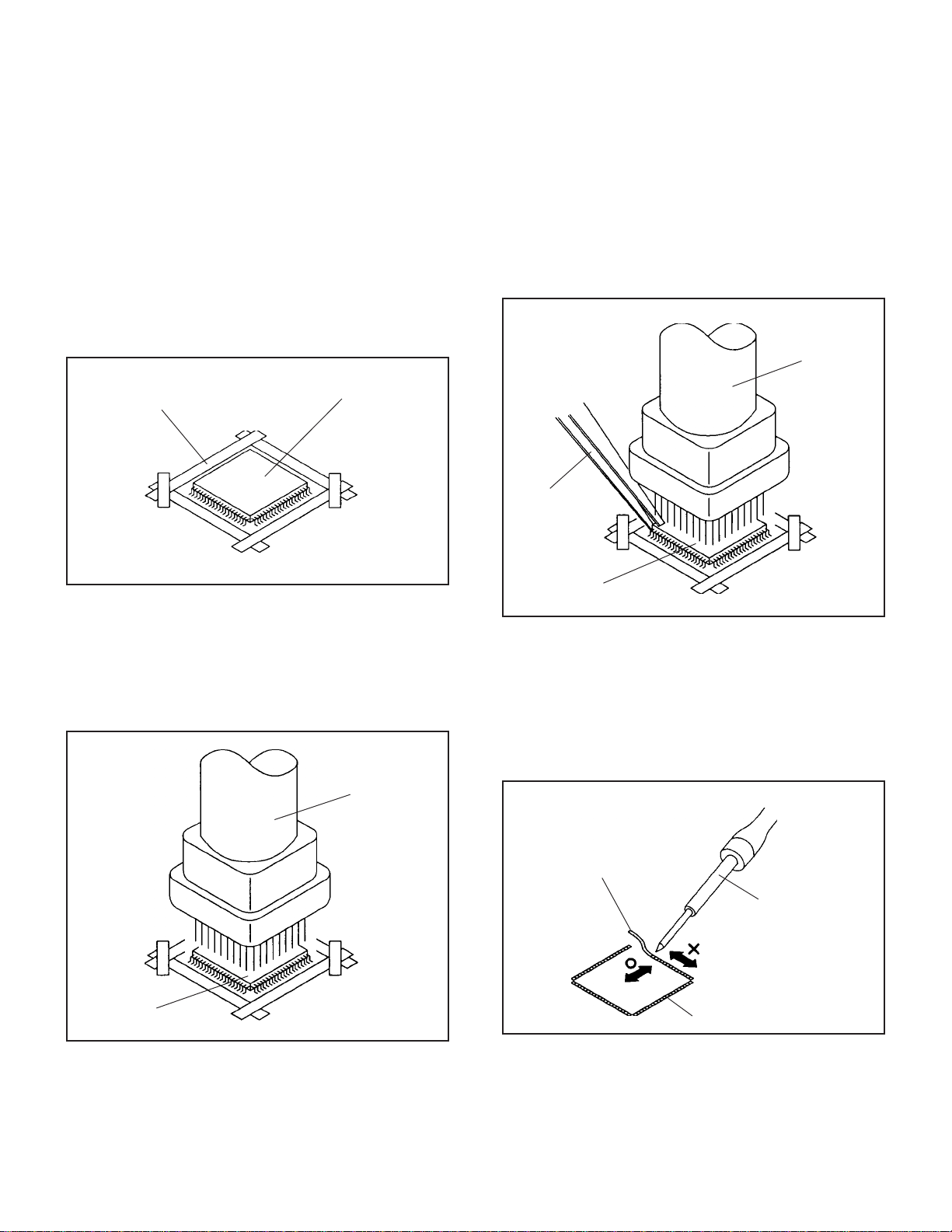
2.
REMOVAL AND INSTALLATION OF
FLAT PACKAGE IC
REMOVAL
Put the Masking Tape (cotton tape) around the Flat
1.
Package IC to protect other parts from any damage.
(Refer to Fig. 2-1.)
NOTE
Masking is carried out on all the parts located within 10
mm distance from IC leads.
When IC starts moving back and forth easily after
3.
desoldering completely, pickup the corner of the IC using a
tweezers and remove the IC by moving with the IC
desoldering machine. (Refer to Fig. 2-3.)
NOTE
Some ICs on the PCB are affixed with glue, so be
careful not to break or damage the foil of each IC leads
or solder lands under the IC when removing it.
Blower type IC
desoldering
machine
Masking Tape
(Cotton Tape)
Heat the IC leads using a blower type IC desoldering
2.
IC
machine. (Refer to Fig. 2-2.)
NOTE
Do not add the rotating and the back and forth
directions force on the IC, until IC can move back and
forth easily after desoldering the IC leads completely.
Blower type IC
desoldering machine
Fig. 2-1
Tweezers
IC
Peel off the Masking Tape.4.
Absorb the solder left on the pattern using the Braided
5.
Shield Wire. (Refer to Fig. 2-4.)
NOTE
Do not move the Braided Shield Wire in the vertical
direction towards the IC pattern.
Fig. 2-3
Braided Shield Wire
Soldering Iron
IC
Fig. 2-2
IC pattern
Fig. 2-4
B2-1
Page 12
DISASSEMBLY INSTRUCTIONS
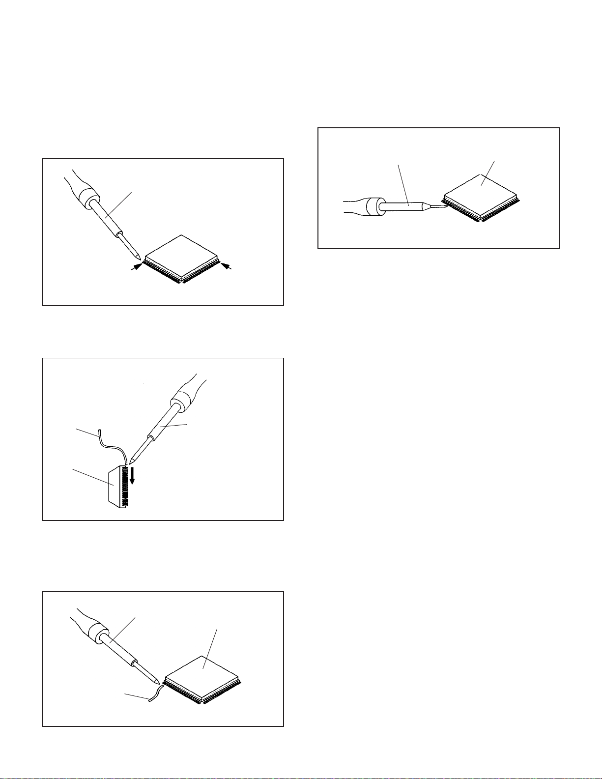
INSTALLATION
Take care of the polarity of new IC and then install the new
1.
IC fitting on the printed circuit pattern. Then solder each
lead on the diagonal positions of IC temporarily.
(Refer to Fig. 2-5.)
Soldering Iron
Solder temporarily
Supply the solder from the upper position of IC leads
2.
sliding to the lower position of the IC leads.
(Refer to Fig. 2-6.)
Solder temporarily
Fig. 2-5
When bridge-soldering between terminals and/or the
4.
soldering amount are not enough, resolder using a Thin-tip
Soldering Iron. (Refer to Fig. 2-8.)
Thin-tip Soldering Iron
IC
Fig. 2-8
Finally, confirm the soldering status on four sides of the IC
5.
using a magnifying glass.
Confirm that no abnormality is found on the soldering
position and installation position of the parts around the IC.
If some abnormality is found, correct by resoldering.
NOTE
When the IC leads are bent during soldering and/or
repairing, do not repair the bending of leads. If the
bending of leads are repaired, the pattern may be
damaged. So, always be sure to replace the IC in this
case.
Soldering IronSolder
IC
Supply soldering
from upper position
to lower position
Fig. 2-6
Absorb the solder left on the lead using the Braided Shield
3.
Wire. (Refer to Fig. 2-7.)
NOTE
Do not absorb the solder to excess.
Soldering Iron
IC
Braided Shield Wire
Fig. 2-7
B2-2
Page 13
SERVICE MODE LIST
This unit is provided with the following SERVICE MODES so you can repair, examine and adjust easily.
To enter to the SERVICE MODE function, press and hold both buttons simultaneously on the main unit or on the main unit
and on the remote control for more than a standard time in the appropriate condition. (See below chart.)
In case of the main unit and remote control, press the remote control buttons first, then press the main unit buttons.
Set
Condition
POWER ON
POWER ON
POWER ON
POWER ON
POWER ON
Set Key Operations
VOL. DOWN
(Minimum)
VOL. DOWN
(Minimum)
VOL. DOWN
(Minimum)
VOL. DOWN
(Minimum)
VOL. DOWN
(Minimum)
Remocon
Key
0 2 sec.
1 2 sec.
6 2 sec.
8
9 2 sec.
Standard
Time
2 sec.
Releasing of V-CHIP PASSWORD.
Initialization of factory TV data.
NOTE:
Can be checked of the INITIAL DATA of MEMORY IC.
Refer to the "WHEN REPLACING EEPROM (MEMORY) IC".
Check of the SUM DATA, MICON VERSION, POWER ON total hours
and Digital TV MICON Firmware on the screen.
Refer to the "WHEN REPLACING EEPROM (MEMORY) IC".
Display of the Adjustment MENU on the screen.
Refer to the "ELECTRICAL ADJUSTMENT" (On-Screen Display
Adjustment).
If you set factory initialization, the memories are reset such as
the channel setting, and the POWER ON total hours.
WHEN REPLACING EEPROM (MEMORY) IC
CONFIRMATION OF CHECK SUM, POWER ON TOTAL HOURS, MICON VERSION AND
DIGITAL TV MICON FIRMWARE VERSION
Initial total of MEMORY IC, POWER ON total hours, MICON VERSION and Digital TV MICON Firmware VERSION can be
checked on the screen. Total hours are displayed in 16 system of notation.
NOTE:
If you set a factory initialization, the total hours is reset to "0".
Please refer to "CONFIRMATION OF INITIAL DATA" when SUM DATA is not corresponding.
1.
Turn on the POWER, and set to the TV mode.
2.
Set the VOLUME to minimum.
3.
Press both VOL. DOWN button on the set and Channel button (8) on the remote control for more than 2 seconds.
4.
After the confirmation of each check sum, POWER ON total hours, Digital TV MICON Firmware and MICON VERSION,
turn off the power.
NOTE:
The each item value might be different according to each set.
ADDRESS DATA
CRT ON 0000
MICON Version
Digital TV MICON Firmware
Initial setting data check sum.
Rom correction data check sum.
OEC7174A_23
DTV CTT71222
INIT 26B2
ROM: 43EB
FIG. 1
C-1
POWER ON total hours.
= (16 x 16 x 16 x thousands digit value)
+ (16 x 16 x hundreds digit value)
+ (16 x tens digit value)
+ (ones digit value)
Page 14
WHEN REPLACING EEPROM (MEMORY) IC
If a service repair is undertaken where it has been required to change the MEMORY IC, the following steps should be taken to
ensure correct data settings while making reference to TABLE 1.
INIT +0 +1 +2 +3 +4 +5 +6 +7 +8 +9 +A +B +C +D +E +F
00 43 00 00 20 09 B 3 24 0D 4B 80 00 A 0 F A 00 00 00
10 00 00 00 65 4E 34 10 A1 00 00 00 00 60 00 10 8C
20 00 00 00 00 00 00 00 00 00 00 00 00 00 00 00 08
30 88 00 00 00 00 09 72 05 05 00 00 00 87 03 C 8 22
40 02 33 00 00 04 23 2D 20 00 40 20 40 40 40 00 00
50 00 64 00 00 00 00 00 00 0A 45 A0 00 FF 01 00 00
60 00 88 00 00 00 00 00 00 00 00 00 00 00 00 00 00
70 00 00 00 00 00 00 00 00 00 00 00 00 00 00 00 00
80 00 00 00 00 00 00 00 00 00 03 00 00 00 00 00 00
90 00 00 00 00 00 00 00 00 00 00 00 05 9D 01 00 84
A 0 04 11 00 00 00 05 00 01 00 00 00 05 12 13 05 82
B 0 01 00 00 00 00 04 00 04 00 02 00 00 00 00 00 00
C0 08 24 2F 33 37 38 39 3A 3B 3C 3C 3D 3F 40 40 41
D0 42 44 45 46 47 48 49 4A 4B 4C 4C 4D 4E 4F 50 50
E 0 51 52 53 53 54 54 55 55 57 58 5A 5B 5C 5D 5E 5F
F0 61 62 64 66 68 6E 73 78 7D 82 86 8A 8E 8E 8F 8F
Table 1
CONFIRMATION OF INITIAL DATA
1.
Enter DATA SET mode by setting VOLUME to minimum.
2.
Press both VOL. DOWN button on the set and Channel button (6) on the remote control for more than 2 seconds.
ADDRESS and DATA should appear as FIG 2.
3.
ADDRESS is now selected and should "blink". Using the CH. UP/DOWN button on the remote, step through the
ADDRESS until required ADDRESS to be changed is reached.
4.
Press VOL. UP/DOWN button to select DATA. When DATA is selected, it will "blink".
5.
Again, step through the DATA using CH. UP/DOWN button until required DATA value has been selected.
6.
Pressing VOL. UP/DOWN button will take you back to ADDRESS for further selection if necessary.
7.
Repeat steps 3 to 6 until all data has been checked.
8.
When satisfied correct DATA has been entered, turn POWER off (return to STANDBY MODE) to finish DATA input.
After the data input, set to the initializing of shipping.
9.
Turn on the Power.
10.
Set the VOLUME to minimum.
11.
Press both VOL. DOWN button on the set and Channel button (1) on the remote control for more than 2 seconds.
12.
After the finishing of the initializing of shipping, the unit will turn off automatically.
The unit will now have the correct DATA for the new MEMORY IC.
ADDRESS DATA
INIT 00 43
CRT ON 0000
OEC7174A_23
DTV CTT71222
INIT 26B2
ROM: 43EB
FIG. 2
C-2
Page 15
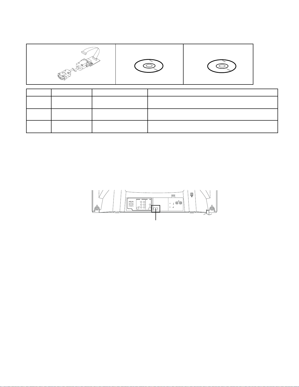
SERVICING FIXTURES AND TOOLS
Serial Communication
Change JIG
Ref. No.
JG205
JG206
Part No.
APJG205000
APJG206000
APJG176125JG176
JG206JG205
Parts Name
Serial Communication
Change JIG
Flash UP-Date Soft Disc
2007 SD DTV Rom Disc
Flash UP-Date Soft Disc
JG176
Connect the set to personal computer
Up-Date of the Firmware
Up-Date of the DIGITAL Firmware
2007 SD DTV Rom Disc
Remarks
RE-WRITE FOR DIGITAL SOFT FIRMWARE
Confirm that the AC cord is plugged out.
1.
Using the Serial Communication Change JIG (JG205), connect the set to personal computer. (Refer to Fig. 1)
2.
NOTE: It is possible to write only with the personal computer of WINDOWS.
Fig. 1
3.
Using the Flash UP-Date Soft Disc (JG206) and USA SD DTV ROM DISC (JG176), please Re-write the DIGITAL SOFT
FIRMWARE.
The operating manual for Re-writing is included in Flash UP-Date Soft Disc (JG206).
C-3
Page 16

ELECTRICAL ADJUSTMENTS
1. ADJUSTMENT PROCEDURE
Read and perform these adjustments when repairing the
circuits or replacing electrical parts or PCB assemblies.
CAUTION
•
Use an isolation transformer when performing any service
on this chassis.
•
Before removing the anode cap, discharge electricity
because it contains high voltage.
•
When removing a PCB or related component, after
unfastening or changing a wire, be sure to put the wire
back in its original position.
•
When you exchange IC and Transistor with a heat sink,
apply silicon grease on the contact section of the heat
sink. Before applying new silicon grease, remove all the
old silicon grease. (Old grease may cause damages to the
IC and Transistor.)
Prepare the following measurement tools for electrical
adjustments.
1. Oscilloscope
2. Digital Voltmeter
3. Multi-sound Generator
4. Pattern Generator
On-Screen Display Adjustment
1. In the condition of NO indication on the screen.
Press the VOL. DOWN button on the set and the Channel
button (9) on the remote control for more than 2 seconds
to appear the adjustment mode on the screen as shown in
Fig. 1-1.
TV-A
4:3
00 OSD H
2.
Use the Channel UP/DOWN button or Channel button
(0-9) on the remote control to select the options shown
in Fig. 1-2.
3.
Press the MENU button on the remote control to end the
adjustments.
4.
To display the adjustment screen for TV-A, TV-D, AV
and YUV mode, press the INPUT button on the remote
control. Press the VOL.DOWN button on the set and
the channel (9) on the remote control for more than 2
seconds.
20
Fig. 1-1
FUNCTION
NO.
00
01
02
03
04
05
06
07
08
09
10
11
12
13
14
15
16
29
30
31
OSD H
OSD C
CUT OFF
H.POSI
H BLK L
H BLK R
V. SIZE
V. POSI
V. LIN
VS CORR
V COMP
R.BIAS
G.BIAS
B.BIAS
R.DRV
G.DRV
B.DRV
BRI.CENT
BRI.MAX
BRI.MIN
NO.
FUNCTION
32
CONT.CENT
33
CONT.MAX
34
CONT.MIN
35
COL.CENT
36
COL.MAX
37
COL.MIN
38
TINT CENT
39
SHARP.CENT
40
SHARP.MAX
41
SHARP.MIN
42
SUB BIAS
43
H.SIZE
44
PARABOLA
45
TRAPEZIUM
46
COR TOP
47
COR BTM
48
TEST STEREO
49
X-RAY
Fig. 1-2
2. BASIC ADJUSTMENTS
2-1: CONSTANT VOLTAGE
1.
Place the set in AV MODE without signal.
2.
Connect the digital voltmeter to the TP003.
3.
Adjust the VR502 until the digital voltmeter is 130 ± 0.5V.
2-2: CUT OFF
1.
Place the set in Aging Test for more than 15 minutes.
2.
Place the set in AV MODE without signal.
3.
Using the remote control, set the brightness and
contrast to normal position.
4.
Activate the adjustment mode display of Fig. 1-1 and
press the channel button (02) on the remote control to
select “CUT OFF”.
5.
Adjust the Screen V olume until a dim raster is obtained.
2-3: WHITE BALANCE
NOTE: Adjust after performing CUT OFF adjustment.
Place the set in Aging Test for more than 15 minutes.
1.
Receive the white 100% signal from the Pattern
2.
Generator.
Using the adjustment control, set the brightness and
3.
contrast to normal position.
Activate the adjustment mode display of Fig. 1-1 and
4.
press the channel button (11) on the remote control to
select "R.BIAS".
Using the VOL. UP/DOWN button on the remote control,
5.
adjust the R.BIAS.
Press the CH. UP/DOWN button on the remote control to
6.
select the "R.DRIVE", "B.DRIVE", "G.BIAS" or "B.BIAS".
Using the VOL. UP/DOWN button on the remote control,
7.
adjust the R.DRIVE, B.DRIVE, G.BIAS or B.BIAS.
Perform the above adjustments 6 and 7 until the white
8.
color is achieved.
2-4: FOCUS
1.
Receive the monoscope pattern.
2.
Turn the Focus Volume fully counterclockwise once.
3.
Adjust the Focus V olume until picture is distinct.
D-1
Page 17

ELECTRICAL ADJUSTMENTS
2-5: BRIGHT CENT
1.
Receive the monoscope pattern. (RF Input)
2.
Set the screen mode to FULL.
3.
Using the remote control, set the brightness and contrast
to normal position.
4.
Activate the adjustment mode display of Fig. 1-1 and
press the channel button (29) on the remote control to
select "BRI. CENT".
5.
Press the VOL. UP/DOWN button on the remote control
until the white 10% is starting to be visible.
6.
Receive the monoscope pattern. (Audio Video Input)
7.
Press the INPUT button on the remote control to set to
the AV mode. Then perform the above adjustments 2~5.
8.
Receive the monoscope pattern.
9.
Press the INPUT button on the remote control to set to
the YUV mode.Then perform the above adjustments 2~5.
2-6: CONTRAST MAX
1.
Receive an over 70dB color bar pattern. (RF Input)
2.
Using the remote control, set the brightness and
contrast to normal position.
3.
Activate the adjustment mode display of Fig. 1-1 and
press the channel button (33) on the remote control
to select "CONT.MAX".
4.
Press the VOL. UP/DOWN button on the remote
control until the contrast step No. becomes "70".
5.
Receive a broadcast and check if the picture is normal.
6.
Receive the color bar pattern. (Audio Video Input)
7.
Press the INPUT button on the remote control to
set to the AV mode. Then perform the above
adjustments 2~5.
8.
Receive the monoscope pattern.
9.
Press the INPUT button on the remote control to set to the
YUV mode.Then perform the above adjustments 2~5.
A
Fig. 2-1
2-8: COLOR CENT
Receive the color bar pattern. (RF Input)
1.
Using the remote control, set the brightness, contrast, color
2.
and tint to normal position.
Connect the oscilloscope to TP022.
3.
Activate the adjustment mode display of Fig. 1-1 and
4.
press the channel button (35) on the remote control to
select "COL.CENT".
Adjust the VOLTS RANGE VARIABLE knob of the
5.
oscilloscope until the range between white 100% and 0%
is set to 4 scales on the screen of the oscilloscope.
Press the VOL. UP/DOWN button on the remote control
6.
until the red color level is adjusted to 110 ± 10% of the
white level. (Refer to Fig. 2-2)
Receive the video color bar pattern. (Audio Video Input)
7.
Press the INPUT button on the remote control to
8.
set to the AV mode. Then perform the above
adjustments 2~6.
Receive the video color bar pattern.
9.
Press the INPUT button on the remote control to set to the
10.
YUV mode.Then perform the above adjustments 2~6.
Receive the video color bar pattern.
11.
Press the INPUT button on the remote control to set to the
12.
DIGITAL mode.Then perform the above adjustments 2~6.
2-7: TINT
1.
Receive the color bar pattern. (RF Input)
2.
Using the remote control, set the brightness, contrast
and tint to normal position.
3.
Connect the oscilloscope to TP024.
4.
Activate the adjustment mode display of Fig. 1-1 and
press the channel button (38) on the remote control to
select "TINT".
5.
Press the VOL. UP/DOWN button on the remote control
until the section A becomes as straight line.
(Refer to Fig. 2-1)
6.
Receive the monoscope pattern. (Audio Video Input)
7.
Press the INPUT button on the remote control to set to
the AV mode. Then perform the above adjustments 2~5.
8.
Receive the monoscope pattern.
9.
Press the INPUT button on the remote control to set to
the YUV mode.Then perform the above adjustments 2~5.
10.
Receive the monoscope pattern.
11.
Press the INPUT button on the remote control to set to
the DIGITAL mode.Then perform the above adjustments
2~5.
white 100%
2-9: HORIZONTAL POSITION
1.
Receive the monoscope pattern.
2.
Using the remote control, set the brightness and contrast
to normal position.
3.
Activate the adjustment mode display of Fig. 1-1 and
press the channel button (03) on the remote control to
select “H.POSI”.
4.
Press the VOL. UP/DOWN button on the remote control
until the SHIFT quantity of the OVER SCAN on right and
left becomes minimum.
D-2
110%
Fig. 2-2
Page 18

ELECTRICAL ADJUSTMENTS
2-10: HORIZONTAL SIZE
1.
Receive the monoscope pattern.
2.
Using the remote control, set the brightness and
contrast to normal position.
3.
Activate the adjustment mode display of Fig. 1-1 and
press the channel button (43) on the remote control to
select "H.SIZE".
4.
Press the VOL. UP/DOWN button on the remote control
until the SHIFT quantity of the OVER SCAN on the right
and left becomes 10± 3%.
2-14: TRAPEZIUM
1.
Receive the crosshatch signal from the Pattern Generator.
2.
Using the remote control, set the brightness and contrast
to normal position.
3.
Activate the adjustment mode display of Fig. 1-1 and
press the channel button (45) on the remote control to
select “TRAPEZIUM”.
4.
Press the VOL. UP/DOWN button on the remote control
until the both ends right and left vertical lines of the 1th
length lines screen become parallel.
2-11: VERTICAL LINEARITY
Receive the monoscope pattern.
1.
Using the remote control, set the brightness, contrast,
2.
to normal position.
Activate the adjustment mode display of Fig. 1-1 and
3.
press the channel button (08) on the remote control to
select "V.LIN".
Press the VOL. UP/DOWN button on the remote control
4.
until the SHIFT quantity of the OVER SCAN on upside
and downside becomes minimum.
2-12: VER TICAL POSITION
1.
Receive the monoscope pattern.
2.
Using the remote control, set the brightness and contrast
to normal position.
3.
Adjust the VR401 until the horizontal line becomes fit to
the notch of the shadow mask.
(Refer to Fig. 2-3)
horizontal line
Notch
2-15: PALABOLA CORR
1.
Receive the chosshatch pattern.
2.
Using the remote control, set the brightness and
contrast to normal position.
3.
Activate the adjustment mode display of Fig. 1-1 and
press the channel button (44) on the remote control to
select “PALABOLA”.
4.
Press the VOL. UP/DOWN button on the remote control,
so that the line becomes straight from the outside of
the right and left.
2-16: COR TOP/BTM
1.
Receive the crosshatch signal from the Pattern Generator.
2.
Set the screen mode to FULL.
3.
Using the remote control, set the brightness and contrast
to normal position.
4.
Activate the adjustment mode display of Fig. 1-1 and
press the channel button (46) on the remote control to
select “COR. TOP”.
5.
Press the VOL. UP/DOWN button on the remote control
until the both ends vertical lines become straight.
6.
Activate the adjustment mode display of Fig. 1-1 and
press the channel button (47) on the remote control to
select “COR. BTM”.
7.
Press the VOL. UP/DOWN button on the remote control
until the both ends vertical lines of the screen become
parallel.
Shadow mask
Fig. 2-3
2-13: VER TICAL SIZE
1.
Receive the monoscope pattern.
1
2
2.
Using the remote control, set the brightness and contrast
to normal position.
3.
Activate the adjustment mode display of Fig. 1-1 and
press the channel button (06) on the remote control to
select “V. SIZE”.
4.
Press the VOL. UP/DOWN button on the remote control
until the SHIFT quantity of the OVER SCAN on upside
and downside becomes 9 ± 2%.
D-3
Page 19

ELECTRICAL ADJUSTMENTS
2-17: OSD POSITION
1.
Receive the monoscope pattern from the Pattern
Generator.
2.
Using the remote control, set the brightness and
contrast to normal position.
3.
Activate the adjustment mode display of Fig. 1-1 and
press the channel button (00) on the remote control to
select "OSD H".
4.
Press the VOL. UP/DOWN button on the remote control
until the difference of A and B becomes minimum.
(Refer to Fig. 2-4)
TV-A
4:3
00 OSD H
20
2-18: Confirmation of Fixed Value (Step No.)
Please check if the fixed values of each of the adjustment
item is set correctly referring below.
FUNCTION
NO.
OSD C
01
H BLK L
04
H BLK R
05
V.POSI
07
VS CORR
09
V COMP
10
BRI.MAX
30
BRI.MIN
31
CONT.CENT
32
CONT.MIN
33
COL.MAX
36
COL.MIN
37
SHARP.CENT
39
SHARP.MAX
40
SHARP.MIN
41
SUB BIAS
42
TEST STEREO
48
ANALOG
TV-A
02
05
02
01
11
00
90
50
55
30
120
20
27
63
00
00
00
DIGITAL
TV-D
02
05
02
01
11
00
90
50
50
30
120
20
25
63
00
00
00
VIDEO1, VIDEO2
AV
02
05
02
01
11
00
90
50
50
30
120
20
25
63
00
00
00
Colorstream
YUV
02
05
02
01
11
00
90
50
50
50
120
20
25
63
00
00
00
A
B
Fig. 2-4
D-4
Page 20

ELECTRICAL ADJUSTMENTS
3. PURITY AND CONVERGENCE
ADJUSTMENTS
NOTE
1.
Turn the unit on and let it warm up for at least 30
minutes before performing the following adjustments.
2.
Place the CRT surface facing east or west to reduce the
terrestrial magnetism.
3.
Turn ON the unit and demagnetize with a Degauss Coil.
3-1: STATIC CONVERGENCE (ROUGH ADJUSTMENT)
1.
Tighten the screw for the magnet. Refer to the adjusted
CRT for the position. (Refer to Fig. 3-1)
If the deflection yoke and magnet are in one body,
untighten the screw for the body.
2.
Receive the green raster pattern from the color bar
generator.
3.
Slide the deflection yoke until it touches the funnel side
of the CRT.
4.
Adjust center of screen to green, with red and blue on
the sides, using the pair of purity magnets.
5.
Switch the color bar generator from the green raster
pattern to the crosshatch pattern.
6.
Combine red and blue of the 3 color crosshatch
pattern on the center of the screen by adjusting the pair
of 4 pole magnets.
7.
Combine red/blue (magenta) and green by adjusting the
pair of 6 pole magnets.
8.
Adjust the crosshatch pattern to change to white by
repeating steps 6 and 7.
3-2: PURITY
NOTE
Adjust after performing adjustments in section 3-1.
1.
Receive the green raster pattern from color bar generator.
2.
Adjust the pair of purity magnets to center the color on
the screen.
Adjust the pair of purity magnets so the color at the ends
are equally wide.
3.
Move the deflection yoke backward (to neck side)
slowly, and stop it at the position when the whole screen
is green.
4.
Confirm red and blue color.
5.
Adjust the slant of the deflection yoke while watching the
screen, then tighten the fixing screw.
DEFLECTION Y OKE
DEFLECTION Y OKE SCREW
MAGNET SCREW
3-3: STATIC CONVERGENCE
NOTE
Adjust after performing adjustments in section 3-2.
1.
Receive the crosshatch pattern from the color bar
generator.
2.
Combine red and blue of the 3 color crosshatch
pattern on the center of the screen by adjusting the pair
of 4 pole magnets.
3.
Combine red/blue (magenta) and green by adjusting the
pair of 6 pole magnets.
3-4: DYNAMIC CONVERGENCE
NOTE
Adjust after performing adjustments in section 3-3.
1.2.Adjust the differences around the screen by moving the
deflection yoke upward/downward and right/left.
(Refer to Fig. 3-2-a)
Insert three wedges between the deflection yoke and
CRT funnel to fix the deflection yoke.
(Refer to Fig. 3-2-b)
R G B
R
G
B
UPWARD/DOWNWARD SLANT RIGHT/LEFT SLANT
WEDGE WEDGE
WEDGE POSITION
R
G
B
Fig. 3-2-a
WEDGE
Fig. 3-2-b
R G B
PURITY MAGNETS
6 POLE MAGNETS
4 POLE MAGNETS
Fig. 3-1
D-5
Page 21

ELECTRICAL ADJUSTMENTS
DIGITAL PCB
C
P
8
0
7
C
R
T
TU001
4. ELECTRICAL ADJUSTMENT PARTS LOCATION GUIDE (WIRING CONNECTION)
TP003
W002
FB401
VR502
CRT
CP801A
CRT PCB
CD803
CP401
CP803
J801
CP101
CP806
CP802B
CD801
J703 J704 J701
SPEAKER
VR401
CRT
TP024
TP022
CP801B
R805
R803
CP1001
CD802
J702
CD1001
DEGAUSS COIL
L503
AC IN
CD501
S501
S502
CP502
OS101
CP802A
J709 J710 J711
TV MT PCB
D-6
Page 22

FRONT -VIDEO
OUT
J709
YUV_IN
J704
S-JACK
J702
AV1_IN
J701
FRONT-AUDIO.L
J710
FRONT-AUDIO.R
J711
AUDIO OUT
J703
2
5
2
3
3
4
6
4
2
2
2
3
2
UN_REG. 12V
AV SW IC
IC703 NJM2534V(TE2)
1
3
5
7
SOUND AMP IC
IC1001 AN17822A
2
6
8
4
10
12
REG.+3.3V IC
IC002 BA00BC0WFP-E2
1
2
4
REG.1.8V IC
IC004 LA5779-E
2
1
4
REG.+2.6V IC
IC003 BA00BC0WFP
1
2
4
X601
3.579545MHz
AV SW IC
IC702 NJM2534V(TE2)
1
3
7
SPEAKER L
SP1001
SPEAKER R
SP1002
5
UN_REG. 6V
MICON/CHROMA BLOCK DIAGRAM
CHROMA IC
IC601 LA76327M-MPB-E
35
XTAL 3.58
VIDEO IN2
9
30
Y IN
29 V IN
U IN
28
S.VIDEO Y
44
S.VIDEO C
40
VIDEO IN1
1
COMB C
5
COMB Y
3
CVBS
41
TU001
15
B OUT
G OUT
R OUT
V OUT
H OUT
OSD_R
OSD_G
OSD_B
OSD BLK1
TUNER CVBS
MEMORY IC
IC199
AT24C08AN-10SU-2.7
SDA
SCL
12
13
20
18
VD
HD
SCL1
SDA1
5
6
16
15
14
19
23
57
56
55
54
60
59
50
51
42
1619
Q802, Q806
BLUE OUT
Q801, Q804
RED OUT
Q402
H.DRIVE
Q803, Q805
GREEN OUT
Q405
H.OUT
OSD_R
62
OSD_G
63
OSD_B
62
OUT1
60
59
V_SYNC
58
H/C_SYNC
SCL1
71
72
SDA1
26
DTV_P.ON_H
89
MESSERGE_
REG._IN
31 DTV_RESET
21
TUNER DIGITAL-L
J801
11
6
8
MICON
IC101 OEC7174A
F
7
REMOCON
X.IN
X.OUT
KEY A
KEY B
RESET
P.CON+9V
FB401
F
S
V-OUT IC
IC401 LA7847-E
5
14
35
36
9
10
X102
32.768KHz
SYSTEM RESET
IC102 PST3245NR
34
86IIC_OFF
AT+5V_D
HV
1
CRT
V801
2
OS101
1
DY
POWER
VOL DOWN
CH DOWN
VOL UP
CH UP
1
MICON_DATA
CP101
RESET
DTV_TX
DTV_RX
IIC_OFF
SDA
SCL
+3.3v
CVBS_IN/740_INIT
SD_H/SEL_SW
NC
NC
SIF/2ND_CVBS
NC
DTV_RESET
I2C_DATA
TV BLOCK
CP2403
IF_N
IF_P
IF_AGC
AFT1
SPDIF
+9V
AUDIO-R
AUDIO-L
Pb OUT
Y OUT
Pr OUT
I2C_CLK
TX
RX
8
6
5
4
3
2
7
28
27
25
24
22
21
20
19
18
17
16
15
14
13
12
11
10
9
8
+3.3V 7
+5V
+2.6V
6
5
2
1
AFT0/MSG_REG
ASIC+1.8V
E-1
E-2
Page 23

SD DIGITAL MODULE BLOCK DIAGRAM
U9
U10
A8
C12
C11
U13
PB OUT
Y OUT
RESETN
I2C_DATA
MSG_REQ
+3.3V
ASIC+1.8V
T3R3R2
R1
SDIN
BCLK
LRCK
ACLK
+5V
CVBS_IN/740_INIT
28
SD_H/SEL_SW27IF_N
25
IF_P
24
IF_AGC
22
AFT121
SPDIF20+9V
19
AUDIO-R
18
AUDIO-L
17
SIF/2ND_CVBS
16
Pb OUT
15
Y OUT
14
Pr OUT
13
DTV_RESET
12
I2C_CLK11I2C_DATA
10
TX
9
RX
8
7
AFT0/MSG_REQ
6
ASIC+1.8V
5
+5V2
+2.6V
1
TV BLOCK
CP2403
B11
B12
SDA
SCL
+3.3V
+3.3V
NC
I2C_CLK
SIF AMP
SIF
SIF
F3
IF_AGC
A5
IF_P
B1
IF_N
C1
SD_H/SEL_SW
U5
CVBS_IN/740_INIT
F1
+3.3V
NC
NC
NC
NC
NC
X2401
25MHz
SPI FLASH
IC2405
EN25P16-50HCP
2
5 6
8
1
3
7
C5
A3
C6
A4
C4
B4
5 6
EEPROM
IC2403
AT24C04N-10SU-2.7
8
DTV ASIC
IC2401
ZR39740HGCF-B0
10 7
2 3 4
1
AUDIO DAC
IC2406
CS4345-CZZ
9
ADR
DAT
13
16
+2.6V
256Mbit DDR SDSAM
IC2402
HY5DU561622ETP-D43
+2.6V
E-3
E-4
Page 24

W040
W870
D003
C717
C714
C
1005_
1
C023
C022
CP2403B
W125
R018
W115
C104
R132
R
4
5
2
C502
CP502
R500
C527
C501_1
C408
D
4
0
9
C426
R527
R502
R410
D
5
1
0
C521
C507_2
R
0
0
2
CP507
CP508
D522
D526
CP509
C513
C519
C
5
3
5
R438_1
C403
C406
C423
C512
C514
C515
C522
C534_1
D402
D403
D406
D414
D415
D507
D516
D520
D521
D523
D525
D530
D532
FH501
R406
R413
R416
R418
R420
R422
R426
R427
R428
R437
R443
R503
R519
R520
R535
R539
R540
R544
R554
R553
W003
W004
W005
W007
W018
W019
W022
W016
W822
R513
D407
R414
R432
B501_1
R
4
2
1
C432
W823
R
4
1
1
C421
T
H
5
0
1
D528
D535
R510
R547
D514
C509
R552
C554
C549
IC504
D524
D509
C510
Q502
H
S
5
0
1
TP004
W020
W015
R401
C
5
1
7
C418_1
C005
L402_1
R439
B401
C
4
1
2
C420
L502
D531
D527
C118
W067
J711
R746
R745
W874
W095
W164
C603
C609
C612
C624
C635
C638
D611
L602
R604
R616
R618
R627
X601
W814
R
6
0
3
D612
R619
R622
C611
W157
C648
C649
C442
R
6
5
0
L601
D408
C433 R524
W128
R005
C427_1
C518
S502S501
C010
CP501
W829
W839
W006
W111
W841
C002
C613
W145
W146
R549
R537
R122
R118
R019
C101
C105
C106
W107
W835
W091
C115
C119
C123
W086
W094
W171
W167
X102
R130
W168
W034
W142
C017
R021
W853
W810
W127W110
W109
W108
W148
W149
W150
W112
TU001
W159
W158
C
8
0
2
C801
R802
D803
J
8
0
1
W116
W117
W165
W081
W163
W172
W817
W845
W088
W106
W803
D539
W021
R528
W126
R407_1
C026
W090
W129
W037
W036
W162
C
P
8
0
7
W076
W027
W143
W848
W849
W113
C436
C034
W056
W070
W153
W044
C012
W842
W087
W078
W080
W077
W074
W075
W045
W071
W072
W174
W173
R605
C650
W183
W182
C656
C653
W863
R041_1
W144
C413
C053
W147
D504
D501
D503
W824
W880
W826
W850
CD501
W857
C651
B005
W886
C437
C102_3
W042
C054
R036
SERVICEFOR INFORMATIONABOUTCRITICAL
COMPONENTSSEEINSIDEBACKCOVER.
CAUTION
,
ATTENTION
INFORMATIONPOURSERVICEDES
PIECE CRITIQUE VOIRAUVERSO.,
PRINTED CIRCUIT BOARDS
TV MT/CRT (INSERTED PARTS)
SOLDER SIDE
F-1
CP801A
Q507
CP801B
R120
R134
R408
VR502
Q804
R506
D812
D109
D404
FB401
W002
R543
T501_1
C541
Q504
R504
R508
OS101
R530
C537
D508
R529
R545
RY501
C506
C524
Q514
R541
F501
D517
D506
C505
L501
FH502
- REPLACE AS MARKED.
RISK OF FIRE
SW105
L801
Q802
Q806
R807
R803
R805
C508
R542
R521
R501
C503
CP401
Q405
Q503
R434
D515
CP803
R804
R505
W008
D529
R824
SW102
R507
C504
Q505
R546
D811
D405
HS402
CP802B
W009
Q803
CCF076A
CP806
D511
C516
D512
D802
R806
B504
C520
Q801
Q805
D505
D810
D801
TP023
TP022
TP024
R430
TP003
W001
D502
W100
W033
W047
R640
Q611
J704J701
C430
W065
W102
R006
R004
C1011
W059
W063
Q501
S826X
J710
Q003
W060
R1016
W082
W051
W049
W048
R522
W180
W079
W179
W878
W054
W066
W884
W043
D533
W046
W073
W050
W057
L006
C715
J709
W011
W052
W175
W176
W177
W013
W012
W178
C401
J703
W882
W883
W808
W855
W862
Q402
HS001
W032
C407
W031
IC004
W024
W023
W030
L007
W026
W025
R441
VR401
W029
W028
SW103
CP101
D411
R515
T401
D410
B405
SW104
C417
D513
R459
W836
R526
R525
W890
W820
L403
C422_1
D416
D401
IC401
C539
R536
D519
Q512
W856
SW101
D412
W889
C405
C402
Q509
R512
Q508
W139
L004
W166
W136
J702
R613
CP802A
W818
W131
R141
R629
W084
W812
R601
R636
C733
W124
W123
W122
W133
Q602
C632
R645
R606
W156
W039
R612
S826Y
Q607
W035
W137
W135
Q603
D104
S829X
S829Y
W134
W041
W096
W093
C015
W181
R110
R108
C120
X101
L101
CP1001
W064
W062
W061
W058
W101
W838
W038
W083
IC1001
C1006
W098
W089
W085
W821
CMF094A
W104
W103
L001
W881
W119
W118
Q609
W140
W138
W161
W184
W873
W141
R648
W053
W055
R632
R623
Q608
C622
F-2
Page 25

R710
R1003
C709_1
C708_1
R1001
R1002
R1015
R1014
R1017
C1007
R1008
R1006
C1003
C1001
C1004
C1002
R013
R012
R011
C006
C025
C021
R028
R026
R736
C734
R739
C716
R717
C736
R726
R714
C725
R735
C722
R730
R114
C143
R106
R113
R412
C404
R417
R415
R511
R518
R509
R444
C424
C416
R404
R425
R405
R431
R548
C511
R532
R533
R442
R133
C741
C742
R743
C719
C103
R162
R653
C606
C634
R609
R610
R611
C614 C617
C601
C621
R615
C618
C619
R624
C627
C626
C630
C629
C628
R625
C644
C645
C646
R607
R660
R617
IC601
R176
R630
R659
R608
C011
C029
C041
R009
R010
C003
C042 C043
C046
C020
C009
C008 C016
C018
R123
R119
R107
R020
R138
C135
C136
R135
R101
C140
R140
C109
R116
R117
R121
R126
C111
C107
C108
C121
R129
C127
C124
R017
R159
C131
C130
C133
C134
C138
C137
C126
R189
R186
R111
C146
C142
C132
C129
C122
R109
R812
R821
R820
C806
R816
R809
R813
R811
R815
C810
C811
C809
R808
R801
R819
R818
R817
B003
B002
B001
R124
C033
D001
R040
R128
C116
IC101
C139
C148
C147
C038
R641
R142
R143
R144
C636
C647
C149
C040
C049 C050
C051
B004
C604
C052
C410
C608
C654
C657
R007
R178
R654
C150
R652
PRINTED CIRCUIT BOARDS
TV MT/CRT (CHIP MOUNTED PARTS)
SOLDER SIDE
Q105
CCF076A
R810
R814
R127
Q506 Q510
51
CMF094A
R131
R136
31
IC102
R125
R102
R104
IC199
R030
Q106
R039
R038
81
Q612
1
R656
R638
R175
C720
Q104
49
1
17
R115
R744
Q108
Q610
Q605
33
R635
Q604
Q601
R626
R516
Q1001
R711
IC002
Q002
R003
IC702
IC703
R027
Q007
R1010
IC003
R733
Q005
Q006
Q001
R016
R015
F-3
F-4
Page 26

B2419
C2441
C2442
C2443
B2418
B2417
C2444
IC2406
R2437
R2436
C2480
L2401
C
2
4
7
6
R2448
B2404
C2404
R2417
R2429
C2478
NR2409
C2536
C2537
C2541
R2484
C2565
R2478
C2552
C2530
R2462
C2549
L2421_1
L2422_1
C2473
C2472
IC2401
C2462
C2465
C2460
C2466
C2461
C2464
C2410
C2463
C2467
C2540
C2544
C2548
C2550
R2423
R2424
R2505
C2543
R2516
R2504
R2422
R2421
C2437
C2457
C2453
C2436
C2406
C2447
C2412
C2449
C2433
C2452
C2434
C2451
C2435
R2435
R2434
NR2408
B2407
B2408
B2409
B2410
B2413
B2414
B2415
C2499
C2500
C2501
C2502
C2505
C2506
C2507
C2415
C2416
C2417
C2519
R2487
R2489
R2486
R2485
C2569
R2451
C2553
B2405
C2405
C2411
C2409
B2403
C2403
C2402
R2420
B2402
C2408
C2483
C2484
C2485
C2488
C2489
C2490
R2412
NR2401
NR2403
NR2402
R2413
R2408 R2407
R2473
C2418
C2419
C2438
C2512
C2513
C2514
C2520
C2546
C2568
C2571
R2499
R2496
R2515
R2512
R2519
IC2405
PRINTED CIRCUIT BOARDS
C
E
F
2
4
2
A
DIGITAL (TOP SIDE) DIGITAL (BOTTOM SIDE)
CEF242A
C2566
R2480
R2479
C2516
R2452
C2560C2561
CP2403
NTSC
4
A17
U17
X2401
R2454 R2455 R2456_1
R2475 R2476
C2556 C2557
R2460
C2481
B2406
A1
U1
R2470
R2463
C2407
B2401
C2401
R2481
C2518
C2572
C2517
C2521
C2538
R2472
R2445
R2446
W801
C2477
C2545
C2522
B2421
C2482
C2551
C2554
C2535
C2529
R2425
R2426
R2430
C2498
R2405
R2403
R2401
R2404
R2406
R2411
R2410
C2468
C2495
R2414 R2415
C2469
C2509
C2492 C2493 C2494
C2471
C2470
IC2402
C2510 C2511
C2496
R2416
C2497
C2582
IC2403
R2402
NR2405
NR2407
NR2404
NR2406
R2409
C2459
C2421
C2458
C2423
C2424
C2425
C2426
C2428
C2429
C2430
R2506
C2450
C2427
R2503
C2420
C2422
C2439
R2517
C2413
R2457
R2459
R2453_1
C2414
C2454
C2448
C2445
C2446
C2440
C2431
C2432
R2465
R2468
R2467
R2469
C2531
C2539
C2542
R2447
C2475
R2466
C2533
Q2420
C2479
C2527
C2526
C2525
Q2421
C2532
R2464
R2497
R2491
R2490
C2524
R2498
C2547
R2461
C2474
C2567
IC2420
R2488
C2570
C2515
F-5
F-6
Page 27

ABC D E F GH
MICON SCHEMATIC DIAGRAM
8
100P CH
CH
150P
SDATA
DVD CLK
DUMMY-V.SYNC
REMOCON-IN
R132
4.7K 1/4W
REMOCON
VD
1K
R175
560
R124
NCNCNCNCNCNCNCNCNCNCNCNC
DVD DATA IN
DVD DATA OUT
HEAD.AMP.SW
COLOR ROTARY
C139
1B
C104
7
C147
AUDIO_MUTE
6
5
R106
3.3K
POWERFAIL
IIC_OFF
DEGI_ST_L
C1014716V
C105
C106
C146 0.0022
EO_LEAK DTV_RESET
R109 10K
4
10010V YK
CH
56P
2216V
4.750V KA
C148
B
SCL1
CH
56P
KA
KA
SDA1
R107
100
R138 100
R113
100
R114
100
C135 0.1 B
C136 0.1 B
EEP ROM IC 8K IC
IC199 AT24C08AN-10SU-2.7
0
1234
VCC
VSS
0
0
0
TEST
A2
SCL
A1
5678
SDA
A0
3.2
0
3.2
3.2
TIMER SYSCON MICON IC
IC101
OEC7174A
VOLUME
818283848586878889
REEL-S
REEL-T
NC
NC FF/REW-L
POWER_FAIL_L
IIC OFF
CAP-FG
AMP-VSS
MESSERGE_REQ_IN
DRUM FG/PG
90919293949596979899
AMP-VREFOUT
AMP-VREFIN
C
CTLCTL+
AMP C
CTL AMP-OUT
100
MSSEN-B
MSSEN-A
110
NC NC NC NC NC NCNC NC NC NC NC NC
DRUM-PWM
CAP FULL
EOT
BOT
4
CAP-PWM
HI-FI-ENV
5
C142
6
3
4.7K
R123
34
CS
VOL PWM
DVD RDY
81 EXT_MUTE
82 TV_A_MUTE
83 SPDIF MUTE-H
98 AMP-VCC
99 ANALOG VCC
100 E0 REAK
VIDEO-ENV
AFT(MONI)
X-RAY
B
1
X-RAY
AFT_MAIN
SDA1
SCL1
1/4W
1/4W
C126
R118 100
R119 4.7K
R122 100
33
SCLK
IIC-CLK1
IIC-DATA1
KEY 1(KEY A)
9
KEY_A
CENTER LED
CAP-FWD
KEY 2(KEY B)
CAP-LIMIT
11 12 13 14 15 16 17 18 192 20 21 22 23 24 25 26 27 28 293 30
NC NC NC
R104 2.2K
R102 2.2K
KEY_B
(TV MT PCB)
OSD_R
OSD_G
OSD_B
R115 10
R121 10
R126 10
C108 220P CH
C107 220P CH
NC NCNC
B
G
R
HI-FI-H.SW
VIDEO-H.SW
ENV-CMP-IN
R178
OSD_BLK
R128 4.7K
C111 220P CH
616263646566676869770717273747576777879880
60
OSD OUT1
OSD_BLK_L
50 S IN
49 OSD-VSS
48 DVD RESET
33 Y/U/V SW
32 CHROMA P.-H
31 DTV RESET
TUNER DIGITAL-L
LDM CTL
DIGITAL_SLECT_H
HD
3.9K
CH
100P
C116
1K
R176
V-SYNC
DEGAUSS_H
DEGAUSS_H
STAND_BY_L
CH
220P
NUA
H/C-SYNC
STANDBY-L
H_CONTROL
R110 10K 1/4W
H.CTL
0.001 B
C121
C124
CVIN
VHOLD
PROTECT
DTV_P.ON_H
R111 100
C120 1 F
R108 10K 1/4W
PROTECT
DTV_POWER_ON-H
B
0.1
C127
1K
R129
HLF
OSD-VCC
DVD POWER ON-H
OSC-OUT2
OSC-IN2
REC MUTE-H
SPDIF SW
X-OUT(12MHz)
X-IN(12MHz)
XC_OUT(32KHz)
XC_IN(32KHz)
RESET-L
AUDIO CNT1
DIGITAL-H
NC
4.7K
4.7K
R189
R186
CNT1
CNT2
B
0.1
C129
R017 100
NC
515253545556575859
SERVICE
SD-IN(MONI)
NUB
CLKSEL
VSS
VCC
AUDIO CNT2
TV-POWER
TV_POWER_H
50
NC
NC
33K 1/4W
NC
NC
40 41 42 43 44 45 46 47 48 49
NC
NC
31 32 33 34 35 36 37 38 39
L101
2.2uH
R130
R117
1K
C103
1B
X102
100DA32R01
32.768KHz
BUFFER
Q104
KTA1504S_Y_RTK
C109 1 B
R140
390K
R116
1M
C102_3
10006.3V YK
R131
2.7K
R136
1K
C138
22P
CH
R141
4.8
X101
100GT01215
12MHz
C137
20P
1/2W
10
1.9
R142
C130 20P
C131 18P
C132 0.01 B
CH
W812
C143
100P CH
4.2
390
R159
10K
P.CON+5V
330
R143
4.2
VIDEO_OUT
1.2
VIDEO_AMP
KTC3875S
330
R144
C122
390P CH
CH
CH
C133 18P CH
C134 18P
1.8
Q108
Y_RTK
CH
RESET
S_IN
S829X
SCL1
SDA1
IIC_OFF
DTV_RX
DTV_TX
+3.3V_D
RESET
CP101
A2001WR2-8P
TO AV SW/SOUND AMP/TONE CTL
S_IN
VOLUME
CNT2
CNT1
AUDIO_MUTE
FROM DEFLECTION
X-RAY
FROM/TO TUNER
DTV_POWER_ON-H
DTV_RESET
DTV_RX
DTV_TX
AFT_MAIN
DEGI_ST_L
DIGITAL_SLECT_H
+3.3V_D
FROM/TO CHROMA/IF
HD
VD
OSD_R
OSD_G
OSD_B
SDA1
SCL1
TV_POWER_H
OSD_BLK
CNT3
H.CTL
PROTECT
VIDEO_OUT
P.CON+5V
AT+5V
FROM/TO POWER
STAND_BY_L
EO_LEAK
P.FAIL
TV_POWER_H
DEGAUSS_H
GND
GND
SCL
SDA
IIC_OFF
DTV_RX
DTV_TX
+3.3V
RESET
1
2
3
4
5
6
7
8
8
7
6
5
4
3
2
1
G-1
BT001
MNAAA(R03)
BT002
MNAAA(R03)
ACCESSORY
TM101
076N0NH010
NOTE:THIS SCHEMATIC DIAGRAM IS THE LATEST AT THE TIME
OF PRINTING AND SUBJECT TO CHANGE WITHOUT NOTICE
RESET IC
IC102 PST3245NR
0
NC
NC
0
4 5
NC
NC
OUT
IN
GND
RESET
POWERFAIL
R135
KA
YK
10K
10010V
C115
KA
0.4750V
W845
10K
3.2
123
3.2
C140
0
NOTE:THE DC VOLTAGE AT EACH PART WAS MEASURED
R101
D104
1SS133
B
0.1
WITH THE DIGITAL TESTER WHEN THE COLOR BROADCAST
WAS RECEIVED IN GOOD CONDITION AND PICTURE IS NORMAL.
C119
W821 C150
C123
150V
CH UP
W874
R125
560
SW101
EVQ21505R
KEY_B
VOL UP
W857
SW103
EVQ21505R
4.2
4.9
CH DOWN
R162
10K
5.0
P.FAIL_SW
Q106
KTA1504S_Y_RTK
R127
2.7K
SW102
VOL DOWN
EVQ21505R
REMOCON
R133
560
POWER
SW104
EVQ21505R
KEY_A
SW105
KRC103SRTK
POWER ON
4.2
3.2
EVQ21505R
LED_SW
Q105
R134
D109
270 1/4W
SLR-342VCT32
0
OS101
ROM-V338SY
B+
GND
Vout
TV_POWER_H
3
2
1
P.FAIL
R120
47 1/4W
KA
10
C118
25V
CAUTION: DIGITAL TRANSISTOR
PCB070
CMF094
2
1
ABC D E F GH
G-2
Page 28

ABC D E F GH
CHROMA/IF SCHEMATIC DIAGRAM
8
FROM POWER
UN_REG.12V
GND
7
FROM/TO AV SW/SOUND AMP/TONE CTL
Y_IN
U_IN
V_IN
VIDEO_IN1
VIDEO_IN2
S_VIDEO_IN[Y]
S_VIDEO_IN[C]
VIDEO_IN3
P.CON+5V
AT+5V
6
FROM/TO DEFLECTION
PIN_PROTECT
5
V.OUT
ACL
AFC
H.OUT
EW_OUT
P.CON+5V_A
SCL1
SDA1 Y_IN
R629100 1/4W
OSD_BLK
OSD_B
OSD_G AFC
OSD_R
HD
VD
AT+5V_D
4
FROM/TO TUNER
AT+5V_D
TUNER_P.CON+5V
A_TUNER_CVBS
CVBS
D_C_OUT
D_Y_OUT
3
FROM/TO MICON
P.CON+5V
AT+5V
PROTECT
VD
HD
OSD_BLK
2
1
OSD_B
OSD_G
OSD_R
SDA1
SCL1
H.CTL
TV_POWER_H
VIDEO_OUT
NOTE:THIS SCHEMATIC DIAGRAM IS THE LATEST AT THE TIME
OF PRINTING AND SUBJECT TO CHANGE WITHOUT NOTICE
VIDEO_IN1
D_C_OUT EW_OUT
D_Y_OUT
AT+5V
(TV MT PCB)
P.CON+5V
W817
1/4W
R636
5.6K
CHROMA_IC
IC601
R640
R606
R652
C613
4.716V
1/2W
1/4W
75
KANP
56 2W
1025V KA
LA76327M-B-MPB-E
C636
1B
R603
R612
100 1/4W
NC
NC
NC
NC
2.53
5.0
5.0
5.0
5.0
3.3
3.3
3.3
5.0
5.0
NC
NC
3.3
NC
NC
C653
10010V YK
R601
1/4W
100
R630
1K
5.2 9.6
+8V_SW
Q602
KTC3209_Y
AT+5V
Q611
KTC3209_Y
12.3
7.7
8.3
R604
100 1/4W
1025V KA
C632
NOTE:THE DC VOLTAGE EACH PART WAS
MEASURED WITH THE DIGITAL TESTER
DURING PLAYBACK.
C650
56
5.8
100
1025V KA
AT+5V_SW
Q607
KTC3209_Y
5.2 5.2
11.1
C635
C645
0.1 B
B
C646
C644
0.1
2.42.42.4 0
0
49
CLMP
50515253545556575859
VIDEO
0
0
0
0
101212
SW
MIX
COMBSWCOMB
SW
CLMP
BUS
6061626364
CLMP
RST
1
2
3
0 5.2 5.84 3.5
0
0 3.4 0
10V REG SW
Q603
KTA1266
R645
47 1/4W
D611
D612
1SS133
1SS133
4.7K
R638
ATTENTION
0.1 B
CLMP
REG-SW
:LES PIECES REPAREES PAR UN ETANT
DANGEREUSES AN POINT DE VUE SECURITE
N’UTILISER QUE CELLS DECRITES
DANS LA NOMENCLATURE DES PIECES
TV_POWER_H
S_VIDEO_IN[Y]
A_TUNER_CVBS
10
C656
10V KANP
NC
REG
CLMP
SW
VXD APC1
TINT
BPF
DL
V/Y
TRAP
SHARPBSSG
SW
DC REST
VM
YSW
OSD
CONTRAST
6
789
C604
10016V YK
C603
DRIVE/CUT-OFF
B
0.1
C606
LPF
CLMPCLMP CLMPCLMP
SW
5V/8V-REG
5
8.6 2.5 4.3 8.5 2.6 7.8 3.4 3.4
CVBS
S_VIDEO_IN[C]
20
R659
R641
COMBSWCOMB
SW
ACCYC SW
Y PIN
OSD
SW
1B
R607
1M
ABL/ACL
VIDEO_OUT
Q604
KTC3875S_
Y_RTK
1K
NC
NC
3.7
6DB
AMP
FSC
CLMP
AF/D1
SW
BMO
C PIN
SW
RGB
MATRIX
CONTRAST
BRIGHT
27K
10K
E/W AMP
R608
4.7K
R605
1/4W
COLOR
CLAMP
SYNC
SEP
VER
SEP
VER
C/D
VER
RAMP
SW
10 11 12 13 14 15 16
NC
C624
1/256
HOR
VCC
VER D/A
P.CON+5V_A
B
C627
0.047
2206.3V YK
HOR
VCO
HOR
C/D
AFC1
AFC2
PHASE
SHIFTER
HOR
OUT
C609
2.73.53.15.02.63.94.32.54.804.97
X-RAY
10016V YK
L602
R624
333435363738394404142434445464748
FBP
L601
22uH
22uH 0607
W886
C638
1025V KA
12K
270K
C626
1B
C628
1B
2.2
NC
0
2.7
30 31 32
2.5
0
0
1.7
5.1
0
NC
1.5
2.6
5.2
2.4
20 21 22 23 24 25 26 27 28 29
3.1
3.1
0
17 18 19
C647
1B
22
100
R609
CAUTION
12K
X601
C629
C630
8P CH
R660
1M
C622
150V KA
1/4W
C611
24
R611
100
:SINCE THESE PARTS MARKED BY
CRITICAL FOR SAFETY,USE ONES
DESCRIBED IN PARTS LIST ONLY
R625
R619
4.7K
+-1%
R616
330 1/4W
23
100
R610
R626
100DT3R531
3.579545MHz
21
CH
8P
C618
0.015 B
C619
2.2
MMTS
0.47
R654
P.CON+5V
TUNER_P.CON+5V
P.CON+5V_SW
Q609
P.CON+5V_SW
Q608
KTC3209_Y
5.0 7.1
5.6
R623
100 1/4W
C601
0.1
B
W814
R615
B
5.6K
C617
0.33 B
0.33 B
C634
1B
C608
47P
C654
47P CH
C657
47P
C612
W818
CH
C614
75
100 1/4W
1025V KA
C648
R622
390 1/4W
C621
0.1 B
33016V YK
CH
ARE
KTD1691Y
5.0
7.1
5.6
R632
1025V KA
C649
28
R653
75
R613
100 1/2W
W881
TO CRT/SVM
CP802A
B2013H02-6P
CUT_OFF
R.OUT
G.OUT
B.OUT
CLAMP_OFF
CAUTION: DIGITAL TRANSISTOR
R617
(CP802B)
GND
R618
220 1/4W
15K
KRA102SRTK
PIN PROTECT
Q610
KTC3875S
Y_RTK
1
2
3
4
5
6
2.1
SW
Q605
0
R650
15 3W
26
R627
330 1/4W
BUFFER
0
Q601
KRC102SRTK
0.8
5.0
5.0
5.0
0.2
R635
4.7K
R656
12K
25
CAUTION: DIGITAL TRANSISTOR
27
C651
150V YK
0.2
0.3
2.6
KTC3875S_Y_RTK
0
UN_REG.12V
V_IN
U_IN
H.OUT
H.CTL
1/4W
R648
1K
W838
PROTECT
PIN_PROTECT
PIN PROTECT
Q612
VIDEO_IN2
V.OUT
ACL
UN_REG.12V
PCB070
CMF094
8
7
6
5
4
3
2
1
ABC D E F GH
G-4G-3
Page 29

ABC D E F GH
DEFLECTION SCHEMATIC DIAGRAM
100
C407
35V
2200
25V MHE
3.3 1/2W
35
RS-4FS
C421
RU-4AM
(TV MT PCB)
C436
MTZJ33B
MTZJ33B
MPP
R438_1
L403
C417
R437
0.22 1W
R427
0.22100V MKT
1/2W
1
02DK000058
C432
YK
D403
D410
0.018
C420_2
1.25KV
0.022
630V PP
R432
8.2K 1/2W
YK
10035V
1/2W
680
C418_1
47
160V BXA
C416
R418
V.POSI ADJ
R422
PMS
0.43250V
PROTECTOR TEST
AU02A-EIC
C419
1N4005-EIC
YK
P=5MM
C413
1000
35V
CH
100P
1/2W
820
VR401
680 1/2W
D405
0.0022500V B
D412
2.2K
TP004
TP003
R442
R412
R408
C426
D407
1K
R421
1.2K
1 1/2W
R430
AU02A-EIC
22250V MHE
R411_1
1.2 1W
100K 1/2W
FROM/TO DY
V801
FROM/TO CRT
1
2
3
4
5
M68LWF088X50
9
10
R
8
G
6
B
11
12
CD807
CH823004
(CP807)(CP803)
175
TO CRT/SVM
R
CP401
A1561WV2-A6P
NC
NC
NC
NC
6
5
4
3
2
1
CD803
CH823004
ANORD
FORCUS
SCREEN
TO CRT/SVM
CP801A
B2013H02-5P
6
5
4
3
2
1
231
180V
GND
HEATER
NC
NC
(CP801B)
18
2W
180
115
1
180
6
108.0
2
105.0
9
0
10
0
8
5
2.0
4
3
0.1
C422_3
FB401_1
FJN27A003_M
COL
E200
B+
AFC
HEA
TER
GND
E9
E15
E25
0.22100V MKT
HV
F
S
0
GND
11
8.1
ABL
7
R443
100K 1/2W
C427_1
0.1100V MKT
L402_1
311015027
R439
1W
1K
C425
0.00122KV
8
IC401 LA7847-EV.DRIVE IC
Pump up
-
AMP
+
11023456789
0
0.1
0 2.52.6 15.72.62.62.625.325.914
C404
0.0022 B
HS402
763WAA0348
B401
30
W4BRH3.5X6X1.0
R410
47
R414
1/4W
27K
+-1%
1/4W
R413
+-1%
18K
C410
220PB
W4BRH3.5X6X1.0
H.OUT
Q405
2SD2499(LBOEC1)
B405
R428
2W
B402
115
0.1
100 1/4W
D402
R417
27K
820
R415
YK
150V
C406
1/2W
R416
3.3
W822
W4BRH3.5X6X1.0
CMPP
0
C412_2
0.00151.25KV
D404
11E1-EIC
C408
R420
W823
D408
D409
MTZJ5.6B
R407_1
D416
MMTS
0.01100V
11E1-EIC
19
C403
5.6K 1/4W +-1%
R459
2.2 1/2W
W863
W862
W842
17.3
26.3
2250V YK
1N4002-F
C442
ETH19Y206AY
0
345
D415
10250V BXA
T401
12
7
P.CON+5V_B
W884
6
FROM/TO CHROMA IF
PIN_PROTECT
V.OUT
EW_OUT
P.CON+5V_A
H.OUT
AFC
ACL
R405
22K
W880
R431
R425
5
KANP
4.725V
FROM POWER
+B_GND
+B
4
GND
H+B
C405
4.7K
4.7K
500V
8.2 10W
R434
C401
27P
R404
C423
6.8K
D401
4.750V KA
SL
H.DRIVE
Q402
KTC3227_Y
11E1-EIC
100P CH
0.4
R452
100 2W
R444
330K
C424
R401
17.3
0
1.2K 1/2W
C437
R406
D414
1N4002-F
B
0.033
C402
1/2W
470
3
TO MICON
X-RAY
4.750V KA
2
C433
D406
MTZJ3.3B
R426
2.7K
1/4W
+-1%
C439
0.001 B
R441
33K 1/4W
+-1%
W890
C430
D411
W889
AU02A-EIC
22100V YK
8
7
6
5
4
3
2
PCB070
CMF094
1
NOTE:THIS SCHEMATIC DIAGRAM IS THE LATEST AT THE TIME
OF PRINTING AND SUBJECT TO CHANGE WITHOUT NOTICE
THE RESISTOR MARKED F IS FUSE RESISTOR.NOTE:
THE ALUMI ELECTROLYTIC CAPACITOR MARKED NP
IS NON POLAR ONE.
ATTENTION
:LES PIECES REPAREES PAR UN ETANT
DANGEREUSES AN POINT DE VUE SECURITE
N’UTILISER QUE CELLS DECRITES
DANS LA NOMENCLATURE DES PIECES
CAUTION
:SINCE THESE PARTS MARKED BY
CRITICAL FOR SAFETY,USE ONES
DESCRIBED IN PARTS LIST ONLY
ARE
CAUTION: DIGITAL TRANSISTOR
1
ABC D E F GH
G-6G-5
Page 30

8
7
6
AC120V_60Hz
BLADE
5
4
3
DEGAUSS COIL
L503
T028R27021
CD501
07415919
WHITE
WIDE
BLACK
ABC D E F GH
POWER SCHEMATIC DIAGRAM
21
W848
CP502
A1561WV2-2P
1
2
S501
WHITE
BLACK
S502
W826 W849
R506
CP509
003P-2100
1
ALKS321_M60
D526
D522
C549
0.047
6.8K 1/4W
CP501
003P-2100
RY501
TH501
ZPB45BL3R0A
ENE271D-10A
DSS-272M
FH501
EYF-52BCY
6.3A125Vor51MS063L
10K
B
C554
0.001 B
R553
R554
+B ADJ
1
3
R552
1/4W
6.3
1/2W
39K
82K 1/2W
VR502
D516
1SS133
003P-2100
CP508
003P-2100
F501
6.3A125V
6.3A 125V
9.7
5.7
22K
D528
12
4
CP507
1
1
FH502
EYF-52BCY
FEED BACK
SWITCHING
Q507
KTC3198
R532
1.5K
R510
100
1/4W
D535
MTZJ4.7B
MTZJ5.6B
10.9
0
R500
R520
100
RELAY DRIVE
Q504
KTC3198
0
1/2W
+-10%
2.7M
1/2W
D527
1.5M
R533
D508
R548
C513
ECQUL
34
C505
0.33275V
12
ENE241D-10A-Q6
COIL,LINE FILTER
2R0A902F28YNP
R542
0.18 1W
10.7
1
2
9.7
270
MTZJ3.9B
3.8
3.8
0
3.8
0
KY
0.001
250V
L501
R
C535
0.00222KV
FEED BACK
PS2561AL1-1-V(W)
1/4W
R549
STANDBY
47K
Q506
KRC104SRTK
0
R515
4.7K1/4W
C506
D
159.4
S
0
10 1/4W
16.3
34
1.5
IC504
STANDBY
Q510
KRC104SRTK
C519
0.22275V ECQUL
SWITCHING
Q502
STF10NK50Z
G
5.3
R544
270 1/4W
R521
R504
330 1/4W
KY
0.001
250V
D501
D504
D507
1SS133
C541
RM11C-EIC
C502
2KV
0.001
R
RM11C-EIC
SWITCHING
Q514
KTC3203_Y
R529
1K 1/4W
B
0.056
C508
C503
2KV
0.001
5.3
MTZJ15B
D502
R
D503
W4BRH3.5X6X1.0X2
R502
330
1.5
0
150 1/4W
D509
C509
KY
0.0022
250V
R501
17W
RM11C-EIC
RM11C-EIC
B501_1
2W
C524
R545
R508
100 1/4W
4725V YK
0.0027 B
1SS133
R543
C512
R530
D524
1N4937-F
R541
0.22 1W
UQ
820
C507_2
200V
C534_1
0.047100V MMTS
1/4W
763WAAA074
2.2K
D506
D517
1K 1/2W
HS501
NC
C510
0.01
GND1
IS THE LIVE CONNECTIONCAUTION:
R539
R540
B
D523
0.0022
B
1N4937-F
1/2W
1.2M
1.2M 1/2W
MTZJ18B
T501 81350994
89
141.6
7
0
6
40.0
5
159.4
138.9
3
2
1
SOUND GND
P1
P2
SOUND+B
+12V
GND
+5V
+3.5V
+B GND
+B
10
11
12
13
14
15
16
C518
220P B
(TV MT PCB)
C511
220P CH
0
0
0
D525
R547
D514
MTZJ5.6B
C516
0.001 B
D505
SR290-F
B504
W5RH3.5X5X1.0
SR290-F
D511
1N4937-F
C520
0.001500V B
D512
SR290-F
1K 1/4W
1SS133
CURRENT DET.
2SA1624
C517
0.00272KV
D510
RU-4AM
D529
C527
Q512
115.7
R
C521
L502
22uHTSL0808
220016V YK
38
1SS133
0.68
220200V
YXF
R546
100 1/4W
D539
1SS133
D515
1SS133
C501_1
115.4
C539
50V
D519
R536
47K 1/4W
R527
C514
D520
MHE
2200
16V
R537
100K 1/4W
10
YK
R509
4.7K
2W
FM
15
680
16V
C504
R511
22K
1SS133
R535
R522
3.9K 1/4W
1/2W
KTC3203_Y
R524
1K
22
YK
50V
R512
0.8
W836
115.5
R505
STAND BY SW.
Q505
2SC2909
12.0
9V REG
Q501
1/4W
R528
12.912.9
12.8
P.CON+12V SW.
KTA1271_Y
1K 1/4W
0.7
STAND BY SW.
0
Q509
KTC3198
10K
10.2
Q508
+B SW.
Q503
2SA1371
1/4W
R507
D530
100 1/4W
D513
115.1
114.7
82K1/2W
115.2
0
0
R513
9.6
D533
C515
MTZJ10B
D532 MTZJ11B
S826X
R518
1SS133
R516
10K
10K 1/4W
1SS133
C522
1025V
KA
R519
10K 1/4W
10K
TO AV SW/SOUND AMP/TONE CTL
W855
1/4W
R503
22K
D521
MTZJ3.3B
R525
68K1/2W
R526
68K1/2W
10016V YK
D531
W853
MTZJ33B
W856
SOUND+B
P.CON+9V
GND
SOUND_GND
TO DEFLECTION
H+B
+B
+B_GND
GND
TO TUNER
TUNER+30V
UN_REG.6V
P.CON+9V
UN_REG.12V
GND
TO CHROMA/IF
UN_REG.12V
GND
FROM/TO MICON
STAND_BY_L
EO_LEAK
P.FAIL
DEGAUSS_H
TV_POWER_H
GND
8
7
6
5
4
3
2
1
G-7
2
1
6.3A 125V
CAUTION
ATTENTION
CAUTION
:FOR CONTINUED PROTECTION AGAINST FIRE HAZARD,
REPLACE ONLY WITH THE SAME TYPE FUSE
6.3A 125V(F501)
:POUR UNE PROTECTION CONTINUE LES RISQUES D’INCEIE
N’UTILISER QUE DES FUSIBLE DE MEME TYPE
6.3A 125V(F501)
:F502 AND F503 ARE MANUFACTURED BY SKYGETE CO.,LTD TYPE 20N
NOTE:THIS SCHEMATIC DIAGRAM IS THE LATEST AT THE TIME
OF PRINTING AND SUBJECT TO CHANGE WITHOUT NOTICE
NOTE:THE DC VOLTAGE AT EACH PART WAS MEASURED
WITH THE DIGITAL TESTER WHEN THE COLOR BROADCAST
WAS RECEIVED IN GOOD CONDITION AND PICTURE IS NORMAL.
ATTENTION
THE RESISTOR MARKED F IS FUSE RESISTOR.NOTE:
THE ALUMI ELECTROLYTIC CAPACITOR MARKED NP
IS NON POLAR ONE.
:LES PIECES REPAREES PAR UN ETANT
DANGEREUSES AN POINT DE VUE SECURITE
N’UTILISER QUE CELLS DECRITES
DANS LA NOMENCLATURE DES PIECES
CAUTION
:SINCE THESE PARTS MARKED BY
CRITICAL FOR SAFETY,USE ONES
DESCRIBED IN PARTS LIST ONLY
ARE
CAUTION: DIGITAL TRANSISTOR
PCB070
CMF094
ABC D E F GH
G-8
Page 31

ABC D E F GH
TUNER SCHEMATIC DIAGRAM
8
TU001 ENG36E03KF
(TV MT PCB)
8
NC
+5V(ANT)
1
2
22 23
0
NCNC NC
W841
W839
W829
7
6
5
FRON/TO MICON
AFT_MAIN
DTV_TX
DTV_RX
DEGI_ST_L
DIGITAL_SLECT_H
DTV_POWER_ON-H
DTV_RESET
SCL1
SDA1
+3.3V_D
4
TO AV SW/SOUND AMP/TONE CTL
SOUND_GND
TUNER_AUDIO[L]
TUNER_AUDIO[R]
3
2
1
FROM CHROMA/IF
TUNER_P.CON+5V
AT+5V_D
FROM POWER
P.CON+9V
UN_REG.12V
UN_REG.6V
TUNER+30V
GND
NOTE:THIS SCHEMATIC DIAGRAM IS THE LATEST AT THE TIME
OF PRINTING AND SUBJECT TO CHANGE WITHOUT NOTICE
NOTE:THE DC VOLTAGE AT EACH PART WAS MEASURED
WITH THE DIGITAL TESTER WHEN THE COLOR BROADCAST
WAS RECEIVED IN GOOD CONDITION AND PICTURE IS NORMAL.
W870
C002
L001
22uH 0607
DTV_DATA
DTV_CLOCK
DTV_POWER_ON-H
+3.3V_D
W878
R002
13W
C005
220010V YK
2206.3V YK
SDA1
3.2
D
SCL1
G
3.4
R003
3.2
DTV_POWER_ON-H
R004
0.22 3W
2.2
S
LEVEL CONVERT
Q005
2SK393800L
DTV.P.ON_SW
Q003
KTA1271_Y
4.8
4.2
22K
R006
4.2
DTV.P.ON_SW
0
R005
1K
C017
5.0
180
1/4W
Q002
KRC102SRTK
1/4W
DEGI_ST_L
10010V YK
3.2
D
4.7K
AFT
Q001
2SA1530A
2.2
S
G
3.4
LEVEL CONVERT
Q006
2SK393800L
R019
1/4W
S826Y
8.0
3.9
YK
220
C022
6.3V
D003
1N4005-EIC
R020
2.2K
3.4
FROM/TO AV OUT
C042
(CP2403)
CP2403B
0
AGC
7
C038
0.001 B
B
0.01
D_P.CON+2.6V
1
NC
SDA
+30V
+5V(BV)
TU
9
8
10
11
12
NC
B001
0.1
FCM1608KF-102T02
0607
L004
22uH
IC002 BA00BC0WFP-E2
V_C V_IN V_OUTGND V_ADJ
12 456
3.2
0.33 B
C003
0.1 B
D_P.CON+5V
GND
GND
3456789
B004
C040
B
W824
REG.+3.3V IC
5.0
C010
10010V
YK
C006
C015
47010V
CH
C008
10P
B
0.01
C043
ACIC+1.8V
D_P.CON+3.3V
AFT(0)/MESSAGE_REQ
3.131.404.81.82.50
FCM1608KF-102T02
R015
SDA1
0
C011
0.1 B
YK
DTV_RX
DTV_TX
CH
10P CH
10P
C016
C009
RX (DTV_MAIN)
100
R016
DTV_DATA
100
R010
TX (DTV_MAIN)
SIF
SCL
AFT
13
14
100
SCL1
3.3
0.2
R011
3.9K +-1%
R012
+-1%
2.2K
68
R013
R018
1K 1/4W
DTV_RESET
DTV_CLOCK
CH
10P CH
47P
C018
C029
100
R009
C041
NC
V OUT
TU I2C DATA
TU I2C CLK
DTV_RESET
1314151617181922021222324
101112
15
SIF_OUT
D_Y_OUT
CH
10P
Y OUT
V_OUT
16
B002
SIF_OUT
D_C_OUT
TUNER_AUDIO[L]
U OUT
SIF OUT(2nd CVBS)
+5V
17
AUDIO OUT L
IF AGC
IF OUT
IFD_OUT2
IFD_OUT1
18
C049
FCM1608KF-102T02
IF_OUT_1
REG. +2.6V IC
IC003 BA00BC0WFP-E2
V_C V_IN GND V_ADJV_OUT
12 456
3.1 4.2 0 2.6 1.2
YK
C021
0.33 B
TUNER_AUDIO[R]
B003
FCM1608KF-102T02
NC
D_P.CON+9V
AUDIO OUT R
19
22P CH
IF_OUT_2
C023
10010V
IF_AGC
C046
NC
AFT(1)
SPDIF OUT
20
3.30005.01.71.02.43.1
CH
22P
C050
IF_AGC
C025
0.1
C026
100010V
YK
CH
47P
IF AGC
21
NCNC
B
IF_OUT_1
GND
R026
R027
R028
IF_OUT_2
IF OUT1
24 25
W850
+-1%
1K
+-1%
820
100
C020
IF OUT2
GND
252627
REG. 1.8V IC
IC004 LA5779-5
V_IN FBGNDV_OUT ON/OFF
12345
2.6 2.6 1.3
C012
W803
ZL
1000
16V
C052
B
6.3V
R030
10K
4725V YK
C054
33+-1%
B005
W5RH3.5X5X1.0
(W068)
22uH TSL0808
1/4W
R021
4.7K
DIGITAL_SLECT_H
W835
33uH7313N
C034
1000
ZL
R038
18 1/4W
CH
10P
0.0022 B
L007
C033
220P
ATTENTION
SD-H
CVBS IN
28
1.3 0
L006
+-1%
R039
1.2K
R040
2.2K
+-1%
R041_1
C051
220P B
D001
SK34A
27.1
3.5
10K
C053
4.716V KANP
SW ON/OFF
Q007
KTC3875S_Y_RTK
0.6
HS001
763WAAA115
R036
33 1/4W
:LES PIECES REPAREES PAR UN ETANT
DANGEREUSES AN POINT DE VUE SECURITE
N’UTILISER QUE CELLS DECRITES
DANS LA NOMENCLATURE DES PIECES
R007
(W121)
D_Y_OUT
D_C_OUT
CAUTION
TO CHROMA/IF
A_TUNER_CVBS
FROM/TO CHROMA/IF
D_Y_OUT
D_C_OUT
CVBS
:SINCE THESE PARTS MARKED BY
CRITICAL FOR SAFETY,USE ONES
DESCRIBED IN PARTS LIST ONLY
CAUTION: DIGITAL TRANSISTOR
ARE
PCB070
CMF094
7
6
5
4
3
2
1
ABC D E F GH
G-10G-9
Page 32

ABC D E F GH
8
AV SW/SOUND AMP/TONE CTL SCHEMATIC DIAGRAM
YK
220016V
R1014
5.6K
R1015
5.6K
R1003
270K
R1016
56K 1/4W
YK
2250V
R1006
C1006
AV_SW IC
IC702 NJM2534V(TE2)
1234
IN1
SW1
IN2
5.1
SW2
IC1001 AN17822ASOUND AMP IC
-+-+
1 10111223456789
0 3.9 0 06.3 8.5 8.6 2.4 2.5 2.1 8.5
C1001
1B
1K
1K
R1008
33K
R1017
R1001
68K
0
GND
4.2
OUT
9.4
VCC
IN3
5678
C717
C1007
CH
390P
R1002
47K
100
YK
16V
C1002
IC703 NJM2534V(TE2)
5.05.0
1234
5.15.1
4.94.9
5.1
LR
C1003
1B
0.027 B
AV_SW IC
IN1
SW1
IN2
SW2
8.5
B
C1004
R1010
0.027
2.9
0
MUTE SW.
KTC3875S_
0
Y_RTK
0
GND
4.2
OUT
9.4
VCC
4.94.9
IN3
5678
1K
Q1001
C1005_1
V_IN
U_IN
Y_IN
YK
10
50V
AUDIO_IN1[R]
AUDIO_IN1[L]
VIDEO_IN1
S_VIDEO_IN[Y]
W810
S_VIDEO_IN[C]
S_IN
FROM/TO CHROMA/IF
VIDEO_IN3
P.CON+5V
VIDEO_IN1
VIDEO_IN2
S_VIDEO_IN[Y]
S_VIDEO_IN[C]
AT+5V
FROM TUNER
TUNER_AUDIO[R]
TUNER_AUDIO[L]
FROM/TO MICON
P.CON+5V
AUDIO_MUTE
FROM POWER
SOUND+B
P.CON+9V
SOUND_GND
SPEAKER
L
SPEAKER
V_IN
U_IN
Y_IN
S_IN
VOLUME
CNT1
CNT2
GND
CD1001
CH148003
4
3
2
1
CP1001
A2502WV2-4P
4
SP OUT L+
3
SP OUT L-
2
SP OUT R-
1
SP OUT R+
C1011
P.CON+5V
AUDIO_L
AUDIO_IN1[R]
AUDIO_IN2[R]
AUDIO_IN1[L]
CNT2
AUDIO_IN2[L]
CNT1
7
6
5
SP1001
S0509F75
8 OHM
SP1002
S0509F75
R
8 OHM
4
(TV MT PCB)
C725
0.1 B
C722
0.1
B
R714
8
YUV_IN(REAR)
36
29
220
R730
J704
MSP-213V1-652_NI_LF
220
R736
23
5
H1 H1H2
1
EE
4
7
AV1_IN
J701
MSP-213V2-432_NI_LF
R733
1K
R717
82K
82K
C733
150V KA
R739
R726
1K
75
C734
0.1 B
C716
470P CH
S-JACK
J702
S4-25SZ
C736
234
H1 NC H1 H2
6
470P CH
34
75
R735
12
S829Y
EE
1
5
56
6
5
4
3
1
E
AUDIO OUT
J703
MSP-382V-12_NI_FE_LF
2
NOTE:THIS SCHEMATIC DIAGRAM IS THE LATEST AT THE TIME
1
OF PRINTING AND SUBJECT TO CHANGE WITHOUT NOTICE
AUDIO_R
W808
R
H1H2
23
L
R710
820
R711
820
AUDIO_R
AUDIO_L
TUNER_AUDIO[R]
C708_1
TUNER_AUDIO[L]
NOTE:THE DC VOLTAGE AT EACH PART WAS MEASURED
WITH THE DIGITAL TESTER WHEN THE COLOR BROADCAST
WAS RECEIVED IN GOOD CONDITION AND PICTURE IS NORMAL.
W882
10P CH
W883
CH
C709_1
10P
ATTENTION
C714
1025V KA
C715
1025V KA
:LES PIECES REPAREES PAR UN ETANT
DANGEREUSES AN POINT DE VUE SECURITE
N’UTILISER QUE CELLS DECRITES
DANS LA NOMENCLATURE DES PIECES
AUDIO_R
AUDIO_L
VIDEO_IN2
AUDIO_IN2[L]
AUDIO_IN2[R]
W873
CAUTION
C719
R743
1K
82K
82K
R744
0.1 B
C720
B
0.1
:SINCE THESE PARTS MARKED BY
CRITICAL FOR SAFETY,USE ONES
DESCRIBED IN PARTS LIST ONLY
R745
1/4W
C741
R746
1K
1/4W
470P CH
ARE
FRONT-VIDEO
J705
MTJ-032-03A-30FE
E
1
23
HNC
FRONT-AUDIO.L
J706
MTJ-032-03A-32FE
E
1
23
HNC
FRONT-AUDIO.R
J707
MTJ-032-03A-31FE
E
1
23
HNC
C742
470P CH
PCB070
CMF094
CAUTION: DIGITAL TRANSISTOR
3
2
1
G-11
ABC D E F GH
G-12
Page 33

ABC D E F GH
CRT / SVM SCHEMATIC DIAGRAM
8
(CRT PCB)
8
7
FROM DEFLECTION
CP801B
B2013H02-5P
1
180V
2
NC
NC
GND
(CP802A)
NC
NC
3
4
5
HEATER
6
FROM CHROMA
CP802B
B2013H02-6P
CUT_OFF
1
GND
2
3
4
5
6
CLAMP_OFF
R.OUT
G.OUT
B.OUT
5
150uH
C806
L801
B
0.001
R812
R820
100
100
R821
0607
100
RED OUT
Q801
KTC3199_Y
D810
1SS133
R809
GREEN OUT
Q803
KTC3199_Y
D811
1SS133
BLUE OUT
Q802
KTC3199_Y
D812
1SS133
1.2K
R814
1.2K
R811
1.2K
R802
2.7K
RED OUT
100.6
3.2
2.7
C811
270P CH
98.4
3.2
2.7
C810
270P
95.4
3.2
2.7
C809
330P
R817
68
R813
180
R818
68
CH
R816
180
R819
CH
68
R815
180
R801
R808
R810
Q804
KTC4217
220
D801
1SS133
220
D802
1SS133
BLUE OUT
KTC4217
220
D803
1SS133
7.4
GREEN OUT
Q805
KTC4217
7.4
Q806
7.4
123.0
6.9
125.0
7.0
128.0
7.0
38
TP022
RED OUT
37
TP023
GREEN OUT
39
BLUE OUT
TP024
R803
2W
15K
R807
2W
15K
R805
15K
2W
1/4W
R806
2.7K
1/4W
R804
2.7K 1/4W
56 1/2W
R824
0
96.4
96.4
789
99.6
6
0
5
0
10
124
1
F
0
CRT SOCKET
ISHD62S
4
CRT BLOCK
6.4
96.4
11
NC
J801
7
FROM DEFLECTION
C802
2KV
0.001
S801
B
6
FOCUS
FROM BRAIDED WIRE
CP803
PCB110
CCF076
1
2
2
CP807
A2361WV2-2P1
A2361WV2-2P
5
4
3
2
1
NOTE:THIS SCHEMATIC DIAGRAM IS THE LATEST AT THE TIME
OF PRINTING AND SUBJECT TO CHANGE WITHOUT NOTICE
NOTE:THE DC VOLTAGE AT EACH PART WAS MEASURED
WITH THE DIGITAL TESTER WHEN THE COLOR BROADCAST
WAS RECEIVED IN GOOD CONDITION AND PICTURE IS NORMAL.
CAUTION
:SINCE THESE PARTS MARKED BY
CRITICAL FOR SAFETY,USE ONES
DESCRIBED IN PARTS LIST ONLY
ARE
ATTENTION
:LES PIECES REPAREES PAR UN ETANT
DANGEREUSES AN POINT DE VUE SECURITE
N’UTILISER QUE CELLS DECRITES
DANS LA NOMENCLATURE DES PIECES
3
2
1
ABC D E F GH
G-14G-13
Page 34

ABC D E F GH
8
7
6
5
4
FROM/TO SDRAM
FROM/TO FLASH/GPIO
FROM/TO VIF/SIF
FROM/TO AV IN/OUT
3V3_D
3V3_D
3V3_D
1V8_D
3V3_D
3V3_D
FCM1608KF-151T06
1B
C2401
FCM1608KF-151T06
1B
C2402
FCM1608KF-151T06
1B
C2403
FCM1608KF-151T06
1B
C2404
FCM1608KF-151T06
1B
C2405
B2401
B2402
B2403
B2404
B2405
C2406
3V3_VDAC
C2407
3V3_PLL
C2408
1V8_PLL
C2409
3V3_VFE
C2410
3V3_IFE
C2411
1B
C2412
VDD Bypass Cap
Place cap near pin
C2413
10 C
1B
C2414
1B
C2415
10 C
C2416
1B
C2417
POWER & GROUND SCHEMATIC DIAGRAM
(DIGITAL PCB)
DTV_ASIC IC
IC2401 ZR39740HGCF-B0
VDD Bypass Cap
Place cap near pin
ADAC_VDD
R5
ADAC_VSS
0.1 B
0.1 B
0.1 B
0.1 B
0.1 B
0.1 B
R4
VDD_DAC
R9
VDD_DAC1
U7
GNDDAC_P
T10
GNDDAC_BS
R10
PLL_VDD33
C7
PLL_GND
B8
PLL_VDD18
C9
PLL_DGND
C8
VFE_VDD
F2
VFE_VDD1
H2
VFE_GND
E2
VFE_GND1
J1
IFE_VDD33
A2
IFE_GND
D1
NC
D2
NC
IFE_GND1
A1
MVDD
MVDD
MVDD
MVDD
MVDD
MVDD
MVDD
MVDD
IVDD
IVDD
IVDD
IVDD
IVDD
IVDD
IVDD
IVDD
IVDD
IVDD
F12
E13
F13
G13
H13
J13
K13
L13
G5
L5
E7
N7
E9
N9
N10
E11
M13
R12
C2424
0.1 B
C2425
0.1 B
C2426
0.1 B
C2427
0.1 B
C2428
0.1 B
C2429
0.1 B
C2430
0.1 B
C2431
0.1 B
C2432
0.1 B
C2433
0.1 B
C2434
0.1 B
C2435
0.1 B
C2436
0.1 B
C2437
0.1 B
3V3_D
2V6_D
1V8_D
1V8_D
VDD Bulk Bypass cap
Place 1 cap per side of ZR740
C2441
2206.3V TZV
C2442
2206.3V TZV
C2443
2206.3V TZV
C2444
2206.3V TZV
VDD Bypass Cap
Place cap near pin
C2445
1B
C2446
1B
C2447
1B
C2448
1B
C2449
1B
DTV_ASIC IC
IC2401 ZR39740HGCF-B0
GND
G6
GND
H6
GND
J6
GND
K6
GND
L6
GND
F7
GND
G7
GND
H7
GND
J7
GND
K7
GND
L7
GND
M7
GND
F8
GND
G8
GND
H8
GND
J8
GND
K8
GND
L8
GND
M8
GND
F9
GND
G9
GND
H9
CVDD
E5
CVDD
F5
CVDD
H5
CVDD
J5
CVDD
K5
CVDD
M5
CVDD
N5
CVDD
E6
CVDD
F6
CVDD
M6
CVDD
N6
CVDD
E8
(2/6 GND)(1/6 POWER)
GND
J9
GND
K9
GND
L9
GND
M9
GND
F10
GND
G10
GND
H10
GND
J10
GND
K10
GND
L10
GND
M10
GND
G11
GND
H11
GND
J11
GND
K11
GND
L11
GND
M11
GND
G12
GND
H12
GND
J12
GND
K12
GND
CVDD
CVDD
CVDD
CVDD
CVDD
CVDD
CVDD
CVDD
CVDD
CVDD
CVDD
CVDD
L12
N8
E10
F11
N11
E12
M12
N12
N13
N15
P15
R11
T11
VDD Bypass Cap
Place cap near pin
C2450
1B
C2451
1B
C2452
1B
C2453
1B
C2457
1B
8
7
6
5
4
3
2
1
3V3_D
2V6_D
1V8_D
GND
Maximam current:270mA
Maximam current:60mA
Maximam current:1200mA
3V3_D 2V6_D 1V8_D
C2418
C2419
10 C
NOTE:THIS SCHEMATIC DIAGRAM IS THE LATEST AT THE TIME
OF PRINTING AND SUBJECT TO CHANGE WITHOUT NOTICE
C2420
10 C
10 C
C2421
C2422
10 C
10 C
C2423
C2439
10 C
C2438
10 C
Place 1 cap per side of ZR740
C2440
10 C
VDD Bulk Bypass cap
10 C
GND
NOTE:THE DC VOLTAGE AT EACH PART WAS MEASURED
WITH THE DIGITAL TESTER WHEN THE COLOR BROADCAST
WAS RECEIVED IN GOOD CONDITION AND PICTURE IS NORMAL.
PCBDH0
CEF242
3
2
1
ABC D E F GH
G-16G-15
Page 35

ABC D E F GH
8
7
6
5
4
3
FROM/TO POWER & GROUND
FROM/TO FLASH/GPIO
FROM/TO VIF/SIF
FROM/TO AV IN/OUT
SDRAM SCHEMATIC DIAGRAM
(DIGITAL PCB)
DTV_ASIC IC
IC2401 ZR39740HGCF-B0
NR2401
DDRWEN SWEN SDATA3 DDRDQ15
DDRRASN SRASN SDATA5 DDRDQ14
DDRBS1 SBS1 SDATA7 DDRDQ13
DDRA0 SADR0 SDATA1 DDRDQ12
DDRA7 SADR7 SDATA0 DDRDQ10
DDRA5 SADR5 SDATA2 DDRDQ9
DDRA9 SADR9 SDATA6 DDRDQ8
DDRCKE SCKE SDQS0 DDRDQS0 DDRDQ2 DDRDQ13
DDRA4 SADR4 SDATA9 DDRDQ0
DDRA12 SADR12 SDATA13 DDRDQ1
DDRA8 SADR8 SDATA11 DDRDQ2
DDRA6 SADR6 SDATA12 DDRDQ3
DDRA1 SADR1 SDATA15 DDRDQ6
DDRA2 SADR2 SDATA8 DDRDQ7
DDRA3 SADR3 SDQS1 DDRDQS1
DDRA10 SADR10
DDRA11 SADR11 SDATA4 DDRDQ11 DDRWEN DDRCKN
DDRBS0 SBS0 SDATA14 DDRDQ4
DDRDQM0 SDQM0
DDRDQM1 SDQM1 DDRA12
DDRCASN SCASN
DDRCK SCLK DDRA0 DDRA7
DDRCKN SCLKN
4D02WGJ0150TCE
7
8
5
6
3
4
1
2
NR2402
4D02WGJ0150TCE
8
7
6
5
4
3
2
1
NR2403
4D02WGJ0150TCE
8
7
6
5
4
3
2
1
R2401 15
R2402 15
R2403 15
R2404 15
R2405 15
R2406 15 R2413 15
R2407 15
R2408 15
R2409 15
R2410 15
R2411 15
SWEN
A14
SRASN
B14
SBS1
C14
A13
SADR0
SADR7
M15
SADR5
L15
SADR9
L16
SCKE
K15
SADR4
J17
SADR12
H15
SADR8
H16
SADR6
H17
NC
SADR13
C13
SADR1
K17
SADR2
B13
SADR3
J16
SADR10
K16
SADR11
G17
SBS0
L17
SDQM0
B17
SDQM1
D16
SCASN
M16
SCLK
N17
SCLKN
M17
(3/6 DDR)
SDATA3
SDATA5
SDATA7
SDATA1
SDATA0
SDATA2
SDATA6
SDQS0
SDATA9
SDATA13
SDATA11
SDATA12
SDATA10
SDATA15
SDATA8
SDQS1
SDATA4
SDATA14
SVREF
NR2404
4D02WGJ0150TCE
C15
B15
1
3
5
A15
D15
A16
B16
NR2405
4D02WGJ0150TCE
1
3
5
7
A17
C16
C17
D17
NR2406
4D02WGJ0150TCE
2
4
6
8
E16
E17
SDATA10 DDRDQ5
F17
G15
NR2407
4D02WGJ0150TCE
21
43
87
G16
F15
E15
R2412 15
F16
J15
C2458
0.1 B
C2459
0.1 B
2
4
6
87
DDR Bypass Cap DDR Bypass Cap
Place cap near pin
2
4
6
8
1
3
5
7
C2460
1
C2461
0.1
C2462
0.1 B
C2463
10 C
B
B
DDRDQ0 DDRDQ15
DDRDQ1 DDRDQ14
DDRDQ3 DDRDQ12
DDRDQ4 DDRDQ11
DDRDQ5 DDRDQ10
DDRDQ6 DDRDQ9
DDRDQ7 DDRDQ8
56
C2464
0.1 B
DDRDQS1 DDRDQS0
C2465
0.1 B
DDRDQM1 DDRDQM0
DDRCASN DDRCK
DDRRASN DDRCKE
DDRBS0 DDRA11
VREF
C2466
DDRBS1 DDRA9
DDRA10 DDRA8
DDRA1 DDRA6
DDRA2 DDRA5
DDRA3 DDRA4
1B
256Mbit DDR SDRAM IC
IC2402 HY5DU561622ETP-D43
110111213141516171819 220212223242526272829 330313233
VDD
DQ0
VDDQ
4
DQ1
5
DQ2
6
VSSQ
789
DQ3
DQ4
VDDQ
DQ5
DQ6
VSSQ
DQ7
NC
NC
VDDQ
LDQS
NC
NC
VDD
NC
NC
LDM
WE
CAS
RAS
CS
NC
NC
BA0
BA1
AP/A10
A0
A1
A2
A3
VDD
VSS
DQ15
VSSQ
DQ14
DQ13
VDDQ
DQ12
DQ11
VSSQ
DQ10
DQ9
VDDQ
DQ8
VSSQ
UDQS
VREF
VSS
UDM
CKE
A12
A11
VSS
60 61 62 63 64 65 66
NC
NC
NC
NC
50 51 52 53 54 55 56 57 58 59
CK
CK
NC
NC
43 44 45 46 47 48 49
A9
40 41 42
A8
A7
A6
A5
A4
VREF
34 35 36 37 38 39
C2467
10 C
Place cap near pin
C2468
10 C
C2469
1B
R2414
100
C2470
0.1 B
R2415
100
C2471
0.1 B
Place parts near DDR
Place parts near DDR
DDRCKN
DDRCK
8
7
6
5
4
R2416
100
3
GND
2V6_D
2
PCBDH0
CEF242
1
NOTE:THIS SCHEMATIC DIAGRAM IS THE LATEST AT THE TIME
OF PRINTING AND SUBJECT TO CHANGE WITHOUT NOTICE
NOTE:THE DC VOLTAGE AT EACH PART WAS MEASURED
WITH THE DIGITAL TESTER WHEN THE COLOR BROADCAST
WAS RECEIVED IN GOOD CONDITION AND PICTURE IS NORMAL.
2
1
ABC D E F GH
G-18G-17
Page 36

FROM/TO POWER & GROUND
8
FROM/TO SDRAM
FROM/TO VIF/SIF
ABC D E F GH
FLASH/GPIO SCHEMATIC DIAGRAM
(DIGITAL PCB)
8
7
6
5
4
3
2
FROM/TO AV IN/OUT
DTV_ASIC
IC2401 ZR39740HGCF-B0
C2472
18P CH
R2417
100
C2454
R2429
0.001 B
X2401
I2C0C
I2C0D
25.000MHz
100GA02502
R2420 4.7K
R2421 47
R2422 47
R2423 47
R2424 47
R2460
22
GND
3V3_D A10
EEPROM IC
IC2403
AT24C04N-10SU-2.7
1234
VCCA0
WPA1
A2
SCL
VSS
GND
RESETN
3V3_D
GND MSG_REQ
R2425
22
5678
SDA
1K
R2426
C2473
18P CH
C2582
0.1 B
I2C1C
I2C1D
B9
CLKIN
1M
CLKOUT
A9
NC
TRSTN
L2
TDI
K3
NC
TDO
K1
NC
TMS
K2
NC
TCLK
L1
NC
TAPSEL
J3
I2C0C
C12
I2C0D
C11
I2C1C
B11
I2C1D
B12
I2CTRNC
A7
NC
I2CTRND
B7
NC
RESETN
A8
(4/6 FLASH/GPIO)
(CB_UP)
(TSOCLK)
(TSODATA)
(TSOFAIL)
(TSOFRM)
(TSOVAL)
(SPARE)
(SPARE)
(RF_SWITCH)
(SPARE)
(SPARE)
(STATUS2)
(TSIOCLK)
(TSIODATA)
(TSIOFAIL)
(TSIOFRM)
(TSIOVAL)
(STATUS0)
(CSEL)
GPIO_03(SPI_HOLD)
SPI_SO
SPI_CLK
SPI_CSN
SPI_SI
SPI_WEN
IRR
UART0TX
UART0RX
UART1TX
UART1RX
SCN_MODE
TST_MODE
GPIO_06
GPIO_07
GPIO_08
GPIO_09
GPIO_10
GPIO_11
GPIO_12
GPIO_15
GPIO_18
GPIO_17
GPIO_20
GPIO_22
GPIO_14
GPIO_23
GPIO_27
GPIO_24
GPIO_26
GPIO_25
GPIO_19
GPIO_16
GPIO_21
GPIO_41
GPIO_42
R2496 10K
R2498 10K
R2497 10K
C6
A4
C4
C5
B4
A3
3V3_D
C10
A11
A11
A12
A12
A10
B10
M2
M1
L3
M3
N1
N2
N3
P1
P2
T5
R6
T6
R7
R8
U5
T12
U13
U12
T13
R13
T7
U6
T8
P16
N16
B10
NC
NC
NC
NC
NC
NC
VID_IN_DEL
REOUT_SEL
LED_RED
GPIO_09
GPIO_11
GPIO_12
CH_DN
LED_GRN
GPIO_26
GPIO_25
VID_DET
R2515 47
R2516 10
10
R2430
JG2401
JG2402
JG2403
JG2404
JG2407
JG2408
JG2413
JG2414
JG2415
JG2416
JG2417
GND
R2499 10K
NR2408
4D02WGJ0470TCE
87
6
5
4
3
2
1
IRR
UART1TX_MB GND
UART1RX_MB
GND I2C1D
SD_CS
SD_H/SEL_SW AFT1
AFT1
AFT0 AFT0
SD_DET
JG2425
JG2441
JG2440
I2C0C 3V3_D
I2C0D
I2C1C
SD_DET
R2490
R2491
A11
A12
A10
B10
4.7K
C2474
4.7K
Pull up resistor
0.1 B
R2434 2.2K
R2435 2.2K
R2436 2.2K
R2437 2.2K
R2503 2.2K
R2504 2.2K
R2505 2.2K
R2506 2.2K
R2517 4.7K
R2519 4.7K
R2512 2.2K
SPI_FLASH IC
IC2405 EN25P16-50HCP
1234
VCCS
Q
HOLD
C
/VPPW
VSS D
5678
3V3_D
SD_DET
SD_RD
SD_CLK
SD_WR
SD_CS
SD card update
JG2445
JG2409
JG2410
JG2411
JG2412
JG2443
JG2444
7
6
5
4
3
2
PCBDH0
CEF242
1
NOTE:THIS SCHEMATIC DIAGRAM IS THE LATEST AT THE TIME
OF PRINTING AND SUBJECT TO CHANGE WITHOUT NOTICE
NOTE:THE DC VOLTAGE AT EACH PART WAS MEASURED
WITH THE DIGITAL TESTER WHEN THE COLOR BROADCAST
WAS RECEIVED IN GOOD CONDITION AND PICTURE IS NORMAL.
1
ABC D E F GH
G-20G-19
Page 37

FROM/TO POWER & GROUND
8
FROM/TO SDRAM
FROM/TO FLASH/GPIO
FROM/TO AV IN/OUT
ABC D E F GH
VIF/SIF SCHEMATIC DIAGRAM
(DIGITAL PCB)
8
7
C2476
R2461
R2445
100
R2446
100
75
C2536
0.1 B
C2529
0.01 B
C2477
0.01 B
47P CH
R2462
L2401
75
C2537
0.1 B
0.22uH
C2478
C2530
C2480
0.1 B
47P CH
56P CH
R2448
2K +-1%
JG2418
JG2419
JG2420
IF_P
6
+5V
560
R2469
R2470
6.8K
5
SIF/2ND_CVBS
GND
C2531
1B
R2463
1.8K
AMP
Q2420
KTC4075E-Y-RTK/P
100
R2464
C2533
0.1 B
C2532
R2467
R2465
680P CH
6.8K
6.8K
220
R2468
AMP
Q2421
KTC4075E-Y-RTK/P
750
R2466
C2475
0.1
B
C2479
47P
CH
IF_N
IF_AGC
GND
JG2421
JG2422
JG2423
R2447
47
DTV_ASIC IC
IC2401 ZR39740HGCF-B0
IFE_AIN_P
B1
IFE_AIN_N
C1
A5
IF_AGC
B5
RF_AGC
A6
AGC_SENSE
B6
PWM_OUT
SADATA
P17
VFE_YIN
G2
VFE_CIN
H1
VFE_CVBS3/SIF IN
F3
(5/6 VIF/SIF)
7
6
5
C2548
C2550
10 C
C2549
10 C
C2538
0.1 B
75
C2535
R2472
0.1 B
47P CH
E3
F1
J2
G3
G1
H3
E1
VFE_CVBS2
VFE_CVBS1
VFE_VCM
VFE_VREFP
VFE_REFN
VFE_IBEXT
VFE_VBG
IFE_VCM
IFE_VREFP
IFE_VREFN
IFE_VBIAS
IFE_RBIAS
C3
B2
B3
D3
C2
0.1 B
0.1 B
0.1 B
0.1 B
C2551
C2552
C2553
C2554
R2473
6.2K
JG2431JG2424
JG2432
JG2433
JG2434
JG2435
4
CVBS_IN/740_INIT
3
GND GND
W801
C2539
JG2426
JG2427
JG2428
JG2429
JG2430
47P CH
C2540
C2541
0.1 B
10 C
C2542
C2543
10 C
0.1 B
C2544
C2545
10 C
0.1 B
C2546
C2547
10 C
0.1 B
2
PCBDH0
CEF242
1
NOTE:THIS SCHEMATIC DIAGRAM IS THE LATEST AT THE TIME
OF PRINTING AND SUBJECT TO CHANGE WITHOUT NOTICE
NOTE:THE DC VOLTAGE AT EACH PART WAS MEASURED
WITH THE DIGITAL TESTER WHEN THE COLOR BROADCAST
WAS RECEIVED IN GOOD CONDITION AND PICTURE IS NORMAL.
4
3
2
1
ABC D E F GH
G-22G-21
Page 38

ABC D E F GH
FROM/TO POWER & GROUND
AV IN/OUT SCHEMATIC DIAGRAM
8
FROM/TO SDRAM
(DIGITAL PCB)
8
GND
10 C
10 C
10 C
Spurious filter
Place circuit near CP2403
C2482
C2481
C2483
C2484
C2485
C2488
C2489
C2490
HCB3216KF-601T20
C2495
0.001 B
HCB3216KF-301T25
C2496
0.001 B
HCB3216KF-601T20
C2497
0.001 B
B2407
FCM1608KF-102T02
0.001 B
B2406
FCM1608KF-102T02
0.001 B
B2408
FCM1608KF-102T02
0.001 B
B2409
FCM1608KF-102T02
47P CH
B2410
FCM1608KF-102T02
47P CH
B2413
FCM1608KF-102T02
CH
47P
B2414
FCM1608KF-102T02
CH
47P
B2415
FCM1608KF-102T02
B
0.001
B2417
B2418
B2419
C2509
C2510
C2511
DTV_ASIC
SD_H/SEL_SW
C2499
0.001 B
IF_AGC
R2453_1
C2498
0.001 B
PB_OUT
75 +-1%
75 +-1%
10 C
C2519
C2556
C2557
0.1 B
FCM1608KF-102T02
R2475
Y_OUT
R2476
RESETN
C2500
0.001 B
I2C0C
47P CH
C2501
I2C0D
47P CH
C2502
UART1TX_MB
C2505
47P CH
UART1RX_MB
CH
C2506
47P
C2515
2.2 B
C2516
R2451
+
12K
R2486
10K
+
-
R2485
C2567
100P CH
A_GND
5678
12K
C2566
2.2 B
100P CH
R2484
22K
DDXRB
DDXRA
R2452
22K
R2479
R2480
1K
1K
DDXLA
DDXLB
R2478
R2481
C2520
100K
100K
C2571
C2570
C2569
B
0.0027
B
0.0027
R2488
470
C2565
10016V TZV
R2487
470
GND
10 C
C2572
R2489
1234
NJM4580V(TE1)
OPE AMP IC
VCC
IC2420
0.1 B
C2568
10 C
10K
AUDIO_R
MSG_REQ
B
C2507
0.001
3V3_D
10 C
C2512
0.001 B
1V8_D
10 C
C2513
0.001 B
2V6_D
10 C
C2514
0.001 B
ADUIO_L
+9V
47P CH
47P CH
C2517
10 C
C2518
10
C2521
B2421
L2421_1
0.47uH
NLV25
L2422_1
0.47uH NLV25
C2527 33P CH
C2526 33P CH
C2525 33P CH
C2524 33P CH
AUDIO_DAC IC
IC2406
AOUTR
10
VA
GND
AOUTL
C
6789
FILT+
C
10
+5V
C2561
47P CH
C2560
47P CH
CS4345-CZZ
SDIN
BCLK
LRCK
ACLK
VQ
R2454
75 +-1%
R2455
75 +-1%
R2456_1
1
2345
10 C
C2522
75
75
NR2409
4D02WGJ0150TCE
8
6
4
2
330 +-1%
7
5
3
1
R2457
R2459
18 +-1%
JG2436
JG2437
JG2438
JG2439
IC2401 ZR39740HGCF-B0
VDAC_COMP
U8
VDAC_U
U9
VDAC_Y
U10
VDAC_V
U11
REFSET
T9
T4
DDXRA
NC
NC
DDXRB
U2
DDXLA
U3
NC
ADATAI[0]
P3
ADATAI[1]
U4
DDXSA
T2
DDXSB
T1
DDXLB
T3
BCLK
R2
LRCLK
R3
ACLK
R1
IEC958
U1
NC
(6/6 AV I/O)
PIXOUT7
PIXOUT6
PIXOUT5
PIXOUT4
PIXOUT3
PIXOUT2
PIXOUT1
PIXOUT0
PIXEN
VSYNC
HSYNC
PIXCLK
T17
NC
NC
U16
NC
T16
NC
R16
NC
U15
NC
T15
NC
R15
NC
U17
NC
U14
NC
T14
NC
R14
NC
R17
7
6
5
4
3
2
FROM/TO FLASH/GPIO
FROM/TO VIF/SIF
7
CP2403
IMSA-6029B-1-28Z136-PT1
CVBS_IN/740_INIT
28
SD_H/SEL_SW
27
GND
26
IF_N
6
5
4
25
IF_P
24
GND
23
IF_AGC
22
AFT1
21
SPDIF
20
+9V
19
AUDIO_R
18
AUDIO_L
17
SIF/2ND_CVBS
16
Pb OUT
15
Y OUT
14
Pr OUT
13
DTV_RESET
12
I2C_CLK
11
I2C_DATA
10
TX(DM_MAIN)
9
RX(DM_MAIN)
8
3V3_D
7
AFT0/MSG_REQ
6
1V8_D
5
GND
4
GND
3
5V_D
2
2V6_D
1
CP2403 Pin assignment:
Please refer the pin assignment
table on page 6.
CVBS_IN/740_INIT
IF_N
IF_P
NC
NC
+9V GND
AUDIO_R
ADUIO_L
SIF/2ND_CVBS
PB_OUT
Y_OUT
PR_OUT
+3.3V
+1.8V
+5V
+2.6V
3
C2492
C2493
2
C2494
Spurious filter
Place circuit near connector
PCBDH0
CEF242
1
NOTE:THIS SCHEMATIC DIAGRAM IS THE LATEST AT THE TIME
OF PRINTING AND SUBJECT TO CHANGE WITHOUT NOTICE
NOTE:THE DC VOLTAGE AT EACH PART WAS MEASURED
WITH THE DIGITAL TESTER WHEN THE COLOR BROADCAST
WAS RECEIVED IN GOOD CONDITION AND PICTURE IS NORMAL.
1
ABC D E F GH
G-24G-23
Page 39

DEFLECTION
WAVEFORMS
POWER ON
5ms
10.0V
18
20µs
20V
CHROMA/IF
10µs
200mV
20µs
2V
23
20µs
2V
24 19
10ms
0.5V
10µs
200mV
28
AV/SOUND
20µs
200mV
29
DEFLECTION
20µs
2V
2µs
1V
21
20µs
1V
22
20
25
50µs
1V
26
20µs
2V
27
30
MICON
50µs
1V
33
0.1ms
1V
34
NOTE:
The following waveforms were measured at the point of the corresponding
balloon number in the schematic diagram.
H-1
Page 40

DEFLECTION
50µs
200V
35
AV/SOUND
20µs
200mV
36
CRT/SVM
WAVEFORMS
20µs
50V
37
20µs
50V
38
20µs
50V
39
The following waveforms were measured at the point of the corresponding
NOTE:
balloon number in the schematic diagram.
H-2
Page 41

MECHANICAL EXPLODED VIEW
207
111
113
109
105
208
208
111
109
PCB110
(CRT PCB ASS'Y)
208
207
207
102B
207
106
102C
207
114
202
207
102A
110
102
102B
107
PCBDH0
(DIGITAL PCB ASS'Y)
111
101F
101B
101H
101I
201
101J
101D
201
111
206
201
101G
127
208
112
112
115
206
206
209
209
112
112
115
209
209
204
205
205
203
204
103
PCB070
(TV MT PCB ASS'Y)
108
104
101C
116
101E
101A
101
I-1
Page 42

MECHANICAL EXPLODED VIEW
I-2
(PACKING DIAGRAM)
121, 122, 123,
TM101
117
120
117
126
125
126
119
124
118
126
Page 43

MECHANICAL REPLACEMENT PARTS LIST
Location No.
TSB P/N
Reference No.
Description
101 75006463 7A701A849A FRONT CABI ASS'Y
101A 75006464 701WPJD391 CABINET FRONT
101B 72794709 711WPA0239 PLATE,FRONT
101C 72783334 712WPJ0956 DOOR
101D 72795045 713WPAA228 GUIDE,REMOCON
101E 72783335 7235490076 AV,LABEL
101F 72781985 7235490036 BADGE,BRAND
101G 72783336 735WPB0335 BUTTON,FRAME
101H 72783337 735WPJ0250 BUTTON,POWER
101I 72783338 738WPA0184 BUTTON,FRAME
101J 72783339 738WPA0185 STOPPER,BUTTON
102 75006465 7A702A258A BACK CABI ASS'Y
102A 75006466 702WPAB015 CABINET BACK
102B 72781222 800WQ0A092 FELT SHEET
102C 72794727 800WQ0A076 FELT,SHEET
103 75006373 7G7520045A SHIELD BOTTOM ASS'Y
104 75006893 752WSAA143 SHIELD JACK
105 72795687 741WUA0021 SPRING EARTH
106 75006467 722549A689 SHEET RATING
107 72794734 899HV3T000 HOLDER ANODE WIRE
108 75006289 800WR00081 SHEET SILICONE
109 72798684 762WPA0011 HOLDER CRT WIRE
110 75006284 726000A152 SHEET CRT SERVICEMAN
111 72799964 769WSAA009 WASHER CRT T=1
112 72794733 801WR00001 DAMPER SPEAKER
113 75006468 723549A072 POP LABEL
114 72783348 706WPA0015 COVER CONNECTOR
115 72798661 761WPA0220 HOLDER SPEAKER
116 72795058 890DL20000 DOOR LATCHES(DL2)
117 72783349 792WHA0639 PACKAGE,TOP
118 72783350 792WHA0642 PACKAGE,BOTTOM
119 75006469 793WCDD364 GIFT BOX
120 72782503 791WHAA138 LIGHTRON SHEET
121 72781628 JA4ND200 POLYBAG INSTRUCTION(RED CAUTION)
122 75006527 J30J0121A INSTRUCTION BOOK(E/S)
123 72781569 J3N51617A REGISTRATION CARD
124 75004939 795WCAA537 PAD 368*1114
125 72794741 791WHAA116 FILM,BAG
126 75006470 723000D468 SHEET BAR CODE
127 72783298 762WPAA006 HOLDER CRT WIRE 2
201 72798790 811063080U SCREW TAP TITE(P) BRAZIER 3*8 CH
202 72798791 8110630A0U SCREW TAP TITE(P) BRAZIER 3*10 CH
203 72798786 810763080U SCREW TAP TITE(S) BRAZIER 3*8 CH
204 72798789 8109I30A0U SCREW TAP TITE(B) WH7 3*10 CH
205 72781251 810963080Q SCREW TAP TITE(B) BRAZIER 3*8 STAINLESS
206 72781275 811714080U SCREW TAPPING(B) PAN 4*8 CH
207 72798795 8117540B0U SCREW TAPPING(B0) TRUSS 4*20 CH
208 72781289 8141J60D5U SCREW,TAP TITE(P) GW18 6*45 CH HEXAGON
209 72781295 8162540A6U SCREW TAPPING (BO) WASHER 18
J1-1
Page 44

ELECTRICAL REPLACEMENT PARTS LIST
Location No.
TSB P/N Reference No. Description
RESISTORS
R002 72794621 R3X28B010J R,METAL OXIDE 1 OHM 3W
R004 72796002 R3X28BR22J R,METAL OXIDE 0.22 OHM 3W
R408 72794614 R65582010J R,FUSE 1 OHM 1/2W
R410 72795112 R3X18A181J R,METAL OXIDE 180 OHM 2W
R411 72798042 R6558A5R6J R,FUSE 5.6 OHM 2W
R421 72797878 R3X18A271J R,METAL OXIDE 270 OHM 2W
R434 72781733 R5X2CF8R2J R,CEMENT 8.2 OHM 10W
R438 72798018 R655813R9J R,FUSE 3.9 OHM 1W
R439 72794608 R3K581102J R,METAL OXIDE 1K OHM 1W
R452 72796046 R3X18A101J R,METAL OXIDE 100 OHM 2W
R459 72795518 R655822R2J R,FUSE 2.2 OHM 1/2W
R500 72794631 R0G3K2275K RC 2.7M OHM 1/2W
R501 72795523 R5X2AE010J R,CEMENT 1 OHM 7W
R502 72781694 R3K58A331J R,METAL OXIDE 330 OHM 2W
R522 75006423 R65582150J R,FUSE 15 OHM 1/2W
R527 72794624 R3X18AR68J R,METAL OXIDE 0.68 OHM 2W
!
R541 72794633 R63881R22J R,FUSE 0.22 OHM 1W
!
R542 72796436 R3X181R18J R,METAL OXIDE 0.18 OHM 1W
R603 72797884 R3X18A560J R,METAL OXIDE 56 OHM 2W
R650 72795509 R3X28B150J R,METAL OXIDE 15 OHM 3W
R803 72796459 R3X18A153J R,METAL OXIDE 15K OHM 2W
R805 72796459 R3X18A153J R,METAL OXIDE 15K OHM 2W
R807 72796459 R3X18A153J R,METAL OXIDE 15K OHM 2W
CAPACITORS
C005 75006424 E7EPF1222M CE 2200 UF 10V
C012 75006425 E7EYF2102M CE 1000 UF 16V
C054 75006892 E7EPU3470M CE 47 UF 25V
C408 75006224 E7ESF3222M CE 2200 UF 25V
C412 72797721 P4N8FK182H CMPP 0.0018UF 1.5KV
C413 75006426 E7EPF4102M CE 1000 UF 35V
C418 72795564 P4J7F3434J CMPP 0.43 UF 250V PMS
C420 72797719 P4N8FK133H CMPP 0.013 UF 1.5KV
C421 72795102 P3N1F5183J CPP 0.018 UF 630V
C426 75006227 E7ESFD220M CE 22 UF 250V
C432 75006427 E8EBFB470M CE 47 UF 160V
C442 75006226 E8EBFD100M CE 10 UF 250V
C501 75006428 E7ESF2222M CE 2200 UF 16V
C502 72794393 C03L0R713K CC 0.001 UF 2KV R
C503 72794393 C03L0R713K CC 0.001 UF 2KV R
C505 72794401 P2122B334M CMP 0.33 UF 275V ECQUL
C506 72795566 P2122B224M CMP 0.22 UF 275V ECQUL
C507 75006429 E71VHC821M CE 820 UF 200V
C508 72796318 CC3LE0MH3M CC 0.0022UF 250V
C513 72796319 CC3LE0M13M CC 0.001 UF 250V
C517 72797086 C03L0R7K3K CC 0.0027UF 2KV R
C519 72796319 CC3LE0M13M CC 0.001 UF 250V
C521 75006430 E8E2FC221M CE 220 UF 200V
C527 75006431 E7EPF2222M CE 2200 UF 16V
C535 72794393 C03L0R713K CC 0.001 UF 2KV R
C802 72795578 C0JBB0713K CC 0.001 UF 2KV B
C1011 75006431 E7EPF2222M CE 2200 UF 16V
DIODES
D001 75006232 D4CRSK34A0 DIODE SCHOTTKY SK34A
D003 72795626 D2WXN40050 DIODE SILICON 1N4005-EIC
D104 72794491 D1VT001330 DIODE,SILICON 1SS133T-77
D109 72795529 0021721150 LED SLR-342VCT32
D401 72794488 D2WT011E10 DIODE SILICON 11E1-EIC
D402 72794488 D2WT011E10 DIODE SILICON 11E1-EIC
D403 72794465 D97U03301B DIODE,ZENER MTZJ33B T-77
D404 72794489 D97U05R61B DIODE,ZENER MTZJ5.6B T-77
D405 72794472 D2WTAU02A0 DIODE SILICON AU02A-EIC
D406 72797335 D97U03R31B DIODE,ZENER MTZJ3.3B T-77
D407 72794472 D2WTAU02A0 DIODE SILICON AU02A-EIC
D408 72797302 D2BFRS4FS0 DIODE,SILICON RS-4FS
D409 72796383 D2BFRU4AM0 DIODE,SILICON RU-4AM
D410 72794465 D97U03301B DIODE,ZENER MTZJ33B T-77
D411 72794472 D2WTAU02A0 DIODE SILICON AU02A-EIC
D412 72795626 D2WXN40050 DIODE SILICON 1N4005-EIC
D414 75004679 D2LXN40020 DIODE SILICON 1N4002-F
D415 75004679 D2LXN40020 DIODE SILICON 1N4002-F
D416 72794488 D2WT011E10 DIODE SILICON 11E1-EIC
D501 72794473 D2WTRM11C0 DIODE SILICON RM11C-EIC
D502 72794473 D2WTRM11C0 DIODE SILICON RM11C-EIC
D503 72794473 D2WTRM11C0 DIODE SILICON RM11C-EIC
D504 72794473 D2WTRM11C0 DIODE SILICON RM11C-EIC
D506 75003522 D2LXN49370 DIODE,FAST RECOVERY 1N4937-F
D507 72794491 D1VT001330 DIODE,SILICON 1SS133T-77
D508 72795542 D97U03R91B DIODE,ZENER MTZJ3.9B T-77
D509 72794477 D97U01501B DIODE,ZENER MTZJ15B T-77
D510 72796383 D2BFRU4AM0 DIODE,SILICON RU-4AM
D511 75003522 D2LXN49370 DIODE,FAST RECOVERY 1N4937-F
D505 72783906 D2LXSR2900 DIODE SCHOTTKY SR290-F
J2-1
Page 45

ELECTRICAL REPLACEMENT PARTS LIST
Location No.
TSB P/N Reference No. Description
DIODES
D512 72783906 D2LXSR2900 DIODE SCHOTTKY SR290-F
D513 72794491 D1VT001330 DIODE,SILICON 1SS133T-77
D514 72794491 D1VT001330 DIODE,SILICON 1SS133T-77
D515 72794491 D1VT001330 DIODE,SILICON 1SS133T-77
D516 72794491 D1VT001330 DIODE,SILICON 1SS133T-77
D517 75003522 D2LXN49370 DIODE,FAST RECOVERY 1N4937-F
D519 72794491 D1VT001330 DIODE,SILICON 1SS133T-77
D520 72794491 D1VT001330 DIODE,SILICON 1SS133T-77
D521 72797335 D97U03R31B DIODE,ZENER MTZJ3.3B T-77
D522 72794484 DOU002720M DIODE VARISTA DSS-272M-S00B
D523 72795541 D97U01801B DIODE,ZENER MTZJ18B T-77
D524 72794491 D1VT001330 DIODE,SILICON 1SS133T-77
D525 72794489 D97U05R61B DIODE,ZENER MTZJ5.6B T-77
D526 72795544 D6E027110A DIODE VARISTA ENE271D-10A
D527 72797313 D6CE24110A DIODE VARISTA ENE241D-10A-Q6
D528 72794489 D97U05R61B DIODE,ZENER MTZJ5.6B T-77
D529 72783906 D2LXSR2900 DIODE SCHOTTKY SR290-F
D530 72796083 D97U01001B DIODE,ZENER MTZJ10B T-77
D531 72794465 D97U03301B DIODE,ZENER MTZJ33B T-77
D532 72797325 D97U01101B DIODE,ZENER MTZJ11B T-77
D533 72794491 D1VT001330 DIODE,SILICON 1SS133T-77
D535 72797338 D97U04R71B DIODE,ZENER MTZJ4.7B T-77
D539 72794491 D1VT001330 DIODE,SILICON 1SS133T-77
D611 72794491 D1VT001330 DIODE,SILICON 1SS133T-77
D612 72794491 D1VT001330 DIODE,SILICON 1SS133T-77
D801 72794491 D1VT001330 DIODE,SILICON 1SS133T-77
D802 72794491 D1VT001330 DIODE,SILICON 1SS133T-77
D803 72794491 D1VT001330 DIODE,SILICON 1SS133T-77
D810 72794491 D1VT001330 DIODE,SILICON 1SS133T-77
D811 72794491 D1VT001330 DIODE,SILICON 1SS133T-77
D812 72794491 D1VT001330 DIODE,SILICON 1SS133T-77
ICS
IC002 72781440 I07F0C0WF0 IC BA00BC0WFP-E2
IC003 72781440 I07F0C0WF0 IC BA00BC0WFP-E2
IC004 75006239 I03T057790 IC LA5779-E
IC101 75006432 I56F07174A IC OEC7174A
IC102 72797632 I9UF032450 IC PST3245NR
IC199 75006433 S30J01HE01 MEMORY DATA AT24C08AN-10SU-2.7
IC401 72783379 I03SD78470 IC LA7847-E
IC504 72794512 000220002W PHOTO COUPLER PS2561AL1-1-V(W)
IC601 75006233 I03FC6327B IC LA76327M-B-MPB-E
IC702 72795918 I0QF02534V IC NJM2534V(TE2)
IC703 72795918 I0QF02534V IC NJM2534V(TE2)
IC1001 72795536 I0FSP7822A IC AN17822A
IC2401 75006236 ICQK039740 IC ZR39740HGCF-B0
IC2402 72783776 ICLJ022ET5 IC HY5DU561622ETP-D43
IC2403 75006237 ICRJ004SU0 IC AT24C04N-10SU-2.7
IC2405 75007116 S30J01HF01 MEMORY DATA EN25P16-50HCP
IC2406 72783377 I1FF043450 IC CS4345-CZZ
IC2420 72797569 I0QF0580V0 IC NJM4580V(TE1)
TRANSISTORS
Q001 72795481 T6RA015300 TRANSISTOR SILICON 2SA1530A-T1
Q002 72795962 TNAAB05003 COMPOUND TRANSISTOR KRC102SRTK
Q003 72798324 TAAT012714 TRANSISTOR, SILICON KTA1271_Y-AT
Q005 75006435 T43A938000 FET 2SK393800L
Q006 75006435 T43A938000 FET 2SK393800L
Q007 72794571 TCAA3875SY TRANSISTOR SILICON KTC3875S_Y_RTK
Q104 72794566 TAAA1504SY TRANSISTOR SILICON KTA1504S_Y_RTK
Q105 72794567 TNAAC05002 COMPOUND TRANSISTOR KRC103SRTK
Q106 72794566 TAAA1504SY TRANSISTOR SILICON KTA1504S_Y_RTK
Q108 72794571 TCAA3875SY TRANSISTOR SILICON KTC3875S_Y_RTK
Q402 72794561 TCAT03227Y TRANSISTOR SILICON KTC3227_Y-AT
Q405 75006241 TD50027110 TRANSISTOR SILICON 2SD2711
Q501 72795476 TCAT032034 TRANSISTOR, SILICON KTC3203_Y-AT
Q502 72783392 TJXG10NK50 FET STF10NK50Z
Q503 72795475 TA3T1371A0 TRANSISTOR,SILICON 2SA1371(D,E)-AE
Q504 72794577 TCATC31980 TRANSISTOR,SILICON KTC3198-AT(Y,GR)
Q505 72795474 TC3T029090 TRANSISTOR,SILICON 2SC2909(S,T)-AA
Q507 72794577 TCATC31980 TRANSISTOR,SILICON KTC3198-AT(Y,GR)
Q508 72798324 TAAT012714 TRANSISTOR, SILICON KTA1271_Y-AT
Q509 72794577 TCATC31980 TRANSISTOR,SILICON KTC3198-AT(Y,GR)
Q510 72794558 TNAAD05001 COMPOUND TRANSISTOR KRC104SRTK
Q512 72794569 TA3T016240 TRANSISTOR,SILICON 2SA1624-AA
Q514 72795476 TCAT032034 TRANSISTOR, SILICON KTC3203_Y-AT
Q601 72795962 TNAAB05003 COMPOUND TRANSISTOR KRC102SRTK
Q602 72794570 TCAT03209Y TRANSISTOR SILICON KTC3209_Y-AT
Q603 72794578 TAATA12660 TRANSISTOR,SILICON KTA1266-AT(Y,GR)
Q604 72794571 TCAA3875SY TRANSISTOR SILICON KTC3875S_Y_RTK
Q605 72795963 TPAAB05001 COMPOUND TRANSISTOR KRA102SRTK
Q607 72794570 TCAT03209Y TRANSISTOR SILICON KTC3209_Y-AT
Q608 72794570 TCAT03209Y TRANSISTOR SILICON KTC3209_Y-AT
Q506 72794558 TNAAD05001 COMPOUND TRANSISTOR KRC104SRTK
J2-2
Page 46

ELECTRICAL REPLACEMENT PARTS LIST
Location No.
TSB P/N Reference No. Description
TRANSISTORS
Q609 72781797 TDA0016910 TRANSISTOR SILICON KTD1691Y
Q610 72794571 TCAA3875SY TRANSISTOR SILICON KTC3875S_Y_RTK
Q611 72794570 TCAT03209Y TRANSISTOR SILICON KTC3209_Y-AT
Q612 72794571 TCAA3875SY TRANSISTOR SILICON KTC3875S_Y_RTK
Q801 72794573 TCATC3199Y TRANSISTOR SILICON KTC3199_Y-AT
Q802 72794573 TCATC3199Y TRANSISTOR SILICON KTC3199_Y-AT
Q803 72794573 TCATC3199Y TRANSISTOR SILICON KTC3199_Y-AT
Q804 72794574 TCA0042170 TRANSISTOR SILICON KTC4217(O,Y)
Q805 72794574 TCA0042170 TRANSISTOR SILICON KTC4217(O,Y)
Q806 72794574 TCA0042170 TRANSISTOR SILICON KTC4217(O,Y)
Q1001 72794571 TCAA3875SY TRANSISTOR SILICON KTC3875S_Y_RTK
Q2420 72783391 TCAA040754 TRANSISTOR SILICON KTC4075E-Y-RTK/P
Q2421 72783391 TCAA040754 TRANSISTOR SILICON KTC4075E-Y-RTK/P
COILS &TRANSFORMERS
L001 72796506 02167D220K COIL 22 UH
L004 72796506 02167D220K COIL 22 UH
L006 72783926 021W0G330M COIL 33 UH
L007 72796513 02167E220K COIL 22 UH
L101 72796401 021LA62R2K COIL 2.2 UH
L402 75006455 022K00057A COIL,LINEARITY 311015026
L403 72794529 02DK000058 COIL CHOKE 02DK000058
L501 75006436 029T000152 COIL,LINE FILTER 2R0A902F28YNP
L502 72796513 02167E220K COIL 22 UH
L503 75006246 028T270023 COIL,DEGAUSS T028R27023
L601 72796571 021LA6220J COIL 22 UH
L602 72796506 02167D220K COIL 22 UH
L801 72794539 02167D151K COIL 150 UH
L2401 72783383 021AS9224J COIL 0.22 UH
L2421 72783384 0216SDR47J COIL 0.47 UH
L2422 72783384 0216SDR47J COIL 0.47 UH
T401 72794690 0450190171 TRANS,HORIZONTAL DRIVE ETH19Y206AY
!
T501 75006456 0481350974 TRANSFORMER,SWITCHING 81350974
JACKS
J701 72794518 060J431020 RCA JACK MSP-213V2-432_NI_LF
J702 72783793 063E700012 JACK S4-25SZ
J703 72783382 060J411045 RCA JACK MSP-382V-12_NI_FE_LF
J704 72795493 060J411032 RCA JACK MSP-213V1-652_NI_LF
J709 72794519 060J401104 RCA JACK MTJ-032-03A-30FE
J710 72794520 060J401106 RCA JACK MTJ-032-03A-32FE
J711 72794521 060J401105 RCA JACK MTJ-032-03A-31FE
J801 75004681 066F130026 SOCKET,CATHODE RAY TUBE ISHD62S
SWITCHES
SW101 72794688 0504101T34 SWITCH,TACT EVQ21505R
SW102 72794688 0504101T34 SWITCH,TACT EVQ21505R
SW103 72794688 0504101T34 SWITCH,TACT EVQ21505R
SW104 72794688 0504101T34 SWITCH,TACT EVQ21505R
SW105 72794688 0504101T34 SWITCH,TACT EVQ21505R
VARIABLE RESISTORS
VR401 72795471 V1K63H3BTE VOLUME,SEMI FIXED NVG6TLTAB222
VR502 72794701 V1163H4BTC VOLUME,SEMI FIXED EVNCYAA03BE4
P.C.BOARD ASSEMBLIES
PCB070 75006457 A30J01H070 TV MT PCB ASS'Y CMF094A
PCB110 75006458 A30J01H110 CRT PCB ASS'Y CCF076A
PCBDH0 75006459 A30J01HDH0 DIGITAL PCB ASS'Y CEF242A
MISCELLANEOUS
B001 72783356 024HC51023 CORE,BEADS FCM1608KF-102T02
B002 72783356 024HC51023 CORE,BEADS FCM1608KF-102T02
B003 72783356 024HC51023 CORE,BEADS FCM1608KF-102T02
B004 72783356 024HC51023 CORE,BEADS FCM1608KF-102T02
B005 72794357 024HT03553 CORE,BEADS W5RH3.5X5X1.0
B401 72794356 024HT03564 CORE,BEADS W4BRH3.5X6X1.0
B405 72794356 024HT03564 CORE,BEADS W4BRH3.5X6X1.0
B501 72794355 024HT03563 CORE,BEADS W4BRH3.5X6X1.0X2
B504 72794357 024HT03553 CORE,BEADS W5RH3.5X5X1.0
B2401 72783357 024HC51513 CORE,BEADS FCM1608KF-151T06
B2402 72783357 024HC51513 CORE,BEADS FCM1608KF-151T06
B2403 72783357 024HC51513 CORE,BEADS FCM1608KF-151T06
B2404 72783357 024HC51513 CORE,BEADS FCM1608KF-151T06
B2405 72783357 024HC51513 CORE,BEADS FCM1608KF-151T06
B2406 72783356 024HC51023 CORE,BEADS FCM1608KF-102T02
B2407 72783356 024HC51023 CORE,BEADS FCM1608KF-102T02
B2408 72783356 024HC51023 CORE,BEADS FCM1608KF-102T02
B2409 72783356 024HC51023 CORE,BEADS FCM1608KF-102T02
B2410 72783356 024HC51023 CORE,BEADS FCM1608KF-102T02
B2413 72783356 024HC51023 CORE,BEADS FCM1608KF-102T02
B2414 72783356 024HC51023 CORE,BEADS FCM1608KF-102T02
B2415 72783356 024HC51023 CORE,BEADS FCM1608KF-102T02
B2417 72783358 024HC16014 CORE,BEADS HCB3216KF-601T20
B2418 75006262 024HC13014 CORE,BEADS HCB3216KF-301T25
B2419 72783358 024HC16014 CORE,BEADS HCB3216KF-601T20
B2421 72783356 024HC51023 CORE,BEADS FCM1608KF-102T02
BT001 72783174 141U004016 BATTERY,MANGAN MNAAA(R03)
J2-3
Page 47

ELECTRICAL REPLACEMENT PARTS LIST
Location No.
TSB P/N Reference No. Description
MISCELLANEOUS
BT002 72783174 141U004016 BATTERY,MANGAN MNAAA(R03)
!
CD501 75005151 120Q414913 CORD AC BUSH P201-2469-2
CD801 72795620 WCL6842038 FLAT CABLE AWM2468 AWG26 5C GRAY 420MM
CD802 75006460 WDL6054038 FLAT CABLE AWM2468 AWG26 6C BLACK 540MM
CD803 72794460 06CH823004 CORD CONNECTOR CH823004
CD807 72794460 06CH823004 CORD CONNECTOR CH823004
CP101 72783364 069S280639 CONNECTOR PCB SIDE A2001WR2-8P
CP401 72795550 069S460089 CORD UX CONNECTOR A1561WV2-A6P
CP501 72796825 069W01001A CONNECTOR PCB SIDE 003P-2100
CP502 72796821 069S420110 CONNECTOR PCB SIDE A1561WV2-2P
CP507 72796825 069W01001A CONNECTOR PCB SIDE 003P-2100
CP508 72796825 069W01001A CONNECTOR PCB SIDE 003P-2100
CP509 72796825 069W01001A CONNECTOR PCB SIDE 003P-2100
CP803 72796816 069S320010 CONNECTOR PCB SIDE A2361WV2-2P
CP806 72796824 069W010010 CONNECTOR PCB SIDE 005P-2100
CP807 72796816 069S320010 CONNECTOR PCB SIDE A2361WV2-2P
CD1001 75006461 06CH14A008 CORD CONNECTOR CH14A008
CP1001 72796793 069S140419 CONNECTOR PCB SIDE A2502WV2-4P
CP2403 75006267 069J2S004A CONNECTOR PCB SIDE IMSA-6029B-1-28Z136-
CP801A 72796751 067U005049 WIRE HOLDER B2013H02-5P
CP801B 72796751 067U005049 WIRE HOLDER B2013H02-5P
CP802A 72796752 067U006049 WIRE HOLDER B2013H02-6P
CP802B 72796752 067U006049 WIRE HOLDER B2013H02-6P
CUS071 72798759 800WFAA006 CUSHION A
EL0701 72797069 124116281A EYE LET XRY16X28BD
EL0702 72797070 124120301A EYE LET XRY20X30BD
F501 72794493 081PC6R305 FUSE 51MS063L
FB401 72796673 043227017F TRANSFORMER,FLYBACK FSU27A004_M
FH501 72794496 06710T0009 HOLDER,FUSE EYF-52BCY
FH502 72794496 06710T0009 HOLDER,FUSE EYF-52BCY
NR2401 75006268 110P4150M5 R,NETWORK 4D02WGJ0150TCE
NR2402 75006268 110P4150M5 R,NETWORK 4D02WGJ0150TCE
NR2403 75006268 110P4150M5 R,NETWORK 4D02WGJ0150TCE
NR2404 75006268 110P4150M5 R,NETWORK 4D02WGJ0150TCE
NR2405 75006268 110P4150M5 R,NETWORK 4D02WGJ0150TCE
NR2406 75006268 110P4150M5 R,NETWORK 4D02WGJ0150TCE
NR2407 75006268 110P4150M5 R,NETWORK 4D02WGJ0150TCE
NR2408 75006268 110P4470M5 R,NETWORK 4D02WGJ0470TCE
NR2409 75006268 110P4150M5 R,NETWORK 4D02WGJ0150TCE
OS101 75002759 077A038003 REMOTE RECEIVER ROM-V338SY
RY501 72798987 0560V20119 RELAY ALKS321_M60
SP1001 75006462 070Y455004 SPEAKER S0512F33
SP1002 75006462 070Y455004 SPEAKER S0512F33
TH501 72795546 DF5EL3R0A0 DEGAUSS ELEMENT ZPB45BL3R0A
TM101 75006444 076N0NH010 TRANSMITTER RC-NH010
TU001 75006270 0164100022 DIGITAL TUNER ENG36E03KF
V801 75006271 0985270915 CRT W/DY A68MAU085X81
X101 75006273 100GT01215 CRYSTAL B12000E011
X102 72796062 100DA32R01 CRYSTAL DT-26
X601 72794704 100DT3R531 CRYSTAL HC-49/U
X2401 72783400 100GA02502 CRYSTAL B25000H006
RESISTOR
RC................... CARBON RESISTOR
CAPACITORS
CC................... CERAMIC CAPACITOR
CE................... ALUMI ELECTROLYTIC CAPACITOR
CP................... POLYESTER CAPACITOR
CPP.................. POLYPROPYLENE CAPACITOR
CPL.................. PLASTIC CAPACITOR
CMP.....................
METAL POLYESTER CAPACITOR
CMPL................ METAL PLASTIC CAPACITOR
CMPP................ METAL POLYPROPYLENE CAPACITOR
J2-4
Page 48

TOSHIBA CORPORATION
1-1, SHIBAURA 1-CHOME, MINATO-KU, TOKYO 105-8001, JAPAN
 Loading...