

Page 1
FILE NO. 810-200669GR
REVISED:01
SERVICE MANUAL
LCD TV/DVD COMBINATION
20HLV86S
The above model is classified as a green product (*1), as indicated by the underlined serial number.
This Service Manual describes replacement parts for the green product. When repairing this green
product, use the part(s) described in this manual and lead-free solder (*2).
For (*1) and (*2), see the next page.
DOCUMENT CREATED IN JAPAN, Aug., 2006 GREEN
Page 2

(*1) GREEN PRODUCT PROCUREMENT
The EC is actively promoting the WEEE & RoHS Directives that define standards for recycling
and reuse of Waste Electrical and Electronic Equipment and for the Restriction of the use of
certain Hazardous Substances. From July 1, 2006, the RoHS Directive will prohibit any
marketing of new products containing the restricted substances.
Increasing attention is given to issues related to the global environmental. Toshiba Corporation
recognizes environmental protection as a key management tasks, and is doing its utmost to
enhance and improve the quality and scope of its environmental activities. In line with this,
Toshiba proactively promotes Green Procurement, and seeks to purchase and use products,
parts and materials that have low environmental impacts.
Green procurement of parts is not only confined to manufacture. The same green parts used in
manufacture must also be used as replacement parts.
(*2) LEAD-FREE SOLDER
This product is manufactured using lead-free solder as a part of a movement within the consumer
products industry at large to be environmentally responsible. Lead-free solder must be used in
the servicing and repair of this product.
WARNING
This product is manufactured using lead free solder .
DO NOT USE LEAD BASED SOLDER TO REPAIR THIS PRODUCT !
The melting temperature of lead-free solder is higher than that of leaded solder by 86°F to 104°F
(30°C to 40°C). Use of a soldering iron designed for lead-based solders to repair product made
with lead-free solder may result in damage to the component and or PCB being soldered. Great
care should be made to ensure high-quality soldering when servicing this product ⎯ especially
when soldering large components, through-hole pins, and on PCBs ⎯ as the level of heat
required to melt lead-free solder is high.
Page 3
CAUTION
THIS
LCD COLOR TELEVISION
TO ENSURE PROPER USE OF THIS PRODUCT, PLEASE READ THIS SERVICE MANUAL CAREFULLY AND RETAIN FOR FUTURE REFERENCE. SHOULD THE UNIT REQUIRE MAINTENANCE,
CONTACT AN AUTHORIZED SERVICE LOCATION-SEE SERVICE PROCEDURE.
USE OF CONTROLS, ADJUSTMENTS OR THE PERFORMANCE OF PROCEDURES OTHER THAN
THOSE SPECIFIED HEREIN MAY RESULT IN HAZARDOUS RADIATION EXPOSURE.
TO PREVENT DIRECT EXPOSURE TO LASER BEAM, DO NOT TRY TO OPEN THE ENCLOSURE.
VISIBLE LASER RADIATION MAY BE PRESENT WHEN THE ENCLOSURE IS OPENED. DO NOT
STARE INTO BEAM.
Location of the required Marking
The rating sheet and the safety caution are on the rear of the unit.
EMPLOYS A LASER SYSTEM.
CERTIFICATION: COMPLIES WITH FDA
RADIATION PERFORMANCE STANDARDS,
21 CFR SUBCHAPTER J.
PREPARATION OF SERVICING
The laser diode used for a pickup head may be destroyed with external static electricity.
Moreover, even if it is operating normally after repair, when static electricity discharge is received at the
time of repair, the life of the product may be shortened.
Please perform the following measure against static electricity, be careful of destruction of a laser diode
at the time of repair.
• Place the unit on a workstation equipped to protect against static electricity, such as conductive mat.
• Soldering iron with ground wire or ceramic type is used.
• A worker needs to use a ground conductive wrist strap for body.
A1-1
Page 4
IMPORTANT SERVICE SAFETY INFORMATION
Safety precautions to be followed during servicing:
1.
Parts marked with an
list.
2.
Before returning the DVD product to the customer, make the appropriate leakage current check or
resistance measurements to ensure that exposed parts are properly insulated from the supply circuit.
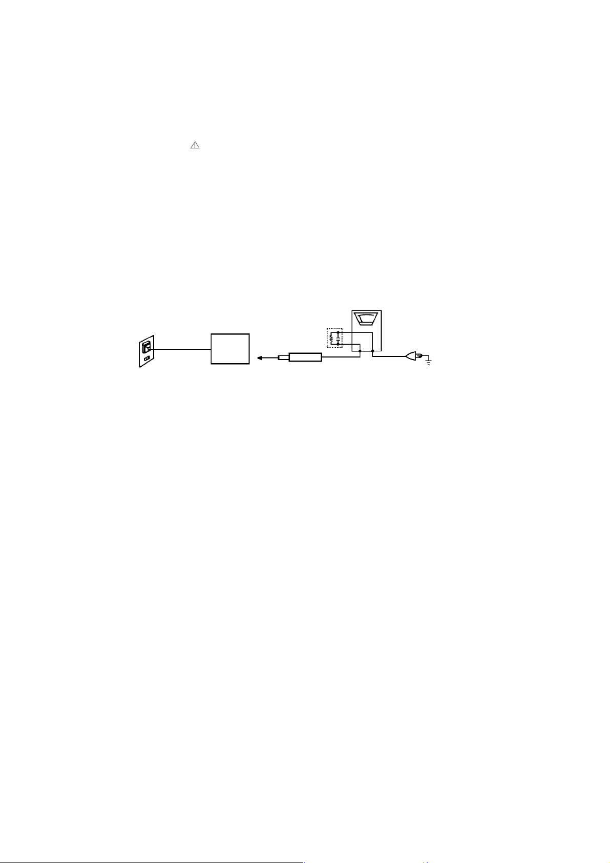
A leakage current check is recommended for this unit. Plug the AC line cord directly into a 120V 60Hz AC
outlet (do not use an isolation transformer for this check). Use a leakage current tester (Fig. 1) or a
metering system which complies with Underwriters Laboratories (UL 1492P). Measure for current from all
exposed metal parts of the cabinet to a known earth ground: particularly, any exposed metal part having a
return path to the chassis. Any current measured must not exceed 0.5mA. Any measurement not within
the limits outlined above are indicative of a potential shock hazard and corrective action must be taken
before returning the unit to the customer.
are critical parts for safety. Replace only with the one described in the parts
(Reading should not be above 0.5mA)
Leakage Current Tester
PRODUCT UNDER TEST
1.5K ohm
0.15 µF
2-Blade polarized
type cord set
Test all exposed
metal surfaces
TEST PROBE
Fig. 1 AC Leakage Test
KNOWN EARTH
GROUND
A1-2
Page 5

IMPORTANT SAFEGUARDS
1.
READ INSTRUCTIONS
All the safety and operating instructions should be read before the unit is operated.
2.
RETAIN INSTRUCTIONS
The safety and operating instructions should be retained for future reference.
3.
HEED WARNINGS
All warnings on the unit and in the operating instructions should be adhered to.
4.
FOLLOW INSTRUCTIONS
All operating and use instructions should be followed.
5.
CLEANING
Unplug this unit from the wall outlet before cleaning. Do not use liquid cleaners or aerosol cleaners. Use a damp
cloth for cleaning.
6.
ATTACHMENTS
Do not use attachments not recommended by the unit’s manufacturer as they may cause hazards.
7.
WATER AND MOISTURE
Do not use this unit near water. For example, near a bathtub, washbowl, kitchen sink, or laundry tub, in a wet
basement, or near a swimming pool.
8.
ACCESSORIES
Do not place this unit on an unstable cart, stand, tripod, bracket, or table. The
unit may fall, causing serious injury, and serious damage to the unit. Use only
with a cart, stand, tripod, bracket, or table recommended by the manufacturer.
8A.
An appliance and cart combination should be moved with care. Quick stops,
excessive force, and uneven surfaces may cause the appliance and cart
combination to overturn.
9.
VENTILATION
Slots and openings in the cabinet and in the back or bottom are provided for ventilation, to ensure reliable
operation of the unit, and to protect it from overheating. These openings must not be blocked or covered. The
openings should never be blocked by placing the unit on a bed, sofa, rug, or other similar surface. This unit
should never be placed near or over a radiator or heat source. This unit should not be placed in a built-in
installation such as a bookcase or rack unless proper ventilation is provided or the manufacturer’s instructions
have been adhered to.
10.
POWER SOURCES
This unit should be operated only from the type of power source indicated on the rating plate. If you are not sure
of the type of power supply to your home, consult your appliance dealer or local power company. For units
intended to operate from battery power, or other sources, refer to the operating instructions.
11.
GROUNDING OR POLARIZATION
This unit is equipped with a polarized alternating-current line plug (a plug having one blade wider than the other).
This plug will fit into the power outlet only one way. This is a safety feature. If you are unable to insert the plug
fully into the outlet, try reversing the plug. If the plug should still fail to fit, contact your electrician to replace your
obsolete outlet. Do not defeat the safety purpose of the polarized plug. If your unit is equipped with a 3-wire
grounding-type plug, a plug having a third (grounding) pin, this plug will only fit into a grounding-type power
outlet. This too, is a safety feature. If you are unable to insert the plug into the outlet, contact your electrician to
replace your obsolete outlet. Do not defeat the safety purpose of the grounding-type plug.
12.
POWER-CORD PROTECTION
Power-supply cords should be routed so that they are not likely to be walked on or pinched by items placed upon
or against them, paying particular attention to cords at plugs, convenience receptacles, and the point where they
exit from the appliance.
13.
LIGHTNING
To protect your unit from a lightning storm, or when it is left unattended and unused for long periods of time,
unplug it from the wall outlet and disconnect the antenna or cable system. This will prevent damage to the unit
due to lightning and power line surges.
14.
POWER LINES
An outside antenna system should not be located in the vicinity of overhead power lines or other electric light or
power circuits, or where it can fall into such power lines or circuits. When installing an outside antenna system,
extreme care should be taken to keep from touching such power lines or circuits, as contact with them might be
fatal.
15.
OVERLOADING
Do not overload wall outlets and extension cords, as this can result in a risk of fire or electric shock.
16.
OBJECT AND LIQUID ENTRY
Do not push objects through any openings in this unit, as they may touch dangerous voltage points or short out
parts that could result in fire or electric shock. Never spill or spray any type of liquid into the unit.
PORTABLE CART WARNING
(symbol provided by RETAC)
S3126A
A1-3
Page 6

IMPORTANT SAFEGUARDS (CONTINUED)
OUTDOOR ANTENNA GROUNDING
17.
If an outside antenna or cable system is connected to the unit, be sure the antenna or cable system is grounded
so as to provide some protection against voltage surges and built-up static charges. Section 810 of the National
Electrical Code, ANSI/NFPA 70, provides information with respect to proper grounding of the mast and supporting
structure, grounding of the lead-in wire to an antenna discharge unit, size of grounding conductors, location of
antenna discharge unit, connection to grounding electrodes, and requirements for the grounding electrode.
SERVICING
18.
Do not attempt to service this unit yourself as opening or removing covers may expose you to dangerous voltage
or other hazards. Refer all servicing to qualified service personnel.
DAMAGE REQUIRING SERVICE
19.
Unplug this unit from the wall outlet and refer servicing to qualified service personnel under the following
conditions:
a.
When the power-supply cord or plug is damaged.
b.
If liquid has been spilled, or objects have fallen into the unit.
c.
If the unit has been exposed to rain or water.
d.
If the unit does not operate normally by following the operating instructions. Adjust only those controls that
are covered by the operating instructions, as an improper adjustment of other controls may result in
damage and will often require extensive work by a qualified technician to restore the unit to its normal
operation.
e.
If the unit has been dropped or the cabinet has been damaged.
f.
When the unit exhibits a distinct change in performance, this indicates a need for service.
REPLACEMENT PARTS
20.
When replacement parts are required, be sure the service technician uses replacement parts specified by the
manufacturer or those that have the same characteristics as the original parts.
Unauthorized substitutions may result in fire, electric shock or other hazards.
SAFETY CHECK
21.
Upon completion of any service or repairs to this unit, ask the service technician to perform safety checks to
determine that the unit is in proper operating condition.
WALL OR CEILING MOUNTING
22.
The product should be mounted to a wall or ceiling only as recommended by the manufacturer.
HEAT
23.
The product should be situated away from heat sources such as radiators, heat registers, stoves, or other
products (including amplifiers) that produce heat.
DISC TRAY
24.
Keep your fingers well clear of the disc tray as it is closing. It may cause serious personal injury.
CONNECTING
25.
When you connect the product to other equipment, turn off the power and unplug all of the equipment from the
wall outlet. Failure to do so may cause an electric shock and serious personal injury. Read the owner's manual of
the other equipment carefully and follow the instructions when making any connections.
SOUND VOLUME
26.
Reduce the volume to the minimum level before you turn on the product. Otherwise, sudden high volume sound
may cause hearing or speaker damage.
SOUND DISTORTION
27.
Do not allow the product output distorted sound for a longtime. It may cause speaker overheating and fire.
HEADPHONES
28.
When you use the headphones, keep the volume at a moderate level. If you use the headphones continuously
with high volume sound, it may cause hearing damage.
LASER BEAM
29.
Do not look into the opening of the disc tray or ventilation opening of the product to see the source of the laser
beam. It may cause sight damage.
DISC
30.
Do not use a cracked, deformed, or repaired disc. These discs are easily broken and may cause serious
personal injury and product malfunction.
NOTE TO CATV SYSTEM INSTALLER
31.
This reminder is provided to call the CATV system installer’s attention to Article 820-40 of the NEC that provides
guidelines for proper grounding and, in particular, specifies that the cable ground shall be connected to the
grounding system of the building, as close to the point of cable entry as practical.
A1-4
Page 7
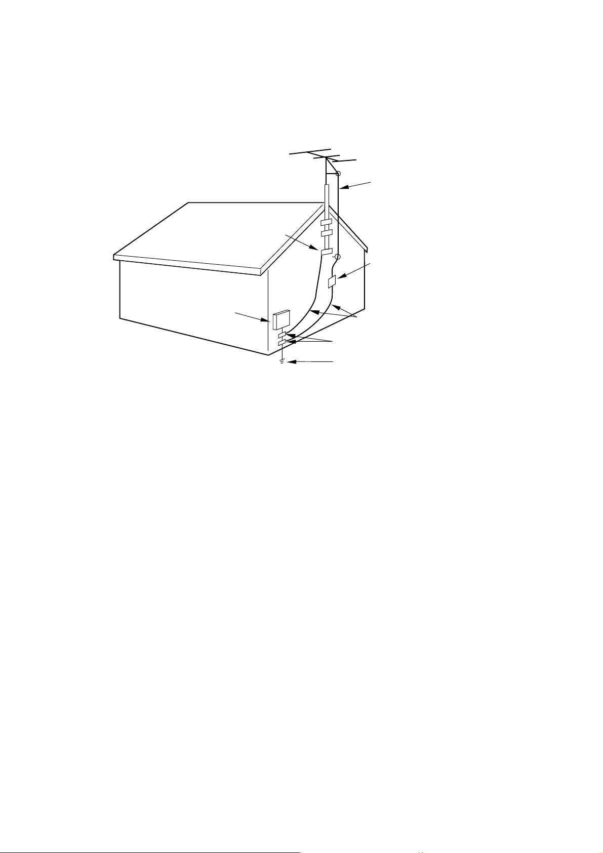
EXAMPLE OF ANTENNA GROUNDING AS PER THE NATIONAL ELECTRICAL CODE
ANTENNA LEAD
IN WIRE
GROUND
CLAMP
ANTENNA
DISCHARGE UNIT
(NEC SECTION 810-20)
ELECTRIC SERVICE
EQUIPMENT
GROUNDING CONDUCTORS
(NEC SECTION 810-21)
GROUND CLAMPS
NEC-NATIONAL ELECTRICAL CODE
S2898A
POWER SERVICE GROUNDING
ELECTRODE SYSTEM
(NEC ART 250, PART H)
A1-5
Page 8
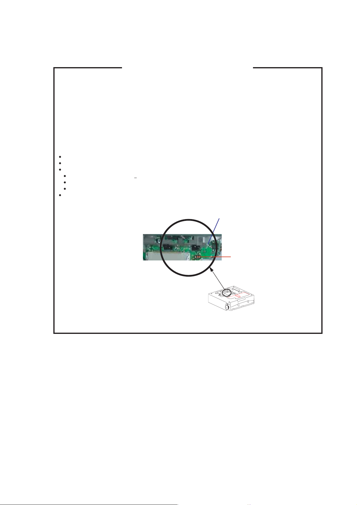
WHEN REPLACING DVD DECK
[ When removing the DVD Deck ]
Before removing Pick Up PCB and DVD PCB connector, the short circuit the position shown in Fig. 1
using a soldering iron. If you remove the DVD Deck with no soldering, the Laser may be damaged.
[ When installing the DVD Deck ]
Remove all the soldering on the short circuit position after the connection of Pick Up PCB and DVD
PCB connector.
NOTE
Before your operation, please read "PREPARATION OF SERVICING" .
Use the Lead Free solder.
Manual soldering conditions
Soldering temperature: 350+5
Soldering time: Within 2 seconds
Soldering combination: Sn-3.0Ag-0.5Cu
When Soldering/Removing of solder, use the draw in equipment over the Pick Up Unit to keep the
Flux smoke away from it.
o
C
Pick Up PCB
Fig. 1
Short circuit using a
soldering iron.
A1-6
Page 9

TABLE OF CONTENTS
CAUTION .....................................................................................................................
IMPORTANT SERVICE SAFETY INFORMATION .....................................................
IMPORTANT SAFEGUARDS .....................................................................................
WHEN REPLACING DVD DECK ................................................................................
TABLE OF CONTENTS ..............................................................................................
GENERAL SPECIFICATIONS ....................................................................................
DISASSEMBLY INSTRUCTIONS
1.REMOVAL OF MECHANICAL PARTS AND P.C. BOARDS ................................
2.REMOVAL AND INSTALLATION OF FLAT PACKAGE IC ..................................
ISP INSTRUCTION .....................................................................................................
RE-WRITE FOR DVD FIRMWARE .............................................................................
WHEN REPLACING EEPROM (MEMORY) IC ...........................................................
ELECTRICAL ADJUSTMENTS ..................................................................................
TROUBLESHOOTING GUIDE ....................................................................................
BLOCK DIAGRAMS
DVD ..........................................................................................................................
SCALER/LVDS/ADC/JACK/AV SWITCH/STEREO SOUND AMP REGULATOR ...
POWER ....................................................................................................................
PRINTED CIRCUIT BOARDS
MAIN ........................................................................................................................
REMOCON/INPUT/OPERATION ............................................................................
HV POWER/POWER ...............................................................................................
DVD DECODER/DVD OUTPUT ..............................................................................
SCHEMATIC DIAGRAMS
SCALER (MAIN) ......................................................................................................
HDMI (MAIN) ...........................................................................................................
INTERFACE/TUNER (MAIN) ...................................................................................
AMP (MAIN) .............................................................................................................
POWER (MAIN) .......................................................................................................
OPERATION/REMOCON ........................................................................................
POWER ....................................................................................................................
HV POWER ..............................................................................................................
DVD OUTPUT ..........................................................................................................
DVD DECODER (DVD DECODER) .........................................................................
SDRAM/FLASH ROM (DVD DECODER0 ................................................................
AV OUT/MUTE/RESERT (DVD DECODER) ...........................................................
INTERCONNECTION DIAGRAM ................................................................................
WAVEFORMS .............................................................................................................
MECHANICAL EXPLODED VIEWS ...........................................................................
MECHANICAL REPLACEMENT PARTS LIST ..........................................................
A1-1
A1-2
A1-3~A1-5
A1-6
A2-1
A3-1~A3-5
B1-1~B1-4
B2-1, B2-2
C1
C-2
C-3
D-1~D-4
E-1~E-9
F-1, F-2
F-3, F-4
F-5, F-6
G-1, G-2
G-3~G-4
G-5, G-6
G-7, G-8
H-1, H-2
H-3, H-4
H-5, H-6
H-7, H-8
H-9, H-10
H-11, H-12
H-13, H-14
H-15, H-16
H-17, H-18
H-19, H-20
H-21, H-22
H-23, H-24
H-25, H-26
I-1~I-3
J1-1~J1-2
K1-1~K1-3
A2-1
Page 10
GENERAL SPECIFICATIONS
G-1 TV LCD LCD Size / Visual Size 20.04 inch / 508.9mmV
G-2 DVD System Color System NTSC
G-3 Tuning Broadcasting System US System M
G-4 Signal Video Signal Input Level 1 V p-p/75 ohm
G-5 Power Power Source AC 110V~240V, 50/60Hz
G-6 Regulation Safety UL/CSA
G-7 Temperature Operation +5
G-8 Operating Humidity Less than 80% RH
System LCD Type Color TFT LCD
Color System NTSC
Speaker 2 Speaker
Sound Output Max 3W + 3W
Disc DVD, CD-DA, CD-R/RW, Video CD
Disc Diameter 120 mm
Drive SL265WR
Search speed Fwd 4 step
Slow speed Fwd 1/7 -1/2 times
System Tuner and System 1Tuner
Receive CH Destination US (W/CABLE)
Intermediate Picture(FP) 45.75MHz
Frequency Sound(FS) 41.25MHz
Preset CH No
Stereo/Dual TV Sound US-Stereo
Tuner Sound Muting Yes
RGB Signal Output Level -Audio Signal Input Level -8.0dBm/50k ohm
Power Consumption at AC 100W at 110V~240V 50/60Hz
Protector Power Fuse Yes
Number of Pixels 1366(H) x 768(V)
View Range Left/Right 80/80 degree
Position Front
Size 1.8 x 3.9 inch
Impedance 8 ohm
10%(Typical) ---
Rev 4 step
Rev 1/7 -1/2 times
CH Coverage 2~69, 4A, A-5~A-1, A~I, J~W, W+1~W+84
FP-FS 4.50MHz
Output Level -S/N Ratio (Weighted) -Horizontal Resolution at DVD Mode --
Output Level at DVD --
Digital Output Level 0.5 V p-p/75 ohm
S/N Ratio at DVD (Weighted) -Harmonic Distortion -Frequency Response : at DVD --
DC --
Stand by (at AC) 3W at 110V~240V 50/60Hz
Energy Star Yes
Per Year -- kWh/Year
Safety Circuit Yes
IC Protector(Micro Fuse) Yes
Radiation FCC/IC
Laser DHHS
Storage -20
Up/Down 80/60 degree
DVD-R/RW (Video Format Only)
Actual 2-45 times (DVD, VIDEO CD)
Actual 2-45 times (DVD, VIDEO CD)
Actual --
Actual --
at TV --
at Video CD --
at SVCD --
at CD --
at DC --
4-40 times (CD)
4-40 times (CD)
--
o
C ~ +35oC
o
C ~ +60oC
A3-1
Page 11
GENERAL SPECIFICATIONS
G-9 Clock and Clock Yes
G-10 Remote Unit RC-LT
Timer Sleep Timer Max Time 120 Min
On Timer Program
Off Timer Program No
Game Timer
Wake Up Timer No
Timer Back-up (at Power Off Mode) more than -- Min Sec
Control Glow in Dark Remocon Yes
Remocon Format TOSHIBA
Format TOSHIBA
Custom Code 40-BF h ,44-BB h ,45-BA h ,45-BC h
Power Source Voltage(D.C) 3V
Total Keys 49 Keys
Keys
Step
UM size x pcs UM-4 x 2 pcs
Power
EJECT
SLEEP
TV/DVD
1
2
3
4
5
6
7
8
9
0
100 / JUMP
DISPLAY
SUBTITLE
AUDIO SELECT
INPUT / ZOOM
MUTE
CH +
CH VOL +
VOL PLAY MODE
DVD MENU
UP
LEFT / FAV ENTER
RIGHT / FAV +
DOWN
TV MENU/SETUP
EXIT / CANCEL
GAME
PIC SIZE
PAUSE
PLAY
STOP
CH RTN /<SKIP
SEARCH SEARCH +
Closed Caption / SKIP>
< SLOW
ANGLE
Marker
SLOW >
TOP MENU
RETURN
REPEAT A-B
10 Min
Yes
Yes
Yes
Yes
Yes
Yes
Yes
Yes
Yes
Yes
Yes
Yes
Yes
Yes
Yes
Yes
Yes
Yes
Yes
Yes
Yes
Yes
Yes
Yes
Yes
Yes
Yes
Yes
Yes
Yes
Yes
Yes
Yes
Yes
Yes
Yes
Yes
Yes
Yes
Yes
Yes
Yes
Yes
Yes
Yes
Yes
Yes
Yes
Yes
Yes
Yes
A3-2
Page 12
GENERAL SPECIFICATIONS
(
)
G-11 Features Auto Shut Off Yes
(TV) Auto Search Yes
Power On Memory Yes
Comb Filter Yes
Game Position Yes
Auto Setup(Language/CH Program) Yes
Picture Setting(TV) Yes
Picture Setting(PC) Yes
Audio MTS Yes
Tuning CH Program Yes
Label CH Label Yes
Favorite CH Yes
V-Chip Yes
RRT Setup
Lock Hotel Lock No
OSD Language
Closed Caption
CC Advanced
Picture Size Yes
Picture Scroll No
Cinema Mode Yes
Aspect Yes
Backlight Yes
PFC(Power Factor circuit)
Freeze frame No
PIP/POP No
Direct Input Selection Yes
PC Monitor Input Yes
HDMI Input Yes
Component Input Yes
Mode(Picture Preference) Yes
Brightness , Contrast , Color Yes
Tint
Sharpness Yes
Color Temperature Yes
Cable Clear Yes
BRIGHTNESS , CONTRAST Yes
HOR POSITION , VER POSITION Yes
PHASE , CLOCK Yes
AUTO ADJUST No
RED , GREEN , BLUE Yes
Tone Control (Bass/Treble/Balance) Yes
Stable Sound Yes
Surround No
BBE No
SRS WOW (SRS 3D/Focus/Tru Bass) No
Variable Audio Out No
TV/Cable Yes
ADD/DELETE Yes
Video Label Yes
Type
Channel Lock Yes
Video Lock Yes
Panel Lock Yes
VGA (640x480) Yes (60Hz)
VGA (720x400) Yes (70Hz)
WVGA (848x480) Yes (60Hz)
SVGA (800x600) Yes (60Hz)
XGA (1024x768) Yes (60Hz)
WXGA (1280x768) Yes (60Hz)
WXGA (1280x720) Yes (60Hz)
WXGA (1360x768) Yes (60Hz)
SXGA (1280x1024) No
VGA (640x480) Yes (60Hz)
720x480i (4:3) Yes (60Hz)
720x480i (16:9) Yes (60Hz)
720x480p (4:3) Yes (60Hz)
720x480p (16:9) Yes (60Hz)
720x576i (4:3) No
720x576i (16:9) No
720x576p (4:3) No
720x576p (16:9) No
1280x720p Yes (60Hz)
1920x1080i Yes (60Hz)
720x480i (4:3) Yes (60Hz)
720x480i (16:9) Yes (60Hz)
720x480p (4:3) Yes (60Hz)
720x480p (16:9) Yes (60Hz)
720x576i (4:3) No
720x576i (16:9) No
720x576p (4:3) No
720x576p (16:9) No
1280x720p Yes (60Hz)
1920x1080i Yes
3 -D
Yes
USA Type
English French Spanish
Yes
A3-3
No
No
No
60Hz
Page 13
GENERAL SPECIFICATIONS
Features Tray Lock Yes
(DVD) Video CD Playback Yes
G-12 Accessories Owner's Manual Language English / French
SVCD Playback
Overlay Graphics And Text No
Command List No
Entry Point Jump No
MP3 Playback Yes
Divx Playback Yes
DMF Support No
JPEG Yes
WMA Yes
Digital Out (Dolby Digital) Yes
(MPEG) Yes
(PCM) Yes
(DTS) Yes
Down Mix Out (Dolby Digital) Yes
(DTS) No
Closed Caption Yes
Screen Saver No
Audio DAC 192kHz / 24bit
w/Guarantee Card Yes
Remote Control Unit Yes
Rod Antenna
Poles --
Terminal -Loop Antenna
Terminal -U/V Mixer
DC Car Cord (Center+)
Guarantee Card
Warning Sheet
Circuit Diagram
Antenna Change Plug
Service Facility List
Important Safeguard
Dew/AHC Caution Sheet
Quick Set-up Sheet
Battery Yes
UM size x pcs UM-4 x 2 pcs
OEM Brand No
AC Adapter
AC Cord (for AC Adapter)
AV Cord (2Pin-1Pin)
Registration Card (NDL Card) Yes
300ohm to 75ohm Antenna Adapter
Sheet Information (Return) Yes(USA,CND version)
Sheet Information (HDMI) No
Screw for wall hanging No
No
No
No
No
No
No
No
No
No
No
No
No
No
No
No
No
No
A3-4
Page 14
GENERAL SPECIFICATIONS
G-13 Interface Switch Top Power (Tact) Yes
Indicator Power / Stand-by Yes(GREEN / RED)
Terminals Rear Video Input 1 RCA x 1
Side Video Input 2 No
G-14 Set Size Approx. W x D x H (mm) 554 x 233 x 448
G-15 Weight Net (Approx.) 10.7kg (23.5 lbs)
G-16 Carton Master Carton No
Gift Box Material Double/ Full Color
Drop Test 2 Corner / 2 Edges / 2 Surfaces
Container Stuffing (40' container) 492
G-17 Material Cabinet Front PS 94V0 DECABROM
PCB Non-Halogen Demand No
G-18 Environment Environmental standard requirement (by buyer) Green PROCUREMENT of TOSHIBA
Pb-Free Phase 3 (Phase 3A)
Channel Up/Menu Up Yes
Channel Down/Menu Down Yes
Volume Up/Menu > Yes
Volume Down/Menu < Yes
Menu Yes
Play Yes
Eject Yes
Skip+, Search+ Yes
Skip-, Search- Yes
Still/Pause No
Stop Yes
Main Power SW No
Input Select Yes
Power No
Stand-by No
On Timer No
Audio Input 1
S - Input 1
Video Input 2 RCA x 1
Audio Input 2
S- Input 2 No
Video Output No
Audio Output No
Component Input
Analog Audio RCA x 2(L/MONO, R)
HDMI Input
Analog Audio PC Monitor Audio Input Alternative
PC Monitor Input
Analog Audio RCA x 2(L/MONO, R)
Digital Audio Output Optical (DVD Only)
DC Jack No
VHF/UHF Antenna Input
Other Terminal
AC Outlet No
Audio Input 2 No
PC Monitor Input(w/ Analog Audio L/R) No
Other Terminal No
w/o Handle, Stand Approx. W x D x H (mm)
Net w/o Handle, Stand (Approx.) 9.4kg (20.8 lbs)
Gross (Approx.) 13.5kg (29.8 lbs)
Content --- Sets
Material --- / ---
Dimensions W x D x H(mm) ---
Description of Origin ---
W/Color Photo Label No
W/Handle No
Dimensions W x D x H(mm) 654 x 338 x 565
Description of Origin No(Assembled In Thailand)
Height (cm) 65
Rear PS 94V0 DECABROM
Eyelet Demand Yes
Measures for Whisker Yes
RCA x 2(L/MONO, R)
Yes
RCA x 2(L/MONO, R)
RCA x 3
HDMI x 1
Dsub15pin x 1
F Type
Headphone
554 x 105 x 402
Sets
A3-5
Page 15
DISASSEMBLY INSTRUCTIONS
1. REMOVAL OF MECHANICAL PARTS
AND P.C. BOARDS
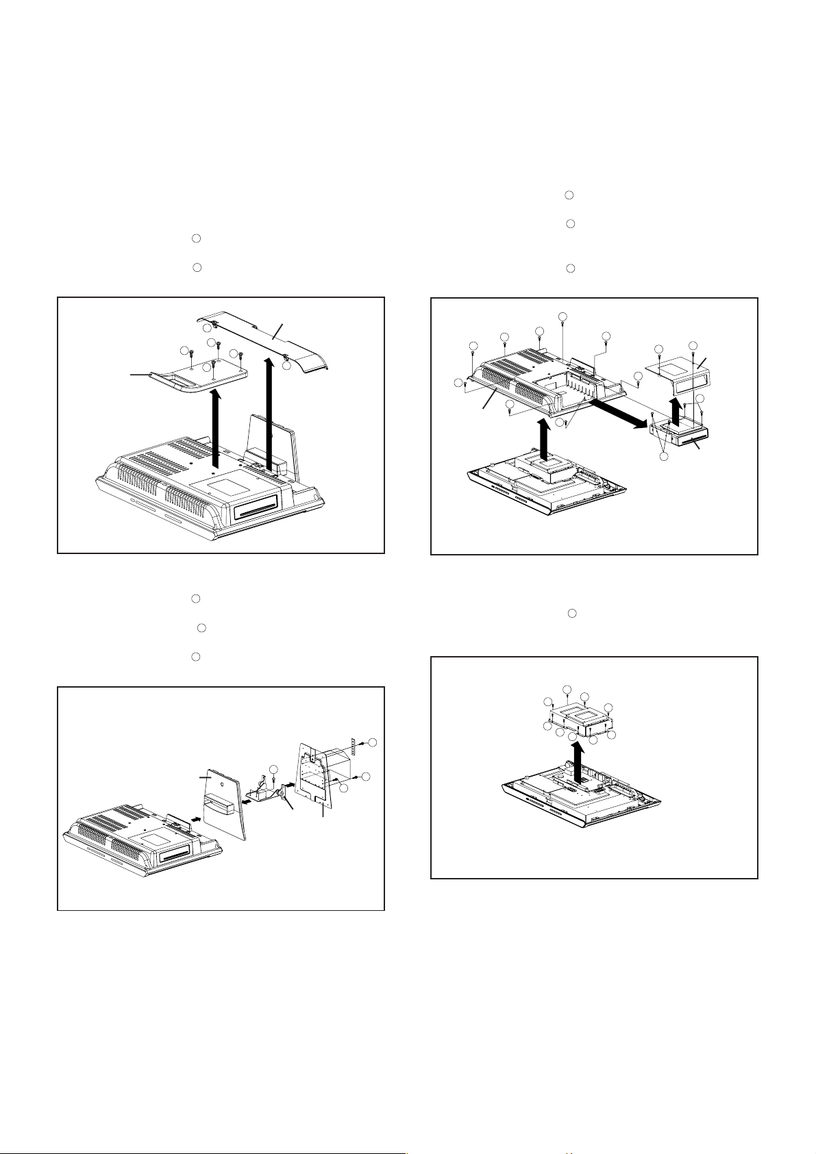
1-1: HANDLE/BACK COVER (Refer to Fig. 1-1)
1.
Remove the 4 screws .
2.
Remove the Handle in the direction of arrow (A).
3.
Unlock the 2 supports .
4.
Remove the Back Cover in the direction of arrow (B).
Handle
1
2
2
1
1
1
(A)
Back Cover
1
2
(B)
Fig. 1-1
1-3: BACK CABINET (Refer to Fig. 1-3)
1.
Remove the 2 screws .
2.
Remove the DVD Shield in the direction of arrow (A).
3.
Remove the 4 screws .
1
2
4. Disconnect the following connector: (AH301813)
5. Remove the TD-20DVD(mtk) Ass’y in the direction of arrow (B).
6.7.Remove the 9 screws .
3
Remove the Back panel in the direction of arrow (C).
3
3
3
Back Panel
3
3
3
3
(C)
3
3
(B)
1
1
(A)
DVD Shield
2
TD-20DVD(mtk) Ass’y
2
Fig. 1-3
1-2: HINGE ASS'Y (Refer to Fig. 1-2)
Stand
1
2
3
1
(C)
(A)
(B)
Hinge Ass'y
Angle Stand
1.
Remove the 5 screws .
2.
Remove the Stand in the direction of arrow (A).
3.
Remove the 13 screws .
4.
Remove the Angle Stand in the direction of arrow (B).
5.
Remove the 4 screws .
6.
Remove the Hinge Ass'y in the direction of arrow (C).
2
3
Fig. 1-2
1-4: HANDLE BRACKET AND MAIN PCB SHIELD
(Refer to Fig. 1-4)
1.2.Remove the 9 screws .
1
Remove the Handle Bracket and Main PCB Shield in the
direction of arrow.
1
1
1
1
2
1
1
1
1
1
Fig. 1-4
B1-1
Page 16
DISASSEMBLY INSTRUCTIONS
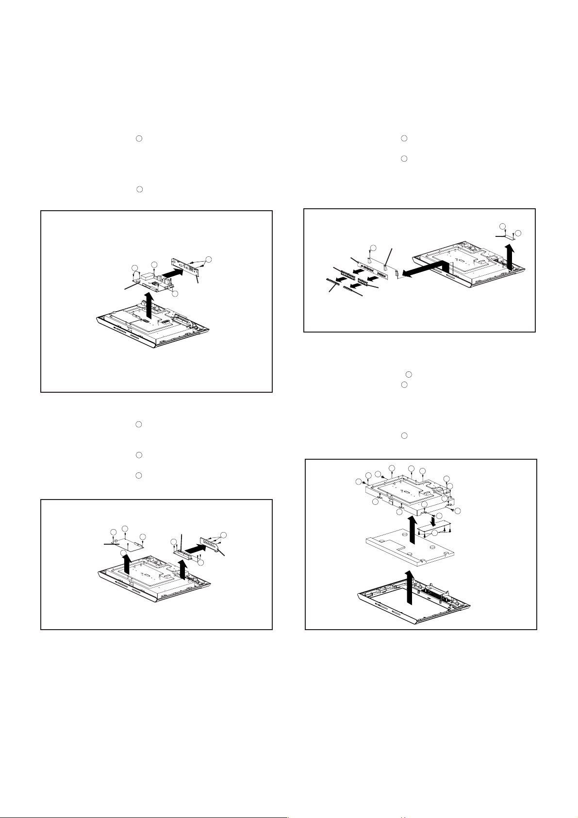
1-5: MAIN PCB (Refer to Fig. 1-5)
1.
Remove the 2 screws .
2.
Remove the Back Plate B in the direction of arrow (A).
3.
Disconnect the following connectors:
1
(AH301810, AH301814, AH301815, AH301816,
AH301818, AH301819).
4.
Remove the 5 screws .
2
5. Remove the Main PCB in the direction of arrow (B).
1
Back Plate B
Main PCB
2
2
(A)
2
(B)
1-6: POWER PCB / INPUT PCB (Refer to Fig. 1-6)
1.2.Remove the 4 screws .
1
Disconnect the following connector: (AH301817)
3.
Remove the Power PCB in the direction of arrow (A).
4.
Remove the 3 screws .
5.
Remove the Back Plate A in the direction of arrow (B).
6.
Remove the 4 screws .
7.
Remove the Input PCB in the direction of arrow (C).
Power PCB
2
3
1
1
1
(A)
Input PCB
1
3
(B)
(C)
3
2
Back Plate A
Fig. 1-5
1-7: REMOCON PCB / OPERATION PCB (Refer to Fig. 1-7)
1.
Remove the 2 screws .
2.
Remove the Remocon PCB in the direction of arrow (A).
3.
Remove the 3 screws .
1
2
4. Remove the Operation PCB Fixity in the direction of arrow (B).
5.6.Remove the Operation PCB in the direction of arrow (C).
Remove the Function Button in the direction of arrow (D).
1
1
(A)
Operation PCB
Button Frame A
Function Button
(D)
Operation PCB Fixity
2
(C)
(C)
Button Frame B
(D)
Function Button
Remocon PCB
(B)
Fig. 1-7
1-8: LCD COVER / LCD PANEL / HV POWER
(Refer to Fig. 1-8)
1.
Remove the 10 screws .
2.
Remove the 4 screws .
3.
Remove the LCD Cover in the direction of arrow (A).
4.
Disconnect the connector between LCD panel and
1
2
HV power PCB.
5.
Remove the LCD Panel in the direction of arrow (B).
6.
Remove the 4 screws .
7.
Remove the HV Power PCB in the direction of arrow (C).
1
2
1
3
1
1
(B)
1
1
1
1
1
1
(C)
(A)
2
2
3
2
Fig. 1-6
Fig. 1-8
B1-2
Page 17
DISASSEMBLY INSTRUCTIONS
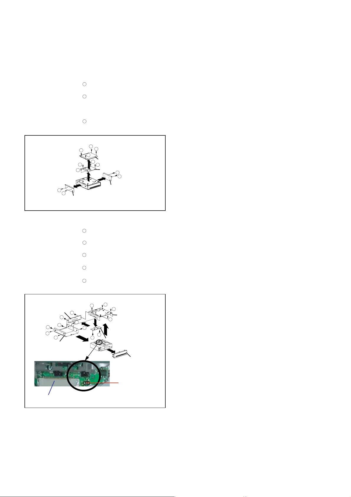
1-9: DECODER PCB (Refer to Fig. 1-9)
2
3
3
(C)
(A)
DVD Bracket
1
2
3
2
2
(B)
1
2
3
4
5
2
Decoder PCB cover
3
3
Decoder PCB
(A)
DVD Bracket
1
1
Fig. 1-9
1.
Remove the 4 screws .
2.
Remove the DVD Bracket in the direction of arrow (A).
3.
Remove the 4 screws .
4.
Remove the Decoder PCB Cover in the direction of arrow (B).
5.
Disconnect the following connectors:
(AH301898, AH301899, AH301900, AH301901).
6.
Remove the 4 screws .
7.
Remove the Decoder PCB in the direction of arrow (C).
1
1
1-10: OUTPUT PCB / DVD MECHA (Refer to Fig. 1-10)
1.2.Remove the 4 screws .
Remove the DVD Front panel in the direction of arrow (A).
3.
Remove the 2 screws .
4.
Remove the DVD Mecha in the direction of arrow (B).
5.
Remove the 2 screws .
6.
Remove the DVD Back Panel in the direction of arrow (C).
7.
Remove the 2 screws .
8.
Remove the Output PCB in the direction of arrow (D).
9.
Remove the 4 screws .
10.
Remove the DVD Top Panel in the direction of arrow (E).
DVD Back Panel
2
1
1
Bottom Panel
Pick Up PCB
5
5
3
3
1
2
(C)
(B)
1
4
(D)
4
5
DVD Top Panel
5
(E)
Output PCB
(A)
DVD Front panel
Short circuit using a
soldering iron.
Fig. 1-10
B1-3
Page 18
DISASSEMBLY INSTRUCTIONS
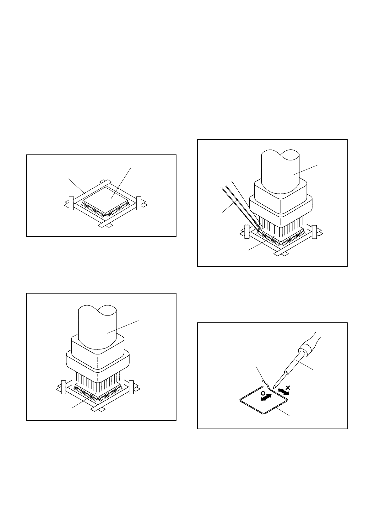
2. REMOVAL AND INSTALLATION OF FLAT
PACKAGE IC
REMOVAL
1. Put the Masking Tape (cotton tape) around the Flat
Package IC to protect other parts from any damage.
(Refer to Fig. 2-1.)
NOTE
Masking is carried out on all the parts located within
10 mm distance from IC leads.
Masking Tape
(Cotton Tape)
2. Heat the IC leads using a blower type IC desoldering
machine. (Refer to Fig. 2-2.)
NOTE
Do not add the rotating and the back and forth directions force on the IC, until IC can move back and forth
easily after desoldering the IC leads completely.
IC
Fig. 2-1
Blower type IC
desoldering machine
3. When IC starts moving back and forth easily after
desoldering completely, pickup the corner of the IC using
a tweezers and remove the IC by moving with the IC
desoldering machine. (Refer to Fig. 2-3.)
NOTE
Some ICs on the PCB are affixed with glue, so be
careful not to break or damage the foil of each IC
leads or solder lands under the IC when removing it.
Blower type IC
desoldering machine
Tweezers
IC
4.5.Peel off the Masking Tape.
Absorb the solder left on the pattern using the Braided
Shield Wire. (Refer to Fig. 2-4.)
NOTE
Do not move the Braided Shield Wire in the vertical
direction towards the IC pattern.
Fig. 2-3
Braided Shield Wire
Soldering Iron
IC
Fig. 2-2
IC pattern
Fig. 2-4
B2-1
Page 19
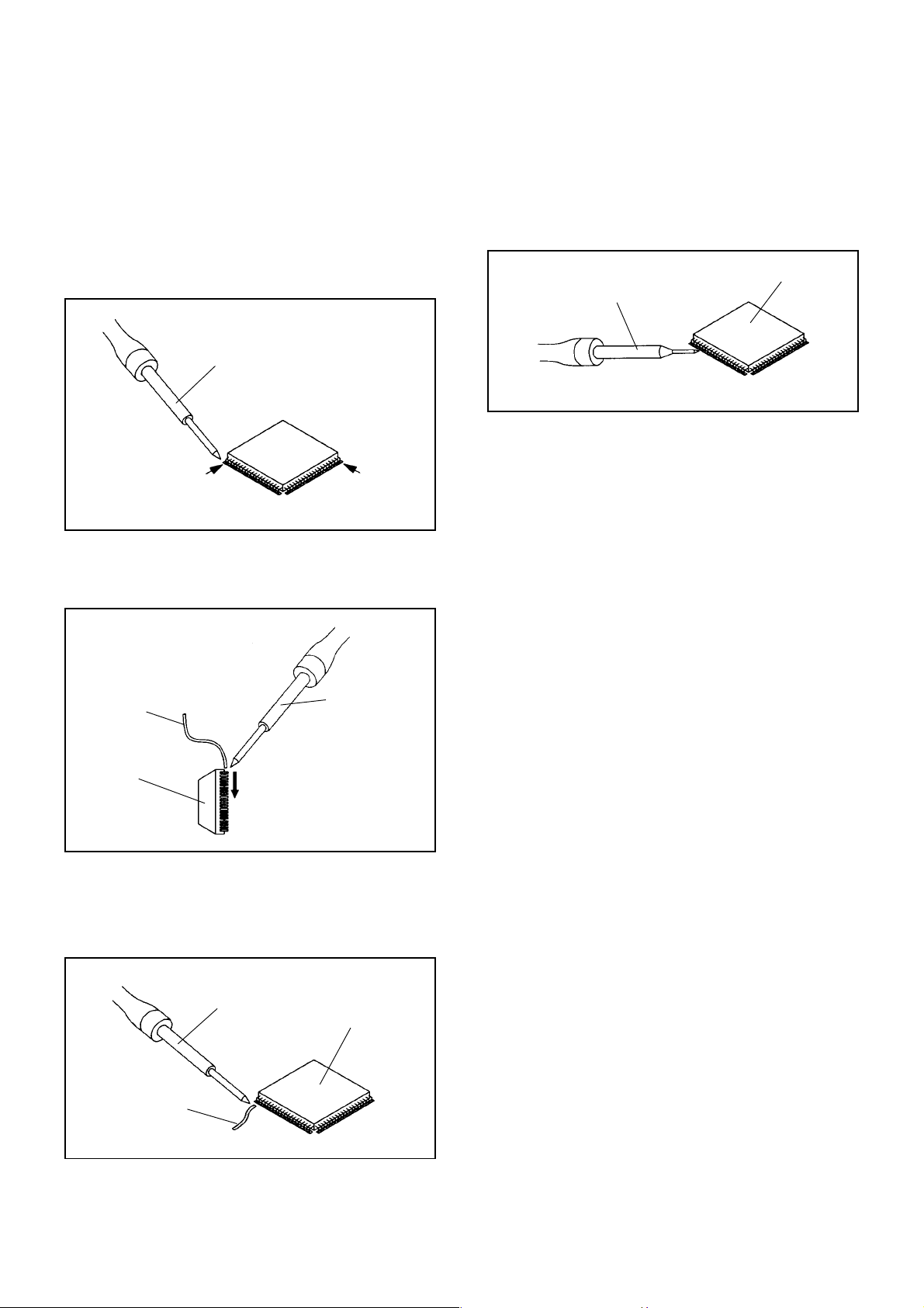
DISASSEMBLY INSTRUCTIONS
INSTALLATION
1. Take care of the polarity of new IC and then install the
new IC fitting on the printed circuit pattern. Then solder
each lead on the diagonal positions of IC temporarily.
(Refer to Fig. 2-5.)
Soldering Iron
Solder temporarily
Solder temporarily
Fig. 2-5
2. Supply the solder from the upper position of IC leads
sliding to the lower position of the IC leads.
(Refer to Fig. 2-6.)
4. When bridge-soldering between terminals and/or the
soldering amount are not enough, resolder using a Thintip Soldering Iron. (Refer to Fig. 2-8.)
IC
Thin-tip Soldering Iron
Fig. 2-8
5. Finally, confirm the soldering status on four sides of the
IC using a magnifying glass.
Confirm that no abnormality is found on the soldering
position and installation position of the parts around the
IC. If some abnormality is found, correct by resoldering.
NOTE
When the IC leads are bent during soldering and/or
repairing, do not repair the bending of leads. If the
bending of leads are repaired, the pattern may be
damaged. So, be always sure to replace the IC in this
case.
Solder
IC
Supply soldering
from upper position
to lower position
Soldering Iron
Fig. 2-6
3. Absorb the solder left on the lead using the Braided
Shield Wire. (Refer to Fig. 2-7.)
NOTE
Do not absorb the solder to excess.
Soldering Iron
IC
Braided Shield Wire
Fig. 2-7
B2-2
Page 20

ISP INSTRUCTION
1. Connect one end of the Jig to the LPT jack of the computer, and the other
end to the VGA connector PC at the side of the TV.
2. Press " up + down + left + right + menu + enter " on the remote control in
order to open the factory menu of 20HLV. Select [ES] on pressing arrow
button, then press "enter" on the remote control.
3. Turn TV power off once and turn it on again.
4. Run "ISP_Tool V3.6.exe"(Refer to Fig. 1)
9. Unselect "Program" and "Verify", click "Run" (Refer to Fig. 6).
5. Choose the “ CONFIG” , click “Auto detech” , the “status” will be “OK”.
Fig. 1
(Refer to Fig. 2)
Fig. 2
6. Click "connect", if it clue to "Device Type is PM25LV040" mean connector
of upgrade fixture OK, if it clue to "Can't Entry ISP Mode!!", please secure
connection of Jig firmly, then click "connect", if it clue to " Device Type is
PM25LV040". (Refer to Fig. 3)
Fig. 3
7. Click "Read" to enter next inter face, Click "Read" to select upgrade file
(*.bin). (Refer to Fig. 4)
10. If it clue to "Blank OK", unselect "Blank" and select "Program" and
Fig. 6
"Verify", click "Run" to enter upgrade status (Refer to Fig. 7).
Fig. 7
11. If it clue to "Program OK" and "Verify OK", it mean upgrade succeed
(Refer to Fig. 8).
Fig. 8
12. If it clue to "Program Error" (Refer to Fig. 9), click "Run" to repeat
currently setp,title it clue to "Program OK" and "Verify OK"
(Re fer t o Fig. 8) .
8. Sure upgrade file read, Click "Auto" to enter next interface
Fig. 4
(Refer to Fig. 5).
Fig. 5
Fig. 9
13. Click "DIS CON" to exit ISP upgrade program (Refer to Fig. 10).
Fig. 10
C-1
Page 21

RE-WRITE FOR DVD FIRMWARE
1.
Turn on the power, and set the DVD mode.
2.
Confirm that the "OPEN" will be appeared on the screen.
3.
Insert the Up-Date Disc. Automatic read will start and "Upgrade file detected, Upgrade? Press PLAY key to start"
will be displayed on the screen.
4.
Press PLAY button on the remocon to start upgrade.
NOTE: Do not turn off the unit on the way or operate the keys on the unit and remocon.
Up-Date error will happen and can not be done with the Up-Date of Up-Date Disc.
After the Up-Date, Logo screen will appear.
5.
Unplug the AC cord, then plug it in.
8.
CHECK FOR THE FIRMWARE VERSION
Turn on the power, and set the DVD mode.
9.
Press "SETUP" "RETURN" "1" "2" "3" button on the remote control. Firmware version will be displayed on the
10.
top bottom of the screen.
060704 19:26 SASn 5 1.0
Turn off the power
11.
060704 19:26 SASn 5 1.0
Fixed
Release date (Example: 2006.7.4, 19:26)
When the changed version displays, the Re-write will be completed.
Released No.
C-2
Page 22

WHEN REPLACING EEPROM (MEMORY) IC
CONFIRMATION OF INITIAL DATA
Turn POWER on.
1.
Press "up+ down + left + right + menu + enter" on the remote control in turn to enter Factory mode as FIG 1.
2.
FACTORY MENU
SOURCE
ADC ADJ
COLOR TEMP
EEPROM ADDR .
VERSION :
07 / 03 / 06
16 : 57 : 31
Using the UP/DOWN/LEFT/RIGHT button on the remote, step through the ADDRESS until required ADDRESS
3.
DATA
SAVE
OFFES
value "FFF" has been selected as FIG 2.
FACTORY MENU
SOURCE
ADC ADJ
COLOR TEMP
EEPROM ADDR .
VERSION :
07 / 03 / 06
16 : 57 : 31
DATA
SAVE
OFFES
ANTE01tream HD
000
FF
FIG. 1
ANTE01tream HD
FFF
FF
FIG. 2
When satisfied correct DATA has been entered, press "right" to save the change, then press "enter" to finish ADDRESS
4.
input.
Unplug the AC cord, then plug it in.
5.
Turn POWER on.
6.
The STARTING SETUP feature appears. Setup your TV/DVD by the owner manual.
7.
C-3
Page 23

ELECTRICAL ADJUSTMENTS
1. ADJUSTMENT PROCEDURE
Press "up+ down + left + right + menu + enter" on the remote control in turn to enter Factory mode as FIG 1-1.
FACTORY MENU
SOURCE
ADC ADJ
COLOR TEMP
EEPROM ADDR .
DATA
SAVE
OFFES
VERSION :
07 / 03 / 06
16 : 57 : 31
Fig. 1-1
Press "left" or "right" to select "ANTE01", "VIDEO01", "VIDEO02", "GAME02", "COLORS", "HDMI", "PC" items,
Press "up" or "down" to select each items, and Press "left" or "right" to enter each items. Example: FIG 1-2.
ANTE01tream HD
000
FF
SOURCE
COLOR TEMP
R
G
B
ANTE01tream HD
COOL
122
118
133
Fig. 1-2
Press "left" or "right" to select "COOL", "NORMAL", "WARM" items, Press "up" or "down" to adjustment each items.
Press "EXIT" on the remote control to exit Factory mode
Confirmation of Fixed Value (Step No.)
Please check if the fixed values of each of the adjustment items are set correctly referring below.
(ANTE01/VIDEO01/VIDEO02/GAME02/COLORS/HDMI/PC)
FUNCTION
COOL
MEDI
WARM
ANTE01 VIDEO01 VIDEO02 GAME02 COLORS HDMI PC
Step No.
122 122 122 122 122 122 128
R
118 118 118 118 118 118 128
G
133 133 133 133 133 133 128
B
124 124 124 124 124 124 136
R
120 120 120 120 120 120 128
G
130 130 130 130 130 130 128
B
126 126 126 126 126 126 128
R
122 122 122 122 122 122 128
G
128 128 128 128 128 128 136
B
D-1
Page 24

ELECTRICAL ADJUSTMENTS
2. WHITE BALANCE ADJUSTMENT
Press "up+ down + left + right + menu + enter" on the remote control in turn to enter Factory mode as FIG 2-1.
FACTORY MENU
SOURCE
ADC ADJ
COLOR TEMP
EEPROM ADDR .
DATA
SAVE
OFFES
VERSION :
07 / 03 / 06
16 : 57 : 31
Fig. 2-1
Press "left" or "right" to select "COLORS", "PC" items,
Press "up" or "down" to select "ADC ADJ" items, and Press "left" or "right" to enter this items. Example: FIG 2-2.
COLORStream HD
000
FF
SOURCE
R off.
G off.
B off.
R Gain
G Gain
B Gain
AUTOTONE
COLORStream HD
127
138
127
63
51
61
Fig. 2-2
Press "up" or "down" to select "AUTOTONE" items, Press "right" to "ADC ADJ" automatic adjustment.
Press "enter" on the remote control to finish the "ADC ADJ" automatic adjustment.
Press "EXIT" on the remote control to exit Factory mode.
D-2
Page 25

D-4
JP1
CZ1
POWER PCB
CZ3
AH301815
CZ4
AH301810
CPU UPDATE
AH301816
HDCP
XP12
XP10
XP6
XP5
XP2
XP7
XP3
UN2
XP4
MIAN PCB
JN4
JN6
JN2
JN7
JN5
JN1
XP8
1
OPERATION PCB
AH301817
ELECTRICAL ADJUSTMENTS
CN1
CN7
CN6
CN5
HV POWER PCB
CN3
CN2
CN4
LCD PANEL
XS3
AH301898
XS1
XS2
AH301813
VD9
XS002
1
XS1
1
AH301900
XS8
AH301819
OUTPUT PCB
DECODER PCB
1
AH301818
SPEAKER
U3
JP1
REMOCON PANEL
U4
AH301814
1
U2
INPUT PCB
U1 U7 U8 U9 U10 U11
3. ELECTRICAL ADJUSTMENT PARTS LOCATION GUIDE (WIRING CONNECTION)
AH301901
AH301899
DVD MECHA
D-3
Page 26

No work / LED is off
TROUBLESHOOTING GUIDE
Check if power
connection isnormal
Yes
Check if voltage of
Power PCB CZ3,
CZ4 is normal
Yes
Check if fuse F1 is normal
Yes
Check if voltage of XP3
pin2 is normal
Yes
No
No
No
No
Replace power connection
Replace Power PCB
Replace fuse and eliminate short
or open situation
Replace Main PCB
Replace RMC PCB
E-1
Page 27

No work / LED is red
TROUBLESHOOTING GUIDE
Check if RMC
PCB is normal
Yes
Check if voltage of
N9,N4,U8 is normal
Yes
Replace Main PCB
No
Replace RMC PCB
No
Replace N9 or N4 or U8
E-2
Page 28

No Picture / LED is blue
TROUBLESHOOTING GUIDE
Check if backlight is normal
Yes
Check if connector
of XP6 is normal
Yes
Check if signal of
LVDS is normal
Yes
Replace LCD panel
No No
Check if voltage of HV
power PCB U1,U2 is normal
Yes
Replace HV power PCB
No
Replace XP6
No
Replace Main PCB
Check the power and
control signal of XP5
in main PCB is normal
Yes
No
Replace Main PCB
No TV Picture
Check if voltage
of N3 pin1 is 5V
Yes
Replace UN2 HF
No
Replace Main PCB
E-3
Page 29

No CVBS/SVIDEO Picture
TROUBLESHOOTING GUIDE
Check if SVIDEO/CVBS
signal of U3 is normal
Yes
Check if SVIDEO/CVBS
signal of U9 pin54,53
is normal
Yes
Replace Main PCB
No HDMI
Check if signal of
JN2 is normal
Yes
No
Replace Input PCB
No
Replace connec wire
No
Replace connection
Check if voltage of
U35,U14 pin8 is normal
Yes
Check if signal of
U9 pin 14,15 is normal
Yes
Replace Main PCB
No
Replace U35 or U14
No
Replace U9
E-4
Page 30
No DVD picture
TROUBLESHOOTING GUIDE
Check if voltage of
XP7 pin 15 is normal
Yes
Check if signal of
XP7 pin 6,7,8 is normal
Yes
Replace Main PCB
No
Replace Main PCB
No
Replace DVD ass'y
E-5
Page 31

No VGA picture
TROUBLESHOOTING GUIDE
Check if signal of JN4
pin 1,2,3,12,13,15 is normal
Yes
Check if volatge of
U16 pin 8 is normal
Yes
Check if signal of
U9 pin 16~28 is normal
Yes
Check if volatge of
U16 pin 8 is normal
Yes
No
Replace connection
No
Replace N9
No
Replace Main PCB
No
Replace N9
Check if signal of
LVDS is normal
Yes
Replace Main PCB
No
Replace U9
E-6
Page 32

No AV1/AV2 audio
TROUBLESHOOTING GUIDE
Check if signal of XP8
pin 5,7,11,13 is normal
Yes
Check if signal of
U9 pin 85,86 is normal
Yes
Check if signal of
U2 pin 1,7 is normal
Yes
Check if signal of
U1 pin 16,17,20,21
40,41,44,45 is normal
Yes
No
Replace connection
No
Replace U9
No
Replace U2
No
Replace U1
Replace Speaker
E-7
Page 33

No PC/HDMI audio
TROUBLESHOOTING GUIDE
Check if signal of U19
pin 3,13 is normal
Yes
Check if signal of
U9 pin 85,86 is normal
Yes
Check if signal of
U2 pin 1,7 is normal
Yes
Check if signal of
U1 pin 16,17,20,21
40,41,44,45 is normal
Yes
No
Replace U19
No
Replace U9
No
Replace U2
No
Replace U1
Replace Speaker
E-8
Page 34

No DVD audio
TROUBLESHOOTING GUIDE
Check if signal of XP7
pin 12,13 is normal
Yes
Check if signal of
U9 pin 85,86 is normal
Yes
Check if signal of
U2 pin 1,7 is normal
Yes
Check if signal of
U1 pin 16,17,20,21
40,41,44,45 is normal
Yes
No
Replace DVD ass'y
No
Replace U9
No
Replace U2
No
Replace U1
Replace Speaker
E-9
Page 35

J-2
54
56
35
60m
75c
75a
59
No.60a~60p are supplied as a TV screw kit, Loc.No.60.
No.75a~75d are supplied as a DVD screw kit, Loc.No.75.
(Refer to the Replacement Parts List.)
74
73
72
71
68
67
75b
75a
70
69
75b
66
55
53
58
57
46
39
60j
60m
60m
37
60m
36
60c
60c
60c
60b
34
60m
30
60j
34
60m
34
60a
32
60i
60c
60m
60c
60c
60m
34
33
60c
60c
60c
31
60e
40
38
60e
60e
41
8
60p
60b
60j
60e
60b
45
42
60e
43
60e
60e
60n
44
60n
60n
60f
60n
60f
60j
60e
60e
60k
60f
11
9
60n
60f
49
60n
60n
60n
60f
47
10
50
60f
48
60e
75d
61
52
64
75c
75c
63
75c
75c
75c
75c
65
75c
62
75c
1
60a
60a
60a
60a
2
20HLV16S / 20HLV86S
MECHANICAL EXPLODED VIEW
60a
60d
6
60o
60p
60a
60d
12
7
60o
60o
60o
4
5
60c
60n
60j
60o
3
10
60n
60f
60n
60h
16
15
13
15
15
14
19
60l
13
18
20
60l
17
75c
75c
17
21
24
23
26
27
22
26
26
27
25
16
75a
75c
75a
28
29
J-1
Page 36

Location
T
No.
1
2
3
4
5
6
7
8
9
10
11
12
13
14
15
16
17
18
19
20
21
22
23
24
25
26
27
28
29
30
31
32
33
34
35
36
37
38
39
40
41
42
43
44
45
REPLACEMENT PARTS LIS
TSB P/N Reference No. Description Q'ty
AH302023
AH302024
AH302025
AH301860
AH301861
AH301862
AH301842
AH302035
AH302026
AH301865
AH301890
AH302039
AH302022
AH301823
AH302027
AH301827
AH301826
AH302028
AH301802
AH301847
AH301846
AH302029
AH302030
AH301863
AH301835
AH301836
AH301837
AH302031
2032
AH30
AH301859
AH302033
AH301856
AH301855
AH301857
AH301858
AH301853
AH301852
AH301864
AH301851
AH301801
AH301824
AH302037
AH301866
AH302034
AH301822
eb44523u BACK COVER 1
eb44527u HANDLE 1
eb44512up BACK PANEL 1
eb44540 JACK SHEET A 1
eb44541 JACK SHEET B
eb44542JACK SHEET C
eb44521 CORD HOLDER (left)
es12693 LABEL without serial No.
eb44522u DVD SHIELD
eb44546 DVD BRACKET
ea26061 3mm CUSHION
eb44549 CORD HOLDER (right)
es5156a YDP4070-3-8 SPEAKER
es7777 TSB20 OPERATION PCB ASS'Y
eb44519u OPERATION PCB FIXITY
eb43372 FELT SHEET B
eb43371 FELT SHEET A
eb44520u HINGE COVER
e22468 TSB20 REMOCOM PCB ASS'Y
eb44526 LED GLASS
eb44525 REMOCON GLASS
eb44517u BUTTON FRAME A
eb44518u BUTTON FRAME B
eb44544 BADGE BRAND
eb44514d FUNCTION BUTTON A
eb44515d FUNCTION BUTTON B
eb44516d FUNCTION BUTTON C
eb44511u FRONT PANEL
eb44513u ADORN PANEL
eb44539 CUSHION B
eb44524u STAND
eb44536 HINGE ASS'Y
eb44534 ANGLE STAND
eb44537 LEG CUSHION
eb44538 CUSHION A
eb44532 HANDLE BRACKET
eb44531 MAIN PCB SHIELD
eb44545 RADIATOR
eb44530p BACK PLATE B
e22429 TSB-8U88(TV) MAIN PCB ASS'Y
es8187 CR2032 BUTTON BATTERY
es31152b AC POWER CONNECT WIRE
eb44547p POWER PCB BRACKET
eb44510u WIRE SHEATH
es7776 TSB20 INPUT PCB ASS'Y
1
1
1
1
1
2
1
1
2
1
3
2
2
1
1
1
1
1
1
1
1
4
7
1
1
2
1
1
1
4
1
1
1
1
1
1
1
1
1
2
1
㪢㪈㪄㪈
Page 37

Location
2
No.
46
47
48
49
50
52
53
54
55a
55b
55c
55d
55e
55f
55g
56
57
58
59
60
61 AH301888 e12279f TD-20DVD(MTK) ASS'Y 1
62 AH301910 eb44142 DB-2600 DECODER PCB COVER 1
63
64
65
66
67
68 AH301915 e22451 260PCB PCB ASS'Y 1
69 AH301902 es8242 SL265WR DVD MECHA ASS'Y 1
70 AH301903 eb44130 DB-2600 FRONT PANEL 1
71 AH301909 eb44141 DB-2600 SLOT DVD FELT 1
72 AH301904 eb44131 DB-2600 ADORN PANEL 1
73 AH301908 eb44138d DB-2600CD SLOT DVD 1
74 AH301911 eb44145 DB-2600 PVC COVER 1
75 AH302021e
TSB P/N Reference No. Description Q'ty
AH301850
AH301821
AH301849
AH301830
AH301803
AH301804
AH301870
AH301872
AH301805
AH301806
AH301885
AH301886
AH301887
AH301809
AH301889
AH301893
AH302036
AH301869
AH301871
AH302020
AH301897
AH301906
AH301907
AH301905
AH301895
- AH301810 es31125a DTV20PHI-LVDS WIRE 1
- AH302047 es31153a POWER CORD 1
- AH301813 es31250 JSCAWHSZ-528 DVD CONNECT WIRE 1
- AH301814 es31271 FFC A-1.0-20X100-4(8)X4(8)-0.7X0.035 1
- AH301815 es31272 TSB20 OPERATION PCB CONNECT WIRE 1
- AH301816 es31273 TSB20 MAIN PCB CONNECT WIRE 1
- AH301817 es31274 TSB20 HV PCB CONNECT WIRE 1
- AH301818 es31275 TSB SPEAKER CONNECT WIRE 1
- AH301819 es31276 TSB REMOCOM PCB CONNECT WIRE 1
- AH301867 eb6257 REMOCON CUSHION 1
- AH301898 es31277 DZ-20DVD POWER CONTROL WIRE 1
eb44529p BACK PLATE A
es7734-1 DTV205B POWER PCB ASS'Y
eb44528 LCD COVER
eb43397 HV PCB INSU CUSHION
e22473 IVA2006B HV POWER PCB ASS'Y
ea7939 T200XW02(V0) LCD
es5404 PACKAGE TOP LEFT
es5406 PACKAGE TOP RIGHT
es06178 RC-LT010(DC-LWB1) REMOTE CONTROL
es14314 20HLV16S PRODUCT REGISTRATION CARD
es1431220HLV16S STOP CARD
es15145qss 20HLV86S OWNER MANUAL( ENGLISH)
es15145qssa 20HLV86S OWNER MANUAL (FRENCE)
es2701 7# BATTERY
eb31003 OWNER MANUAL BAG
eb44535 LAMIFILM BAG
es00304 GIFT BOX
es5403 PACKAGE BOTTOM LEFT
es5405 PACKAGE BOTTOM RIGHT
e25047 20HLV16S TV SCREW KIT
e22494 DHC2600HD DECODER PCB ASS'Y
eb44133 DB-2600 TOP PANEL
eb44134 DB-2600 BACK PANEL
eb44132 DB-2600 BOTTOM PANEL
e22471 OUT-DB2600-TOSHIBA OUTPUT PCB ASS'Y
25048 20HLV16S DVD SCREW KIT 1
1
1
1
1
1
1
1
1
1
1
1
1
1
2
1
1
1
1
1
1
1
1
1
1
1
㪢㪈㪄
Page 38

Location
3
No.
TSB P/N Reference No. Description Q'ty
- AH301899 es3139 FFC CC-1.0X16X250 1
- AH301900 es3534 FFC CC-1.0X16X70 1
- AH301901 es3904 FFC CC-0.5X24X1201
- AH302048 e25049 20HLV upgrade tool kit 1
㪪㪘㪝㪜㪫㪰㩷㪧㪩㪜㪚㪘㪬㪫㪠㪦㪥
㪫㪿㪼㩷㫇㪸㫉㫋㫊㩷㫀㪻㪼㫅㫋㫀㪽㫀㪼㪻㩷㪹㫐㩷㩷㩷㩷㩷㩷㩷㩷㫄㪸㫉㫂㩷㪸㫉㪼㩷㪺㫉㫀㫋㫀㪺㪸㫃㩷㪽㫆㫉㩷㫊㪸㪽㪼㫋㫐㪅㩷㩷㪩㪼㫇㫃㪸㪺㪼㩷㫆㫅㫃㫐㩷㫎㫀㫋㪿㩷㫇㪸㫉㫋㩷㫅㫌㫄㪹㪼㫉
㫊㫇㪼㪺㫀㪽㫀㪼㪻㪅㩷㩷㪫㪿㪼㩷㫄㫆㫌㫅㫋㫀㫅㪾㩷㫇㫆㫊㫀㫋㫀㫆㫅㩷㫆㪽㩷㫉㪼㫇㫃㪸㪺㪼㫄㪼㫅㫋㩷㫀㫊㩷㫋㫆㩷㪹㪼㩷㫀㪻㪼㫅㫋㫀㪺㪸㫃㩷㫎㫀㫋㪿㩷㫆㫉㫀㪾㫀㫅㪸㫃㫊㪅
㩷㪫㪿㪼㩷㫊㫌㪹㫊㫋㫀㫋㫌㫋㪼㩷㫉㪼㫇㫃㪸㪺㪼㫄㪼㫅㫋㩷㫇㪸㫉㫋㫊㩷㫎㪿㫀㪺㪿㩷㪻㫆㩷㫅㫆㫋㩷㪿㪸㫍㪼㩷㫋㪿㪼㩷㫊㪸㫄㪼㩷㫊㪸㪽㪼㫋㫐㩷㪺㪿㪸㫉㪸㪺㫋㪼㫉㫀㫊㫋㫀㪺㫊㩷㪸㫊
㩷㫊㫇㪼㪺㫀㪽㫀㪼㪻㩷㫀㫅㩷㫋㪿㪼㩷㫇㪸㫉㫋㫊㩷㫃㫀㫊㫋㩷㫄㪸㫐㩷㪺㫉㪼㪸㫋㪼㩷㫊㪿㫆㪺㫂㪃㩷㪽㫀㫉㪼㩷㫆㫉㩷㫆㫋㪿㪼㫉㩷㪿㪸㫑㪸㫉㪻㫊㪅
㪢㪈㪄
Page 39

TOSHIBA CORPORATION
1-1, SHIBAURA 1-CHOME, MINATO-KU, TOKYO 105-8001, JAPAN
Page 40

FILE NO. 810-200669GR
REVISED:01
SERVICE MANUAL
LCD TV/DVD COMBINATION
20HLV86S
The above model is classified as a green product (*1), as indicated by the underlined serial number.
This Service Manual describes replacement parts for the green product. When repairing this green
product, use the part(s) described in this manual and lead-free solder (*2).
For (*1) and (*2), see the next page.
DOCUMENT CREATED IN JAPAN, Aug., 2006 GREEN
Page 41

DVD BLOCK DIAGRAM
DVD LOADER
SL265WR
OPU
SPINDLE/
STEPING/
SLED
MOTOR
E
DVD/CDPD
RF_A, B, C, D, E, F
DVD/CD, DVD_LD, CD_LD
TR+/-, F+/SP+/-, SL+/-
LOAD+/-
MD/RFO
3.3V
MX29LV160BBTC-70G
Motor Drive
D001
BA5954
Motor Drive
D7
BA6287F
AA0~AA21
AD0~AD7
PWR#, REW#, PRD#
FLASH 16M
D008
V1P4/FMO/FOO
TRO/STBY/DMO
5V
TROPEN/TDO
5V
MPEG/MICON/DSP/RF_AMP
D2
MT1389DE/H-L
MA0~MA11
DQ0~DQ15
DBA0, DBA1, DQM0, DQM1
SDCLK, SDCKE, DCS#,
DRAS#, DCAS#, DWE#
3.3V, 1.8V
MC, MDD
SBCK, SLRCK
SACLK, ASDATA0
64M SDRAM
D009
HY57V641620ETP-H
STEREO DAC
D02
PCM1742E/2K
5V
SD3.3V
LCD BLOCK
DVD_MENU
DVD_TRIP
STABY_1
VIDEO
DVD C
DVD Y
DVD_IR
DVD POWER
ZERO
AUDIO L
AUDIO R
F-1
F-2
Page 42

SCALER/LVDS/ADC/JACK/AV SWITCH/STEREO/SOUND AMP BLOCK DIAGRAM
AV1
AV2
JS-6HN/13F2SK
S.VIDEO
U4
U1
U7
U8
U9
U10
U11
DVD
JN4
JN6
JN5
TUNER
UN2
Y IN
C IN
AV1 SW
AV
V
L
R
V
L
R
DVD Y
DVD C
DVD_A_R
DVD_A_L
PC
VGA
PC_AUDIO_IN
L
R
Component IN
L
R
Y
P
PR
5V
S_IN_Y
S_IN_C
S/CVBS_SW
AV1_V_IN
AV1_A_IN_L
AV1_A_IN_R
AV2_V_IN
AV2_A_IN_L
AV2_A_IN_R
RGB + HS/VS
PC_AUDIO_IN
HD_AUDIO_IN
6
EEP_SCL
5
EEP_SDA
EEPROM IC
U16
24LC02
AUDIO SW IC
74HC4052
SIF
TUNER_VIDEO
5V
+/-5V
U19
A_SW0
AUDIO_RIN
AUDIO_LIN
Y/PB/PR_IN
57
62
49
48
241
54
73
74
53
76
77
51
52
79
78
16,17
22,23
25,26
27,28
160
3.3V, 1.8V
POWER_ON/OFF
190
199~208,211~220
RXE3+/-,RXEC+/-,RXE2+/-,RXE1+/-,RXE0+/RXO4+/-,RXO3+/-,RXOC+/-,RXO2+/-,RXO1+/-
LCD PANEL
T200XW02(V0)
254
14.318MHz
255
244
246
247
248
SCALE
U9
MST9U88LD
102,102,104
105,107~110
113~116,118~121
136~143,147~150
123,122,100,129
128,135,134,130
125,126,127
164~167,183
MDATA0~MDATA15
AR0~AR11
DQM,DQS0,DQS1
SBA0,SBA1,WEZ
CASZ,RASZ,CKEMCLK+/-
SPI_CK,SPI_DI
SPI_CZ,SPI_DO,WP_FSH
175
174
AMP_ROUT
85
86
SCL
SDA
HPDCTRL
72
71
41,42
44~47
EEP_ROM
U14 24C02
SDA
SCL
188
5
6
RXC-
1
15
14
RXC+
2
RX0-
4
RX1+
RX1-
8
7
5
RX2-
10
RX2+
11
RX0+
AMP_LOUT
5V
DVD_RMC
DVD_MENU
DVD_DISC_IN
DVD_DISC_OUT
SOUND
6
AMP U2
2
NJM4580
JN1
HEADPHONE
JACK
128M DDR
U11
HY5DU281622ETP-5
FLASH
U13
PS25LV040-33SCE
6
EEP_SCL
5
EEP_SDA
6
EEP_SCL
5
5V
1
ROUT
7
LOUT
EEP_SDA
EEPROM IC
U35
24LC04
5V
EEPROM IC
U34
24LC04
5V
35
AMP IC
U1
TPA3005
12V
DVD_OPT
D2-1D2+
D1-
D1+
DET
19
HDMI
CONNECTOR
JN2
POWER
GND
18
17
SDA
16
SCL
15
CLK-
12
CLK+
10
D0+
7
9D0-
3
4
6
U2
OPTICAL
SPEAKER
SPEAKER
F-3
F-4
Page 43

POWER BLOCK DIAGRAM
POWER SUPPLY
DB1-4
AC
DC
L1
L2
IC02
CONTROL IC
T1
12
8
4
7
11
14
3,4,5
6
15
9
TRANSFORMER
4,5
10
D9
RECTIFIER(5.7V)
D10
RECTIFIER(24V)
D13
RECTIFIER(12V)
L4
LPF
D06
Q05
CONTROL A
L5
LPF
D07
Q06
CONTROL B
5.6V
24V
STANDBY
12V
HV POWER PCB
F1
24V
5Vstb,
5Vstb#
24V
LV1
U10
TC7S04F
N2A
IRF7314
N9
29M05
U8
AMS1117
N24
BA033
N1
MP1583
5VSW
N3
BA05
U3
TPS60400
+3.3V
U6
AZ1086
POWER_ON/OFF
MAIN PCB
5Vdd
VCC-5V#
5Vmcu
+2.5Vm
+3.3AVDD
+1.8V
LV2
VCC_12V_IN
N21
MP1583
PWM3_PANEL
VCC_5V-LVDS
N2B
IRF7314
VCC_PANEL
CZ1
F1
IC2
IC3
3
4
FEED B.
REG(2.5V)
LV4
5
678
1
2
1
IC03
3
2
4
12V
TO DVD
100V - 240V
F-5 F-6
Page 44

PRINTED CIRCUIT BOARDS
MAIN (TOP SIDE)
MAIN (BOTTOM SIDE)
G-1
G-2
Page 45

PRINTED CIRCUIT BOARDS
REMOCON (TOP SIDE)
REMOCON (BOTTOM SIDE)
INPUT
G-3
OPERATION
G-4
Page 46

PRINTED CIRCUIT BOARDS
HV POWER (TOP SIDE)
HV POWER (BOTTOM SIDE)
POWER (TOP SIDE) POWER (BOTTOM SIDE)
G-5
G-6
Page 47

PRINTED CIRCUIT BOARDS
DVD DECODER (TOP SIDE)
DVD OUTPUT (TOP SIDE)
DVD DECODER (BOTTOM SIDE)
DVD OUTPUT (BOTTOM SIDE)
G-7
G-8
Page 48

A HBCDEF G
8
5Vmcu
3
R24
2
D53
CA105
BAV99
AVDD_HDMI
C78
0.1U
TV_SIF
SDA
SCL
TXD
RXD
7531
7531
8642
8642
1
3 2
C83
0.1U
T2T2
SV_C0
SV_Y0 SV_Y0
VCOM2 VCOM2
CVBS3 CVBS3
CVBS2 CVBS2
CVBS1 CVBS1
VCOM1 VCOM1
VCOM0 VCOM0
MUX-Lin
MUX-Rin
AV2-Lin
AV2-Rin
R250 R250
AV1-Lin
AV1-Rin
DVD_Lin
DVD_Rin
TV1-L/Rin
6
AUVRAD N
C73
C73
10uF
10uF
R6233R62
R6133R61
R6333R63
R6433R64
33
33
33
33
SPI_CK
SPI_DI
SPI_CZ
SPI_DO
Q9
709
R136
10K
0.1uF
0.1uF
100uF
SYS_RST
1
SC_Chroma
SC_CVBS
TUNER_CVBSTUNER_CVBS
C69 2.2uC69 2.2u
C265 10uC265 10u
C97 2.2uC97 2.2u
C113 2.2uC113 2.2u
C68 2.2uC68 2.2u
C147 2.2uC147 2.2u
C148 2.2uC148 2.2u
C129 2.2uC129 2.2u
C130 2.2uC130 2.2u
C72
C72
SV_C0
AUVRE F
Scartin6
C257
C257
R201
22P
R258
22P
B_TX0B_TX0+
G_TX1G_TX1+
R_TX2R_TX2+
TXCLKTXCLK+
HDMI_SDA
HDMI_SCL
HS_RGB
VS_RGB
BIN+
BINSOG
GIN+
GINRIN+
RIN-
SCBSCB+
SCGSCG+
SC_SOG
SCRSCR+
SC_FS
SC_FSW
VSYNC 2
PB+
PB-YSOY
Y+
YPR+
PR-
TV1-L/Rin
LINE-Lout
LINE-Rout
AMP-Lout
AMP-Rout
AMP_SO UT
SIFM
SIFP
SIF1P
SIF1M
AUVRAD P
4.7uF
4.7uF
R23 100
10
11
13
14
15
18
19
20
21
16
17
22
23
24
25
26
27
28
29
30
31
32
33
34
35
38
39
40
41
42
43
44
45
46
47
48
49
50
51
52
53
54
55
56
57
58
59
71
72
73
74
AUCOM
75
76
77
78
79
80
81
82
85
86
87
61
62
64
65
67
68
69
83
C75
C75
84
88
0.1uF
0.1uF
89
90
91
92
93
94
+3.3V
95
96
7531
7531
RP18
RP18
3.3K
3.3K
8642
8642
KEY0
KEY1
KEY2
Scartin
3
Y1
14.318MHZ
4
5
7
8
1
2
1 2
DVIRX0N
DVIRX0P
DVIRX1N
DVIRX1P
DVIRX2N
DVIRX2P
DVI_CKN
DVI_CKP
REXT
DDCD_SDA
DDCD_SCL
RMID
VCLP
REFP
REFM
HSYNC1
VSYNC1
BIN1P
BIN1M
SOGIN1
GIN1P
GIN1M
RIN1P
RIN1M
BIN0M
BIN0P
GIN0M
GIN0P
SOGIN0
RIN0M
RIN0P
HSYNC0
VSYNC0
VSYNC2
BIN2P
BIN2M
SOGIN2
GIN2P
GIN2M
RIN2P
RIN2M
C1
Y1
C0
Y0
VCOM2
CVBS3
CVBS2
CVBS1
VCOM1
CVBS0
VCOM0
CVBSO
AUL0
AUR0
AUL1
AUR1
AUCOM
AUL2
AUR2
AUL3
AUR3
AUMONO
BPSL
BPSR
AUOUTL
AUOUTR
AUOUTS
SIF0M
SIF0P
SIF1P
SIF1M
AUVRADN
AUVRADP
AUVREF
NC
NC
NC
NC
NC
NC
NC
NC
NC
NC
NC
SDA1
SCL1
TXD1
RDX1
C149
100p
R28
1M
AVDD_HDMI
AVDD_SIF
AVDDA
36
254
255
253
6
12
XIN
AVDD
XOUT
HWRESET
AVDD_DVI
AVDD_DVI
SAR0
SAR1
SAR2
SAR3
PWM0/MCUCFG0
PWM1/MCUCFG1
DDCR_DA
DDCR_CK
DDCA_DA
DDCA_CK
PAD_IRIN
PWM2/MCUCFG2
PWM3/MCUCFG3
168
169
170
171
172
173
174
175
176
177
179
192
193
IR_SYNC
PWM3_PANEL
ADJ-PWM2
PWM1
PWM0
10K
SCR+
SCRSCG+
SCGSCB+
SCB-
PR+
PR-
SOY
Y+
PB+
PB-
AV2-Cin
AV2-Yi n
AV1-Cin
AV1-Yi n
AV1-YinAV1-Vin+
AV2-Vin+
AV3-Vin+
AV2-VinTV1-Vin+
TV1-Vin-
R2761KR276
1K
R265 100R265 100
+3.3V
1
CA90
10uF
R34
390R1%
C287
0.1U
C76 0.1U
C77 0.1U
C82
0.1U
C84 10nFC84 10nF
C85 10nFC85 10nF
C86 10nFC86 10nF
C89 10nFC89 10nF
C90 10nFC90 10nF
C91 10nFC91 10nF
C92 10nFC92 10nF
C93 10nFC93 10nF
C94 10nFC94 10nF
C95 10nFC95 10nF
C96 10nFC96 10nF
MUX-Lin6
MUX-Rin6
AV2-L in6
AV2-R in6
AV1-L in6
AV1-R in6
DVD_Lin6
DVD_Rin6
R157
R157
100
100
L260 L260
SDA7
SCL7
TXD4
RXD4
RP19
RP19
C110
C110
RP4.7KX4
RP4.7KX4
100n
100n
RP17
RP17
RP100X4
RP100X4
7531
8642
7531
8642
7
R_TX2+
R_TX2+3
R_TX2-
R_TX2-3
G_TX1+
G_TX1+3
G_TX1-
G_TX1-3
B_TX0+
B_TX0+3
B_TX0-
B_TX0-3
TXCLK+
HDMI
INPUT
TXCLK+3
TXCLK-
TXCLK-3
6
VGA
INPUT
NC
5
Y,Pb, Pr
INPUT
VI DEO/ DVD
TV-SIFP SIFP
TV-SIFP7
TV-SIFM SIFM
TV-SIFM7
INPUT
AVDD_SIF
R22NCR22
NC
C65100n C65100n
C66100n C66100n
R27NCR27
NC
AVDD_SIF
R37NCR37
NC
R54NCR54
NC
4
3
SC_FSW
R21NCR21
NC
R26NCR26
NC
R52NCR52
NC
R33NCR33
NC
HDMI_SDA3
HDMI_SCL3
HS_RGB
VS_R GB
SC_SOG
SC_FS
AV2-Cin
AV2-Yi n
AV1-Cin
AV1-Yi n
AV1-YinAV1-Vin+
AV2-Vin+
AV3-Vin+
AV2-VinTV1-Vin+
TV1-Vin-
HDMI_SDA
HDMI_SCL
HS_RGB
VS_RGB
BIN+
BIN+
BIN-
BIN-
SOG
SOG
GIN+
GIN+
GIN-
GIN-
RIN+
RIN+
RIN-
RIN-
SC_SOG
SCR+
SCRSCG+
SCGSCB+
SCB-
SC_FSW
SC_FS
PR+
PR-
SOY
Y+
Y-
PB+
PB-
TV-SIFP
TV_SIFM
SIF1P
SIF1M
2
PMC PULL UP
SST PULL DOWN
R65
R65
U13
U13
4.7K
4.7K
1
8
CE#
WP_FSH
R71 100R71 100
R70NCR70
NC
1
2
3
SO
WP#
VSS4SI
PM25VF040
PM25VF040
HOLD#
VDD
7
6
SCK
5
SCALER SCHEMATIC DIAGRAM
(MAIN PCB)
AVDD_AU
63
AVDD_SIF
+2.5 MVDD
70
112
106
VDDM
AVDD_AU
GNDA
GNDA
GNDA
3
9
37
PWM3_PANEL 5
ADJ-PWM2 1
VDDP VDDC
97
180
162
144
117
132
VDDP
VDDP
VDDP
VDDM
VDDM
VDDM
VDDM
MST9X88LD
MST9X88LD
AVSS_SIF
AVSS_SIF
GNDP
GNDP
GNDP
GNDP
60
66
98
224
163
210
PWM3_PANEL
ADJ-PWM2
PWM1
PWM0
AVDD_MemPLL
VDD_MPLL
196
223
237
209
252
VDDP
VDDP
VDDP
VDDP
VDDP
U9
U9
GNDM
GNDM
GNDM
GNDM
103
131
145
111
R661KR66
R67NCR67
1K
NC
R75
R75
R74NCR74
10K
10K
NC
133
151
152
153
154
155
156
157
99
195
182
242
146
256
194
VDDC
VDDC
VDDC
VDDC
VDDC
AVDD_MPLL
AVDD_MPLL
SPI_DI
SPI_DO
SPI_CK
SPI_CZ
GNDC
GNDC
165
167
164
166
183
243
181
SPI_DI
SPI_DO
SPI_CK
SPI_CZ
+3.3V
R69
R69
R68NCR68
Mode
Selection
10K
10K
NC
R77NCR77
R76
R76
NC
10K
10K
158
251
DI15
250
DI14/AISD3
AD0
AD1
AD2
AD3
AD4
AD5
AD6
AD7
249
DI13/AISD2
248
DI12/AISD1
247
DI11/AISD
246
DI10/AISCK
245
AVDD_MemP LL
DIGO0
DIGO1
184
DI9/AIWS
244
DI8/SPIDFIN
241
DI7
240
DI6
239
DI5/AUSDO
238
DI4/AUSCK
236
DI3/AUWS
235
DI2/AUMUTE
234
DI1/AUMCKO
233
DI0/SPIDFO
232
IVSYNC/UATX1
231
IHSYNC/UARX1
230
IDE/UATX0
229
ICLK/UARX0
228
GPIOE0
227
GPIOE1
226
GPIOE2
225
GPIOE3
222
LB0M
221
LB0P
220
LB1M
219
LB1P
218
LB2M
217
LB2P
216
LBCKM
215
LBCKP
214
LB3M
213
LB3P
212
LB4M
211
LB4P
208
LA0M
207
LA0P
206
LA1M
205
LA1P
204
LA2M
203
LA2P
202
LACKM
201
LACKP
200
LA3M
199
LA3P
198
LA4M
197
LA4P
121
MD0
120
MD1
119
MD2
118
MD3
116
MD4
115
MD5
114
MD6
113
MD7
110
MD8
109
MD9
108
MD10
107
MD11
105
MD12
104
MD13
102
MD14
101
MD15
127
MCLK
126
MCLKZ
125
MCLKE
MVREF
124
MVREF
R50 33R50 33
123
DQM
R51 33R51 33
122
DQS0
R53 33R53 33
100
DQS1
RASZ
130
RASZ
CASZ
134
CASZ
WEZ
135
WEZ
SBA1
128
BADR1
SBA0
129
BADR0
AR11
150
MA11
AR10
149
MA10
AR9
148
MA9
AR8
147
MA8
AR7
143
MA7
AR6
142
MA6
AR5
141
MA5
AR4
140
MA4
AR3
139
MA3
AR2
138
MA2
AR1
137
MA1
AR0
136
MA0
WRZ
RDZ
ALE
INT
DIGO2
DIGO3
DIGO4
DIGO5
DIGO6
DIGO7
DIGO8
159
160
161
178
185
186
187
188
189
190
191
A-SW1
A-SW0
HD-VSW0
POWER-ON/OFF
ON-PBACK
HPDCTRL
DVD_AVO_SW
USB-ON/OFF
AMP-MUTE
WP
WP_FSH
I2C address
at A0.
U34
U34
1
A0
2
A1
3
A2
GND4SDA
24C32
24C32
8
6
4
2
8
6
4
2
8
6
4
2
8
6
4
2
RP14
RP14
RP4.7KX4
RP4.7KX4
RXO0RXO0+
RXO1RXO1+
RXO2RXO2+
RXOCRXOC+
RXO3RXO3+
RXO4RXO4+
RXE0RXE0+
RXE1RXE1+
RXE2RXE2+
RXECRXEC+
RXE3RXE3+
RXE4RXE4+
RP23
RP4.7KX4
VCC
WP
SCL
7531
7531
8642
8642
DQM
DQS0
DQS1
7
5
3
1
7
5
3
1
7
5
3
1
7
5
3
1
7531
7531
8642
8642
8
7
6
5
+3.3V
RP24
.
RP4.7KX4
7531
7531
8642
8642
RP22 RP100X4
7531
7531
7531
7531
SW_AV/SVIDEO
RP20 RP100X4
DVDRMC
DVDRMC
IR_IN
RMC_SW#
MDATA0
MDATA1
MDATA2
RP7
RP7
MDATA3
33ohm
33ohm
MDATA4
MDATA5
MDATA6
RP8
RP8
MDATA7
33ohm
33ohm
MDATA8
MDATA9
RP9
RP9
MDATA10
MDATA11
33ohm
33ohm
MDATA12
MDATA13
RP11
RP11
33ohm
33ohm
MDATA14
MDATA15
MCLK +
7
8
MCLK-
5
6
CKE
3
4
1
2
RP13
RP13
33ohm
33ohm
+2.5 MVDD
R46
R46
1K_1%
1K_1%
R47
R47
1K_1%
1K_1%
+3.3V
RP16
RP16
RP4.7KX4
RP4.7KX4
7531
7531
7531
7531
8642
8642
8642
8642
5Vmcu 5Vmcu
R340
R340
C289
C289
10K
10K
0.1U
0.1U
R57 100R57 100
R58 100R58 100
Location Near
IC Pin.
AMP-Rout AMP-R
R42 100
C176
10nF
AMP-Lout
R44 100
C154
10nF
RMCSW#
LINE_MUTE
DVD_TRIP
8642
8642
DVD_DISK_OUT
DVD_MENU
DVD_PWR
8642
8642
R235
10
R234
NC
R239NCR239
NC
+2.5V_DMC +2.5V_DMQ
MDATA15
MDATA14
MDATA[0 ..1 5]
MDATA13
MDATA12
MDATA11
MDATA10
MDATA9
MDATA8
MVREF
RP15
RP15
RP4.7KX4
RP4.7KX4
DQS1
DQM
WEZ
C88
C88
C87
C87
CASZ
RASZ
100pF
100pF
100n
100n
SBA1
SBA0
AR10
AR0
AR2 AR 5
A-SW1 2
A-SW0 2
HD-VSW0 6
POWER-ON/OFF
1,8
ON-PBACK 1
HPDCTRL 3
DVD_AVO_SW
AMP-MUTE 6
I2C address
at A4.
R341
R341
10K
10K
SCL
SDA
1
2
3
U35
U35
A0
A1
A2
GND4SDA
24C04
24C04
VCC
WP
SCL
C298 2.2uF.
R108
22K
C299 2.2uF2.
R285
22K
KEY0
KEY1
TO DVD PART
PIN2
PIN4
R148 000R148 000
R178 000R178 000
LG SHARP GND AU NC
LG SHARP GND AU NC
U11
U11
DDR_128Mb_TSOP66
DDR_128Mb_TSOP66
1
MVDD
2
DQ0
3
VDDQ
4
DQ1
5
DQ2
6
VSSQ
7
DQ3
8
DQ4
9
VDDQ
10
DQ5
11
DQ6
12
VSSQ
13
DQ7
14
NC
15
VDDQ
LDQS16UDQS
17
NC
18
MVDD
19
NC
20
LDM
21
WE
22
CAS
23
RAS
24
CS
25
NC
26
BA0
27
BA1
28
A10/AP
29
A0
30
A1
31
A2
32
A3
33
MVDD
8
7
R59 100R59 100
6
R60 100R60 100
5
AMP-L
C80
100pF
DVD_RMC#
PIN6
LG AU NC SHARP GND
C290
C290
0.1U
0.1U
R180 000R180 000
C81
100pF
FSA3157/NC
PIN8
AU SHARP GNDLG NC
DQ15
VSSQ
DQ14
DQ13
VDDQ
DQ12
DQ11
VSSQ
DQ10
DQ9
VDDQ
DQ8
VSSQ
VREF
UDM
CKE
R357
R357
SCL
SDA
AMP-R 8
AMP-L 8
VDDC
R31
R32
1.5K_1%
1.5K_1%
.
.
KEY0-in
KEY1-in
R36
DVD/TV KEY IN
5Vmcu
C268
5
N8
100n
100n
3
B0
VDD
1
4
B1
OUT
6
S
GND
/
2
DVD_RMC#
RXO0-
RXO0+
RXE4-
RXE4+
PIN10
PIN12
PIN16
PIN18
R209 000R209 000
R183 000R183 000
R337 000R337 000
R304 000R304 000
R182 000R182 000
R303 000R303 000
R207 000R207 000
R338 000R338 000
R336 000R336 000
66
VSS
MDATA0
65
64
MDATA1
63
MDATA2
62
61
MDATA3
60
MDATA4
59
58
MDATA5
57
MDATA6
56
55
MDATA7
54
53
NC
52
DQS0
51
50
NC
FSVREF
49
48
VSS
DQM
47
MCLK-
R55
R55
46
CLK
MCLK+
150
150
45
CLK
CKE
44
1%
1%
43
NC
42
NC
AR11
41
A11
AR9
40
A9
AR8
39
A8
AR7
38
A7
AR6AR1
37
A6
36
A5
AR4AR3
35
A4
34
VSS
5V_HDCP
XP12
4.7K
4.7K
WP
XP12
5
4
3
2
1
HOLE
HOLE
R232 NCR232 NC
R741KR74
IR_DVD
1K
POWER-ON/OFF1
VCC-Panel
+2.5V_DMQ
R48
R48
1K_1%
1K_1%
R49
R49
1K_1%
1K_1%
MCLK +
MCLK-
WP
XP2
1
2
3
CON3
C79
100pF
5Vmcu
R29
R29
10K
10K
LED-R
FSVREF
C98
C98
100n
100n
C100NCC100
NC
Q1
3
BAV99Q1BAV99
1SS355
1SS355
N28
N28
R39
10
R38
5Vdd
2.7K
1
Q41
3904
2 3
PIN2
PIN4
PIN6
PIN8
PIN10
PIN12
PIN16
PIN18
C99
C99
100pF
100pF
C101NCC101
NC
Debug port
5VMCU
RXD
TXD
5Vmcu
2
1
5Vmcu5V_HDCP
R159
R159
10K
10K
IR-inIR_SYNC
R45NCR45
NC
B-4B-PH
B-4B-PH
Debug Port
Debug Port
5Vmcu
LED-R
GREEN LED
R17
R17
300
300
1
CON13
CON13
12
34
56
78
910
1112
1314
1516
1718
1920
2122
2324
2526
2728
2930
32 31
3334
35
36
37
38
39
40
DF14-30P-1.25H/LVDS
DF14-30P-1.25H/LVDS
XP10
XP10
1
2
3
4
XP3
1
2
3
4
5
6
CON6CON6
Q2
3904Q23904
2 3
RXO1-
RXO1+
RXO2RXO2+
RXOCRXOC+
RXO3-
RXO3+
RXO4-
RXO4+
RXE0-
RXE0+
RXE1-
RXE1+
RXE2-
RXE2+
RXECRXEC+
RXE3RXE3+
8
7
6
5
4
3
2
1
H-1
A HBCDEF G
H-2
Page 49

A HBCDEF G
8
N25
N25
1
7
P1
P1
DATA2+
DATA2 SHIELD
6
5
4
3
GND1
GND2
GND3
GND4
20
21
22
23
DATA2-
DATA1+
DATA1 SHIELD
DAT1A-
DATA0+
DATA0 SHIELD
DATA0-
CLK SHIELD
DDC/CEC GND
+5V POWER
HOT PLUG
HDMI_J
HDMI_J
5VDD 5VDD 5VDD 5VDD
2
CLK+
CLK-
CEC
SCL
SDA
NC
HDMI-RXC-
1
2
3
4
5
6
7
8
9
10
11
12
13
14
15
16
17
18
19
3 4
BAV99DW
BAV99DW
HDMI/5V
HDMI-RXC+
6
5
HDMI-RX2+
HDMI-RX2HDMI-RX1+
HDMI-RX1HDMI-RX0+
HDMI-RX0HDMI-RXC+
HDMI-RXC-
R781KR78
1K
HDMI-HPD
HDMI-DDC-SCL
HDMI-DDC-SDA
HDMI SCHEMATIC DIAGRAM
(MAIN PCB)
N26
5VDD
C334
C334
0.1uF/16V
0.1uF/16V
HDMI-RX0-
MMBT3904
MMBT3904
N26
1
2
3 4
BAV99DW
BAV99DW
C335
C335
0.1uF/16V
0.1uF/16V
D78
D78
1SS355
1SS355
Q8
Q8
B
B
132
C
C
SOT
SOT
23
23
6
5
R79
R79
4.7K
4.7K
VD10
VD10
STZ6.2N
STZ6.2N
E
E
HDMI-RX0+
1 2
R87
R87
1Kohm
1Kohm
C336
C336
0.1uF/16V
0.1uF/16V
R80
R80
4.7K
4.7K
R82
R82
R83
R83
VD9
VD9
STZ6.2N
STZ6.2N
1 2
100
100
100
100
C337
C337
0.1uF/16V
0.1uF/16V
R81NCR81
NC
HDMI_SCL
HDMI_SDA
HPDCTRL
R310 10R310 10
R311 10R311 10
R312 10R312 10
R313 10R313 10
R314 10R314 10
R315 10R315 10
R316 10R316 10
R317 10R317 10
8
7
6
5
R850R85
0
U14
U14
VCC
WP
SCL
SDA
24C04
24C04
R_TX2+
R_TX2G_TX1+
G_TX1B_TX0+
B_TX0TXCL K+
TXCL K-
10uF
10uF
1
NC
2
NC
3
NC
4
GND
HDMI_SCL 2
HDMI_SDA 2
HPDCTRL 2
R_TX2+ 2
R_TX2- 2
G_TX1+ 2
G_TX1- 2
B_TX0+ 2
B_TX0- 2
TXCL K+ 2
TXCL K- 2
C172
C172
10uF
10uF
C124
C124
C273
C273
100N
100N
8
7
6
5
4
3
2
1
H-3
N27
N27
1
5VDD 5VDD 5VDD 5VDD
2
HDMI-RX1-
A HBCDEF G
3 4
BAV99DW
BAV99DW
6
5
HDMI-RX1+
HDMI-RX2-
N29
N29
1
2
3 4
BAV99DW
BAV99DW
6
5
HDMI-RX2+
2
1
H-4
Page 50

A HBCDEF G
8
1 2
JN4 VGAJN4 VGA
16
17
VD13
VD13
STZ6.2N
STZ6.2N
1 2
1 2
FB_1K_OHM_200MA
FB_1K_OHM_200MA
FB_1K_OHM_200MA
FB_1K_OHM_200MA
1
NC
2
NC
3
NC
GND4SDA
24c02
24c02
J905J905
16
17
18
19
20
21
22
23
24
25
26
27
28
29
30
Y1
Pb1
Pr1
3
D32
D32
1
R92 4.7KR92 4.7K
R93 4.7KR93 4.7K
VD12
VD12
STZ6.2N
STZ6.2N
1 2
5
10
4
9
VGA-B+
3
8
VGA-G+
2
7
VGA-R+
1
6
12
12
VD15
VD15
STZ6.2N
STZ6.2N
VD16
VD16
L41 FB_1K_OHM_200MAL41 FB_1K_OHM_200MA
L42 FB_1K_OHM_200MAL42 FB_1K_OHM_200MA
R109
R109
R110
R110
4.7K
4.7K
4.7K
4.7K
U16
U16
8
VCC
7
WP
6
SCL
5
R116 0R116 0
1
2
3
4
5
6
DVD_Y
7
DVD_C
8
9
10
11
12
13
14
15
VCC_12V_IN DVD12V
3
2
1
2
D33
D33
BAV99
BAV99
BAV99
BAV99
1
2
7
3
4
AV1AV1
VD11
VD11
STZ6.2N
STZ6.2N
15
14
13
12
11
6
VGA/5V
5Vmcu
N12
5
1SS355
1SS355
N12
N22
N22
1SS355
1SS355
VGA-SDA
VGA-SCL
VGA-HS
VGA-VS
L43
L43
L44
L44
C301
C301
10uF
10uF
VD14
VD14
STZ6.2N
STZ6.2N
4
DVD_Ri n#
DVD_Lin#
IR_DVD
DVD_ME NU
DVD_T RIP
3
P9
1
2
2
3
4
HDTV_Y_ PB_PR
BAV99
BAV99
5
6
C132NCC132
NC
L38
L38
000
000
L39
L39
000
000
L40
L40
000
000
D24
D24
BAV99
BAV99
1
STZ6.2N
STZ6.2N
R280
R280
2.2K
2.2K
R112NCR112NCR11533R115
FB_1KL3FB_1K
L3
10
R14510R145
DVD_PWR
R154 2.7KR154 2.7K
DVD12V
LV4 HGL-LV6ALV4 HGL-LV6A
L460L46
L470L47
L480L48
3
2
1
D34
D34
3
R281NCR281
NC
5VMCU
33
R11433R114
33
C262 10u/16VC262 10u/16V
C263 10u/16VC263 10u/16V
R91
R91
R90
R90
10K
10K
10K
10K
D25
D25
BAV99
BAV99
2
1
R111 33R111 33
R113 33R113 33
C6
100PC6100P
1
2 3
0
0
0
C162NC C162NC
Q42
Q42
3904
3904
3
R283
R283
2.2K
2.2K
TXD
RXD
R12975 R12975
PC-Lin
PC-Rin
D26
D26
BAV99
BAV99
2
1
R282NCR282
NC
DVD_Li n#
DVD_DIS K_OUT
DVD_Ri n#
R13075 R13075
C163NC C163NC
3
R2730R273
R374 0R374 0
FROM DVD
C164NC C164NC
PC-Lin 6
PC-Rin 6
R9975R99
75
2
TXD 2
RXD 2
0
R123 10R123 10
R13175 R13175
R10075R100
75
R105 1KR105 1K
R106 1KR106 1K
C187NCC187
NC
C184NCC184
NC
R125 10R125 10
R126 10R126 10
R124 10R124 10
R127 10R127 10
R128 10R128 10
SCL
SDA
R9510R95
R9610R96
R9710R97
R98 470R98 470
R10175R101
R102 10R102 10 C137 47nFC137 47nF
75
R103 10R103 10
R104 10R104 10
HS_RGB
VS_RGB
C130
C130
R188
R188
2.2uF
2.2uF
10K
10K
C129
C129
R174
R174
2.2uF
2.2uF
10K
10K
C158 47nFC158 47nF
C159 47nFC159 47nF
C157 47nFC157 47nF
C156 47nFC156 47nF
R12110R121
R12210R122
C160 47nFC160 47nF
C161 47nFC161 47nF
C166 47nFC166 47nFR135 10R135 10
10
10
10
10
10
SOY
1
INTERFACE / TUNER SCHEMATIC DIAGRAM
(MAIN PCB)
3.3V
N11
N11
1SS355
Y+
PB+
PR+
PR-
Y-
PB-
U5
PT7C4372U5PT7C4372
2
3
C133 47nFC133 47nF
C134 47nFC134 47nF
C135 47nFC135 47nF
C136 1nFC136 1nF
C141 47nFC141 47nF
C142 47nFC142 47nF
HS_RGB
VS_RGB
DVD_LI N
DVD_RIN
1SS355
1SS355
1SS355
N13
N13
X15
8
1
OSC+
SCL
VCC
FOUT
OSC-
SDA
INTA5GND
4
BIN+
GIN+
RIN+
SOG
BIN-
GIN-
RIN-
DVD_Y
DVD_C
C183NCC183
X15
6
7
BIN+
GIN+
RIN+
SOG
BIN-
GIN-
RIN-
VCC_5V_TV1
C177NCC177
R17175R171
75
NC
X2
CR2023X2CR2023
32.768MHZ
32.768MHZ
1 2
12
U17
U17
js-6Bm
js-6Bm
BT8VCC27SCL6SDA5AS4AFC3NC2NC12andSIF14VIDEOOUT16VCC315AUDIOOUT
VCC1
9
R27510R275
10
SCL
C116
C116
C120
C120
NC
P8
C277
C277
20p
20p
10uF
10uF
1
2
4
R16575R165
3
75
TV1-Vin-
AV1P8AV1
120P
120P
R167 10R167 10
R164 10R164 10
R172 47R172 47
AV1P9AV1
HDTV_Y_ PB_PR( AUDI O )
Y+
SOY
To MST IC
PB+
PR+
PR-
Y-
PB-
HD1-Lin
PC-LIN
HD1-Ri n
PC-RIN
A-SW0
HD1-Lin
PC-LIN
HD1-Ri n
PC-RIN
VCC_AUDIO#
A-SW0
VCC_5V_TV15Vdd
L1 601L1 601
L14 601L14 601
+
+
C119
C119
100uF
100uF
11
GND
12
GND
13
GND
10
GND
17
C279 10nFC279 10nF
C280 100nFC280 100nF
C281
C281
C121
C121
10uF
10uF
AV1-Yin
AV1-Cin
1 2
AV1-Yin-
10K
10K
4.7K
4.7K
TV_CVBS
TV_SIF
EM1EM1
10
R27875R278
75
R27910R279
TV1-Vin+
STZ6.2N
STZ6.2N
SW_AUDIO_EXT1/AV1
Q19
Q19
1
3904
3904
2 3
R2910R291
TV1-L/Rin
AV1-Yin
AV1-Cin
AV1-Yin-
VD21
VD21
0
C195NCC195
VCC_-5V#
1uF
1uF
NC
1 2
C243
C243
20P
20P
C151
C151
R27410R274
20P
20P
10
SDA
C278
C278
1nF
1nF
R27747R277
47
VD19
VD19
STZ6.2N
STZ6.2N
R175
R175
R169
R169
VCC_5V_TV1
EM6 EMIEM6 EMI
EM5
EM5
HD1-R
EMI
EMI
74HC4052D
74HC4052D
12
14
15
11
1
5
2
4
6
10
9
7
X0
X1
X2
X3
Y0
Y1
Y2
Y3
INH
A
B
VEE
AV1-R#
AV2-Y#
AV2-C#
AV2-V#
AV2-L#
AV2-R#
AV1-L#
R366 4.7KR366 4.7K
R94 4.7KR94 4.7K
VCC_AUDIO#
16
VCC
GND
8
ST6.2N
ST6.2N
U19
U19
X
Y
ST6.2N
ST6.2N
ST6.2N
ST6.2N
ST6.2N
ST6.2N
ST6.2N
ST6.2N
ST6.2N
ST6.2N
ST6.2N
ST6.2N
VD34
VD34
VD28
VD28
VD29
VD29
VD33
VD33
VD38
VD38
13
3
VD39
VD39
VD36
VD36
1
AV1-V#
1
1
1
1
3
5Vdd
MUX-Lin
MUX-Rin
EM9EM9
3
2
1
EM8EM8
3
2
1
EM7EM7
3
2
EM10EM10
3
2
EM11EM11
3
2
EM15EM15
3
2
EM16EM16
2
C266
C266
10U/16V
10U/16V
R138
R138
10K
10K
L2
R137
R137
10K
10K
601
601
L28
L28
10U/16VL210U/16V
VCC_AUDIO#
MUX-Lin
MUX-Rin
3
VD41
VD41
ST6.2N
ST6.2N
2
1
C217NC C217NC
C208NC C208NC
C179NC C179NC
R317
R317
R327
R327
R396
R396
R370
R370
VCC_AUDIO#
C269
C269
NC
NC
EM12EM12
R22810R228
10
AV2-YIN
R23075 R23075
XP8XP8
AV2-CIN
AV2-VIN+
AV2-RIN
C179
C179
R18610R186
DVD/OPT_VCC
AV2-LIN
AV2-RIN
AV1-LIN
10
AV2-Y#
AV2-C#
AV2-V#
AV2-L#
AV2-R#
AV1-V#
AV1-L#
AV1-R#
DVD_OPT
AV1-VIN+
R22210R222
10
R22575 R22575
R20310R203
10
R21075 R21075
4.7K
4.7K
C198NC C198NC
R21210K R21210K
4.7K
4.7K
C200NC C200NC
R21510K R21510K
10K
10K
C189NC C189NC
R18910K R18910K
10K
10K
C193NC C193NC
R19710K R19710K
6
HD1-Ri n
6
HD1-Li n
C112
C112
C232
C232
C1251NC125
+
+
1N
100N
100N
20P
20P
10UF
10UF
C186NC C186NC
R18775 R18775
SVIDEO/AV_SW
2
1
4
3
6
5
8
7
10
9
12
11
14
13
16
15
18
17
19
20
8
7
6
5
4
3
2
1
H-5
A HBCDEF G
H-6
Page 51

A HBCDEF G
8
VCC+12V_IN
7
6
5
4
3
1SS355
1SS355
R252
R252
100K
100K
AMP-MUTE
AMP_MUT
AMP_MUT
N16
N16
1SS355
1SS355
N15
N15
N14
N14
1SS355
1SS355
R253
R253
300
300
R254
R254
470K
470K
R256
R256
R255
R255
300
300
+
C258
+
C258
2.2uF_50V
2.2uF_50V
+
C174
+
C174
100uF/16
100uF/16
R194
R194
10K
10K
AMP-L
R164
R164
5.1K
5.1K
AMP-R
R170
R170
5.1K
5.1K
32
1
VD26
VD26
3906
3906
470K
470K
5Vdd
R196
R196
47K
47K
VD4
VD4
2SB709
2SB709
N18
N18
R198
R198
4K7
4K7
1SS355
1SS355
VD1
VD1
3904
3904
R155
R155
5.1K
5.1K
VD7
VD7
3904
3904
C304
C304
2.2nF
2.2nF
R143
R143
5.1K
5.1K
VD8
VD8
3904
3904
C300
C300
2.2nF
2.2nF
N17
N17
1SS355
1SS355
R156
R156
3.9K
3.9K
R144
R144
3.9K
3.9K
PW_DN_MUTE
AMP_MUT
R1500R150
AMP_MUT
VCC_AUDIO
U2B
U2B
84
R1530R153
5
+
+
VCC_-5V
VCC_AUDIO
3
2
R145 10KR145 10K
6
-
-
R158 10KR158 10K
84
+
+
-
-
7
NJM4580_SO8
NJM4580_SO8
C305
C305
330PF
330PF
U2A
U2A
1
NJM4580_SO8
NJM4580_SO8
C301
C301
150P
150P
0
0
VCC_-5V
AMP SCHEMATIC DIAGRAM
(MAIN PCB)
VCC+12V_IN
C276
C276
1000uF
0.47uF
0.47uF
C12
C12
VCC+12V_IN
VCC_AUDIO
C306
C306
+
+
NC
NC
AUDIO_LEFT
AUDIO_RIGHT
GAIN0
0.47uF
0.47uF
C16
C16
R1
33KR133K
C8
10UFC810UF
GAIN0
1000uF
1N
C33
C33
10uF
10uF
C1441NC144
1N
R262
R262
AMP-L1#
4.7K
4.7K
R228
R228
AMP-R1#
4.7k
4.7k
MUTE
R133
R133
4.7k
4.7k
CA37
CA37
100uF
100uF
CA38
CA38
100uF
100uF
VD5
VD5
3904
3904
+
+
5Vdd
+
+
R167
R167
47K
47K
AMP-L
601
601
L20
L20
AMP-R
C10
C10
0.47uF
0.47uF
R2381NR238
1N
C11
C11
0.47uF
0.47uF
R15
R15
R431NR43
47K
47K
1N
MUTE
VCC_AUDIO
C251
C251
C127
C127
10uF
10uF
0.1uF
0.1uF
33
5
LIN+
6
LIN-
3
RIN+
2
RIN-
9
Gain0
10
Gain1
1
SHDN
R7NC R7NC
R810K R810K
8
NC
GND
C2961NC296
C260
C260
C239
C239
10uF
10uF
0.1uF
0.1uF
14
AVCC
PVCCL23PVCCL22PVCCL15PVCCL
PGNDL18PGNDL19AGND26AGND30PGNDR42PGNDR
AMP_MUT
C261
C261
C182
C182
10uF
10uF
0.1uF
0.1uF
47
PVCCR38PVCCR39PVCCR46PVCCR
LOUT+
LOUT+
LOUTLOUT-
ROUT+
ROUT+
ROUTROUT-
ROSC
COSC
AvddRef
AVDDout
VCLAMPL
VCLAMPR
43
U
BSLP
BSLN
BSLP
BSRN
V2P5
NC
NC
TPA3005D2U1TPA3005D2
C150
C150
C155
C155
C259
C259
0.1uF
0.1uF
0.1uF
0.1uF
10uF
10uF
Place de-coupling capacitors close to audio
amplifier supply pins.
24
20
C42 220nFC42 220nF
21
17
C41 220nFC41 220nF
16
13
37
40
C71 220nFC71 220nF
41
44
C114 220nFC114 220nF
45
48
27
28
4
7
R4 120kR4 120k
11
R6 NCR6 NC
29
25
36
12
+
+
C502
C502
1uF
1uF
AMP-L
R120100 R120100
AMP-L1#
AMP-R1#
VD6
VD6
3904
3904
100
100
R1414.7K R1414.7K
R129
R129
C178
C178
0.1uF
0.1uF
+
+
GAIN0
GAIN1
C503
C503
1uF
1uF
AMP-R
R72
R72
100
100
R140
R140
R134 100R134 100
3904
3904
VD17
VD17
L11
L11
CDRH6D38-330MC
CDRH6D38-330MC
L12
L12
CDRH6D38-330MC
CDRH6D38-330MC
L10
L10
CDRH6D38-330MC
CDRH6D38-330MC
L9
L9
CDRH6D38-330MC
CDRH6D38-330MC
0.22UF
0.22UF
GAIN0
GAIN1
+
+
C504
C504
C17
C17
1uF
1uF
0.1uF
0.1uF
100
100
C273
C273
C272
C272
0.22UF
0.22UF
1
6
7
3
2
4
5
ST-409N-070-100
ST-409N-070-100
5VDD
R88
R88
R149 0R149 0
C505
C505
220pF
220pF
10K
10K
C275
C275
0.22UF
0.22UF
MBW2012-310B
MBW2012-310B
MBW2012-310B
MBW2012-310B
MBW2012-310B
MBW2012-310B
MBW2012-310B
MBW2012-310B
C274
C274
0.22UF
0.22UF
GND
R267
R267
120K
120K
J11
J11
VD3
VD3
J915
J915
1
R+
2
R-
3
L-
4
L+
CON4
CON4
L6
L6
L5
L5
L7
L7
L8
L8
C123
C123
220P
220P
3904
3904
C122
C122
220P
220P
MUTE
L+
L-
R+
R-
C61
C61
C64
C64
220P
220P
220P
220P
8
7
6
5
4
3
2
1
H-7
A HBCDEF G
2
1
H-8
Page 52

A HBCDEF G
8
L16
TO POWER BOARD
BKADJ
BKLON
7
STANDBY
VCC_5V6
VCC_12V
6
C225
C225
C226
C226
20P
20P
100N
100N
5
5Vstb#
CA14
CA14
10uF
10uF
+3.3AVDD for
AVDD_HDMI
4
+3.3AVDD for
AVDDA
3
+3.3AVDD
2
B-13B-PH
B-13B-PH
5Vstb#
C310
C310
C223
C223
C2241NC224
10N
10N
100P
100P
1N
N24 BA 033BA033
Vin1GND2Vout
C20
C20
C21
C21
0.1uF
0.1uF
0.1uF
0.1uF
pin6,pin12
+3.3AVDD
L13
L13
601
601
CA32
CA32
10uF
10uF
+3.3AVDD
L23
L23
10uH
10uH
CA27
CA27
10uF
10uF
3.3V(6251) for
AVDDPLL2
L18 FB_1K_OHM_200MAL18 FB _1K_OHM_200MA
C47
C47
C46
C46
1uF/16V
1uF/16V
100P
100P
XP5
XP5
13
12
11
10
9
8
7
6
5
4
3
2
1
C227
C227
NC
NC
3
C22
C22
0.1uF
0.1uF
AVDD_HDMI
N9 29 M05N9 29M05
Vin1GND2Vout
+
+
C218
C218
NC
NC
C167
C167
100P
100P
CA17
CA17
10uF
10uF
AVDDA
AVDD_MemPLL
VCC_5V6
+
+
C146
C146
CA34
CA34
100pF
100pF
10uF/16V
10uF/16V
VCC_12V
C171
C171
+
+
CA33
CA33
10uF/16V
10uF/16V
100pF
100pF
5Vmcu
3
+
+
C196
C196
C2071NC207
C228
C228
20P
20P
1N
100N
100N
Vcc3.3fo r MST9 X88
analog
+3.3AVDD
C168
C168
C1911NC191
C235
C235
20P
20P
1N
10UF
10UF
C23
C23
0.1uF
0.1uF
pin36
C58
C58
CA11
CA11
0.1uF
0.1uF
10uF
10uF
pin133
C48
C48
0.1uF
0.1uF
LV1 HGL-LV6ALV1 HGL-LV6A
C165
C165
C170
C170
C169
C169
1nF
1nF
20pF
20pF
C192
C192
C191
C191
20pF
20pF
1nF
1nF
C233
C233
C215
C215
100P
100P
10UF
10UF
CA16
CA16
100uF
100uF
+
+
+3.3AVDD
+3.3AVDD
for AVDD_SIF
+3.3AVDD
+3.3V for
VDD_MPLL
+3.3AVDD VDD_MPLL
C34
C34
0.1uF
0.1uF
1000uF/16V
1000uF/16V
LV2 HGL-LV6ALV2 HGL-LV6A
C194
C194
0.1uF
0.1uF
2.5V for MST9X88 and
DDRAM
5Vstb#
L30
L30
L601
L601
+3.3AVDD for
AVDD_AU
L22
L22
10uH
10uH
pin70
AVDD_AU
C51
C51
0.1uF
0.1uF
C227
C227
10uF
10uF
pin63
AVDD_SIF
C49
L19
L19
10uH
10uH
C49
0.1uF
0.1uF
CA9
CA9
10uF
10uF
pin256,pin194
L24
L24
FB_1K_OHM_200MA
FB_1K_OHM_200MA
C60
C60
1uF/16V
1uF/16V
1 2
1 2
C55
C55
100N
100N
C210
C210
100pF
100pF
C143
C143
10uF
10uF
C62
C62
0.1uF
0.1uF
+
+
CA10
CA10
10uF
10uF
C44
C44
100P
100P
VCC_5V6_IN
C140
C140
0.1uF
0.1uF
VCC_12V_IN
C212
C212
1nF
1nF
AMS1117-2.5
AMS1117-2.5
5Vstb##
C286
C286
10uF
10uF
C24
C24
10uF
10uF
L16
0_0805
0_0805
L15
L15
C3
C139
C139
C138
C138
1nFC31nF
20pF
20pF
100pF
100pF
C199
C199
+
+
C211
C211
C188
C188
220uF/16V
220uF/16V
0.1uF
0.1uF
20pF
20pF
4
U8
U8
ADJ
OUT
ADJ
OUT
IN
IN
321
C24
C24
100N
100N
C291
C291
100P
100P
C29320P C29320P
C2921NC292
1N
2.5V for D DRAM
+2.5VM +2.5V_DMC
L27
L27
601
601
CA5
CA5
10uF
10uF
CA8
CA8
10uF
10uF
L25
L25
+2.5VM
601
601
CA6
CA6
10uF
10uF
+2.5V for MST5151LA
+2.5VM
L33
L33
601
601
C59
C59
0.1uF
0.1uF
C63
C63
0.1UF
0.1UF
C36
C36
0.1UF
0.1UF
C105
C105
0.1UF
0.1UF
C37
C37
0.1UF
0.1UF
C106
C106
0.1UF
0.1UF
10uF
10uF
CA3
CA3
10uF
10uF
0_0805
0_0805
STANDBY
+2.5VM
C234
C234
10uF
10uF
CA25
CA25
+2.5V_DMQ
+2.5MVDD
+2.5MVDD
C38
C38
0.1UF
0.1UF
C107
C107
0.1UF
0.1UF
C50
C50
0.1uF
0.1uF
1
POWER SCHEMATIC DIAGRAM
(MAIN PCB)
5Vstb#
5Vstb
R269
R269
4.7K
4.7K
C216
C216
+
+
100uF
100uF
C103
C103
0.1uF
0.1uF
CA7
CA7
10uF
10uF
CA4
CA4
10uF
10uF
C39
C39
0.1UF
0.1UF
+2.5V_DMQ
C108
C108
0.1UF
0.1UF
5Vstb
R181
R181
10K
10K
R182 0R182 0
N2A
IRF7314NIRF7314
VD8
VD8
1
2N3904
2N3904
2 3
R270
R270
47K
47K
C267
C267
10uF
10uF
PWM3_PANEL2
10uF
10uF
C326
C326
C327
C327
0.1uF
0.1uF
R117
R117
4K7
4K7
C321
C321
1
2
5VSW
7
8
C13
C13
+
+
10uF
10uF
R1790R179
R268
R268
4.7K
4.7K
1
R209
R209
47K
47K
5Vstb#
N1
2
ZA3030N1ZA3030
7
EN
Vin
8
SS
4
C6
C102
C102
C104
C104
DNP/0.1uFC6DNP/0.1uF
0.1uF
0.1uF
0.1uF
0.1uF
CA29
CA29
10uF
10uF
U6
U6
4
AZ1086
AZ1086
+1.8V Regulator
+1.8V Regulator
TO-263
TO-263
CA22
CA22
10uF
10uF
C40
C40
0.1UF
0.1UF
C109
C109
0.1UF
0.1UF
+2.5VM
C285
C285
100P
100P
5VSW
C3131NC313
1N
N3
BA05N3BA05
Vin1GND2Vout
3
10uF
10uF
C268
C268
0.1uF
0.1uF
R180
R180
10K
10K
0
VD7
VD7
2N3904
2N3904
2 3
LCD Power
FOR SHARP AU PANEL 5V
FOR LG SAMSUANG PANEL 12V
C4 10nC4 10n
1
3
Vsw
BS
5
FB
C6GND
D2
C190 10nC190 10n
B340AD2B340A
C230
C230
R1321KR132
1K
100P
100P
3
IN
IN
2
OUT
OUT
1
ADJ
ADJ
R19NCR19
NC
CA13
CA13
100uF
100uF
R200R20
0
C25
C25
C2841NC284
100N
100N
1N
U3
51K
51K
R121
R121
C9
10UFC910UF
TPS60400U3TPS60400
10uF
10uF
C338
C338
N2B
N2B
IRF7314
IRF7314
L33 47uH 4AL33 47uH 4A
R118
R118
C220
C220
20P
20P
1
5Vdd
0.1uF
0.1uF
C221
C221
C222
C222
0.1uF
0.1uF
R207NCR207
NC
3
4
5
6
10uFC110uF
51K
51K
R119
R119
30K
30K
CA3510uF CA3510uF
CA39
CA39
100uF
100uF
+
+
VDDC
+
+
C231
C231
10uF
10uF
3
5
CFLY
CFLY+
IN
OUT
GND
2
VCC_12V_IN
C322
C322
C1
C180
C180
1000uF
1000uF
100P
100P
C18
C18
0.1uF
0.1uF
C7
1uFC71uF
4
VCC_5V_LVDS
0.1uF
0.1uF
VCC-Panel
+
+
C245
C245
100UF/16V
100UF/16V
+3.3V
C117
C117
C241
C241
+
+
20P
20P
+3.3V
C70 100NC70 100N
+3.3V
VCC_12V_IN
R56
R56
10K
10K
R151
R151
10K
10K
C222
C222
DNP/0.1uF
DNP/0.1uF
C3201NC320
C319
C319
C318
C318
1N
0.1uF
0.1uF
100pF
100pF
ON-PBACK
ON-PBACK2
ADJ-PWM2
ADJ-PWM22
1,8
R240
C242
C242
C545
C545
POWER-ON/OFF
100n
100n
100n
100n
L35
L35
601
601
C282
C282
C69 10uFC69 10uF
1uF
1uF
R240
100
100
VDDP
CA18
CA18
CA19
CA19
CA31
CA31
CA23
CA23
10uF
10uF
10uF
10uF
10uF
10uF
10uF
10uF
L21 601L21 601
L17 601L17 601
CA1
CA1
NC
NC
C312 10nC312 10n
VDDP
C55
C55
0.1UF
0.1UF
NC
NC
VCC_5V_LVDS
47K
47K
C314
C314
C128
C128
+
+
100uF
100uF
C2
C14
C14
1uFC21uF
1uF
1uF
R239
R239
100
100
C236NCC236
C30
C30
C27
C27
0.1uF
0.1uF
100N
100N
0.1UF
0.1UF
C56
C56
0.1UF
0.1UF
C311
C311
+
+
100N
100N
C316
C316
CA4
CA4
C315
C315
100P
100P
100N
100N
10N
10N
20P
20P
BKLON
BKADJ
C307
C307
1uF
1uF
STANDBY
NC
C26
C26
0.1uF
0.1uF
C31
C31
C32
C32
C57
C57
0.1UF
0.1UF
0.1UF
0.1UF
VCC_-5V#
C232
C232
C310
C310
10uF
10uF
1uF
1uF
N21
N21
2
1
ZA3030
ZA3030
7
Vsw
EN
BS
Vin
8
SS
C6GND
4
C175 10nC175 10n
C173
C173
100P
100P
5Vstb#
R9
10KR910K
R13
R13
4.7K
4.7K
1
R16 4. 7KR16 4.7K
R75
R75
10K
10K
+3.3V
5Vdd
5
NC
4
IN
3
GND
TC7S04F
TC7S04F
C671NC67
C15
C15
C19
C19
1N
20P
20P
0.1UF
0.1UF
CA28
CA28
CA30
CA30
CA21
CA21
10uF
10uF
10uF
10uF
10uF
10uF
+
+
C111
C111
100N
100N
L32 47uH 4AL32 47uH 4A
3
R147
R147
5
FB
D4
R146
R146
B340AD4B340A
15K
15K
R861KR86
1K
+3.3V
FOR LG PANEL
R241NCR241
R10
R10
NC
10K
10K
R111KR11
1K
R141KR14
VD27
VD27
3904
3904
1K
2 3
Q4
1
3904Q43904
2 3
R50R5
0
C333
C333
0.1UF
0.1UF
R2NCR2
NC
N10
N10
1
VCC
2
OUT
VDDC
C28
C28
0.1UF
0.1UF
C29
C29
0.1UF
0.1UF
C52
C52
C53
C53
C54
C54
0.1UF
0.1UF
0.1UF
0.1UF
0.1UF
0.1UF
VCC_-5V
C303
C303
C126
C126
CA15
CA15
10uF
10uF
1uF
1uF
8
7
6
5
4
3
2
1
H-9
A HBCDEF G
H-10
Page 53

A HBCDEF G
8
OPERATION / REMOCON SCHEMATIC DIAGRAM
8
(OPERATION PCB)
7
CON4
CON4
6
J912
J912
KEY2-in
SW2 SWSW2 SW
KEY0-in
4
3
2
1
KEY1-in
Keypad
R272
SW5 SWSW5 SW
1
2
SW7 SWSW7 SW
1
R272
1.5K_1%
1.5K_1%
R276
R276
750_1%
750_1%
SW10 SWSW10 SW
1
2
SW8 SWSW8 SW
1
R274
R274
1.5K_1%
1.5K_1%
R273
R273
1.5K_1%
1.5K_1%
R284
R284
3K_1%
3K_1%
SW11 SWSW11 SW
1
R289
R289
1.5K_1%
1.5K_1%
PREV NEXT STOPDVD/CARD/USB
2
2
2
12SW12 SWSW 12 SW1
R271
SW4 SWSW4 SW
1
R271
750_1%
750_1%
R269
R269
0V
300_1%
300_1%
1
SW3 SWSW3 SW
R270
R270
300_1%
300_1%
R275
R275
150_1%
150_1%
SOURCE MENU CH- CH+ VOL- VOL+
1
2
R277
R277
300_1%
300_1%
PLAY
PAUSE
2
R279
R279
150_1%
150_1%
2
2
0V
SW9 SWSW9 SW
1
R278
R278
300_1%
300_1%
SW6 SWSW6 SW
OPEN
CLOSE
2
R285
R285
3K_1%
3K_1%
12SW14 SWSW 14 SW
SW13 SWSW13 SW
1
2
POWER
5
7
6
5
(REMOCON PCB)
J907
J907
GREEN LED
6
LED-R
CON6
CON6
5
4
3
2
1
IR
U29
U29
REM
REM
IR-in
5Vmcu
L55
L55
10uH
10uH
R280
C254
C254
100n
100n
C297
C297
47P
47P
R280
4.7K
4.7K
3
2
1
C253
C253
1uF
1uF
+
+
CA116
CA116
47uF
47uF
4
3
R282 300R282 300
4
21
D83
D83
LampRED
LampRED
21
D84
D84
LampGREEN
LampGREEN
3
2
1
H-11
A HBCDEF G
2
1
H-12
Page 54

A HBCDEF G
8
POWER SCHEMATIC DIAGRAM
8
(POWER PCB)
7
6
5
4
7
6
5
4
3
2
1
H-13
A HBCDEF G
3
2
1
H-14
Page 55

A HBCDEF G
8
HV POWER SCHEMATIC DIAGRAM
8
(HV POWER PCB)
7
CN1
1
2
3
4
5
6
7
8
9
6
10
R2
11
12
13
5
D1 D2
F1
4
F2
F3
123
R4
D3 D4
123
R6
D5 D6
123 123
R9
F4
R5
F5
R7
F6
R10
3
F1
R13
Q1
R11
VDD
R1
ZD1
R12
Q2
R14
Q3
Q4
VDD
R3
C1
VDD
R16
D7
R17
123
123
R19
R8
C5
ISEN
ISEN
C2
IC1
1
16
DRV1
PGND
2
15
VDDA
C3
C4
VSEN
OVPT
3
4
5
6
7
TIMER
DIM
ISEN
VSEN
OVPT
NC8NC
SSTCMP
DRV2
14
GNDA
13
CT
12
11
LCT
10
ENA
9
C23
R15
C9C8
C17
C16
VDD
R21
R20
C20
C22
C21
C10 C11
C13
U1
2
1
3
4
2
1
3
4
C12
Vin 2
T1
2
C15
C14
7
5 8
T2
2
7
5 8
5
T3
2
7
5 8
VSEN
C6
Vin 2
T4
2
7
5 8
T5
2
7
U2
5 8
5
T6
2
7
5 8
C34
CN2
1
2
F1
C24
C25
F2
C26
C27
F3
C28
CN3
CN4
123
1
2
123
1
2
123
C29
C7
R18
CN5
1
2
F4
C30
C31
F5
C32
C33
F6
CN6
CN7
123
1
2
123
1
2
123
C35
7
6
5
4
3
2
1
H-15
A HBCDEF G
2
1
H-16
Page 56

A HBCDEF G
8
DVD OUTPUT SCHEMATIC DIAGRAM
8
(DVD OUTPUT PCB)
C11 100n
C17 100n
R8
POWER-1
L12 600
CB9 20p
100k
5v5
TRIN1
7
R7 4 k7
R9 27k
5VOUT
KEY1
C10 1n
C6 100n
C3 100n
+
C5
470uF/16V
1
2
3
4
XS2
5VOUT
GND
KEY1
4
6
5
4
N1
AP1520
2
6
7
8
C32
20P
2
6
7
5V6 5V5OUT
8
VD4
R1
1
10K
5VOUT
L1 33uH
RB060-40
601
VD3
10K
3 2
C1
1000uF/10V
C8
100uF/10V
C16 100n
C7 100n
R2
+
+
1
1
3
3
4
4
5
5
VD6
1
R5 10k
R4 10k
L11 600
CB8 20p
3 2
3 2
601
709
1
VD5
R10 100
R3 10k
7
5VOUT
6
5
4
F1
12V 12VB 5V5
R304 10
C302 100n
C304
OPT
XS1
FABSE
+
100uF/10V
C4 120P
L4 600
1
2
3
4
5
6
7
8
9
10
11
12
13
14
15
16
SPDIF
RMC1
ZERO
GND
R
GND
L
GND
GND
SCL
RED
B
STNBY
G
TRIN1
CVBS
C12
100N
R6 0
FM1
HGL-LV6A_1
8
9
10
11
12
13
14
XS3
NC
GND
NC
GND
NC
GND
BIN
1
2
3
4
5
6
7
D301
74HCU04
5VOUT
GND
5V5OUT
VCC
BOUT
GND
AOUT
GND
+
470uF/16v
BIN
NC
C2
1
2
3
4
5
6
7
R18
10k
C18
C13
100p
100N
R355 330
R16 10k
SPIDF
RRR R
L7 601
C9 120p
G/Y G PB B
3
2
1
H-17
RMC LLL L
VIDEO
A HBCDEF G
C35 20p
L10 600
CB7 20p
R46 1K
1 2
STZ6.2
CVBS
RMC1
3
VD11
PR
L13 600
CB10 20p
L308 601
C367 120p
3 2
RED
R405 100
VD7
R14 1k
1
601
R15 1k
VD2
709
3 2
1
R13 10k
R12 10k
VD8
RRR
1
3 2
601
601
32
1
VD1
5VOUT
R11 10k
ZERO
C33
20P
1 2
C34
20P
1 2
3
STZ6.2
3
STZ6.2
VD12
VD13
R47
1K
R48
1K
STNBYSTNBY1
SCLSCL-A
3
2
1
H-18
Page 57

A HBCDEF G
8
DVD DECODER SCHEMATIC DIAGRAM
8
(DVD DECODER PCB)
L258
TP18
TP20
TP22
TP24
TP25
+
CB69 100N
+
C12
L249
601
5VVVV
+
100uF/10v
V2P8
+
C102
47uF/10v
V1P4
C100
100uF/10v
C99
100uF/10v
+
L34
NC
C89
RFO
C
B
A
D
RFSVDD3
ADIN
DV33
L19 601
601
CB99
0.1
C
B
A
C20 1uF
D
C29 120pF/NC
TP33
TP34
TP36
TP38
TP39
TP41
TP43
TP45
TP46
TP49
TP51
TP63
C36
C/NC
IOA
LDO2
LDO1
R21
CB96
0.1uF
RFVCC
CB28
0.1uF
C18 1uF
C21 1uF
CB66
0.1uF
R15 R/NC
R16 R/NC
CB8
0.1uF
L9
601
3.3V
1
SPSP+SL-
V1P4
FOSO
C83 2200pF
OPO
R31 680k
7
R34
150k
SP-
DV33
R22 10k
6
5
4
D
2
G
3
1
2SK3018
XS002
1
2
3
4
5
6
7
8
9
10
11
12
TOP
13
14
15
16
17
18
19
20
21
22
23
24
HEADER 24 SMD0.5 TOP
R35 R/NC
R513 1
R21 0
LIMIT
V18
V18
TMS TRIN
S
GND
LD-DVD
TP66
AVCC
MD
LD-CD
VRDVD
VRCD
TP67
E
L-VCC
V20
GND
F
B
A
RFO
CD/DVD
D
C
TT+
F+
F-
R70
150k
LIMITIO_18
L12
FB
R54 0
R18 0
CB22
0.1uF
L6
601
3
R19
0R5
T-
SL+
TP81
TP83
2
R29 20k
C41150pF
C17
100UF
T+
FMSO
TRSO
V1P4
STBY
CB97
0.1uF
+
R4
CB154
10k
0.1uF
C396
0.1uF/NC
R32 0
C85
2200pF
RFV18
CB13
0.1uF
TROUTTDI
3 2
32
TP68
D001
15
VOTK+
16
VOTK-
17
VOLD+
18
VOLD-
19
PGND
20
VNFTK
21
PVCC2
30
G2
22
PREGND
23
VINLD
24
CTK2
25
CTK1
26
VINTK
27
BIAS
28
STBY
BA5954
ADIN
OPO
OPOP+
R77
680k
D005-14
R74
10k
L4
1
B
601
2SB1132
VD100
1298
1
R12 15
R13 22
VD101
1298
1
3.3V
V1P4
CB143
0.1
C
C2E
R5 0
TP69
VOFC+
VOFC-
VOSL+
VOSLPGND
PVCC1
VCC
VNFFC
VOSL
VINSLVINSL+
CF2
CF1
VINFC
CB122
0.1
TP4
TP5
TP6
CB132
0.1
CB81
0.1uF
DV33
3
FF+
14
13
12
11
10
9
8
29
G1
7
6
5
4
3
2
1
47UF
L11
V20
+
C19 1uF
L22 601
L33 NC
CB65
0.1
C31
47uF/10v
C58 NC
TP58
TP59
TP60
CB29
0.1uF
V18
R27 10k
R30 20k
TP82
TP84
L7
601
CB87
C157
+
C73
0.1
100uF/10v
L1
601
L2
601
L3
601
601
V1P4
+
CB94
0.1uF
TP27
R33 000
R38 000
R37 000
R39 000
SUBA
SUBB
SUBC
SUBD
E
F
MD
LDO2
LDO1
TP54
TP56
V2P8
V20
V1P4
TP61
TP62
OPO
CB18
OPOP+
0.1uF
DMO
FMO
TROPEN
PWMOUT1/V_ADIN9
TRO
FOO
+
C39
10uF/16v
USBP
USBM
USBVDD
ADIN
TDI
TMS
STBY
TDO
V18
AA2
CB140
AA3
AA4
0.1uF
AA5
AA6
AA7
AA8
AA18
AA19
L13
DV33
CB24
601
1uF
FOSO
TRSO
FMSO
DMSO
6V
CVCC-5VOUT
R28 20k
C42 150pF
CVCC 5VV
100P
C12
47uF/10v
RFOP
RFON
TEZISLV
L20 601
C156
1N
FEO
TEO
VPLLVDD3
100uF/10v
C55
330pF
CB16
0.1
3.3V
C44
DMSO
RFSVDD3
C155
100N
ADCVD33
RFVDD
RFVDD3
1
2
3
4
5
6
7
8
9
10
11
12
13
14
15
16
17
18
19
20
21
22
23
24
25
26
27
28
29
30
31
32
33
34
35
36
37
38
39
40
41
42
43
44
45
46
47
48
49
50
51
52
53
54
55
56
57
58
59
60
61
62
63
64
+
C56
330pF
CB15
0.1uF
256
AVDD3
AGND
DVDA
DVDB
DVDC
DVDD
DVDRFIP
DVDRFIN
MA
MB
MC
MD
SA
SB
SC
SD
CDFON
CDFOP
TNI
TPI
MDI1
MDI2
LDO2
LDO1
SVDD3
CSO/RFOP
RFLVL/RFON
SGND
V2REFO
V20
VREFO
FEO
TEO
TEZISLV
OP_OUT
OP_INN
OP_INP
DMO
FMO
TROPENPWM
PWMOUT1/V_ADIN9
TRO
FOO
VPLLVSS
CAPPAD
VPLLVDD3
USB_VSS
USBP
USBM
USB_VDD3
FG/V_ADIN8
TDI/V_ADIN4
TMS/V_ADIN5
TCK/V_ADIN6
TDO/V_ADIN7
DVDD18
IOA2
IOA3
IOA4
IOA5
IOA6
IOA7
HIGHA0
IOA18
IOA19
DVDD3
65
CB104
0.1
CB3
C57
0.1uF
0.015uF
R25 15k
C10 0.1uF
C9 0.1uF
C3 0 .033uF
251
250
255
253
252
254
OSP
OSN
IREF
RFGC
RFGND
CRTPLP
A16
IOWR#
68
67
66
PWR#
AA16
AA13
AA12
AA14
AA15
R40 20k
R42 18k
R45 15k
R44 10k
V1P4
CVCC-5VOUT
V1P4
L2 601
RFVCC
C6 0.1uF
C15 20pF
L3 601
R83 100k
1000pF
CB16 0.1uF
C27
RFVDD3
C5 0.047uF
C26 0.047uF
RFVDD
C11 0 .1uF
242
241
247
249
248
245
240
244
243
246
LPFIP
LPFIN
LPFOP
HRFZC
RFVDD3
ADCVSS
RFRPAC
RFRPDC
ADCVDD3
IOA2075HIGHA174HIGHA372HIGHA471HIGHA570HIGHA669HIGHA7
HIGHA2
AD1
IOCS#76IOCE#
AD0
IOA1
81
73
80
78
79
77
AA1
PRD#
AD0
AD1
AA10
AA20
AA11
PEW#
AA9
FOO
TRO
FMO
DMO
L260
601
JITFO
TP2
C710uF/6.3v
+
+
CB39 0.1uF
C43 100uF
V18
C8 0.47uF/NC
C59 6800pF
ADACVDD
XI
XO
JITFN
JITFO
ADCVD33
RFV18
234
235
236
238
233
231
230
229
232
237
239
JITFN
XTALI
JITFO
XTALO
LPFON
PLLVSS
PLLVDD3
RFVDD18
RFGND18
IDACEXLP
ADACVDD2
MT1389HD
Pin A ssignment v1.5
A17
IOA2187AD6
AD484AD383AD282DVSS
AD5
DVSS
ALE88AD7
91
86
92
85
90
89
ALE
V18
AD6
AD4
AD2
AD5
AD3
AD7
A21
AA0
A17
TP71
TP79
TP78
RFVCC RFVDD3
L3 60 1
LOAD-
1
VVCC
2
CB144
3
0.1uF
BA6287
R47 10k
R2 R
DV33
L36 601
NC
SDAT0
228
227
ALF/(CTR)
ADACVDD1
DVDD18
IOA0
93
UWR#
TP70
D7
VCC
BOUT
GND
AOUT4BIN
Cb40 390pF
R3 750k
C4010uF/10v
NC
NC
89_AR
89_AL
AVCM
224
223
226
225
AVCM
AL/SDATA2
AR/SDATA1
ALS/SDATA0
ARS/SDATA3
UWR#94URD#95DVDD396UP1_297UP1_398UP1_499UP1_5
CB138 100N
VCK
VSTB
PWDN#
URD#
TP72
3.3V
AIN
GND
NC
222
221
220
ARF(SW)
ADACVSS1
100
101
SCL
VSDA
TP73
R6 100k
R7 100k
8
7
6
5
ADACVSS2
UP1_6
219
102
SDA
TP80
TROPEN
C3410uF/10v
218
APLLVSS
APLLCAP
UP1_7
UP3_0
103
ASTB
GND
LOAD+
JITFN
V18
TP12
TP11
CB38 0.1uF
TP7
SPDIF
RFV18
$$$17
APLLVDD3
PD1.1
217
215
213
214
216
SPDIF
ASDATA4
MC_DATA
APLLVDD3
UP3_1
UP3_4
UP3_5
ICE
104
105
106
107
108IR109
SW
ICE
URST#
RXD
TXD
TP75
TP74
XS007
4
RxD
3
TxD
2
1
4x1 W/HOUSING
R46 10k
ASDAT3
DVDD18
PRST#
IR
TP13
212
ASDATA3
TP3
CB48
0.1uF
C0603/SMD
TP14
DV33
SBCK
SLRCK
SACLK
210
211
209
ACLK
ABCK
ALRCK
INT0#
DQM0
IO_19
110
111
112
INT0#
IOA
DQM0
TP77
TP76
R1 10K
ADACVDD
APLLVDD3
DACVDD3
TP8
3.3V
208
207
DVDD3
RD7
113
114
DQ7
DQ6
TDO
TP15
LEVER
206
SPBCK
SPLRCK
RD6
RD5
115
DQ5
CB48
0.1uF
TP87
TP9
ASDAT1
ASDAT2
SD-CD
SPMCLK
203
204
205
SPDATA
SPMCLK
ASDATA2/GPO_0
RD4
RD3
DVDD3
116
117
118
DQ2
DQ3
DQ4
L31 10uH
+
C30
10uF/6.3v
C10UF6.3V/D4H5
TP88
TP90
TP89
ASDAT0
GPIO_5
GPIO_4
GPIO_3
GPIO_6
DACVDD3
202
197
198
196
199
201
200
GPIO_3
GPIO_4
DACVDDC
RCLKB/GPIO_5
RVREF/GPIO_6
ASDATA1/GPO_1
ASDATA0/GPO_2
VSYNC/V_ADIN1
HSYNC/V_ADIN2
RD15
RD1
RD2
RD0
RD14
RD13
RD12
122
120
119
121
123
124
125
DQ0
DQ1
DQ15
DQ14
1
2
3
AVCC
CB27
0.1uF
L30 FB
L24 601
R72 1k
CB37 0.1uF
194
195
FS
VREF
YUV3/CVBS
YUVCLK/IO_8
RD11
RD10
126
127
D19
1
2
3
445
4W53
CB13
0.1uF
193
YUV0/CIN
DACVSSC
YUV1/Y
DACVDDB
YUV2/C
DACVSSB
DACVDDA
YUV4/G
DACVSSA
YUV5/B
YUV6/R
C0/IO_0
C1/IO_1
DVDD18
C2/IO_2
C3/IO_3
C4/IO_4
C5/IO_5
C6/IO_6
C7/IO_7
Y0/IO_9
Y1/IO_10
Y2/IO_11
Y3/IO_12
Y4/IO_13
DVDD18
Y5/IO_14
Y6/IO_15
Y7/IO_16
DVDD18
RD9
128
8
7
6
CB9
1N
DVDD3
DVDD3
DVDD3
DVDD3
YUV7
DVSS
IO_17
RA11
DVSS
RCLK
RA10
RCS#
RAS#
CAS#
RWE#
DQM1
IO_18
RA4
RA5
RA6
RA7
RA8
RA9
CKE
RA3
RA2
RA1
RA0
BA1
BA0
RD8
D2
MT1389HD
8
7
6
5
CB32
0.1uF
DV33
SCL
192
191
190
189
188
187
186
185
184
183
182
181
180
179
178
177
176
175
174
173
172
171
170
169
168
167
166
165
164
163
162
161
160
159
158
157
156
155
154
153
152
151
150
149
148
147
146
145
144
143
142
141
140
139
138
137
136
135
134
133
132
131
130
129
DQ9
DQ10
DQ11
DQ12
DQ13
AVCC
VRDVD
VRCD
CD/DVD
CB33
CB31
100P
1N
L5
601
LEVER SCL1
R43 1k
R58 100
R113 100K
DACVDD3
CB36
100N
YUV0/CIN
DV33
V18
Y
DACVDD3
YUV3/CVBS
DACVDD3
YUV4/G
YUV5/B
YUV6/R
VSYNC#
YUV7
HSYNC
IO_17
A4
A5
A6
A7
A8
A9
A11
SDCKE
DCLK
A3
A2
A1
A0
A10
BA1
BA0
CS#
RAS#
CAS#
WE#
DQM1
LIMIT
DQ8
CB18
+
C38
0.1uF
100uF/10v
CB6
CB23
0.1uF
0.1uF
CB29
CB30
0.1uF
0.1uF
L015
CB30
+
C35
0.1uF
100uF/10v
AVCCL-VCC
VSTB
R8
1K
VFDCLK
DACVDD3
TP19
FS
VREF
CB37
0.1uF
TP17
TP10
TP16
TP86
TP26
TP28
TP29
TP30
TP31
TP32
TP35
TP37
TP40
TP42
TP44
TP47
TP50
TP52
TP53
TP55
TP57
3.3V
R55
100K
CB136
CB123
CB137
0.1uF
0.1uF
0.1uF
CB25
CB45
CB26
0.1uF
0.1uF
0.1uF
CB32
CB31
CB33
0.1uF
0.1uF
0.1uF
5VVV
601
+
C32
100uF/10v
R87 NC
MCVCK
R488 000
5VV
R490 10K
R88 NC
TP21
TP23
IO_[0..19]
GPIO_[3..6]
YUV[1..6]
A[0..21]
AD[0..7]
PRD#
PWR#
PCE#
MA[0..11]
DQ[0..15]
BA[0..1]
DQM[0..1]
DCLK
DCKE
CAS#
RAS#
WE#
CS#
ASDAT[0..2]
R487 000
R493 NC
CB47
0.1uF
SPBCK
SPLRCK
SPDATA
SPMCLK
YUV7
ASDAT[0..3]
HSYNC#
VSYNC#
89_AL
89_AR
89_ALS
89_ARS
89_CTR
89_SW
URST#
VIDEO INTERFACE
SCL
SDA
ALRCK
ACLK
ABCK
ASPDIF
AUDIO INTERFACE
CB48
+
0.1uF
SPBCK 3
SPLRCK 3
SPDATA 3
SPMCLK 3
YUV7 3
IO_[0..19] 3
GPIO_[3..6] 3
ASDAT[0..3] 3,5
HSYNC# 3
VSYNC# 3
YUV[1..6] 4
A[0..21] 3
AD[0..7] 3
PRD# 3
PWR# 3
PCE# 3
FLASH
MA[0..11] 3
DQ[0..15] 3
BA[0..1] 3
DQM[0..1] 3
DCLK 3
DCKE 3
CAS# 3
RAS# 3
WE# 3
CS# 3
MEMORY
IIC
ASDAT[0..2] 3,5
ALRCK 5
ACLK 5
ABCK 5
ASPDIF 4
MDD
SDA
L24
601
C30
100uF/10v
89_AL 5
89_AR 5
89_ALS 5
89_ARS 5
89_CTR 5
89_SW 5
URST# 1
SCL 3
SDA 3
DV33
VSDA
CB35
0.1uF
R72
1K
V18
CB26
0.1uF
DV33
CB43
0.1uF
DV33
CB34
0.1uF
7
6
5
4
3
2
1
H-19
A HBCDEF G
1
H-20
Page 58

A HBCDEF G
8
SDRAM / FLASH ROM SCHEMATIC DIAGRAM
8
(DVD DECODER PCB)
3
2
DQ0
DQ1
DQ2
DQ3
DQ4
DQ5
DQ6
DQ7
DQ8
DQ9
DQ10
DQ11
DQ12
DQ13
DQ14
DQ15
VCC
VCC
VCC
VCCQ
VCCQ
VCCQ
VCCQ
VSSQ
VSSQ
VSSQ
VSSQ
R89 22
3.3V
L238
601
DQ0
2
DQ1
4
DQ2
5
DQ3
7
DQ4
8
DQ5
10
DQ6
11
DQ7
13
DQ8
42
DQ9
44
DQ10
45
DQ11
47
DQ12
48
DQ13
50
DQ14
51
DQ15
53
SD33
1
14
27
SD33
3
9
43
49
6
12
46
52
6V5VVV
CB42
+
C71
0.1uF
100uF/10v
5V/3V
5V/3V
SPBCK CF _CD
SPMCLK MS_CD
5V/3V
R66
10k
AA1
AA2
AA3
AA4
AA5
AA6
AA7
AA8
AA9
AA10
AA11
AA12
AA13
AA14
AA15
AA16
A17
AA18
AA19
AA20
AA21
PEW#
PRD#
PWR#
SM_CDSPLRCK
SD_CDSPDATA
A20 AA 20
25
24
23
22
21
20
19
18
8
7
6
5
4
3
2
1
48
17
16
9
10
26
28
11
12
D8
BA033
23
A0
24
A1
25
A2
26
A3
29
A4
30
A5
31
A6
32
A7
33
A8
34
A9
22
A10/AP
35
A11
20
BA0/A13
21
BA1/A12
38
CLK
37
CKE
19
CS
18
RAS
17
CAS
16
WE
15
DQML
39
DQMH
36
NC
40
NC
54
VSS
41
VSS
28
VSS
ESMT M12L64164A-7T
TSOP(II)-54/SMD
2
3.3V
3
4
2
3
4
GND
D009
D23
2
3
4
PDY37550
D1
2
3
4
PDY37550
112
4V 3.3V
1
1
1
1
7
MA0
MA1
MA2
MA3
MA4
MA5
MA6
MA7
MA8
MA9
MA10
MA11
DBA0
DBA1
V1.8OUT
SDCLK
SDCKE
DCS#
DRAS#
DCAS#
DWE#
DQM0
DQM1
6
5
4
USBM
R111 15k
1
USBP
R99 15k
2
3
4
GND
5
SPMCLK
6
ASDATA2
XS4
7
SD-CD
8
GPIO_3
9
IO_17
10
GPIO_6
11
HSYNC
12
ASDATA1
13
3
GPIO_5
1
ASDAT0
2
GPIO_4
3
YUV7
4
5
XS6
6
7
8
GND
9
ASDATA3
10
$$$17
11
VSYNC#
12
CB41 0.1uF
L37 601
CB15 0.1uF
5VVV
L39 601
3.3V
DV33 SD33
R60 0
AA21A21
R497 0/NC
D008
29
A0
D0
31
A1
D1
33
A2
D2
35
A3
D3
38
A4
D4
40
A5
D5
42
A6
D6
44
A7
D7
30
A8
D8
32
A9
D9
34
D10
A10
36
D11
A11
39
D12
A12
41
D13
A13
43
D14
A14
45
D15
A15
A16
R67 0
14
WP/ACC
A17
A18
47
BYTE
A19
A20
37
VCC
CE
27
OE
GND1
46
WE
GND2
RESET
MX29LV160-7 16M
TSOP 48 pin
+
AD0
AD1
AD2
AD3
AD4
AD5
AD6
AD7
AA0
D006
1
NC
2
NC
3
NC
GND4SDA
EEPROM 24LLC02
SOP8/SMD
L19 FB
CE25
47uF/10v
C47UF10V/D5H11
5V/3V
CB102
0.1uF
VCC
WP
SCL
3.3V
SD33
DV33
8
NC
7
6
SDA
5
SD33
+
CE26
CB38
100uF/10v
0.1uF
RN8
DCS#
5 4
DRAS#
6 3
DCAS#
7 2
DWE# WE#
8 1
33x4
DBA0
R76 33
DBA1
R95 33
SDCLK
L8 600
C389
10P
DV33
L41
601
CB133
+
C108
1uF
100uF/10v
VFDCLKSCL
R58
100
LIMIT
R55
100k
CB41
CB40
CB39
0.1uF
0.1uF
0.1uF
CS#
RAS#
CAS#
BA0
BA1
DCLK
CB44
CB43
0.1uF
Memory Card I/F
DQ[0..15]2
MA[0..11]2
BA[0..1]2
DQM[0..1]2
DCLK2
DCKE2
CAS#2
RAS#2
WE#2
CS#2
PCE#2
PRD#2
PWR#2
A[0..21]2
AD[0..7]2
SCL2
SDA2
0.1uF
HSYNC# 2
VSYNC# 2
SPBCK 2
SPLRCK 2
SPDATA 2
SPMCLK 2
YUV7 2
IO_[0..19] 2
GPIO_[3..6] 2
ASDAT[0..3] 2, 5
DRAM
PCE#
PRD#
PWR#
A[0..21]
AD[0..7]
FLASH
SCL
SDA
IIC
CB45
0.1uF
DQ[0..15]
MA[0..11]
BA[0..1]
DQM[0..1]
DCLK
DCKE
CAS#
RAS#
WE#
CS#
CB42
0.1uF
HSYNC#
VSYNC#
SPBCK
SPLRCK
SPDATA
SPMCLK
YUV7
IO_[0..19]
GPIO_[3..6]
ASDAT[0..3]
7
6
5
4
Memory Card Interface
VCC
J7
2
1
MS_CD
3
SM_CD
5
IO_17
7
IO_3
9
IO_16
11
IO_12
13
15
IO_4
17
IO_15
19
IO_11
R63
1k
R64
1k
SCL
MC
R492
NC
SDA
MDD
R493
NC
ASDAT2
HSYNC#
ASDAT0
YUV7
IO_1
IO_5
IO_8
GPIO_3
21
23
25
27
29
31
33
35
37
39
20x2
DIP20X2/P2.54
SD_CD
4
CF_CD
6
GPIO_6
8
ASDAT1
10
IO_14
12
IO_10
14
16
IO_0
18
20
IO_7
22
IO_13
24
IO_9
26
GPIO_5
28
GPIO_4
30
ASDAT3
32
VSYNC#
34
IO_2
36
IO_6
38
40
3
2
1
H-21
A HBCDEF G
2
1
H-22
Page 59

A HBCDEF G
8
AV OUT / MUTE / RESERT SCHEMATIC DIAGRAM
8
(DVD DECODER PCB)
L34 601
L249 601
100uF
+
R78 NC
Crystal
C68
10p
XS2
8
9
10
11
12
13
14
R57 1M
12VA
CB44
CB47
0.1uf
0.1uf
7
PD2
1
LOAD-
2
LOAD+
3
VCC
4
SP-
5
SP+
6
SL+
XS1
7
SL-
8
GND
9
LIMIT
10
PD1
11
TRIN
12
V1P4
13
MT5V
14
ADIN
15
STBY
16
6
1
2
3
4
5
6
XS8
7
8
9
10
11
12
13
14
15
16
STNBY1
R162 75
C14
SPDF
ZERO
SCL1
RRR
BBB
GGG
TRIN
+
R17 1K
1uf
CB23
R10 200
R48 1K
1uf
CB6
R74 10K
R
L
NC
R54 000
C149
R004 330
+
470uF/16v
R36 4K7
R59 100K
GND
VOUT
R103
10K
5VV
R11
32
10K
1298
1
V5
TROUT
R24
R26
4.7K
000
5VV
5VV
R52
32
10K
1298
1
V6
PWDN#
R50
R51
1K
10K
3.3V
TMS
SPDIF
IRRMC
5
ASDAT[0..2]
4
3
2
ASDAT[0..2]2,3
ACLK
ACLK2
ABCK
ABCK2
ALRCK
ALRCK2
A_MUTE
A_MUTE1
89_AL
89_AL2
89_AR
89_AR2
89_ALS
89_ALS2
89_ARS
89_ARS2
89_CTR
89_CTR2
89_SW
89_SW2
YUV5/B
SBCK
ASDATA0
SLRCK
C33
+
L12 601
10uF/6.3V
C77
C76
+
100uF/6.3V
0.1uF
GND
DAC-L
DAC-R GND
5VVV
3.3V
L23 601
CB20
0.1uF
R119 510
N1
4
R01
NC
R153
510
R155 510
R154
510
SCK
ML
MC
MD
ZEROL
ZEROR
Vcom
-
3
+
AD8061
N3
V+
4
-
3
+
V-
AD8061
16
ASTB
15
MC
14
MDD
13
NC
12
ZERO
11
10
9
YUV6/R
R65
75
R68
R120
75
NC
D02
1
BCK
2
DATA
3
LRCK
4
DGND
5
VDD
6
VCC
7
VOL
VOR8AGND
PCM1742
SOP8/SMD
USBM
R111 15k
1
USBP
R99 15k
2
3
CB41 0.1uF
4
GND
5
SPMCLK
L37 601
6
ASDATA2
XS4
7
SD-CD
8
GPIO_3
9
IO_17
10
GPIO_6
11
HSYNC
12
ASDATA1
13
XS3
USBM
1
USBP
2
3
4
GND
5
SPMCLK
6
ASDATA2
7
SD-CD
8
GPIO_3
9
IO_17
10
GPIO_6
11
HSYNC
12
ASDATA1
TOP
13
14
15
16
17
18
19
20
21
22
23
24
25
25PW/P1.0
5VVV VI5V
VI5V
5
V+
ROUR
1
GND
V-
2
VI5V
5
BOUT BBB
R160
1
75
GND
2
SACLK
R91 000
5VVV
R92 10K
C107 0.1uF
R123
10K
C78
10uF/6.3V
0.1uF
GND
L40
601
RRR
R118
75
32
1
601
V1
R85 10K
C70
+
5V
VD12
ISS355
R144 10K
C148
470uF/16V
CB15 0.1uF
5VVV
L39 601
3.3V
XS5
USBM
1
USBP
2
3
4
GND
5
$$$17
6
5VVV
3.3V
CB132100n
CB143100n
GOUT GGG
R161
75
GND
VI5V
5
VOUT CVBS1
1
GND
2
C89
VI5V
R162
75
GPIO_5
1
ASDAT0
2
GPIO_4
3
YUV7
4
5
6
7
8
9
ASDATA3
10
$$$17
11
VSYNC#
12
XS6
CB46
+
C16
100N
100uF/10v
R156 510
N4
5
V+
4
-
5VVV
R133 1K
ISS355
R157
510
R81
3
+
V-
AD8061
R158 510
N5
4
-
3
+
R159
510
AD8061
5V
000
C152
+
470uF/16V
5V
1
2
V+
V-
YUV4/G
R69
R122
75
NC
YUV3/CVBS
R71
R149
75
330
R124 10K
32
1
709
V3
VD11
ISS355
709
1
V4
3 2
VD13
+
1
601
L10
CVCC-5VOUT
6V
VCC
BOUT
GND
AOUT
NC
NC
GND
C68
10p
GND
1
2
3
4
5
6
7
R56 NC
5VV
C68
10p
R171
75
C73A
C381
1N
T2C3
G1
27MHz
C67
30p
XI
L21 600
R56
nc
XOXI
NAME
VCC
DV33
RFV33
AV33 Laser Diode 3.3V
V18
SD33
+12V
-12V Audio -12V
AVDD5
DVDD3
6V
6VAAA
C28
680pF
ASPDIF
YUV[1..6]
LCH
X0
R102 NC
R98 1
1
2
3
RCH
LSCH
RSCH
CENT
SUB
TYPE
Digital 5V
Digital 3.3V
Servo 3.3V
Digital 1.8V
Digital 3.3V SDRAM
Audio +12V
Audio 5V
Audio 3.3V
L41 100uH
6VAA
N8
VCC
BOUT
GND
AOUT4BIN
AP34063
R108
8
AIN
7
GND
6V
6
NC
5
ASPDIF 2
YUV[1..6] 2
LCH 5
RCH 5
LSCH 5
RSCH 5
CENT 5
SUB 5
DEVICE
SUPPLY
MT1389E
MT1389E
MT1389E
OP AMP.
OP AMP.
Audio DAC
Audio DAC
VD2
6VAAA 12VAA
IN5402
6VAA
180
12VAA
R109
47k
R110
5.1k
MUTE_Circuit
+P12V
R1
470
R2
7.5k
ZD1
DIODE SMD ZENER
RESET Circuit
R100
10k
URST
1
V10
3 2
601
VD1
ISS355
R14
100k
7
6
5
4
A_MUTE
A_MUTE 5
C
E
B
3906
Q1 2N3906
R3
A_MUTE
3 2
VCC
+
CE1
100uF/16v
DV33
R62
10k
URST#
+
C101
10uF/16v
82
1
R5
10k
+
CE2
100uF/16v
URST#
URST# 2
TP1
URST#
3
1
2
3
4
5
6
7
D005
NC
NC
NC
NC
NC
GND
BIN
74HCU04
G1
27MHz
2
1
H-23
A HBCDEF G
H-24
Page 60

A DEF GH
BC
8
7
6
5
4
3
2
INTERCONNECTION DIAGRAM
XS1
1
TOUT
2
LOAD-
LOAD+
3
VCC
4
5
GAED
6
SP
7
SL+
SL-
8
GND
9
10
LIMIT
11
PDI
12
TIN
13
VIP4
14
VCC_5V
15
ADIN
16
STBY
XS002
1
GND
LD_DVD
2
3
NC
4
AVCC
MD
5
6
LD-CD
7
VR DVD
8
V RCD
9
NC
10
E
11
L_VCC
12
V20
13
GND
14
F
15
BB
16
AA
17
RF
18
CD/DVD
19
DD
20
CC
21
T-
22
T+
23
F+
24
F-
SPR+
SPR-
1
XP4
4
3
SPEAKER
SLOT IN DVD
DRIVE
OPTICAL PICK-UP
DVD MECHA
SPINDLE MOTOR
FG SENSER
JP1 XP3
RED_LED
GREED_LED
1
RED_LED
GREED_LED
TOUT
LOAD-
LOAD+
VCC
GAED
SP
SL+
SL-
GND
LIMIT
PDI
TIN
VIP4
VCC_5V
ADIN
STBY
GND
LD_DVD
NC
AVCC
MD
LD-CD
VR DVD
V RCD
NC
E
L_VCC
V20
GND
F
BB
AA
RF
CD/DVD
DD
CC
T-
T+
F+
F-
NC
GND
MCU 5V
RMC_IN
56432
54321
6
NC
REMOCON
GND
MCU 5V
RMC_IN
PCB
SPL-
2
SPEAKER
SPL+
432
1
5V_IN
5V_OUT
DVD_5V5_OUT
DVD_5V5_OUT
DVD_5V5_OUT
DECODER PCB
DVDSPDIF
RMC_DVD
ZERO
GND
DVD_R
GND
DVD_L
GND
GND
SCL
DVD_R
DVD_B
STN_BY
GVD_G
DISC_CUT
CVBE
XP8
U3
GND
GND
AV1_SW
2019181716
2019181716
AV1_SW
XS2 XS3
7
6
5
4
3
2
1
XS8 XS1
16
15
14
13
12
11
10
9
8
7
6
5
4
3
2
1
GND
GND
AV1_Y
AV1_C
AV1_CVBS
15
15
GND
GND
AV1_Y
AV1_C
AV1_CVBS
7
5V_IN
6
5V_OUT
5
GND
4
GND
3
DVD_5V5_OUT
2
DVD_5V5_OUT
1
DVD_5V5_OUT
DVDSPDIF
16
RMC_DVD
15
ZERO
14
GND
13
DVD_R
12
GND
11
DVD_L
10
GND
9
GND
8
SCL
7
DVD_R
6
DVD_B
5
STN_BY
4
GVD_G
3
DISC_CUT
2
CVBE
1
GND
GND
AV1_L
AV1_R
1413121110
1413121110
GND
GND
AV1_L
AV1_R
OUTPUT PCB
GND
GND
GND
AV2_R
AV2_CVBS
987645321
987645321
GND
GND
GND
AV2_R
AV2_CVBS
VD9 XP7
DVD_GND
30
DVD_GND
29
28
DVD_GND
DVD TRIP
27
DVD_MENU
26
25
RMC_DVD
24
GND
23
GND
22
GND
GND
21
20
GND
19
DVD_L
18
DVD_R
17
GND
GND
16
DVD12V
15
DVD12V
14
13
DVD12V
12
STB/DISC-OUT STB/DISC-OUT
11
DVD PRW DVD PRW
10
STB5V
9
NC
8
DVD YL
7
DVD PB
6
DVD PR
5
GND
4
GND
GND
3
GND
2
1
DVD_OPT
12345
GND
GND
AV2_R
DVD_OPT
DVD_OPT_VCC
INPUT PCB
GND
GND
AV2_R
DVD_OPT
DVD_OPT_VCC
1
2
3
4
5
6
7
8
9
10
11
12
13
14
15
16
17
18
19
20
21
22
23
24
25
26
27
28
29
30
LCD PANEL
DVD_GND
DVD_GND
DVD_GND
DVD TRIP
DVD_MENU
RMC_DVD
GND
GND
GND
GND
GND
DVD_L
DVD_R
GND
GND
DVD12V
DVD12V
DVD12V
STB5V
NC
DVD YL
DVD PB
DVD PR
GND
GND
GND
GND
DVD_OPT
JN1
HEADPHONE JACK
3433323130
NC
GND
GND
GND
1413121110
1413121110
NC
GND
GND
GND
3433323130
XP10
1
2
3
4
JN2
19
18
POWER
17
16
15
14
13
12
CLK11
CLK-S
10
CLK+
9
D0-
8
D0-S
7
D0+
6
D1-
5
D1-S
4
D1+
3
D2-
2
D2-S
1
D2+
NCNCNCNCNCNCNCNCNCNCNC
RXIN1-
RXIN0+
RXIN0-
292827262425232221
NC
GND
GND
GND
GND
987645321
987645321
NC
GND
GND
GND
GND
292827262425232221
NCNCNCNCNCNCNCNCNCNCNC
RXIN1-
RXIN0+
RXIN0-
5Vmcu
GNS
RXD
TXD
DET
GND
SDA
SCL
NC
CEC
JN6
123
RXIN2-
RXIN1+
NC
VCC_5V
NC
VCC_5V
RXIN2-
RXIN1+
PC AUDIO IN
RXIN2+
VCC_5V
VCC_5V
RXIN2+
XP12
1
2
3
4
5
RXIN3-
VCC_5V
VCC_5V
RXIN3-
JN4
1
2
3
4
5
6
7
8
9
10
11
12
13
14
15
GND
SCL
WP
RXIN3+
VCC_5V
VCC_5V
RXIN3+
SDA
OPERATION PCB
OPERATION PCB
KEY0
GND
KEY1
321
321
XP2 JP1
KEY0
GND
KEY1
MAIN PCB
5V
VGA-R
VGA-G
VGA-B
NC
DGND
AGND
AGND
AGND
NC
DGND
NC
DDCD
VGAHS
VGAVS
DDCC
UN2
19
2ndSIF
VIDEO OUT
AUDIO OUT
20
18
1
NC
2
NC
3
AFC
4
AS
SDA
5
6SCL
BK_ADJ
VCC2
7
BT
8
VCC1
9
GND
10
GND
11
GND
12
13
GND
14
15
VCC3
16
17
21
BK_ON
POWER_ON
GND
GND
GND
+5V6
+5V6
+5V6
GND
GND
+12V
+12V
CN3 CN2 CN4
XP5 CZ4
13
12
11
10
9
8
7
6
5
4
3
2
1
HV POWER PCB
GND
GND
GND
GND
GND
+24V
+24V
+24V
+24V
BK_ON
BK_ADJ
CN1
987645321
121110
987645321
121110
CZ3
GND
GND
BK_ON
BK_ADJ
13
BK_ADJ
12
BK_ON
11
POWER_ON
10
GND
9
GND
8
GND
7
+5V6
6
+5V6
5
+5V6
4
GND
3
GND
2
+12V
1
+12V
+24V
CN7 CN6 CN5
GND
GND
GND
+24V
+24V
+24V
+24V
+24V
POWER PCB
CZ1
AC120~240V 50/60Hz
NC
4039383736
35
GND
GND
SLC_2
SLC_4
SLC_3
SLC_I
2019181716
15
2019181716
SLC_2
SLC_4
SLC_3
SLC_I
4039383736
NC
E1E
1
2 3
HH
HNC
GND
123
15
GND
35
JN7
HD AUDIO IN
XP6
6
7
JN5
YPBPR
E
1
2 3
8
7
6
5
4
3
2
1
H-25
AV1
U4
S_VIDEO
U1
VIDEO
U7
AUDIO L
U8
567
E
1
12
2 3
34
HNC
AUDIO R
E
E
1
1
2 3
2 3
HNC
HNC
AV2
U2
OPTICAL
U11
U9
VIDEO
E
1
2 3
HNC
AUDIO R
U10
E
AUDIO L
1
2 3
E
E
1
1
2 3
2
H
HNC
HNC
1
A
CB
DEF GH
H-26
Page 61

SOUND AMP/HEADPHON AMP
2.0ms
2.0ms
2.0V
5
4
2.0V
2.0ms
3
500mV
2.0ms
500mV
2
1
1.0V
20ns
ADC
12
2.0ms
500mV
STEREO
11
NOTE:
The following waveforms were measured at the point of the corresponding
balloon number in the schematic diagram.
I-1
17
20µs
500mV
16
20µs
500mV
500mV
20µs
TUNER
10
15
500mV
500mV
20µs
20µs
SCALER
9
14
2.0V
50ns
500mV
100µs
MICON
8
13
AV SWITCH2
100µs
2.0V
2.0ms
500mV
WAVEFORMS
Page 62

22
2.0V
10µs
21
500mV
20µs
20
20µs
200mV
19
20µs
200mV
18
20µs
200mV
ADC
5µs
500mV
27
NOTE:
The following waveforms were measured at the point of the corresponding
balloon number in the schematic diagram.
I-2
32
1.0V
20µs
31
26
1.0V
1.0V
1.0ms
20µs
25
30
JACK
1.0ms
1.0V
INTERFACE_HDMI IC
20µs
1.0V
24
29
10ms
100mV
5µs
500mV
LVDS
28
23
2.0V
500mV
5µs
5µs
ADC
WAVEFORMS
Page 63

55
5ns
500mV
MEMORY
54
1.0V
200ns
53
1.0V
20ns
52
20mV
5ns
51
100mV
MPEG/MICON/DSP
10ns
REGULATOR 2
2µs
61
2.0V
60
NOTE:
The following waveforms were measured at the point of the corresponding
balloon number in the schematic diagram.
I-3
10µs
200mV
59
200mV
500µs
10µs
57
500mV
56
AUDIO/VIDEO
500µs
500mV
WAVEFORMS
2µs
2.0V
62
 Loading...