

p
ETR0325-005
■GENERAL DESCRIPTIO N
The XB1086 is a series of low dropout positive voltage regulators with a high output current capability of 1.5A.
Stable output can be maintained by using 10μF (CIN) and 22μF (CL) of tantalum capacitors.
The XB1086P series is available in the fixed voltage types of 1.5V, 1.8V, 2.5V, 3.3V, and 5.0V. The XB1086K is also
available as a voltage adjustable type which can set the output voltage with only two external resistors. With an over current
and thermal protection circuit built-in, the IC is disabled for protection when an out put curre nt reach es limit current or junction
temperature increases up to limit temperature.
The XB1086 series is available in TO-252
■APPLICATIONS
● High efficiency linear regulators
● Battery chargers
● DVD drives
● Set top boxes
● Various battery drive equipment
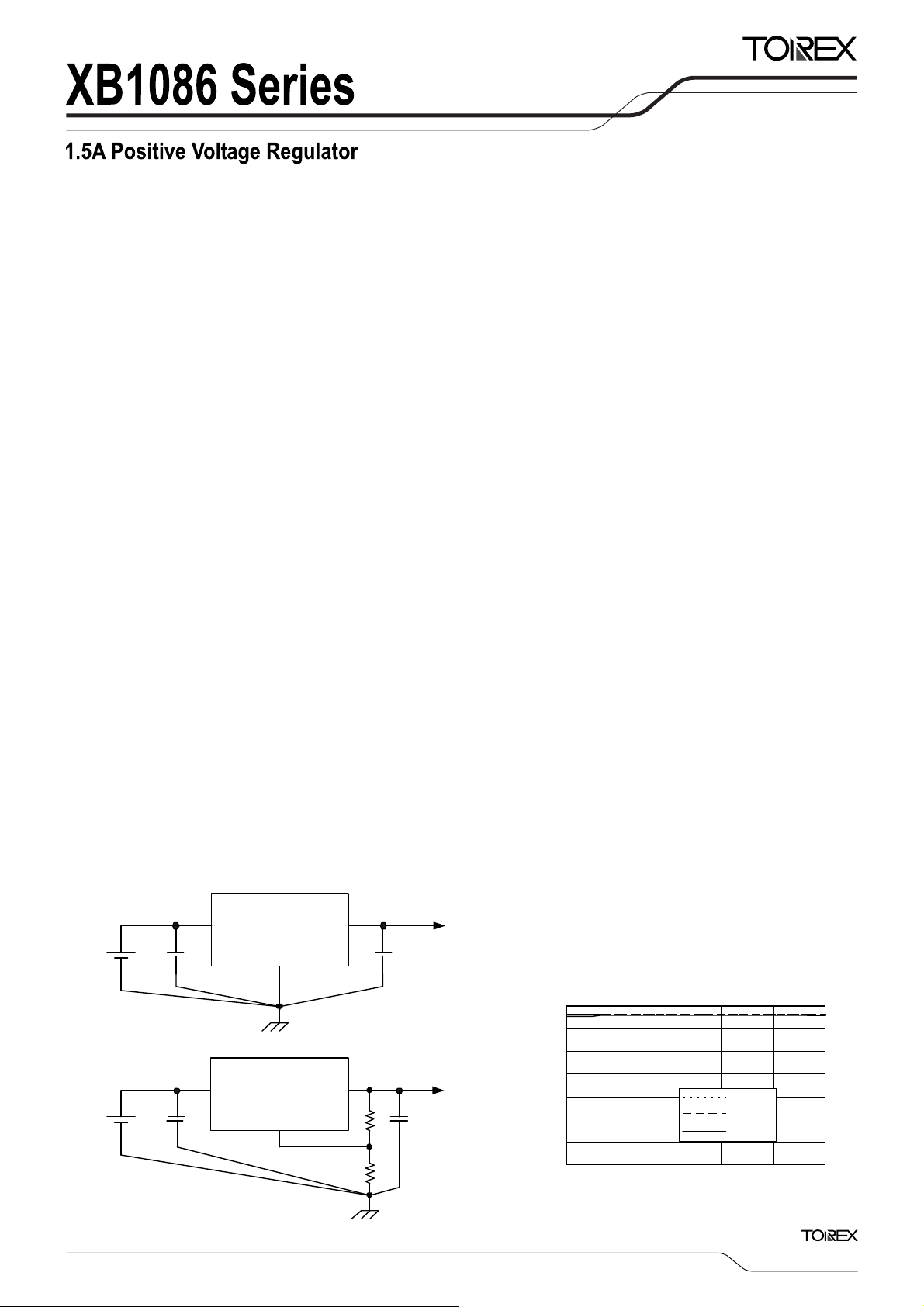
■TYPICAL APPLICATION CIRCUITS
VIN
VIN VOUT
CIN=10μF
CIN=10uF
(Tantalum)
XB1086P Series
VSS
VIN
CIN=10uF
CIN=10μF
XB1086K Series
VIN VOUT
ADJ
(Tantalum)
VOUT=VREF×(1+R2/R1) + IADJ×R2
ackage.
CL=22μF
CL=22uF
(Tantalum)
R1
R2
IOUT
IOUT
CL=22μF
CL=22uF
(Tantalum)
■FEATURES
Maximum Output Current
Maximum Operating Voltage
Output Voltage
Output Voltage Accuracy
Dropout Voltage
Line Regulation
Load Regulation
Reference Voltage Pin Current
Overcurrent Protection Circuit Built-In
Thermal Protection Circuit Built-In
Package
Environmentally Friendly
: More than 1.5A (within Pd)
: 15V
: 1.5V, 1.8V, 2.5V,
3.3V, 5.0V (XB1086P),
Externally Set
(XB1086K / Reference
Voltage 1.25V (TYP.))
: ±1% ( Tj =25℃)
: 1.3V @ I
=1.5A (TYP.)
OUT
: 0.015% (TYP.) <ADJ>
: 0.1% (TYP.) <ADJ>
: Less than 120μA <ADJ>
: TO-252
: EU RoHS Compliant
■TYPICAL PERFORMANCE
CHARACTERISTICS
●Output Voltage vs. Output Current
XB1086P331
VIN=4.9V
CIN=10μF (Tantalum), CL=22μF (Tantalum)
3.5
3.0
2.5
2.0
1.5
1.0
0.5
Output Voltage: VOUT(V)
0.0
0 300 600 900 1200 1500
Output Current: IOUT (mA)
CIN=10uF(Tantal)、CL=22uF(Tantal)
Ta=85℃
Ta=25℃
Ta=0℃
VIN=4.9V
1/11
XB1086 Series
■PIN CONFIGURATION
VSS/
■PIN ASSIGNMENT
PIN NUMBER
TO-252
1 V
2 V
3 VIN Input
■PRODUCT CLASSIFICATION
●Ordering Information
XB1086①②③④⑤⑥-⑦
DESIGNATOR DESCRIPTION SYNBOL DESCRIPTION
① Type of Regulators
②③④
Output Voltage and Output
⑤⑥-⑦
(*1)
The “-G” suffix indicates that the products are Halogen and Antimony free as well as being fully RoHS compliant.
V
OUT
VOUT
(Tab)
(Tab)
2
4
2
2
V
OUT
VOUT
1
13
/
V
SS
ADJ
ADJ
3
V
VIN
IN
TO-252
(TOP VIEW)
PIN NAME FUNCITONS
/ ADJ Ground / Reference Voltage
SS
Output
OUT
(*1)
P Fixed V
K Adjustable (Externally Set)
Voltage Accuracy
Package
(Oder Unit)
151 V
181 V
251 V
331 V
501 V
12B V
JR TO-252 (2,500/Reel)
JR-G TO-252 (2,500/Reel)
=1.5V (±1%)
OUT
=1.8V (±1%)
OUT
=2.5V (±1%)
OUT
=3.3V (±1%)
OUT
=5.1V (±1%)
OUT
=1.25V (±1%)
REF
OUT
2/11
A
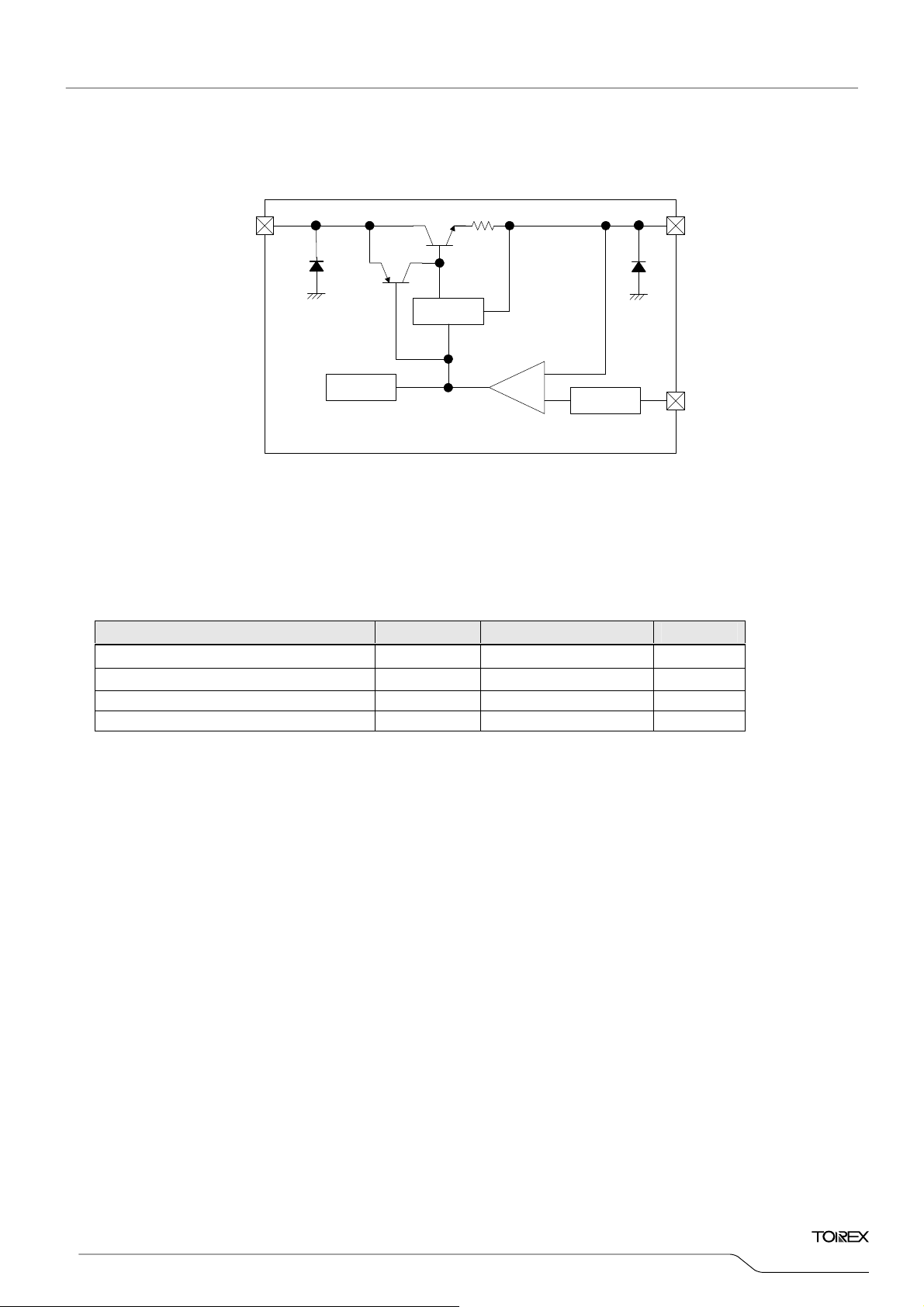
■BLOCK DIAGRAM
■
BSOLUTE MAXIMUM RATINGS
*Diodes inside the circuit are ESD protection diodes.
Thermal
Protection
Current
Limit
Error
Amp
Bandgap
Reference
PARAMETER SYMBOL RATINGS UNIT
Input Voltage VIN 18 V
Power Dissipation
Pd 1300
(*2)
mW
Operating Junction Temperature Tj 125
Storage Temperature Range T
Note:
*1: Stresses greater than those listed under the above ratings may cause permanent damage to the device.
*2: The rating of the power dissipation is determined when mounted on the PCB.
- 55 ~ 125
stg
VOUTVIN
VSS/
ADJ
℃
℃
XB1086
Series
3/11
XB1086 Series
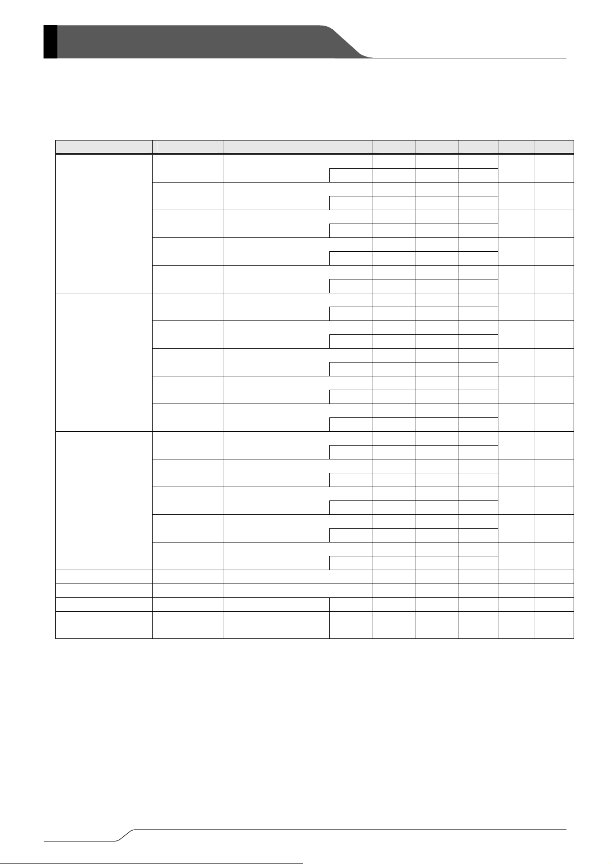
■ELECTRICAL CHARACTERISTICS
XB1086PxxxJ
PARAMETER SYMBOL CONDITIONS MIN. TYP. MAX. UNIT CIRCUIT
1.485 1.5 1.515 VOUT
(*1)
O.T.
1.47 - 1.53
1.782 1.8 1.818 VOUT
(*1)
O.T.
O.T.
O.T.
1.746 - 1.854
(*1)
2.45 - 2.55
(*1)
3.235 - 3.366
4.95 5 5.05
(*1)
O.T.
4.9 - 5.1
- 0.3 6 ⊿VOUT1
(*1)
O.T.
- 0.3 6 ⊿VOUT1
(*1)
O.T.
(*1)
Output Voltage
Line Regulation
IN=3.5V, IOUT=10mA
(1.5V)
(1.8V)
VOUT 2.475 2.500 2.525
(2.5V)
VOUT 3.267 3.300 3.333
(3.3V)
V
OUT
(5.0V)
(1.5V)
(1.8V)
V
VIN=3.8V, IOUT=10mA
VIN=4.5V, IOUT=10mA
VIN=5.0V, IOUT=10mA
VIN=7.0V, IOUT=10mA
1.5V≦V
OUT=10mA
I
1.5V≦V
OUT=10mA
I
IN-VOUT≦10V
IN-VOUT≦10V
⊿VOUT1 1.5V≦VIN-VOUT≦10V - 0.3 6
(2.5V) IOUT=10mA O.T.
⊿VOUT1 1.5V≦VIN-VOUT≦10V - 0.5 10
(*1)
- 0.5 10
(*1)
O.T.
- 3 12 ⊿VOUT2
(*1)
O.T.
- 3 12 ⊿VOUT2
(*1)
O.T.
(*1)
Load Regulation
(3.3V) IOUT=10mA O.T.
⊿VOUT1
(5.0V)
1.5V≦V
OUT=10mA
I
IN-VOUT≦10V
VIN-VOUT=2.0V
(1.5V)
10mA≦I
OUT≦1.5A
VIN-VOUT=2.0V
(1.8V)
10mA≦I
OUT≦1.5A
⊿VOUT2 VIN-VOUT=2.0V - 3 12
(2.5V) 10mA≦IOUT≦1.5A O.T.
⊿VOUT2 VIN-VOUT=2.0V - 3 15
(3.3V) 10mA≦IOUT≦1.5A O.T.
⊿V
OUT2
(5.0V)
VIN-VOUT=2.0V
10mA≦I
OUT≦1.5A
(*1)
- 5 20
(*1)
O.T.
Dropout Voltage Vdif ⊿VOUT=1%, IOUT=1.5A - 1.3 1.5 V ①
IN-VOUT=2.0V
Current Limit ILIM
Supply Current IDD
Temperature Stability
=10mA
I
OUT
Note:
*1: O.T. denotes the specifications which apply over the range of operating junction temperature (0℃≦Tj≦125
Please be sure that the power consumption does not exceed the power dissipation rating, 1300mW. If the power consumption
exceeds the power dissipation rating and the operating junction temperature rises more than the rating, 125
shutdown state.
Ts
O.T.
(*1)
V
VIN=VOUT+1.3V O.T.
V
IN-VOUT=1.5V
OUT=10mA
I
O.T.
(*1)
(*1)
1.5 2.3 - A ①
Tj= 25℃ unless otherwise specified
V ①
V ①
V ①
V ①
V ①
- 0.6 6
- 0.6 6
0.6 6
- 1 10
- 1 10
- 6 20
- 6 20
- 6 20
- 7 20
- 10 35
mV ①
mV ①
mV ①
mV ①
mV ①
mV ①
mV ①
mV ①
mV ①
mV ①
- 5 10 mA ②
- 0.5 - % -
O
C).
O
C, the IC enters thermal
4/11

XB1086
■ELECTRICAL CHARACTERISTICS (Continued)
XB1086K12BJ
PARAMETER SYMBOL CONDITIONS MIN. TYP. MAX. UNIT CIRCUIT
Reference Voltage VREF
Line Regulation ⊿VOUT1
Load Regulation ⊿VOUT2
VIN-VOUT=2.0V 1.238 1.250 1.262
I
OUT=10mA O.T.
(*1)
1.225 - 1.270
1.5V≦VIN-VOUT≦10V - 0.015 0.2
IOUT=10mA O.T.
(*1)
0.035 0.2
VIN-VOUT=2.0V - 0.1 0.3
10mA≦IOUT≦1.5A O.T.
(*1)
0.2 0.4
Dropout Voltage Vdif ⊿VOUT=1%, IOUT=1.5A - 1.3 1.5 V ①
V
Current Limit ILIM
Temperature Stability TS
Minimum Output
Current
Adjust Voltage Pin
Current
Note:
*1: O.T. denotes the specifications which apply over the range of operating junction temperature (0℃≦Tj≦125
Please be sure that the power consumption does not exceed the power dissipation rating, 1300mW. If the power consumption
exceeds the power dissipation rating and the operating junction temperature rises more than the rating, 125
shutdown state.
IOUTmin 1.4V≦VIN-VOUT≦10V O.T.
IADJ
IN-VOUT=2.0V
IN-VOUT=1.5V
V
OUT=10mA
I
VIN=VOUT+1.5V
OUT=10mA
I
1.5 2.3 - A ①
(*1)
O.T.
- 0.5 - % -
(*1)
- 2 5 mA ①
(*1)
O.T.
- 60 120 μA ①
Tj= 25℃ unless otherwise specified
V ①
% ①
% ①
O
C).
O
C, the IC enters thermal
Series
5/11

)
(
XB1086 Series
■TEST CIRCUITS
●XB1086PxxxJ
Circuit ①
Circuit ②
●XB1086K12BJ
Circuit ①
VIN
VIN
VIN
CIN
VIN
V
VOUT
VSS
* CIN=10μF (Tantalum), CL=22μF (Tantalum
A
VIN
VOUT
VSS
VIN
VOUT
ADJ
V
100Ω
A
164Ω
*
※VOUT: 3.3V
* C
IN=10μF
Tantalum), CL=22μF (Tantalum)
A
CLCIN
V
CL
↓
↓
V
6/11

A
■TYPICAL PERFORMANCE CHARACTERISTICS
(1) Output Voltage vs. Output Current
3.5
3.0
2.5
2.0
1.5
1.0
0.5
Output Voltage: VOUT(V)
0.0
0 300 600 900 1200 1500
Dropout Voltage vs. Output Current
(3)
1.4
1.2
1.0
0.8
0.6
0.4
0.2
Dropout Voltage: Vdif (V)
0.0
0 300 600 900 1200 1500
(5) Reference Voltage vs. Ambient Temperature
1.27
1.26
1.25
1.24
1.23
Reference Voltage: VREF (V)
1.22
0 1020304050607080 90
XB1086P331
CIN=10μF (Tantalum), CL=22μF (Tantalum)
CIN=10uF(Tantal)、CL=22uF(Tantal)
Ta=85℃
Ta=25℃
Ta=0℃
Output Current: IOUT (mA)
XB1086P331
CIN=10μF (Tantalum), CL=22μF (Tantalum)
CIN=10uF(Tantal )、CL=22uF(Tantal)
Ta=0℃
Ta=25℃
Ta=85℃
Output Current: IOUT (mA)
XB1086K12B (VOUT=3.3V)
CIN=10μF (Tantalum), CL=22μF (Tantalum)
CIN=10uF(Tantal)、CL=22uF(Tantal)
Ambient Temperature: Ta (℃)
VIN=4.9V
VIN=4.9V
VIN=4.9V
VIN=4.9V
Output Voltage vs. Input Voltage
(2)
3.5
3.0
2.5
2.0
1.5
1.0
0.5
Output Voltage: VOUT(V)
0.0
0246810
(4) Supply Current vs. Input Voltage
6
5
4
3
2
1
Supply Current: ISS (mA)
0
0246 810
(6) Adjust Pin Current vs. Ambient Temperature
XB1086K12B (VOUT=3.3V)
100
80
60
40
20
0
Adjust Pin Curr ent: IADJ (μA)
0 102030405060 708090
Ambient Temperature: Ta (℃)
XB1086P331
IOUT=10mA
CIN=10uF(Tantal)、CL=22uF(Tantal)
CIN=10μF (Tantalum), CL=22μF (Tantalum)
IOUT=10m
Ta=85℃
Ta=25℃
Ta=0℃
Supply Voltage: VIN(V)
Input Voltage: VIN (V)
XB1086P331
CIN=10μF (Tantalum), CL=22μF (Tantalum)
CIN=10uF(Tantal)、CL=22uF(Tantal)
Ta=0℃
Ta=25℃
Ta=85℃
Supply Voltage: VIN(V)
Input Voltage: VIN (V)
IOUT=10mA
CIN=10μF (Tantalum), CL=22μF (Tantalum)
CIN=10uF(Tantal)、CL=22uF(Tantal)
IOUT=10mA
VIN=4.8V
XB1086
Series
7/11

XB1086 Series
■TYPICAL PERFORMANCE CHARACTERISTICS (Continued)
(7) Load Transient Response
2.0
1.6
1.2
0.8
Output Current: IOUT(A)
0.4
0.0
Input Transient Response
(8)
10
9
8
7
6
5
Supply Voltage: VIN(V)
4
Ripple Rejection Rate
(9)
100
80
60
40
20
ripple rejection rate(dB)
Ripple Rejection Rate: PSRR (dB)
0
0.01 0.1 1 10 100
8/11
0.1 1 10
Ripple Frequency: f (kHz)
XB1086P331
CIN=CL=10μF(Tantal)
CIN=CL=10μF (Tantalum)
VIN=4.8V
VOUT
0.75A
IOUT
0.1A
Time(10μs/DIV)
XB1086P331
IOUT=100mA
CIN=1μF (Tantalum), CL=10μF (Tantalum)
CIN=1μF(Tantal),CL=10μF(Tantal)
IOUT=100mA
VOUT
VIN
5.8V
4.8V
Time(20μs/DIV)
XB1086P331
VIN=6.3VDC+1.0Vp-pAC
IOUT=1A, Ta- 25℃, CL=25μF (Tantalum)
IOUT=1ATa=25℃,CL=25μF(Tantal)
VIN=6.3VDC+1.0Vp-pAC
ripple rejection rate(kHz)
VIN=4.8V
3.6
3.4
3.2
3
2.8
2.6
3.32
3.30
3.28
3.26
3.24
3.22
3.20
XB1086K12B (VOUT=3.3V)
CIN=CL=10μF (Tantalum)
CIN=CL=10μF(Tantal)
2.0
1.6
VOUT
1.2
0.8
Output Curr ent:IOUT(A)
Output Vol tage : VOUT(V)
0.4
IOUT
0.0
Time(10μs/DIV)
XB1086K12B (VOUT=3.3V)
CIN=1μF (Tantalum), CL=10μF (Tantalum)
10
CIN=1μF(Tantal),CL=10μF(Tantal)
VOUT
9
8
7
VIN 5.8V
6
Output V ol tage : VOUT(V)
Output Voltage: VOUT (V)
5
Supply Voltage: VIN(V)
4
4.8V
Time(20μs/DIV)
XB1086K12B (VOUT=3.3V)
VIN=6.3VDC+1.0Vp-pAC
VIN=6.3VDC+1.0Vp-pAC
100
IOUT=1A, Ta- 25℃, CL=25μF (Tantalum)
IOUT=1A、Ta=25℃、CL=25μF(Tantal)
80
60
40
20
ripple rejection rate(dB)
0
Ripple Rejection Rate: PSRR (dB)
0.01 0.1 1 10 100
0.1 1 10
ripple rejection rate(kHz)
Ripple Frequency: f (kHz)
VIN=4.8V
VIN=4.8V
0.75A
0.1A
IOUT=100mA
IOUT=100mA
3.6
3.4
3.2
3.0
2.8
2.6
3.35
3.33
3.31
3.29
3.27
3.25
3.23
OutputVoltage:VOUT(V)
Output Voltage: VOUT(V)
Output Voltage: VOUT (V)

■ PACKAGING INFORMATION
●TO-252
0.75±0.15
6.55±0.2
5.3±0.2
0.75±0.15
(2. 28) (2. 28)
0.75±0.15
XB1086
Series
0.5±0.1
1.1±0.25
9.9±0.55
6.1±0.15
0.85±0.25
0. 5±0. 1
+0.1
-0.15
2.3
MIN4.32
単位 : m m
UNIT
9/11

XB1086 Series
■MARKING RULE
●TO-252
① ② ③
④
⑤ ⑥
⑦ ⑧ ⑨
2
1 3
TO-252
(TOP VIEW)
TO252
①② represents product series
MARK
PRODUCT SERIES
① ②
③ represent the type of regulator
④⑤ represents output voltage
8 5 XB1086****J*
MARK PRODUCT SERIES
P XB1086P***J*
K XB1086K***J*
MARK
④ ⑤
1 5 1.5V XB1086P151J*
1 8 1.8V XB1086P181J*
2 5 2.5V XB1086P251J*
3 3 3.3V XB1086P331J*
5 0 5.0V XB1086P501J*
1 2 ADJ XB1086K12BJ*
OUTPUT VOTLAGE
PRODUCT SERIES
⑥ represents output voltage accuracy and output type
OUTPUT VOLTAGE
MARK
1 1% XB1086P**1J*
B ADJ XB1086K12BJ*
ACCURACY
(OUTPUT TYPE)
PRODUCT SERIES
⑦ represents the last digit of production year
ex.)
⑧ represents production lot number
0 to 9, A to Z repeated.
(G, I, J, O, Q, W excepted. ‘0’ of the first digit does not mark.)
*No character inversion used.
ex.)
⑧ ⑨
Blank 3 03
MARK
7 2007
8 2008
MARK
1 A 1A
PRODUCTION YEAR
PRODUCTION LOT NUMBER
10/11

XB1086
Series
1. The products and product specifications contained herein are subject to change without
notice to improve performance characteristics. Consult us, or our representatives
before use, to confirm that the information in this datasheet is up to date.
2. We assume no responsibility for any infringement of patents, patent rights, or other
rights arising from the use of any information and circuitry in this datasheet.
3. Please ensure suitable shipping controls (including fail-safe designs and aging
protection) are in force for equipment employing products listed in this datasheet.
4. The products in this datasheet are not developed, designed, or approved for use with
such equipment whose failure of malfunction can be reasonably expected to directly
endanger the life of, or cause significant injury to, the user.
(e.g. Atomic energy; aerospace; transport; combustion and associated safety
TO-252
equipment thereof.)
(TOP VIEW)
5. Please use the products listed in this datasheet within the specified ranges.
Should you wish to use the products under conditions exceeding the specifications,
please consult us or our representatives.
6. We assume no responsibility for damage or loss due to abnormal use.
7. All rights reserved. No part of this datasheet may be copied or reproduced without the
prior permission of TOREX SEMICONDUCTOR LTD.
11/11
 Loading...