

Page 1

Service Manual
CHASSIS MT35
Contents
1. Caution…………………………………......….…………………...……………2
2. Product Specification………………………..……………………...…….…….6
3. Test and Alignment………………….………………………………...………..9
4. Main IC Brief Instruction
MT5335PU……………………………………....................................................16
MT5133……………………………………........................................................22
MT8295…………………............................................................................…..24
WL6702F………………………………………....….............…..........…………..25
WM8501..........................................................................................................30
SiL9185A.........................................................................................................33
RT8110............................................................................................................47
MP1411...........................................................................................................50
TDA7266.........................................................................................................54
AO4459...........................................................................................................55
13N03LT..........................................................................................................56
5. Block Diagram………………………………….…….. .......................……..57
6. Schematic Diagram……………………………..............................……….58
7. Exploded View
26E90……………………………………………..……….…..............…….…..…86
26E92……………………………………… ...... …………......……................….87
32E90…………………….………………..……….....……..….…..............……..88
32E92..............................................................................................................89
Page 2
CAUTION:
1
Use of controls, adjustments or procedures other than those specified herein may result in
hazardous radiation exposure.
CAUTION: TO REDUCE THE RISK OF
CAUTION
RISK OF ELECTRIC
SHOCK DO NOT OPEN.
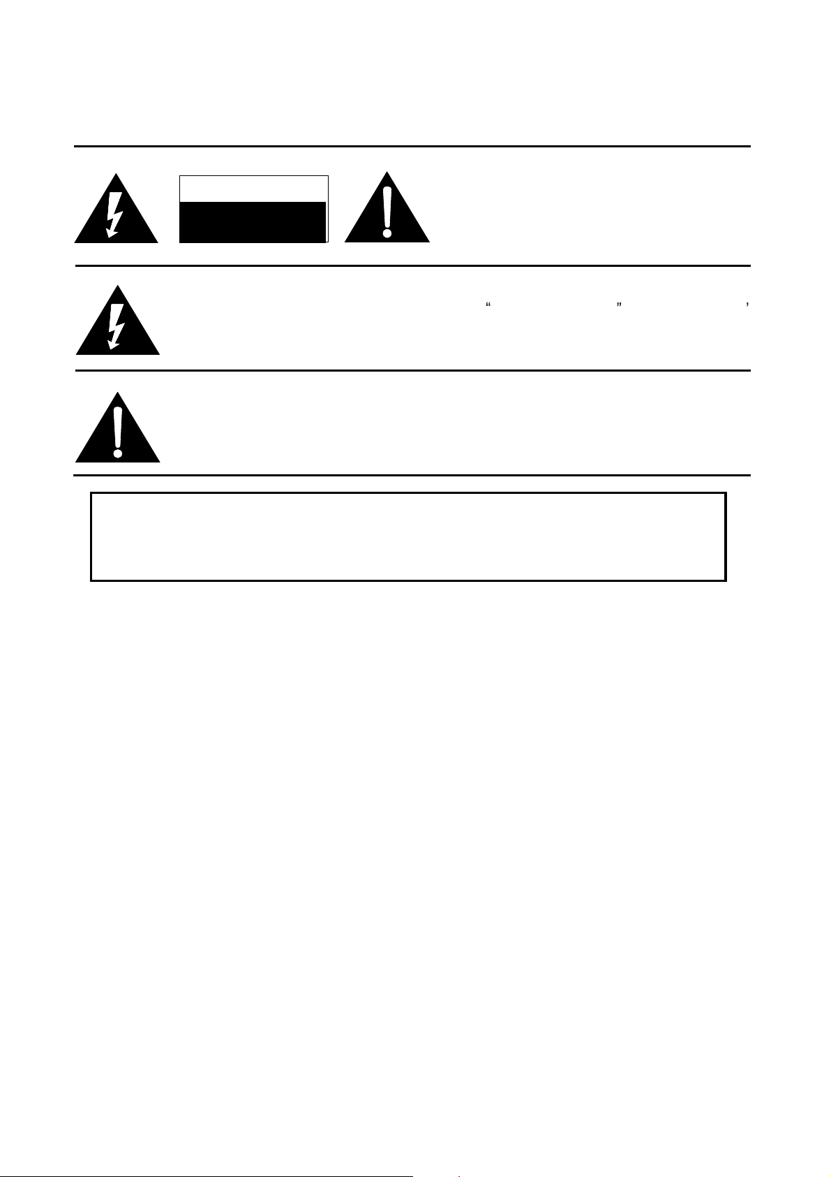
The lighting flash with arrowhead symbol, with an equilateral triangle is intended to
alert the user to the presence of uninsulated voltage within the products
enclosure that may be of sufficient magnitude to constitute a risk of electric shock to
the person.
The exclamation point within an equilateral triangle is intended to alert the user to the
presence of important operating and maintenance (servicing) instructions in the
literature accompanying the appliance.
ELECTRICAL SHOCK, DO NOT REMOVE
COVER (OR BACK). NO USER SERVICEABLE
PARTS INSIDE. REFER SER VICING TO
QUALIFIED SERVICE PERSONNEL.
dangerous
WARNING: TO REDUCE RISK OF FIRE OR ELECTRIC SHOCK, DO NOT
EXPOSE THIS APPLIANCE TO RAIN OR MOISTURE.
2
Page 3

IMPORTANT SAFETY INSTRUCTIONS
CAUTION:
Read all of these instructions. Save these instructions for later use. Follow all Warnings and
Instructions marked on the audio equipment.
1. Read Instructions- All the safety and operating instructions should be read before the product is operated.
2. Retain Instructions- The safety and operating instructions should be retained for future reference.
3. Heed Warnings- All warnings on the product and in the operating instructions should be adhered to.
4. Follow Instructions- All operating and use instructions should be followed.
FOR YOUR PERSONAL SAFETY
1. When the power cord or plug is damaged or frayed, unplug this television set from the wall outlet and refer servicing to
qualified service personnel.
2. Do not overload wall outlets and extension cords as this can result in fire or electric shock.
3. Do not allow anything to rest on or roll over the power cord, and do not place the TV where power cord is subject to
traffic or abuse. This may result in a shock or fire hazard.
4. Do not attempt to service this television set yourself as opening or removing covers may expose you to dangerous
voltage or other hazards. Refer all servicing to qualified service personnel.
5. Never push objects of any kind into this television set through cabinet slots as they may touch dangerous voltage
points or short out parts that could result in a fire or electric shock. Never spill liquid of any kind on the television set.
6. If the television set has been dropped or the cabinet has been damaged, unplug this television set from the wall outlet
and refer servicing to qualified service personnel.
7. If liquid has been spilled into the television set, unplug this television set from the wall outlet and refer servicing to
qualified service personnel.
8. Do not subject your television set to impact of any kind. Be particularly careful not to damage the picture tube surface.
9. Unplug this television set from the wall outlet before cleaning. Do not use liquid cleaners or aerosol cleaners. Use a
damp cloth for cleaning.
10.1. Do not place this television set on an unstable cart, stand, or table. The television set may fall, causing serious injury
to a child or an adult, and serious damage to the appliance. Use only with a cart or stand recommended by the
manufacturer, or sold with the television set. Wall or shelf mounting should follow the manufacturer s instructions, and
should use a mounting kit approved by the manufacturer.
10.2. An appliance and cart combination should be moved with care. Quick stops, excessive force, and uneven surfaces
may cause the appliance and cart combination to overturn.
3
Page 4
PROTECTION AND LOCATION OF YOUR SET
11. Do not use this television set near water ... for example, near a bathtub, washbowl, kitchen sink, or laundry tub, in a
wet basement, or near a swimming pool, etc.
Never expose the set to rain or water. If the set has been exposed to rain or water, unplug the set from the wall
outlet and refer servicing to qualified service personnel.
12. Choose a place where light (artificial or sunlight) does not shine directly on the screen.
13. Avoid dusty places, since piling up of dust inside TV chassis may cause failure of the set when high humidity persists.
14. The set has slots, or openings in the cabinet for ventilation purposes, to provide reliable operation of the receiver, to
protect it from overheating. These openings must not be blocked or covered.
Never cover the slots or openings with cloth or other material.
Never block the bottom ventilation slots of the set by placing it on a bed, sofa, rug, etc.
Never place the set near or over a radiator or heat register.
Never place the set in enclosure, unless proper ventilation is provided.
a built-in
PROTECTION AND LOCATION OF YOUR SET
15.1. If an outside antenna is connected to the television set, be sure the antenna system is grounded so as to provide some
protection against voltage surges and built up static charges, Section 810 of the National Electrical Code, NFPA No.
70-1975, provides information with respect to proper grounding of the mast and supporting structure, grounding of the
lead-in wire to an antenna discharge unit, size of grounding conductors, location of antenna discharge unit, connection
to grounding electrode, and requirements for the grounding electrode.
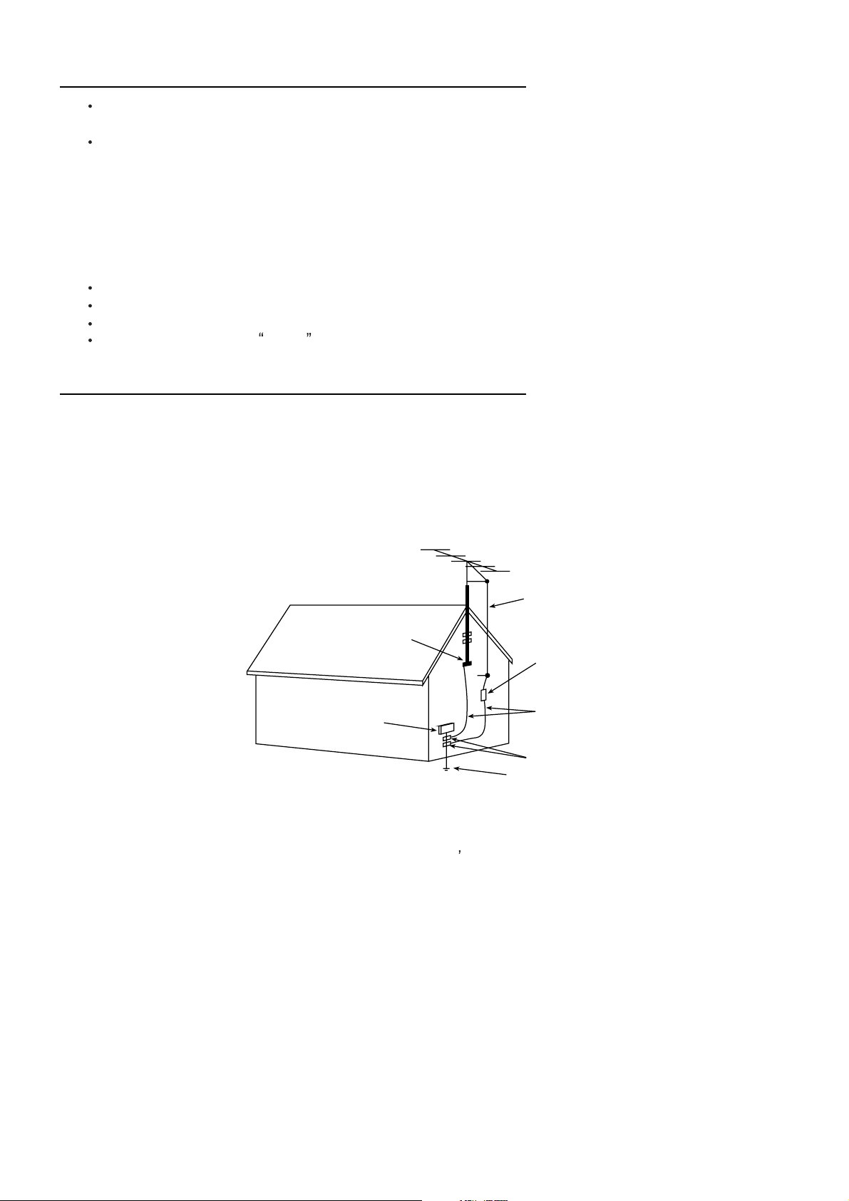
EXAMPLE OF ANTENNA GROUNDING AS PER NATIONAL ELECTRICAL CODE INSTRUCTIONS
EXAMPLE OF ANTENNA GROUNDING AS PER
NATIONAL ELECTRICAL CODE
ANTENNA
LEAD- IN WIRE
GROUND CLAMP
ANTENNA DISCHARGE
UNIT (NEC SECTION
810-20)
GROUNDING
ELECTRIC SERVICE
EQUIPMENT
NEC-NATIONAL ELECTRICAL CODE
15.2. Note to CATV system installer : (Only for the television set with CATV reception)
This reminder is provided to call the CATV system attention to Article 820-40 of the NEC that provides
installer s
guidelines for proper grounding and, in particular, specifies that the cable ground shall be connected to the grounding
system of the building, as close to the point of cable entry as practical.
16. An outside antenna system should not be located in the vicinity of overhead power lines or other electric lights or power
circuits, or where it can fall into such power lines or circuits. When installing an outside antenna system, extreme care
should be taken to keep from touching such power lines or circuits as contact with them might be fatal.
CONDUCTORS
(NEC SECTION810-21)
GROUND CLAMPS
POWER SERVICE GROUNDING
ELECTRODE SYSTEM
(NEC ART 250. PART H)
17. For added protection for this television set during a lightning storm, or when it is left unattended and unused for long
periods of time, unplug it from the wall outlet and disconnect the antenna. This will prevent damage due to lightning
and power-line surges.
4
Page 5

OPERATION OF YOUR SET
18.
This television set should be operated only from the type of power source indicated on the marking label.If you are not
sure of the type of power supply at your home, consult your television dealer or local power company. For television
sets designed to operate from battery power, refer to the operating instructions.
19. If the television set does not operate normally by following the operating instructions, unplug this television set from the
wall outlet and refer servicing to qualified service personnel. Adjust only those controls that are covered in the operating
instructions as improper adjustment of other controls may result in damage and will often require extensive work by a
qualified technician to restore the television set to normal operation.
20. When going on a holiday : If your television set is to remain unused for a period of time, for instance, when you go on
a holiday, turn the television set and unplug the television set from the wall outlet.
off
IF THE SET DOES NOT OPERATE PROPERLY
21. If you are unable to restore normal operation by following thedetailed procedure in your operating instructions,
do not attempt any further adjustment. Unplug the set and call your dealer or service technician.
22. Whenever the television set is damaged or fails, or a distinct change in performance indicates a need for
service, unplug the set and have it checked by a professional service technician.
23. It is normal for some TV sets to make occasional snapping or popping sounds, particularly when being
turned on or off. If the snapping or popping is continuous or frequent, unplug the set and consult your
dealer or service technician.
FOR SERVICE AND MODIFICATION
24. Do not use attachments not recommended by the television set manufacturer as they may cause hazards.
25. When replacement parts are required, be sure the service technician has used replacement parts specified
by the manufacturer that have the same characteristics as the original part. Unauthorized substitutions
may result in fire, electric shock, or other hazards.
26. Upon completion of any service or repairs to the television set, ask the service technician to perform
routine safety checks to determine that the television is in safe operating condition.
5
Page 6
MT35-EU Product Specification
Model # 22E92NH22 26E90NH22 26E92NH22 32E90NH22 32E92NH22
Brand THOMSON THOMSON THOMSON THOMSON THOMSON
Panel technology (LCD / PDP) LCD LCD LCD LCD LCD
Cabinet Design (Example: SC VII, V 6,,,) E9B E9A E9B E9A E9B
PJO Nb 22E92 26E90 26E92 32E90 32E92
EAN Code 3244480284643 3244480284629 3244480284636 3244480284445 3244480284612
Chassis name MT5335 MT5335 MT5335 MT5335 MT5335
Certification(Gostandard/CE/MPTT/…) CE CE CE CE CE
COUNTRIES
France Yes Yes Yes Yes Yes
Germany Yes Yes Yes Yes Yes
Italy, Greece Yes Yes Yes Yes Yes
Spain, Portugal Yes Yes Yes Yes Yes
Benelux (Belgium, Netherland, Luxemburg) Yes Yes Yes Yes Yes
Northern Europe (Sweden, Norway, Denmark,
Finland)
Eastern Europe (Russia, Poland, Czech,
Hungary)
PICTURE
Screen size : diagonale (inch) 22" 26" 26" 32" 32"
Aspect ratio (16/9 // 4/3 // 15/9) 16/9 16/9 16/9 16/9 16/9
Color depth (8/10/12 bits) 8 8 8 8 8
1st panel supplier : panel suppliers AUO CMO CMO LG-Philips LG-Philips
1st panel supplier : panel reference T220SW01 V0 V260B1-L02 V260B1-L02 LC320WXN-SAC1 LC320WXN-SAC1
1st panel supplier : resolution 1680x1050 1366x768 1366x768 1366x768 1366x768
1st panel supplier : pixel Pitch (mmxmm) 0.282x0.282 0.1405x0.4215 0.1405x0.4215 0.17x0.51
1st panel supplier : Horizontal and vertical
viewing angle
1st panel supplier : Typical response time (Grey
to Grey)
1st panel supplier : Typical white luminance
(Nits)
1st panel supplier : Contrast VESA std 1000:1 800:1 800:1 1100:1 1100:1
1st panel supplier : Typical panel Life Time
(Hours)
VIDEO
Noise Reduction (adaptative/…) Yes Yes Yes Yes Yes
Comb Filter (2D/3D) 3D 3D 3D 3D 3D
Deinterlacer (no/linerar/motion adaptive/motion
compensative)
Film mode / reverse 3:2 pull down Yes/Yes Yes/Yes Yes/Yes Yes/Yes Yes/Yes
Format control (Pin8/WSS) Yes/Yes Yes/Yes Yes/Yes Yes/Yes Yes/Yes
Zoom type : 4/3 format Yes Yes Yes Yes Yes
Zoom type : 14/9 Zoom Yes Yes Yes Yes Yes
Zoom type : 16/9 Zoom Yes Yes Yes Yes Yes
Zoom type : 16/9 Zoom up/down Yes Yes Yes Yes Yes
Zoom type : Cinerama Yes Yes Yes Yes Yes
Zoom type : 16/9Format Yes Yes Yes Yes Yes
Colour preset (Cool/Normal/Warm/Favourite) Cool/Normal/Warm Cool/Normal/Warm Cool/Normal/Warm Cool/Normal/Warm Cool/Normal/Warm
Contrast expend (low/medium/high) high high high high high
Picture Reset Yes Yes Yes Yes Yes
Backlight Adjust on factory menu on factory menu on factory menu on factory menu on factory menu
Dynamic Contrast
Picture Autoadjustment (PC mode) Yes Yes Yes Yes Yes
Picture presets : Standard / Film / Studio /
Sport / Personal / Game / Video Camera
Sound
RMS Power (Watt) 2x3W 2x6W 2x6W 2x6W 2x6W
Treble, Bass, Balance, Volume, Mute Control
Sound presets (My
sound/Music/Film/Voice/Flat/Standard/Panoram
a)
Sound techno (Stereo Nicam/Virtual Dolby
Surround/SRS Trusurround XT/BBE Viva/SRS
WoW /…)
Loudspeakers built in (T/M/B) -/2/- -/2/- -/2/- -/2/- -/2/-
Decoding capability
Standard BG/DK/I/LL` BG/DK/I/LL` BG/DK/I/LL` BG/DK/I/LL` BG/DK/I/LL`
Yes Yes Yes Yes Yes
Yes Yes Yes Yes Yes
0.17x0.51
170(H)/160(V) 160(H)/150(V) 160(H)/150(V) 178(H)/178(V) 178(H)/178(V)
5mS 8mS 8mS 8mS 8mS
300 400 400 500 500
50000 50000 50000 50000 50000
Frame buffer Frame buffer Frame buffer Frame buffer Frame buffer
Dynamic Backlight
adjustment
Vivid/Standard
/Movie/ Power
saver/ Personal
Yes/Yes/Yes/Yes/YesYes/Yes/Yes/Yes/YesYes/Yes/Yes/Yes/YesYes/Yes/Yes/Yes/YesYes/Yes/Yes/Yes/Ye
personal/speech/mu
sic/movies/Multimed
ia
NICAM,German
Stereo/AVL/Wide
stereo/Visually
Impaired
Dynamic Backlight
adjustment
Vivid/Standard
/Movie/ Power
saver/ Personal
personal/speech/mu
sic/movies/Multimed
ia
NICAM,German
Stereo/AVL/Wide
stereo/Visually
Impaired
Dynamic Backlight
adjustment
Vivid/Standard
/Movie/ Power saver/
Personal
personal/speech/mu
sic/movies/Multimedi
a
NICAM,German
Stereo/AVL/Wide
stereo/Visually
Impaired
Dynamic Backlight
adjustment
Vivid/Standard
/Movie/ Power
saver/ Personal
personal/speech/mu
sic/movies/Multimed
ia
NICAM,German
Stereo/AVL/Wide
stereo/Visually
Impaired
Dynamic Backlight
adjustment
Vivid/Standard
/Movie/ Power saver/
Personal
s
personal/speech/mus
ic/movies/Multimedia
NICAM,German
Stereo/AVL/Wide
stereo/Visually
Impaired
Page 7

Color System (PAL/SECAM/NTSC)
English\C
h\Ger
DVBT (yes/no) Yes(MPEG 2) Yes(MPEG 2) Yes(MPEG 2) Yes(MPEG 2) Yes(MPEG 2)
Video standard NTSC 3.58 / 4.43 (AV) Yes Yes Yes Yes Yes
HD capability
PC capability (up to maximum format) UXGA UXGA UXGA UXGA UXGA
User convenience
IB languages
Program Numbers (example: 99+3AV)
Number of buttons on cabinet (Power; Vol+/-;
Pr+/-, Menu )
Main switch button (yes/no) No No No No No
Clock Yes Yes Yes Yes Yes
Sleep timer Yes Yes Yes Yes Yes
wake-up timer Yes Yes Yes Yes Yes
Parent Control - Channel lock (Input code for
certain channel)
Parent Control - Child lock (set the lock of the
keyboard, only the RCU can control the TV)
Parent Control - Kid pass (preset the ontime,
channel for each day of the week)
Parent Control - Channel lock (For digital
transmission and DVD program, to filter some
programms)
Program auto switch off Yes Yes Yes Yes Yes
OSD Language*
OSD Positioning No No No No No
OSD Transparency Adjust No No No No No
OSD Timeout Adjust No No No No No
Text Standard: (Top, FLOF,,,) TOP & FLOF TOP & FLOF TOP & FLOF TOP & FLOF TOP & FLOF
Teletext Level: 2.5 / 1.5 1.5 1.5 1.5 1.5 1.5
Pages for teletext 1000 1000 1000 1000 1000
Teletext character sets ****
TV Guide Yes Yes Yes Yes Yes
Auto Naming/Auto Sorting Yes/Yes Yes/Yes Yes/Yes Yes/Yes Yes/Yes
Auto update (for DVBT software ugrades) No No No No No
Multipicture : PIP (Double Tuner) / PIP (AV) /
PAP / PAT / PIC
Hotel mode (Y/N) No No No No No
Tuner FM (yes/no) Yes(in DVB-T) Yes(in DVB-T) Yes(in DVB-T) Yes(in DVB-T) Yes(in DVB-T)
Connectors (if possible, please indicate the
position)
RF Input (Antenna): Analogical / Digital 2 in 1 2 in 1 2 in 1 2 in 1 2 in 1
Scart 1 : CVBS / RGB / S-VIDEO 1/1/- 1/1/- 1/1/- 1/1/- 1/1/CINCH audio in / out (No volumpe control on
Audio out/can be jack 3,5mm)
CINCH video in / out 1(side)/- 1(side)/- 1(side)/- 1(side)/- 1(side)/S-video in / out 1(side)/- 1(side)/- 1(side)/- 1(side)/- 1(side)/-
PAL/SECAM/NTSC(
AV)
YES (720p, 1080i;
1080P 480i/p;
576i/p)
English\Czech\Germ
an\Spanish\Finnish\
French\Greek\Hung
arian\Italian\Dutch\P
olish\Portuguese\Ru
ssian\Swedish\Slova
k\Ukrainian\Estonian
\Latvian\Lithuanian\
Turkish\Norwegian
999+1AV+1SVIDEO
+1CMP+1VGA+2HD
MIs+1SCART
Power, CH +/–, Vol
+/–, Menu
Yes Yes Yes Yes Yes
No No No No No
No No No No No
No No No No No
Bulgarian\Czech\Da
nish\German\Greek\
English\Spanish\Fre
nch\Croatian\Italian\
Hungarian\Dutch\No
rwegian\Polish\Portu
guese\Romanian\Ru
ssian\Slovak\Sloveni
an\Serbian\Finnish\
Swedish\Turkish
Latin Pan-Euro
West
Latin Pan-Euro East
Cyrillic(RussiaBulgarian/Ukrainian/
Byelorussia)
Greek
Arabic
only PAT only PAT only PAT only PAT only PAT
1(side)/- 1(side)/- 1(side)/- 1(side)/- 1(side)/-
PAL/SECAM/NTSC(
AV)
YES (720p, 1080i;
1080P 480i/p;
576i/p)
English\Czech\Germ
an\Spanish\Finnish\
French\Greek\Hung
arian\Italian\Dutch\P
olish\Portuguese\Ru
ssian\Swedish\Slova
k\Ukrainian\Estonian
\Latvian\Lithuanian\
Turkish\Norwegian
999+1AV+1SVIDEO
+1CMP+1VGA+2HD
MIs+1SCART
Power, CH +/–, Vol
+/–, Menu
Bulgarian\Czech\Da
nish\German\Greek\
English\Spanish\Fre
nch\Croatian\Italian\
Hungarian\Dutch\No
rwegian\Polish\Portu
guese\Romanian\Ru
ssian\Slovak\Sloveni
an\Serbian\Finnish\
Swedish\Turkish
Latin Pan-Euro
West
Latin Pan-Euro East
Cyrillic(RussiaBulgarian/Ukrainian/
Byelorussia)
Greek
Arabic
PAL/SECAM/NTSC(
AV)
YES (720p, 1080i;
1080P 480i/p;
576i/p)
English\Czech\Germ
an\Spanish\Finnish\F
rench\Greek\Hungari
an\Italian\Dutch\Poli
sh\Portuguese\Russi
an\Swedish\Slovak\
Ukrainian\Estonian\L
atvian\Lithuanian\Tur
kish\Norwegian
999+1AV+1SVIDEO
+1CMP+1VGA+2HD
MIs+1SCART
Power, CH +/–, Vol
+/–, Menu
Bulgarian\Czech\Dan
ish\German\Greek\E
nglish\Spanish\Frenc
h\Croatian\Italian\Hu
ngarian\Dutch\Norwe
gian\Polish\Portugue
se\Romanian\Russia
n\Slovak\Slovenian\
Serbian\Finnish\Swe
dish\Turkish
Latin Pan-Euro West
Latin Pan-Euro East
Cyrillic(RussiaBulgarian/Ukrainian/
Byelorussia)
Greek
Arabic
PAL/SECAM/NTSC(
AV)
YES (720p, 1080i;
1080P 480i/p;
576i/p)
zec
man\Spanish\Finnis
h\French\Greek\Hun
garian\Italian\Dutch\
Polish\Portuguese\
Russian\Swedish\Sl
ovak\Ukrainian\Esto
nian\Latvian\Lithuan
ian\Turkish\Norwegi
999+1AV+1SVIDEO
+1CMP+1VGA+2H
DMIs+1SCART
Power, CH +/–, Vol
+/–, Menu
Bulgarian\Czech\Da
nish\German\Greek\
English\Spanish\Fre
nch\Croatian\Italian\
Hungarian\Dutch\No
rwegian\Polish\Port
uguese\Romanian\R
ussian\Slovak\Slove
nian\Serbian\Finnish
\Swedish\Turkish
Latin Pan-Euro
West
Latin Pan-Euro East
Cyrillic(RussiaBulgarian/Ukrainian/
Byelorussia)
Greek
Arabic
PAL/SECAM/NTSC(
AV)
YES (720p, 1080i;
1080P 480i/p; 576i/p)
English\Czech\Germ
an\Spanish\Finnish\F
rench\Greek\Hungari
an\Italian\Dutch\Polis
h\Portuguese\Russia
n\Swedish\Slovak\Uk
rainian\Estonian\Latv
ian\Lithuanian\Turkis
h\Norwegian
999+1AV+1SVIDEO
+1CMP+1VGA+2HD
MIs+1SCART
Power, CH +/–, Vol
+/–, Menu
Bulgarian\Czech\Dan
ish\German\Greek\E
nglish\Spanish\Frenc
h\Croatian\Italian\Hu
ngarian\Dutch\Norwe
gian\Polish\Portugue
se\Romanian\Russia
n\Slovak\Slovenian\S
erbian\Finnish\Swedi
sh\Turkish
Latin Pan-Euro West
Latin Pan-Euro East
Cyrillic(RussiaBulgarian/Ukrainian/
Byelorussia)
Greek
Arabic
Page 8
Component Video Input (YCrCb/YPrPb) 1(rear) 1(rear) 1(rear) 1(rear) 1(rear)
Component Audio Input (YCrCb/YPrPb) 1(rear) 1(rear) 1(rear) 1(rear) 1(rear)
VGA in / Audio L/R in / Jack audio in 3.5mm 1/-/1 1/-/1 1/-/1 1/-/1 1/-/1
HDMI1.3 2(1.3) 2(1.3) 2(1.3) 2(1.3) 2(1.3)
DVI-HDCP Share with HDMI Share with HDMI Share with HDMI Share with HDMI Share with HDMI
Audio input for DVI – HDCP share with VGA share with VGA share with VGA share with VGA share with VGA
CINCH subwoofer out / Coaxial out (SP-DIF) -/Yes -/Yes -/Yes -/Yes -/Yes
Headphone connector (mm) 3.5mm,x1 (side) 3.5mm,x1 (side) 3.5mm,x1 (side) 3.5mm,x1 (side) 3.5mm,x1 (side)
RS232 (Y/N) share with VGA share with VGA share with VGA share with VGA share with VGA
USB slot (NO/1.1/2)
Yes(only for SW
update)
Yes(only for SW
update)
Yes(only for SW
update)
Yes(only for SW
update)
Yes(only for SW
update)
DVB-CI (common interface) Yes Yes Yes Yes Yes
Accessories included
Remote control reference RC1994906 RC1994906 RC1994906 RC1994906 RC1994906
Carton (English/French/Spanish) Yes(English) Yes(English) Yes(English) Yes(English) Yes(English)
Batteries Yes Yes Yes Yes Yes
IB Yes Yes Yes Yes Yes
Product registration Card No No No No No
AC power cords 1 1 1 1 1
Audio Cord (Cinch to Jack 3.5mm) No No No No No
VGA Cord No No No No No
Wallmount No No No No No
Antenna Cable No No No No No
General Data
Size (W x H x D, with stand) in mm 529x439x180 663x504x205 663x504x205 796x582x230 796x582x230
Size (W x H x D, without stand) in mm 529x403x73.5 663x461x108 663x461x108 796x535x102 796x535x102
Package Size (W x H x D, with stand but not
mount) in mm
640x520x202 771x548x237 771x548x237 915x652x249 915x652x249
Net Weight in kg 4.9 12 12 15.5 15.5
Gross Weight in Kg 7 14 14 18 18
Power supply 220-240V 50HZ 220-240V 50HZ 220-240V 50HZ 220-240V 50HZ 220-240V 50HZ
Power consumption working / standby / Annual 53W/1W/85KWH 85W/<1W/132KWH 85W/<1W/132KWH
130W/<1W/197KW
h
130W/<1W/198KWh
Design / Mechanical
Wallmount VESA compatible (standard
reference)
VESA compatible VESA compatible VESA compatible VESA compatible VESA compatible
Wallmount VESA Size 100mmx100mm 100mmx100mm 100mmx100mm 200mmx100mm 200mmx100mm
Adaptor for VESA wallmount compatibility
(accessory ref)
No No No No No
Desktop Stand (included/optionnal + ref/NO) Yes Yes Yes Yes Yes
Panel Tilt (Fowards/Backwards/Rotation) No No No No No
Swivel function desktop stand (yes/no) +
motorized?
No No No No No
Docking station (yes/no) No No No No No
Floor Stand (included/optionnal + ref/NO) No No No No No
Glass shield (yes/no) No No No No No
Finish on Front
Finish on side
Finish on back
Finish on stand
HG Spray
paint(Black Q8257)
Black A8252 as
moulded
Black A8252 as
moulded
HG Spray
paint(Black Q8257)
Half translucent as
moulded (high
glossy black)
Black A8252 as
moulded
Black A8252 as
moulded
HG Spray
paint(Black Q0003)
HG Spray
paint(Black Q8257)
Black A8252 as
moulded
Black A8252 as
moulded
HG Spray
paint(Black Q8257)
Half translucent as
moulded (high
glossy black)
Black A8252 as
moulded
Black A8252 as
moulded
HG Spray
paint(Black Q0003)
HG Spray
paint(Black Q8257)
Black A8252 as
moulded
Black A8252 as
moulded
HG Spray
paint(Black Q8257)
number of colors on carton box 1 1 1 1 1
Brand logo THOMSON THOMSON THOMSON THOMSON THOMSON
External AC/DC Power with DC power cord
(yes/no)
Number of Speaker
Rating Label langages
Rating Label Logos/Icons (GOST, Bin,
Recycling, Caution, …)
No/No grounded
plug
2 2 2 2 2
DE, FR, IT, ES, EN,
PL, CS, HU, RU,
PT, EL, NL, SV, DA,
FI, NO
CE, GOST,
Recycling, Class
II,DTB, WEEE bin,
Caution
No/No grounded
plug
DE, FR, IT, ES, EN,
PL, CS, HU, RU,
PT, EL, NL, SV, DA,
FI, NO
CE, GOST,
Recycling, Class
II,DTB, WEEE bin,
Caution
No/No grounded
plug
DE, FR, IT, ES, EN,
PL, CS, HU, RU, PT,
EL, NL, SV, DA, FI,
NO
CE, GOST,
Recycling, Class
II,DTB, WEEE bin,
Caution
No/No grounded
plug
DE, FR, IT, ES, EN,
PL, CS, HU, RU,
PT, EL, NL, SV, DA,
FI, NO
CE, GOST,
Recycling, Class
II,DTB, WEEE bin,
Caution
No/No grounded plug
DE, FR, IT, ES, EN,
PL, CS, HU, RU, PT,
EL, NL, SV, DA, FI,
NO
CE, GOST,
Recycling, Class
II,DTB, WEEE bin,
Caution
Page 9

Test and Alignment Specification for MT35-V0.20
The xxE90/E92NH22 models are Europe LCD platform with DVB-T designed for driving below
panels:
• 32” LPL (LVDS)
• 26” CMO(LVDS)
• 22” AUO(DUAL LVDS)
The main chip is from Mediatec (MTK5335 series) and supports below inputs:
• one analog and digital mixed RF (PAL B/G D/K I, SECAM B/G D/K L/L’,DVB-T)
• one SCART (CVBS & RGB)
• one CMP (YPrPb can support from 480i up to 1080p)
• one VGA
• two HDMI (can support 480i/p, 576i/p, 720p up to 1080i/p)
compliant v1.2. with HDCP, audio included as EIA-861B standard
• one S-Video input
• one Headphone output
• one SPDIF output
More relevant details are listed into the Spec.
INFO:
ª All tests and measurements mentioned hereafter have to be carried out at a normal mains
voltage (110 ~ 240 VAC)
ª All voltages have to be measured with respect to ground, unless otherwise stated
ª All final tests have to be done on a complete set including LCD panel in a room with temperature
of 25+/-7°C
ª The White Balance (color temperature) has to be performed into subdued lighted room after at
least 1 hour of warm-up/burn-in. This is applicable for both Alignment and Picture Performance
evaluation at OQA in order to be set free of any temperature drift (colorimetry vs time)
1. Electrical Assembly Alignment
1.1. Preconditions – DC/DC Check
Before Power On the chassis, please check and make sure that U801,U802,U805, U809, U803,
U804, U811,U201,C817(positive) outputs are not shorted to ground.
Supply 12v and 5v to P804 and test the relative voltage.
position value
U811 3.3V +/-5%
U801 3.3V +/-5%
U802 9V +/-5%
U803 1.2V +/-5%
U804 2.5V +/-5%
U805 5V +/-5%
U809 3.3V +/-5%
Page 10

U201 2.6V +/-5%
C817(+) 1.19V +/-5%
Download latest release MCU_SW into the Standby CPU(U810) using WT_MCU_ISP SW tool. See
Appendixn “How to download MCU SW”.
Download latest release SW into the flash using MTK SW tool. See Appendixo
“How to download
FLASH SW”. Or download the SW from USB port.
1.2. Functional Test
Once the boards (chassis, FAV, KB, IR, PSU…) and the panel are well interconnected, connect all
external generator devices to relevant inputs/outputs below according to their respective test
patterns format and check picture content and sound quality accordingly:
Source Test signal (generator) Test pattern (format/image)
Analog /Digital Tuner RF cable Full Band (VHF/UHF) + CATV DVB-T
SCART1 (CVBS) Chroma/Fluke PAL Half Color & Gray bars
Side av (cvbs)–
Chroma/Fluke PAL Half Color & Gray bars
SVideo(Y/C)
SCART1 (RGB) Chroma/Fluke Half Color & Gray bars
SCART1 (CVBSOut) RF cable First channel
HDMI DVD with HDMI
Movie 720p@60Hz
compliancy
VGA Chroma/QuantumData 1024x768@60Hz
Half Color & Gray bars
Headphone RF cable First channel
Loud Speakers RF cable First channel
CMP (YPrPb) Chroma/QuantumData 1080i@60Hz
Half Color & Gray bars
Audio tones can be defined by the factory (ie: 1KHz & 3KHz, sweep, …).
Picture video formats can be changed by the factory according to their own standard.
1.3. ADC Calibration
Two inputs require an ADC calibration for the time being, That are:
VGA
Provide a test signal 1024×768@60Hz with White Black squares.
Select the corresponding “Auto Color” submenu item from “Factory Menu”, then press ”OK” to
start.
When VGA channel is aligned, SCAR T-RGB is also aligned, so it is not necessary for RGB to be
separately aligned.
CMP
Provide a test signal 576i@50Hz with 100% 8 steps Color Bar.
Select the corresponding “Auto Color” submenu item from “Factory Menu”, then press ”OK” to
start.
Page 11

The ADC is well performed when it’s displayed “CMP” after few seconds.
1.4. DDC & EDID Test
The E-EDID data structure are according to VESA Enhanced EDID 1.3 (and EIA/CEA-861B for
HDMI).
Both VGA and HDMI have their own separate bin files:
For EDID check, it’s needed to check whether the correct EDID is downloaded by checking
corresponding EDID NVM Checksum or read them out to check bit by bit if it is in line with the
released EDID bin file.
• **Before check the EDID please ensure the “Factory Key” in factory menu is disabled
1.5. HDCP Test
For HDCP compliancy, it’s needed to check whether the HDCP key has been well set.
2. Final Assembly Alignment
2.1. Entering to “Factory Menu”
To enter into Factory Menu in case of “Factory Key” is disabled, please to follow below steps:
- press Remote Control key “MENU” to display main menu
- press the subsequence Remote Control keys “7”, “9”, “1” and “5”
- press Remote Control key “MENU” to exit main menu
- press Remote Control key “MENU” to display main menu again
The main menu will display ”FACTCORY” at the last item
To pop-up Factory Menu in case of “Factory Key” is enabled, please to follow below step:
- press Remote Control key “Blue”
To enable/disable “Factory Key”, please to follow below steps:
- press Remote Control “OK” key to enter into “System” submenu
- press Remote Control “RIGHT ”or “LEFT” key till “Factory Key” item
- press Remote Control “OK” key to toggle mode
To exit “Factory Menu”, press “Exit” key from Remote Control.
To comeback to “Factory Menu” root when you are into a submenu:
- press Remote Control “RED” key.
Entering to “P” Mode
2.2.
To enter into “P” mode, an external serial 3.3VDC device is required for sending relevant
commands. See appendixp
“Serial Command Protocol for MTKxx”.
2.3. White Balance Alignment
Only VGA input requires color temperature adjustment as all other inputs or relative ones. Both
Warm and Cool Color Coordinates are also relatives to Normal Color Temperature mode ones.
See appendixq
“CVBS/RGB/CMP/HDMI Relative Matrix Offsets” and “WARM/COOL Relative
Page 12

Matrix Offsets”. Those offsets values don’t require any alignment but can be fine-tuned in Factory
Menu as well.
<The appendix is just a template, Every lot the relative offset is different. We need to align 5 sets
first to get the relative offset data every lot. >
Expected Targets and Tolerances
The measured parameters should be “x, y” coordinates.
The White Balance alignment should be performed using a contact less analyzer (ei: Minolta
CA-210). The analyzer may not touch the screen surface, and measurement must be performed in
a dark environment keeping the probe(s) at 90+/-2° from the panel.
The alignment has to fulfill the requirements in Application Form.
2.4. High Pot. and Insulating Resistance Tests
At the end of the process, a High Pot. and an Insulating Resistance tests are required for
matching Safety Electrical requirements (ei: xxxx)
High Voltage Withstanding requirements
- “Voltage” Ö 4240 VDC
- “Max Leakage Current” Ö 1 mA
- “Test Time” Ö 3 sec
Insulating Resistance requirements
- “Voltage” Ö DC500V
- “Threshold Max” Ö
- “Threshold Min” Ö 4MΩ
- “Test Time” Ö 3 sec
3. “Factory Menu” Definition
1). System
Item Sub-item
Factory Key OFF:Factory Key is invalidation
ON :Factory Key is availability, and BLUE key is the shortcut key.
Note: option step
1)Enter menu
2)7915
3)Exit/Enter menu
4)Enter Factory Item
Enter Factory menu .(Or Enter Factory mode by hotkey )
Burning Mode Off/On
Power Mode Boot/Standby/Previous
Boot: Enter power on mode
Standby: Enter standby mode
Page 13
Pre- frequency
table
Reset
TECI command
2). Balance
Item Sub-item
Balance
Source For balance source
Tone Normal/Warm/Cool
Auto Color
White R R White balance
White G G White balance
White B B White balance
Gray R R Gray balance
Gray G G Gray balance
Gray B B Gray balance
3).Sound Volume Curve
Item Sub-item
Sound
VOL_0 0
Previous: power on according to last status
HuiZhou/ Poland
Note:Pre-Frequency table(HuiZhou/ Poland)
Reset EEPROM data, and load the default value of EEPROM
All: clear NVM values,and set to default value。
User: Clear date of NVM in user menu, except the value of
language / related installation/Factory setting, then set to the
default value.
Shop: Clear date of NVM in user menu, include the val ue related
installation, and Clear date of factory menu except the item
of Balance and sound ,set to default value
Note:Priority below basic function of Factory menu
Note:Switch SOURCE used left/right key
Note: RGB gain range is 0-255
The value of Warm and cool is the
offset of Normal mode, their range is
-128-127, if the offset value beyond
the boundary,set to max or min
value.
Note:display the completed source name
on the right of item,If all the sourcs is
ok ,show “All”
VOL_10 2
VOL_50 14
VOL_90 135
VOL_100 255
Note:mapping volume value
to 0—255 of the MCU
register
Page 14
TV Pre 186
AV Pre 186
4).INFO SW version information
Info
Project LCD_5335_TCL
MTK Version XXXXXX
Version IDTV-XXXXXX_XX
DATE 2008-XX-XX
5).Factory default settings
Followed as OOB setting.
Appendix n
“How to download MCU SW”
Prepare WT_MCU_ISP SW tool for update.
1. Connect the PC to board using MCU updating tool on P802 connector form chassis board.
2. Provide the +5VDC on P804 connector form chassis board and check U811 output voltage
should be 3.3V.
3. Start “WT_MCU_ISP.exe” and download the MCU SW. ( please see file
ISPToolGuideV33-08-2-17)
Appendix o
“How to download FLASH SW”
Prepare MTK SW tool for update.
1. Connect the PC to the board using an external +3.3VDC serial device (USB or COMx) on
P201 connector from chassis board. VGA input can also be used using pin12 (RXD) & pin15
(TXD) just taking care that “Factory Key” from Factory Menu is enabled.
2. Provide the +5VDC STB on P804 connector from chassis board
3. Start “MTKTOOL.exe” application under MTKxx folder, and set the parameters as below
picture:
Page 15

4. Press “Browse” button to select the corresponding SW bin file to upload
5. Press “Upgrade” button to start downloading the SW and wait the gauge displayed “100%”
that means the SW has been successfully downloaded.
In the meanwhile, all operations such erasing flash and so… are parsed into the debug
window script.
6. Once the SW is downloaded, switch-off/on the chassis board and wait few seconds for
Eeprom update.
Appendix p
“Serial Command Protocol for MTKxx”
1. A serial protocol for driving MTK µchip through external +3.3VDC serial device (USB or
COMx) is available. It may facilitate manufacturing process. Thus, both P201 connector from
chassis board or either VGA input can also be used using pin12 (RXD) & pin15 (TXD) just
taking care that “Factory Key” from Factory Menu is enabled.
2. The required serial port settings are as below
• 115200 bps
• 8 data bit
• 1 bit stop
• none parity
3. The command format is like hereafter described into BNS representation:
• 0xBB + Command + Data[[..] + ..] + 0xEE
Both 0xBB and 0xEE bytes are mandatory and used as header and footer of the
transmitted frame. Apart from INIT frame that is described further, all sent bytes need to be triggered
before by an additional one as 0x50. So a complete frame might match following one:
• 0x50+0xBB+0x50+Command+0x50+Data[[..]+0x50+..]+0x50+0xEE
4. At first time, it might be required to initialize MTK µchip by using once below INIT command
(without any triggering byte):
• 0x02 + 0x00 + 0x00 + 0x13 + 0x01 + 0x00
5. A none exhaustive list of commands is already available.
Appendix q
“ WARM/COOL Relative Matrix Offsets”
1. These offsets should be done in the production by AOE.
Page 16

MT5335PU Approval Datasheet
DOCUMENT ARE SUBJECT TO CHANGE WITHOUT NOTICE
MTK CONFIDENTIAL, NO DISCLOSURE
GENERAL DESCRIPTION
The MediaTek MT5335PU family consists of a backend decoder and a TV controller and offers high
integration for advanced applications. It combines a transport de-multiplexer, a high definition MPEG-2
video decoder, an MPEG2 audio decoder, an LVDS transmitter, and an NTSC/PAL/SECAM TV decoder
with a 3D comb filter. The MT5335PU enables consumer electronics manufactures to build high quality, low
cost and feature-rich iDTVs.
World-Leading Audio/Video Technology: The MT5335PU family has built-in high resolution and
TM
high-quality audio codec. It includes MediaTek MDDi
de-interlace solution to generate very smooth
picture quality for motions. A 3D comb filter added to the TV decoder recovers great detail for still pictures.
The special color processing technology provides natural, deep colors and true studio quality graphics.
Rich Features for High Value Products: The MT5335PU family enables a true single-chip experience. It
integrates high-quality HDMI1.3, high speed VGA ADC, dual-channel LVDS, and USB2.0 receiver
Reliable Front-end Receiving Capability: Excellent adjacent and co-channel rejection capability grants
customers never miss any wonderful stream. Professional error-concealment provides stable, smooth and
mosaic-free video quality.
Key Features:
An transport demultiplexer
An MPEG2 video decoder
An AC3 audio decoder
Note: All Package are Lead Free
HDMI1.3 receiver
Audio codec
FEATURES
1/14
Page 17

MT5335PU Approval Datasheet
DOCUMENT ARE SUBJECT TO CHANGE WITHOUT NOTICE
Host CPU
ARM 926EJS
8K I-Cache and 8K D-Cache
4K Instruction TCM
JTAG ICE interface
Watch Dog timers
Transport Demultiplexer
Supports a serial or parallel transport stream input
Supports DVB-T, MPEG-2 transport stream input
Supports DES/3-DES/DVB de-scramblers
Up to 8-PID even/odd keys for descrambling
Supports 32 PID filters and 32 section filters
Supports positive/negative/mask section filtering
Supports hardware CRC-32 check
Supports PCR recovery function
Supports a micro-processor for stream process and MPEG start code detection
MPEG2 Decoder
Supports one MPEG-2 HD decoder
MPEG MP@ML, MP@HL and MPEG-1 video standards
2D Graphics
Supports multiple color modes
Point, horizontal/vertical line primitive drawings
Rectangle fill and gradient fill functions
Bitblt with transparent options
Alpha blending and alpha composition Bitblt
Stretch Bitblt
Font rendering by color expansion
YCbCr to RGB color space conversion
Supports off-line scaler
MTK CONFIDENTIAL, NO DISCLOSURE
OSD Plane
Two linking list OSDs with multiple color mode and one of them has scaler
Video Plane
Supports video capture and over scan.
Flesh tone management
Gamma/anti-Gamma correction
Color Transient Improvement (CTI)
2D Peaking
Saturation/hue adjustment
Brightness and contrast adjustment
Black and White level extender
Adaptive Luma/Chroma management
Automatic detect film or video source
3:2/2:2 pull down source detection
The MT5335PU support bob mode de-interlace with excellent low angle image processing.
Arbitrary ratio vertical/horizontal scaling of video, from 1/32X to 32X
Advanced non-linear panorama scaling.
2/14
Page 18

MT5335PU Approval Datasheet
DOCUMENT ARE SUBJECT TO CHANGE WITHOUT NOTICE
Programmable zoom viewer
Progressive or interlace scan output
Supports alpha blending
Dithering processing for flat panel display
Frame rate conversion.
The MT5335PU supports up to 1680x1050 panel and VGA dot-to-dot.
Supports 2 video source PIP/POP feature.
LVDS
MT5335PU supports 6/8/10-bit one–channel or 6/8-bit dual-channel LVDS transmitter, LVDS speeding
up to 75 MHz
Built-in spread spectrum for EMI performance
Programmable panel timing output
CVBS In
On-chip 54 MHz 10-bit video ADC
Supports PAL (B,G,D,H,M,N,I,Nc), NTSC, NTSC-4.43, SECAM
Macrovision detection
NTSC/PAL support 3D comb filter, SECAM supports 2D comb filter
Built-in motion-adaptive 3D Noise Reduction
VBI data slicer for CC/TT decoding
Supports 2-S-Video.
The MT5335PU supports 3-channel CVBS.
Supports SCART connector
VGA In
Supports VGA input up to UXGA 162 MHz
Supports full VESA standards
Component Video In
Supports two component video inputs
Supports 480i / 480p / 576i / 576p / 720p / 1080i / 1080p
Audio line in interface
The MT5335PU support 1-bit line in data (two channels)
HDMI Receiver
Mixed 3 channels of HDMI1.3, data rate can be up to 2.25 GHz
EIA/CEA-861B
CEC
Audio ADC
The MT5335PU supports 8-channel (4 R/L pairs) analog audio input.
MTK CONFIDENTIAL, NO DISCLOSURE
TV audio demodulator
Supports BTSC/EIA-J/A2/NICAM/PAL FM/SECAM world-wide formats
Standard automatic detection
Stereo demodulation, SAP demodulation
Mode selection (Main/SAP/Stereo)
Audio DAC
Four on-chip audio DACs (2 R/L pairs) support R/L channel and subwoofer outputs
DRAM Controller
3/14
Page 19

MT5335PU Approval Datasheet
DOCUMENT ARE SUBJECT TO CHANGE WITHOUT NOTICE
Supports 64 Mb to 512 Mb DDR DRAM devices
The MT5335PU supports 16-bit data bus; address offers up to 64 M bytes space.
Supports DDR1-333, DDR1-400, DDR2-400, DDR2-533, DDR2-667, DDR2-800
Audio DSP
Supports Dolby Digital AC-3 decoding
MPEG-1 layer I/II decoding (DVB)
Dolby Prologic II
Audio output: 7.1ch + 2ch (down mix)
Pink noise and white noise generator
Equalizer
Bass management
3D surround processing with virtual surround
Audio and video lip synchronization
Supports reverberation
Automatic volume control
One SPDIF out
If internal audio DAC is disabled, the MT5335PU supports 1-bit (2-channel) main audio I
interface. Each channel is up to 24-bit resolution.
Flash Interface
The MT5335PU supports two one serial flash
Serial flash interface supports up to 60 MHz clock rate, depending on the spec. of the flash device
(currently 20 MHz at maximum)
Supports on-the-fly decompression from Serial Flash to DRAM
MTK CONFIDENTIAL, NO DISCLOSURE
2
S output
Peripherals
The MT5335PU has one dedicated UART and one shared UART with GPIO.
The MT5335PU has three basic serial interfaces; one is for the tuner, one is the master for general
purpose and the other is the slave for HDMI EDID data.
Three PWMs
IR blaster and receiver
Real-time clock and watchdog controller
1-port USB2.0/1.1 host supports USB mass storage class devices.
Supports five-channel servo ADC.
IC Outline
The MT5335PU is 256-pin LQFP-EPAD Package
3.3V/1.1V and 2.5V for DDR1, 1.8V for DDR2
4/14
Page 20
MT5335PU Approval Datasheet
DOCUMENT ARE SUBJECT TO CHANGE WITHOUT NOTICE
MTK CONFIDENTIAL, NO DISCLOSURE
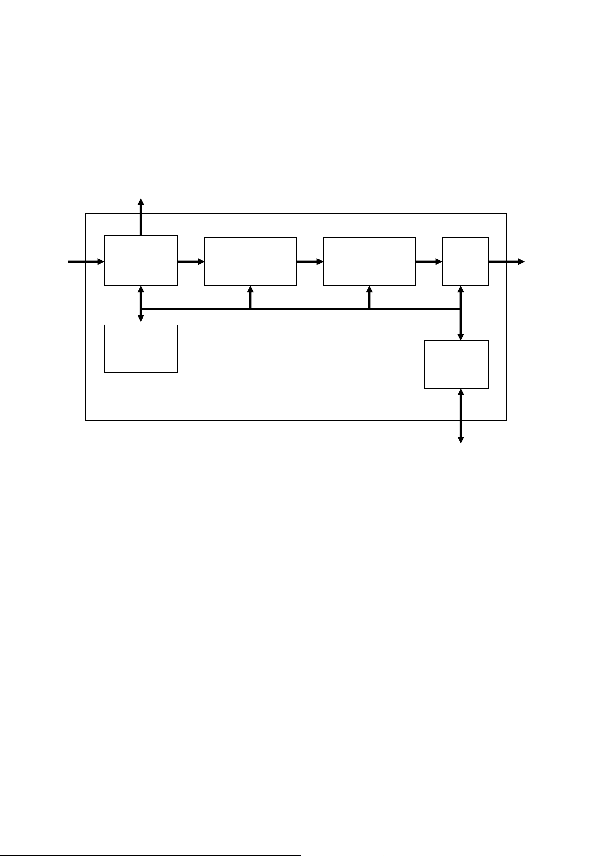
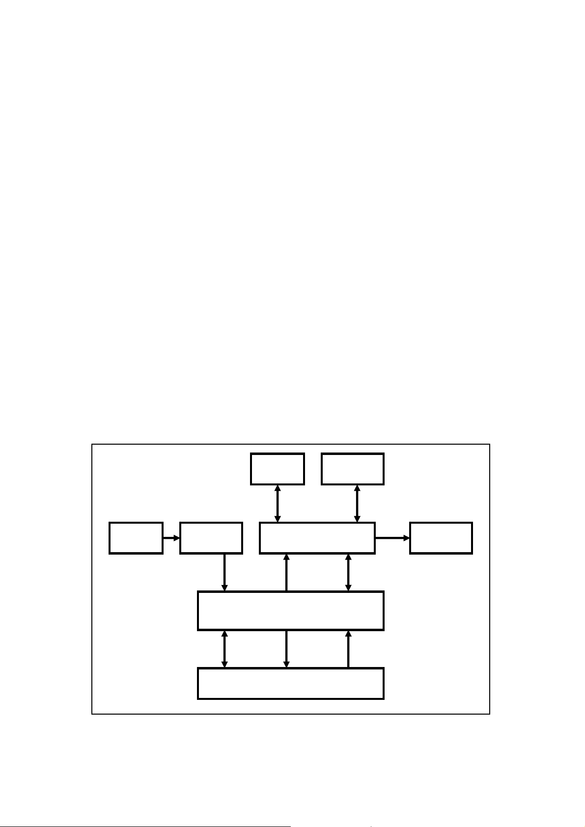
The MT5335PU is designed as an advanced, highly integrated SoC with improved connectivity features
including HDMI interface and component/composite signal connections. Figure 1-1 shows the MT5335PU
system block diagram while Figure 1-2 shows the MT5335PU functional block diagram.
LVDS
LCD
MT5131/3
Tuner
MT 5335P U
DRAMFlash
Pa ne l
Figure 1-1 System Block Diagram
5/14
Page 21
MT5335PU Approval Datasheet
DOCUMENT ARE SUBJECT TO CHANGE WITHOUT NOTICE
TS
In
YC Input
CVBS/
VADCx4
Component
Analog
Input
HDMI
Rx
HDMI In
I/F
Tuner
In
Audio
Demod
TV
Decoder
Audio In
VDO-In
De-interlace
IrDA
Serial IF
JPEG,MPEG
2-D Graphic
USB2.0
Watchdog
ARM
BIM
Audio DSP
TS
Demux
JTAG
Audio I/F
Audio DAC
BScan
PCR MS,SD,SM,xD
RTC
UART
MTK CONFIDENTIAL, NO DISCLOSURE
Audio
Input
Audio
ADC
Panel
LVDS
16-bit DDR
DDR
DRAM
Controller
Mix and Post
Processing
OSD
scaler
Vplane
scaler
DRAM Bus
IO Bus
CKGEN
Serial Flash Servo ADC
PWM
NAND Flash
SPDIF, I
2
S
Figure 1-2 Functional Block Diagram
6/14
Page 22

MT5133 DATA SHEET
General Description
1. Introduction
MT5133 is Media Tak’s 2nd generation COFDM (Coded Orthogonal Frequency
Division Multiplex) channel demodulator for DVB-T receiver. It is fully compliant with
the DVB-T specification (ETSI 300744) and Nordig Unified. MT5133 implements the
functions from tuner IF out to MPEG-2 transport stream input. The device can support
2K, 4K or 8K mode with 6, 7, 8MHz channel. By integrating high performance A/D
converters into the chip, MT5133 can accept first or second IF signal from
conventional tuner thus eliminating the need for an external down-converter. Pure
digital synchronization, advance channel estimation and equalization guarantee the
wide acquisition range of MT5133. User can easily access on-chip information,
including signal-to-noise ratio, Bit Error Ratio (BER) before and after Viterbidecoder.
Serial or parallel MPEG transport stream output can be interfaced to all commonly
available backend processor chips.
2. Features
z ETSI300744 and Nordig Unified compliant
z Suitable for Single Frequency Network (SFN) operation
z Support 2K, 4K, 8K modes
z Support QPSK, 16QAM,64QAM constellations
z 1/4, 1/8, 1/16, 1/32 Guard interval
z Support hierarchical & non-hierarchical modes
z Automatic mode detection
z Full-digital timing/frequency with wide acquisition range
z Support triple offset
z On-chip high-performance 10-bit ADC
z Excellent adjacent Channel interference (ACI) rejection capability
z Excellent Co-Channel interference (CCI) rejection capability
z Build-in PID filters
z Very low power consumption < 180Mw
z Controlled by I2C interface
z Package: QFN48
Page 23
3. Block Diagram
IF
ADC&RF
interface
System
Control
AGC
Time Domain
Processing
Freq. Domain
Processing
FEC
Host
interface
I2C
TSIF
Block Diagram of MT5133
Page 24
MT8295 DATA SHEET
1. Introduction
The MediaTek MT8295 is a companion chip combined with MT533X serial chips to
enable Common Interface (CI) and with the second generation of the Common
Interface (CIV2) functions. It supports DVB compliant Conditional Access Module
(CAM) and PCMCIA type memory cards. A NAND-flash-like bus bridge is built-in to
perform the communication between a host and the card.
Highly Flexible Interface: MT8295 supports one parallel or two serial MPEG2
transport stream interfaces from the front end demodulator and a serial MPEG2
transport stream interface to MPEG2 decoder. Also, the MT8295 is designed with
highly flexible interface timing to compliant with the maximum vendor’s CAMs in the
word.
Extra Value for Your TV: MT8295 enables TV to receive DVB-CI protected program. It
helps content providers to protect their programs and allows customers to receive
more high-value TV programs. Fully tested compliant software is also available for
this device.
2. DTV System Use MT8295
Tuner MT513X MT5335/6/7 Panel
Demod
TS in
CI/PCMCIA
interface
DRAM FLASH
Decoder
TS out
Host
interface
MT8295
Card
TS out
Card
TS in
CAM
Page 25

WT6702F Data Sheet v0.93
1. General Description
The WT6702F is a microcontroller for system power manager with 1)Turbo 8051 compatible (3T) CPU, 2)
8K bytes flash memory, 3) 256 bytes SRAM, 4) 2 PWMs, 5) DPMS detector, 6) 8051 2 timers and UART,
7) Three Slave IIC interface, 8) 4 channel 8-bit A/D converter, 9) Real Time Clock, 10) watch-dog timer,
11) Embedded ISP, 12) Power down mode, 13) Embedded ICE mode.
1.1. Features
Embedded turbo 8051(3T) CPU
• Normal operation mode : 12MHz, 2MHz
• Stand by mode : 32KHz
Memory :
• RAM: 256 Bytes
• Flash memory: 8K Bytes
Turbo 8051 Timer0, Timer1, & UART
Sync processor for monitoring DPMS (VGA connector) wake up signal
8-bit A/D converter with 4 selectable inputs, shared with IO pin
2 PWM pin output
3 slave mode IIC interface
Universal IR Receiver
INT pin to main chip
Watch Dog timer
Low voltage reset
32.768KHz crystal Oscillator & build-in RC Oscillator
Build-in RTC
Maximum 18 programmable IO pins
• 18-IO: 24 pin package
• 14-IO: 20 pin package
• 11/12-IO: 16 pin package
Power consumption :
• Lower than 6mA at 12Mhz mode
• Lower than 4mA at 2Mhz mode
• Lower than 2mA at low speed mode(32KHz)
Operating voltage range : 3.6V – 2.5V
Package:
• SOP16
• SOP20/SSOP20
• SOP24
1.2. Application
• Display system power management MCU with RTC.
• I/O expander with RTC and ADC.
Copyright 2006 Weltrend Semiconductor, Inc. All Rights Reserved.
Weltrend reserves right to modify all information contained in this document without notice.
- 4 -
Page 26

2. Pin Assignment
2.1. Package Type
WT6702F Data Sheet v0.93
32KOSCO
32KOSCI
PWM1/GPIOC1
RXD/IRQ3/GPIOB7
TXD/IRQ2/GPIOB6
HIN/GPIOB5 GPIOB4/VIN
32KOSCO
PWM1/GPIOC1
RXD/IRQ3/GPIOB7
TXD/IRQ2/GPIOB6
HIN/GPIOB5
VIN/GPIOB4
IRQ1/P1.3/GPIOB3
1
2
3
VSS
4
NRST
5
6
7
8 9
1
32KOSCI
2
3
VSS
4
NRST
5
6
7
8
9
10 11
WT6702F_S161
WT6702F_S200
16
VDD
15
GPIOA0/AD0
14
GPIOA3/AD3/IR
13
GPIOA6/SCL1
12
GPIOA7/SDA1
11
GPIOB0/SCL2
10
GPIOB1/SDA2
20
VDD_RTC
19
VDD
18
GPIOA0/AD0
17
GPIOA3/AD3/IR
16
GPIOA4/SCL3/P1.0
15
GPIOA5/SDA3/P1.1
14
GPIOA6/SCL1
13
GPIOA7/SDA1
12
GPIOB0/SCL2
GPIOB1/SDA2
Package Type Package Outline
SOP 16 pin 150mil
SOP 20 pin 300mil
SSOP 20 pin 150mil
SOP 24 pin 300mil
32KOSCO
32KOSCI
VSS
NRST
PWM1/GPIOC1
PWM0/GPIOC0
RXD/IRQ3/GPIOB7
TXD/IRQ2/GPIOB6
HIN/GPIOB5
VIN/GPIOB4
IRQ1/P1.3/GPIOB3
IRQ0/P1.2/GPIOB2
2
3
4
5
6
WT6702F_S240
7
8
9
10
11
12
241
VDD_RTC
23
VDD
22
GPIOA0/AD0
21
GPIOA1/AD1
20
GPIOA2/AD2
19
GPIOA3/AD3/IR
18
GPIOA4/SCL3/P1.0
17
GPIOA5/SDA3/P1.1
16
GPIOA6/SCL1
15
GPIOA7/SDA1
14
GPIOB0/SCL2
13
GPIOB1/SDA2
Copyright 2006 Weltrend Semiconductor, Inc. All Rights Reserved.
Weltrend reserves right to modify all information contained in this document without notice.
- 5 -
Page 27
2.2. Pin Description
WT6702F Data Sheet v0.93
S240 S200 S161
23 19 16
24 20 16 VDD_RTC PWR RTC Power (<3.3V)
1 1 1 32KOSCO O 32kHz oscillator output
2 2 2 32KOSCI I 32kHz oscillator input
3 3 3 VSS GND Ground
4 4 4 NRST I Reset pin, active low (internal pull high)
5 5 5 GPIOC1 I/O PWM1 output. Shared with GPIO C1
6 GPIOC0 I/O PWM0 output. Shared with GPIO C0
7 6 6 GPIOB7 I/O 8051 UART RXD or external IRQ3 interrupt input. Shared with GPIO
8 7 7 GPIOB6 I/O 8051 UART TXD or external IRQ2 interrupt input. Shared with GPIO
9 8 8 GPIOB5 I/O HIN input. Shared with GPIO B5
10 9 9 GPIOB4 I/O VIN input. Shared with GPIO B4
11 10
12
13 11 10 GPIOB1 I/O 2
14 12 11 GPIOB0 I/O 2nd slave IIC SCL2. Shared with GPIO B0
15 13 12 GPIOA7 I/O 1st slave IIC SDA1. Shared with GPIO A7
16 14 13 GPIOA6 I/O 1st slave IIC SCL1. Shared with GPIO A6
17 15
18 16
19 17 14 GPIOA3 I/O Key pad ADC input3 or IR detector input. Shared with GPIO A3
20
21
22 18 15 GPIOA0 I/O Key pad ADC input0. Shared with GPIO A0
GPIOB3 I/O 8051 P1.3 or external IRQ1 interrupt input. Shared with GPIO B3
GPIOB2 I/O 8051 P1.2 or external IRQ0 interrupt input. Shared with GPIO B2
GPIOA5 I/O 3rd slave IIC SDA or 8051 P1.1. Shared with GPIO A5
GPIOA4 I/O 3rd slave IIC SCL or 8051 P1.0. Shared with GPIO A4
GPIOA2 I/O Key pad ADC input2. Shared with GPIO A2
GPIOA1 I/O Key pad ADC input1. Shared with GPIO A1
Pin
Name
VDD PWR Power 3.3V
I/O
B7
B6
nd
slave IIC SDA2. Shared with GPIO B1
Function Description
(a) All GPIOs have Schmitt trigger input.
(b) When use Slave IIC or 8051 P1.x (or UART), the external circuit need pull high(4.7kΩ)
(c) GPIOA3, GPIOA2, GPIOA1, GPIOA0 MAX input are +3.6v(=3.3v+0.3v)
and the other GPIOs MAX input is +5v (5v tolerant PAD)
Copyright 2006 Weltrend Semiconductor, Inc. All Rights Reserved.
Weltrend reserves right to modify all information contained in this document without notice.
- 6 -
Page 28

3. Selection Guide
Part NO. WT6702F_S240 WT6702F_S200 WT6702F_S161
DPMS Detection V V V
UART V V V
8K Flash Memory V V V
RAM 256 Byte V V V
PWM Output 2 1 1
Slave I2C 3 3 2
RTC V V V
IO 18max 14max 11 max
Oscillator
8-bit ADC 4 selectable inputs 2 selectable inputs 2 selectable inputs
Package 24-pin SOP 20-pin SOP/SSOP 16-pin SOP
32KHz Crystal/
RC OSC
WT6702F Data Sheet v0.93
32KHz Crystal/
RC OSC
32KHz Crystal/
RC OSC
Copyright 2006 Weltrend Semiconductor, Inc. All Rights Reserved.
Weltrend reserves right to modify all information contained in this document without notice.
- 7 -
Page 29

4. Functional Block Diagram
Turbo 8031 MCU
WT6702F Data Sheet v0.93
8K bytes code
flash
Internal 256
bytes SRAM
32K Oscillator
RTC
RC
Oscillator
Key Pad ADC
Reset
Processor
Clock
Processor
8051
UART,Timer0,
Timer1
1st SIIC
2nd SIIC
internal bus
3rd SIIC
HV DPMS
Detector
Interrupt
Processor
IR Detector
PWM
Clock off &
Wake Up
4 IRQ
Watchdog
Processor
timer
GPIO
Processor
Copyright 2006 Weltrend Semiconductor, Inc. All Rights Reserved.
Weltrend reserves right to modify all information contained in this document without notice.
- 8 -
Page 30

w
24-bit 192kHz Stereo DAC with 1.7Vrms Line Driver
DESCRIPTION
The WM8501 is a high performance stereo DAC with an
integrated 1.7Vrms line driver. It is designed for audio
applications that require a high voltage output along with
enhanced load drive capability.
The WM8501 supports data input word lengths from 16 to
24-bits and sampling rates up to 192kHz. The WM8501
consists of a serial interface port, digital interpolation filters,
multi-bit sigma delta modulators and stereo DAC in a 14lead SOIC package.
The hardware control interface is used for the selection of
audio data interface format, enable and de-emphasis. The
WM8501 supports I
Operating on separate analog and digital supplies the
WM8501 offers very lower power consumption from the
digital section, whilst supporting enhanced load drive from
the analogue output.
2
S, right Justified or DSP interfaces.
WM8501
FEATURES
• Stereo DAC with 1.7Vrms line driver from 5V analogue
supply
• Audio performance
- 100dB SNR (‘A’ weighted @ 48kHz)
- -88dB THD
• DAC Sampling Frequency: 8kHz – 192kHz
• Pin Selectable Audio Data Interface Format
• 14-lead SOIC package
• 4.5V - 5.5V analogue, 2.7V - 5.5V digital supply operation
APPLICATIONS
• STB
• DVD
• Digital TV
2
- I
S, 16-bit Right Justified or DSP
BLOCK DIAGRAM
WOLFSON MICROELECTRONICS plc
To receive regular email updates, sign up at http://www.wolfsonmicro.com/enews/
Pre-Production, May 2006, Rev 3.1
Copyright 2006 Wolfson Microelectronics plc
Page 31

Pre-Production WM8501
PIN CONFIGURATION
ORDERING INFORMATION
DEVICE
WM8501GED/V -25 to +85oC
WM8501GED/RV -25 to +85oC
Note:
Reel quantity = 3,000
TEMPERATURE
RANGE
PACKAGE
14-lead SOIC
(Pb-free)
14-lead SOIC
(Pb-free, tape and reel)
MOISTURE SENSITIVITY
LEVEL
MSL3
MSL3
PEAK SOLDERING
TEMPERATURE
260°C
260°C
w
PP Rev 3.1 May 2006
3
Page 32

WM8501 Pre-Production
PIN DESCRIPTION
PIN NAME TYPE DESCRIPTION
1
2
3
4
5
6
7
8
9
10
11
12
13
14
Note:
1. Digital input pins have Schmitt trigger input buffers.
LRCLK Digital input Sample rate clock input
DIN Digital input Serial audio data input
BCLK Digital input Bit clock input
ENABLE Digital input Enable input – 0 = powered down, 1 = enabled
VMID Analogue output Analogue internal reference
ROUT Analogue output Right channel DAC output
AGND Supply Ground reference for analog circuits and substrate connection
AVDD Supply Positive supply for analog circuits
LOUT Analogue output Left channel DAC output
DGND Digital Supply Digital ground supply
DVDD Digital Supply Digital positive supply
DEEMPH Digital input De-emphasis select, Internal pull down
High = de-emphasis ON
Low = de-emphasis OFF
FORMAT Digital input Data input format select, Internal pull up
Low = 16-bit right justified or DSP (Mode B)
High = 16-24-bit I
MCLK Digital input Master clock input
2
S or DSP (Mode A)
w
PP Rev 3.1 May 2006
4
Page 33

Silicon Image
Confidential for Philips
Consumer Electronics
Internal Use Only
SiI9185A 3:1 HDMI 1.3 Switch
Preliminary Data Sheet
.
General Description
The SiI9185A is the first generation of TMDS switch device supporting Revision 1.3 of the HDMI Specification (HDMI
Consortium; June 2006). With three HDMI inputs and a single output, the SiI9185A provides a low-cost method of
adding additional HDMI ports to the latest Digital TVs. New DTVs can easily connect to the many HDMI sources
coming on the market, including DVDs, STB, game consoles, PCs, camcorders, and digital still cameras. The SiI9185A
is a fully HDMI compliant device providing a simple, low-cost method of retransmitting protected digital audio and
video, giving end-users a truly all-digital experience. Built-in backward compatibility with DVI 1.0 allows HDMI
systems to connect to any DVI 1.0 source.
The SiI9185A provides additional integrated features to help lower system cost and provide enhanced features to the end
consumer. To lower system cost, the SiI9185A provides a complete solution for switching sink-side HDMI signals. This
includes DDC switching, individual HPD control, and 5V sense. The addition of these features eliminates additional
external components, helping to lower cost. For source-side applications, the SiI9185A DDC switching can be bypassed
with an external 4-channel I
The SiI9185A is the first generation of device from Silicon Image to integrate the Extended Display Identification Data
(EDID). The EDID is stored in on-board RAM that is downloaded from the system microcontroller during power up or
initialization. The EDID is reflected on each of the three HDMI ports through the DDC bus. Flexibility is built in to
allow mixing different EDID formats in an application. This allows elimination of up to three EDID ROMs while also
saving board space.
Finally, the SiI9185A provides a complete, simple solution to enabling Consumer Electronics Control (CEC) in a DTV.
CEC is a single-wire bus that transmits remote control commands throughout a home network. The SiI9185A integrates
both an HDMI-compliant I/O and Silicon Image’s CEC API. The CEC I/O meets all HDMI compliance tests and
eliminates the need for additional external components, again saving board space. The CEC API manages reception and
transmission of all CEC signals according to the CEC protocol and makes the information available to the system
microcontroller. This significantly lowers the system-level control by the system microcontroller, simplifying firmware
overhead.
A very low power standby mode is available, allowing DTVs to meet industry low-power requirements such as Energy
Star. During this mode both the CEC and EDID are still functional.
Silicon Image’s SiI9185A uses the latest generation of TMDS core technology. These TMDS cores are guaranteed to
pass all HDMI compliance tests.
2
C-bus switch (e.g., Texas Instruments PCA95445) to allow clock stretching.
SiI-DS-1016-0.80
© 2007 Silicon Image, Inc. CONFIDENTIAL 1
Page 34

Silicon Image
Confidential for Philips
Consumer Electronics
Internal Use Only
SiI9185A 3:1 HDMI 1.3 Switch
Preliminary Data Sheet
Features
• Three-input, single-output HDMI switch
• Integrated TMDS® receiver and transmitter cores capable of receiving and transmitting 2.25 Gbps:
• Supports video resolutions up to 1080p, 60 Hz, 12-bit or 720p/1080i, 120 Hz, 12-bit
• Built-in adaptive equalizer provides long cable support even at deep-color resolutions
• Pre-emphasis in transmitter
• DVI 1.0, HDCP 1.1 and HDMI 1.3 compliant receiver and transmitter
• Uses HDMI-compliant TMDS core for recovery and retransmission, unlike TMDS switches, which use
high-speed analog switches and degrade TMDS signals
• Built-in Consumer Electronics Control (CEC) support:
• HDMI-compliant CEC I/O simplifies and lowers cost for adding CEC support to DTV
• Integrated CEC API lowers overhead requirements on system microcontroller, speeds design
• Integrated EDID capability to lower system cost
• DDC switching on each input port simplifies board layout and lowers cost
• Individual control of Hot Plug Detect (HPD) for each port
• 5V detect to help speed soft mute of audio during plug-in, plug-out conditions
2
• Control via local I
• Stand-alone mode option:
• Acts as simple switcher
2
• No I
• Low-power standby mode to meet Energy Star and other power saving requirements
• 80-pin QFP package
C control required in this mode
C bus
Silicon Image, Inc.
2 © 2007 Silicon Image, Inc. CONFIDENTIAL SiI-DS-1016-0.80
Page 35

Silicon Image
Confidential for Philips
Consumer Electronics
Internal Use Only
Silicon Image, Inc.
SiI9185A Pin Mapping
I2CSEL/
HPD1
AVCC18
R1XC-
R1XC+
AGND
35
36
37
38
39
40
R1X0–
R1X0+
AVCC33
R1X1–
R1X1+
AGND
R1X2–
R1X2+
AVCC18
DSDA1
DSCL1
RPWR1
CEC_D
CEC_A
AVCC33
HPD2
AVCC18
R2XC-
R2XC+
AGND
41
42
43
44
45
46
47
48
49
50
51
52
53
54
55
56
57
58
59
60
61
62
63
64
65
66
INT
DGND
34
67
DVCC18
33
68
AVCC18
DSDA0
DSCL0
RPWR0
29
30
31
32
80-Pin TQFP
(Top View)
69
70
71
72
R0X2+
28
73
R0X2–
27
74
AGND
26
75
R0X1+
25
76
SiI9185A 3:1 HDMI 1.3 Switch
Preliminary Data Sheet
R0X0–
R0X0+
AVCC33
R0X1–
21
22
23
24
77
78
20
AGND
19
R0XC+
18
R0XC-
17
AVCC18
HPD0
16
LSCL/
15
EPSEL[1]
LSDA/
14
EPSEL[0]
RESET#
13
EXTSWING
12
TxC–
11
10
TxC+
9
AGND
8
Tx0–
7
Tx0+
6
AVCC18
5
Tx1–
4
Tx1+
3
AGND
2
Tx2–
1
Tx2+
79
80
R2X0–
R2X0+
R2X1–
AVCC33
R2X1+
AGND
R2X2–
R2X2+
Figure 1. Pin Mapping
SiI-DS-1016-0.80 © 2007 Silicon Image, Inc. CONFIDENTIAL 3
DSDA2
AVCC18
DSCL2
RPWR2
DVCC18
DGND
TSCL
TSDA
HPDIN
RSVDL
TPWR/
I2CADDR
AGND
Page 36

Silicon Image
Confidential for Philips
Consumer Electronics
Internal Use Only
SiI9185A 3:1 HDMI 1.3 Switch
Preliminary Data Sheet
Silicon Image, Inc.
Functional Description
The SiI9185A provides a low-cost method of providing additional HDMI inputs to a DTV. System cost is reduced by
integrating DDC and HPD switching along with integrated EDID. Feature enhancements like the embedded CEC API
provide a simple method of adding CEC to a DTV without burdening the system microcontroller.
Figure 2 and Figure 3 show the functional blocks of the device as applied to sink and source applications, respectively.
Pin descriptions begin on page 20.
Figure 2. System Architecture, Sink Application
4 © 2007 Silicon Image, Inc. CONFIDENTIAL SiI-DS-1016-0.80
Page 37

Silicon Image
Confidential for Philips
Consumer Electronics
Internal Use Only
Silicon Image, Inc.
SiI9185A 3:1 HDMI 1.3 Switch
Preliminary Data Sheet
Figure 3. System Architecture, Source Application
SiI-DS-1016-0.80 © 2007 Silicon Image, Inc. CONFIDENTIAL 5
Page 38

Silicon Image
Confidential for Philips
Consumer Electronics
Internal Use Only
SiI9185A 3:1 HDMI 1.3 Switch
Preliminary Data Sheet
Silicon Image, Inc.
Block Level Functionality
The SiI9185A 3:1 HDMI 1.3 switch is used to select a single set of HDMI/DVI signals from one of three HDMI/DVI
receiver-ports, and to generate a fully compliant HDMI/DVI stream as an output. It also provides DDC/HDCP, HPD,
and +5V switching to allow full compliance to the HDMI/DVI specifications.
The combination of dynamic equalizer and state-of-the-art DPLL can overcome signal distortion due to the long lengths
of HDMI/DVI cables. SiI9185A-based switches can be cascaded many times to regenerate TMDS and HDCP signals.
Figure 4. Functional Block Diagram
As shown in Figure 4, the SiI9185A consists of five major blocks:
• Receiver block
• Transmitter block
• CEC Interface block
• EDID RAM block
• Configuration block
Receiver Block
The three HDMI/ DVI receive ports are defined as Port 0, Port 1, and Port 2. Each of the ports is terminated separately
and equalized under the control of the receiver digital block and controlled by the local I
power down of all ports are selected by using the Port Select (PSEL[1:0]) signals. PSEL[1:0] can either be controlled by
a register in I
2
The I
HDCP specifications, the SiI9185A also switches and relays information with correct timing from three bidirectional I
Rx-ports to one bidirectional Tx-port. The HDCP switching and relaying operation is also done in the Receive block by
monitoring the I
provide correct HDCP data flow between the selected Receiver and the Transmitter port.
2
C mode, or pins in stand-alone mode.
C Switch conveys bidirectional DDC/EDID and HDCP information. In order to comply with the HDMI/DVI and
2
C/HDCP protocol to decide the right direction of signal transfer. The port selection signal is used to
6 © 2007 Silicon Image, Inc. CONFIDENTIAL SiI-DS-1016-0.80
2
C bus. Port 0, Port 1, Port 2, or
2
C
Page 39

Silicon Image
Confidential for Philips
Consumer Electronics
Internal Use Only
SiI9185A 3:1 HDMI 1.3 Switch
Preliminary Data Sheet
Silicon Image, Inc.
Transmitter Block
The Transmit block consists of a fully compliant, HDMI 1.3 transmitter. This transmitter re-transmits the data received
by the selected receiver port.
CEC Interface
The Consumer Electronics Control (CEC) Interface block provides CEC electrically compliant signals between CEC
devices and a CEC master. It allows products to meet the electrical specifications of CEC signaling by translating the
LVTTL signals of an external microcontroller (CEC host-side or Tx-side) to CEC signaling levels for CEC devices at the
Rx-side, and vice versa.
Additionally, a CEC controller compatible with the Silicon Image CEC API is included on-chip. This CEC controller has
a high-level register interface accessible through the I
commands. This controller makes CEC control very easy and straightforward, and removes the burden of having a host
CPU perform these low-level transactions on the CEC bus.
In order to use the high-level CEC API, the host must perform a calibration of the internal CEC clock inside the
SiI9185A. This calibration is performed by setting the calibration bit, and then sending a 10ms pulse (±1%) on the
CEC_D signal input to the SiI9185A. The SiI9185A uses this pulse to calibrate an internal clock that is then used to
generate all CEC timing to guarantee CEC compliance to the HDMI specification. This calibration must be repeated at
time intervals corresponding to changes in temperature of 15°C.
EDID RAM Block
The EDID RAM block consists of 256 bytes of RAM that is shared by all ports. This means the timing information must
be identical among all the ports if the internal EDID is used. Independent registers for the CEC physical address and
checksum values for each port are also included, as these are unique to each port. On-board logic controls arbitration
when reading the 256 bytes of EDID RAM, CEC physical address, and checksum values. This allows simultaneous reads
of all ports from three different source devices if they are connected and attempt an EDID read at the same time.
The internal EDID can be selected on a per-port basis using registers on the local I
can use the internal EDID, and Port 2 can use a discrete EEPROM for the EDID.
2
C interface which can be used to send and receive CEC
2
C bus. For example: Port 0 and Port 1
Configuration Block
The Configuration block is used to configure and control the operation of the SiI9185A. The SiI9185A has two modes of
operation: I
All of these registers are accessible over the local I
control, CEC control, EDID loading, and power-down control.
In Standalone mode, all functions are controlled and observed by using pins on the SiI9185A. The mode is determined
by the level of the I2CSEL/INT pin at the rising edge of RESET#. A high indicates I
Standalone mode. In Standalone mode, the SiI9185A operates independently, and has no need for an external
microprocessor.
2
C and Standalone. In I2C mode, all functions of the SiI9185A are controlled and observed with I2C registers.
2
C Interface. These registers are used to perform port select, HPD
Figure 5. Standalone Mode Configuration
2
C mode, and a low indicates
SiI-DS-1016-0.80 © 2007 Silicon Image, Inc. CONFIDENTIAL 7
Page 40

Silicon Image
Confidential for Philips
Consumer Electronics
Internal Use Only
SiI9185A 3:1 HDMI 1.3 Switch
Preliminary Data Sheet
Silicon Image, Inc.
2
Figure 6. I
C Control Mode Configuration
I2C Interfaces
There are five I2C interfaces in the SiI9185A. There is one local slave I2C port that is used to configure the operation of
the SiI9185A in I
DDC transmit port; these ports are used to transfer DDC and HDPC information. All of the I
compliant to the I
Local Slave I2C Interface
The local I2C interface on the SiI9185A (pins LSCL and LSDA) is a slave interface capable of running up to 100 kHz.
This bus is used to configure the SiI9185A by reading/writing to necessary registers.
The local I
appear as three separate devices on the I
registers, is fixed, and can only be set to one of two values by using the I2CADDR pin. The other two addresses (used
for CEC and EDID) have an I
so the default value can be changed if there is a bus conflict with another device.
Table 1. Control of the Default I
I2CADDR=LOW I2CADDR=HIGH
PHY and Chip Control Registers (fixed)
EDID Controller (programmable)
CEC Registers (programmable)
The PHY and Chip Control I2C address is fixed at boot-up and cannot be changed. The EDID Controller I2C Address
and the CEC Controller I
the SiI9181/9185 HDMI Switch Programmer’s Reference Guide for more information.
2
C mode. Three slaves are connected to the three DDC receive ports, and one master is connected to the
2
C specification.
2
C interface of the SiI9185A consists of three separate I2C slave addresses. This means the SiI9185A will
2
C register programmable address mapped into the PHY and Chip Control register space,
2
C Address each have a register associated with them that allows the address to be changed. See
2
C local bus. The first of these addresses is used for PHY and Chip Control
2
C Addresses with the I2CADDR Pin
0xD0 0xD4
0xE0 0xE4
0xC0 0xC4
2
C pads are 5V tolerant and
DDC Receiver Ports (Slave) and DDC Transmitter Port (Master) Interfaces
The DDC bus is an I2C interface used in the HDMI interconnection to facilitate bidirectional transfer of DDC/EDID
information and perform the HDCP authentication process between source and sink devices. The SiI9185A includes
three DDC slave I
HDMI transmitters. The SiI9185A also includes a master I
receiver (Figure 3). The DDC ports support I
Standard and supports I
The DDC master I
specification (100 kHz). Due to the relaying function in the SiI9185A, the I
support SCL clock stretching by the slave to which it is connected. This is not an issue when used in sink applications
that use Silicon Image receivers because they do not perform any clock stretching. For other applications it should be
confirmed that the sink receiver device that connects to the SiI9185A output does not perform clock stretching on the I
bus. For source applications an external I
DDC ports of the SiI9185A. This will eliminate the SCL clock stretching issue (see Figure 4).
The SiI9185A will operate between an HDMI source and sink device, so DDC/EDID and HDCP transactions on the
DDC bus must flow through the SiI9185A without causing information loss or timing margin degradation. The SiI9185A
2
C ports, one for each of the receive ports. These are used for direct connection to each of the upstream
2
2
C transactions needed for HDCP.
2
C port and the three DDC slave I2C ports comply with the Standard Mode timing of the I2C
C transactions specified by the VESA Enhanced Display Data Channel
2
C switch (such as the NXP 9545A) can be used to bypass the master and slave
8 © 2007 Silicon Image, Inc. CONFIDENTIAL SiI-DS-1016-0.80
2
C port for direct connection to the downstream HDMI
2
C master in the transmit port does not
2
C
Page 41

Silicon Image
Confidential for Philips
Consumer Electronics
Internal Use Only
SiI9185A 3:1 HDMI 1.3 Switch
Preliminary Data Sheet
Silicon Image, Inc.
analyzes and regenerates the DDC signal, making it possible to extend the cable length of I2C DDC by cascading
multiple SiI9185As together.
Control Pins
The SiI9185A can operate in two distinct modes, depending on the state of the I2CSEL pin at the end of RESET#:
Standalone mode, and I
an external microprocessor. The configuration of the switch is set using signals on the external control pins listed below,
and after configuration, the switch operates independently.
2
C Control mode, the SiI9185A requires an external processor and is controlled over the I2C interface.
In I
RESET# Control Pin
The system reset pin (RESET#) is an active-low input. When RESET# is low, all digital logic is reset including the I2C
interfaces. When RESET# is high, the SiI9185A operates in normal mode.
Two pins are used to configure bootstrap options on the rising edge of RESET#: I2CSEL/INT and I2CADDR/TPWR.
The I2CSEL/INT is sampled on the rising edge of RESET# to determine the operating mode. The I2CADDR/TPWR pin
is sampled on the rising edge of RESET# to determine the base address of the I
the sections that follow.
I2CSEL/INT
The dual-purpose I2CSEL/INT pin acts as a configuration input pin for mode selection during the period when RESET#
is true (low), and as the interrupt (INT) output during normal operation. The level on the I2CSEL/INT pin is latched
when the RESET# signal transitions from low to high. If the I2CSEL/INT value is high on the rising edge of RESET#,
the SiI9185A comes up in I
SiI9185A comes up in Standalone mode and the EPSEL[1:0] pins are used as the external port select pins. Note that
when I2CSEL is low at the rising edge of RESET#, the local I
2
C registers are not lost.
I
After RESET# is deasserted (goes high), the I2CSEL/INT pin becomes the interrupt output pin (INT). When interrupt
conditions are met and the particular interrupt is enabled, the INT signal goes low indicating to the host that an interrupt
has occurred and that actions are needed.
2
C Control mode. In Standalone mode, the SiI9185A operates independently and has no need for
2
C interface. These pins are discussed in
2
C Control mode. If the I2CSEL/INT value is low at the rising edge of RESET#, the
2
C is disabled from that time, but the contents of the local
EPSEL1/LSCL and EPSEL0/LSDA
The EPSEL1/LSCL and EPSEL0/LSDA pins are dual-function pins, and their function depends on whether the
SiI9185A is in Standalone mode or in I
selection pins EPSEL[1:0]. In I
the EPSEL0/LSDA pin becomes the I
The receive port is selected externally using the EPSEL[1:0] pins in Standalone mode, or internally using I
2
C Control mode). When I2CSEL is high at the end of RESET#, the receive port is selected by the I2C register
(I
IPSEL[1:0] (0xD0: 0x08). When I2CSEL is low at the end of RESET#, the receive port is selected using the external
pins EPSEL[1:0] as shown in Table 1, and the local I
Table 2. Port Selection Using the EPSEL Pins
EPSEL1 EPSEL0
Port 0
Port 1
Port 2
Standby Mode
2
0 0
0 1
1 0
1 1
2
C Control mode. In Standalone mode, these pins become the external port
C Control mode, the EPSEL1/LSCL becomes the I2C Interface clock signal LSCL, and
2
C Data signal LSDA.
2
C interface is disabled.
2
C registers
SiI-DS-1016-0.80 © 2007 Silicon Image, Inc. CONFIDENTIAL 9
Page 42

Silicon Image
Confidential for Philips
Consumer Electronics
Internal Use Only
SiI9185A 3:1 HDMI 1.3 Switch
Preliminary Data Sheet
Silicon Image, Inc.
Normal and Standby Modes
There are two power modes: P0 for Normal mode and P1 for Standby mode. The Normal mode, P0, is enabled when one
of three RX ports is selected to provide audio/visual stream and HDCP/DDC information to the TX port as shown in
Table 2. In Normal mode, all power supplies (AVCC33, AVCC18, and DVCC18) must be applied. In P0, all of the
functional blocks are active: PLL, data-paths, local I
Setting PSEL[1:0] = 11 sets the SiI9185A into low-power standby mode (P1). In P1, all of the receive ports transition to
the low-power state and the Tx outputs are disabled (Hi-Z). The purpose of P1 is to make the SiI9185A alive to power
the DDC and CEC interfaces only, while the data-path of the SiI9185A (analog and digital) consumes minimum power.
2
C and DDC relay require logic power (DVCC18), I/O power (AVCC33), and OSC power (AVCC18). Because
The I
none of the receive ports are selected in P1, the PLL does not get an input clock, and shuts itself down. In Standalone
mode P1, the HPD outputs are deasserted (set to 0).
2
C and DDC relaying, and CEC.
I2CADDR/TPWR Control Pin
The I2CADDR/TPWR pin is sampled on the rising edge of RESET# to determine bit two of the default base address for
2
C interface. If I2CADDR/TPWR is low on the rising edge of RESET#, the I2C interface address for the PHY and
the I
Chip Control registers is set to 0xD0, the I
interface address for the CEC Registers is set to 0xC0. If I2CADDR/TPWR is high on the rising edge of RESET#, the
2
C interface addresses are set to 0xD4, 0xE4, and 0xC4, respectively. The actual address values in both modes are
I
shown in Table 1 on page 8.
Once RESET# goes high, the I2CADDR/TPWR pin becomes the normal output Transmit Power (TPWR). TPWR is an
output from the SiI9185A that tells the transmit side that the selected receive port is actually connected. The switching
time between RPWR0/1/2 and TPWR is determined by the PLL lock behavior and logic that detects the presence of a
valid input signal (see RPWR[0:2](+5V) and TPWR(+5V) control pins on page 11 for a description).
2
C interface address for the EDID Controller is set to 0xE0, and the I2C
CEC Transceiver Control Pins
The CEC (Consumer Electronics Control) interface is composed of the bidirectional signals CEC_D, CEC_A, and a
2
C interface. CEC_D is the CEC signal from a CEC Master (microcontroller), and CEC_A is an electrical spec-
local I
compliant CEC signal connected to all CEC Slave devices. The CEC_A signal drives the CEC pins from all three
HDMI/DVI Rx connectors at the same time.
The CEC interface has two modes: CEC_D relay mode and CEC API mode. In CEC_D relay mode, the SiI9185A is
simply a CEC transceiver, and all software must be implemented on the host CPU. In CEC API mode, the SiI9185A
performs all the low-level CEC control, and the host CPU must read and write to high-level I
receive CEC commands. In CEC_D relay mode, the CEC interface only monitors the CEC signal direction and provides
appropriate timing between events. In CEC API mode, the local I
to generate CEC signaling to the CEC_A port, and the local I
HPD Control Pin
The Hot Plug Detection (HPD) signal is provided in the HDMI/DVI connector to provide a signal to the host that the
EDID is readable. In the SiI9185A there are three outputs for the receive side (HPD0, HPD1, and HPD2), and one input
from the transmit side (HPDIN). HPDIN from the Tx port can be relayed to the selected Rx port, or the HPD[0:2]
outputs can be set using registers. In Standalone mode, the HPD outputs of non-selected Rx ports are set to low, so no
EDID transaction or HDCP authentication is initiated for non-selected ports until that port is selected. The default signal
level of the HPD output is low and the high signal level is 3.3V CMOS (and is +5V tolerant).
In internal SiI9185A applications, the HPDIN pin may not to be brought out as an external pin. In this case, the local I
directly controls the HPD output of selected and/or non-selected ports. But in external HDMI switch applications, the
HDMI receiver on the video processing board provides an HPD signal input to the HDMI switch board, and the HPD
input is re-directed to one of the selected receive ports.
2
C Control mode, the state of the HPD pins is controlled by setting the HP_CTRL_x bits in the Hot Plug Detect
In I
Output Control register, where x is the channel number. Each of the HPD0, HPD1, and HPD2 signals is independently
controllable. For example, all three signals could be high at the same time.
HPD output pins have 1-kΩ series resistors integrated to comply with the impedance requirement specified in version 1.3
of the HDMI Specification.
Table 3 on page 11 shows the possible states of the HPD control signals.
2
C registers to send and
2
C provides CEC commands to the CEC interface block
2
C monitors the CEC value in the register map.
2
C
10 © 2007 Silicon Image, Inc. CONFIDENTIAL SiI-DS-1016-0.80
Page 43

Silicon Image
Confidential for Philips
Consumer Electronics
Internal Use Only
SiI9185A 3:1 HDMI 1.3 Switch
Preliminary Data Sheet
Silicon Image, Inc.
Table 3. Hot Plug Control Signal Levels
Condition HPD[2:0] Level
No power to the SiI9185A.
Example: TV unplugged.
SiI9185A out of Reset in I2C
mode
SiI9185A in Standalone mode Pass-through from HPDIN
SiI9185A in I2C mode, register
programming
Port not selected in Standalone
mode
Note that to be HDMI compliant, each HPD Output is ANDed with its respective RPWR input. Hence a given HPD
Output pin can only reflect a High state when the RPWR input of that port detects a High input (and the appropriate
HP_CTRL_ bits are set to 01b, or they are set to 11b with the HPDIN signal being detected as High).
RPWR[0:2](+5V) and TPWR(+5V) Control Pins
The three RPWR (+5V) input signals on the receive side of the SiI9185A (RPWR0, RPWR1, and RPWR2) indicate that
an HDMI cable is connected and 5V is electrically present. The PWR(+5V) signal on the transmit side of the SiI9185A
(TPWR) notifies the receiving device that the transmit port has this 5V present. When the selected receive port is
actually connected to a source device (a DVD player, for example), determined by monitoring the active port’s
RPWR[0:2](+5V) signal, then the transmit port of the SiI9185A sends the receiver-present signal (TPWR) to the HDMI
receiver on the video processing board.
The RPWR(+5V) signal of the selected Rx port, (RPWR0, RPWR1, and RPWR2) is transferred to TPWR under the
control of PSEL[1:0] signals, which can come from registers in I
TPWR signal to the transmit port is pulled low for a period of 1 µS when the port selection is changed. After this time, it
follows the state of the newly selected port.
RPWR input pins have internal pull-down resistors. When a port is not used, simply leaving them unconnected is
sufficient.
Low
Low (default)
Four options: selected by the HP_CTRL_x bits:
0b00 = Low
0b01 = High (3.3V)
0b10 = Tri-state
0b11 = Pass-Through
Low
2
C Control mode, or pins in Standalone mode. The
SiI-DS-1016-0.80 © 2007 Silicon Image, Inc. CONFIDENTIAL 11
Page 44

Silicon Image
Confidential for Philips
Consumer Electronics
Internal Use Only
SiI9185A 3:1 HDMI 1.3 Switch
Preliminary Data Sheet
Silicon Image, Inc.
Embedded EDID
The SiI9185A embeds 256 bytes of RAM for EDID and used to eliminate the discrete EEPROM EDID from the system.
H
D
M
I
0
H
D
M
I
1
H
D
M
I
2
+5V
TMDS0
HPD0
DDC0
CEC_A
+5V
TMDS1
HPD1
DDC1
+5V
TMDS2
HPD2
DDC2
EDID
Select the input and control the SiI 9185
using either SEL0/1 or the I
from the microcontroller
SiI9185A
Optional EDID to
support EDID different
from Port 0 and Port 1
Figure 7. EDID in the SiI9185A
CEC_D
SEL0
SEL1
CSCL/
CSDA
TMDS_Out
DDC_Out
TPWR
HPDIN
2
C interface
Micro-
Controller
Optional 5V
detection output
to Audio DAC
for muting
SiI 9011/
SiI 9013/
SiI 9025/
SiI 9125
EDID Emulation Function
All of the HDMI input ports have a DDC interface consisting of DSDA# and DSCL# where # is the port number. The
SiI9185A device incorporates the function of an HDMI 1.3 compliant EDID in internal registers. The first block must
conform to the VESA EDID specification. The second block must conform to the CEA-861D specification.
The SiI9185A supports two blocks of EDID, each 128 bytes long. Table 4 shows the layout of the EDID block as it
appears to each of the DDC interface controllers.
Table 4. Layout of the EDID Blocks
Block # Description Length DDC I2C Slave
0 EDID 1.3 according to VESA 128 bytes 0xA0 0x00 – 0x7F
1
The host writes the desired information into the EDID memory through the local I2C interface.
EDID extension according to the
CEA 861 specification
128 bytes 0xA0 0x80 – 0xFF
12 © 2007 Silicon Image, Inc. CONFIDENTIAL SiI-DS-1016-0.80
Address
Offset Address
Range
Page 45

Silicon Image
Confidential for Philips
Consumer Electronics
Internal Use Only
SiI9185A 3:1 HDMI 1.3 Switch
Preliminary Data Sheet
Silicon Image, Inc.
EDID Emulation Function Using RAM
The EDID is stored in 256 bytes of on-chip RAM. The SiI9185A contains I2C distributor/arbiter logic to ensure that the
EDID can be read by all three DDC input buses simultaneously.
The EDID memory provides identical information to each DDC channel except for the following:
• The CEC physical address for each channel. The location of this physical address in the EDID memory is
specified by the contents of the CSCPA_ADDR register (0xE0:0x08) in the EDID controller. When the EDID
memory is loaded through the local I
(Port) 0. When the EDID controller detects that DDC for Channel 1 or Channel 2 is trying to read the CEC
physical address location, it automatically replaces the information with the actual CEC1 or CEC2 physical
address values stored in the CEC Physical Channel Address registers.
• Checksum. The checksum is always stored in the last register address for the EDID space (location 0xFF).
When the EDID memory is loaded through the local I
contains the value for Channel (Port) 0. However, the checksum is different for each channel due to the
difference in physical CEC addresses for these channels. The host firmware stores different checksums for
channels 1 and 2 in two different locations in the EDID controller registers. When the EDID controller logic
detects that the DDC for a particular channel is reading the checksum, it responds with the value in one of the
two registers, based on the inquiring port.
Figure 8 shows a block diagram of how the EDID function is emulated using RAM.
2
C controller, the CEC physical address contains the value for Channel
2
C controller, the checksum value (location 0xFF)
Figure 8. EDID Emulation Using RAM
The EDID contains the CEC physical address and must be loaded before enabling the CEC function. Additionally,
HOTPLUG must be controlled to guarantee proper EDID and CEC operation by the host. The basic flow for loading the
EDID into SiI9185A is shown below:
1. Power up the system.
2. Reset the SiI9185A.
3. Load the EDID for Port 0 into the SiI9185A.
4. Write the CEC physical addresses for Port 1 and Port 2.
5. Write the checksum values for Port 1 and Port 2.
6. Calibrate the CEC clock if using the CEC API.
7. Initialize the CEC registers if using the CEC API.
8. Enable DDC and CEC for all ports.
9. Write the registers to set HPD0, HPD1, and HPD2 high (now the host can read the EDID).
SiI-DS-1016-0.80 © 2007 Silicon Image, Inc. CONFIDENTIAL 13
Page 46

Silicon Image
Confidential for Philips
Consumer Electronics
Internal Use Only
SiI9185A 3:1 HDMI 1.3 Switch
Preliminary Data Sheet
Silicon Image, Inc.
CEC API Control
There is hardware assistance in the SiI9185A for CEC control that makes the software development for CEC much
easier. CEC control has been implemented according to the internal Silicon Image CEC API (CPI ) specification.
The CEC signal has two modes of operation:
1. Pass-through mode: In this mode, an external microcontroller can control the CEC level by using the CEC_D
pin. The CEC API function in the SiI9185A is not used.
2. CEC API mode: In this mode, the SiI9185A performs decoding when acting as a follower, and a high-level
command interface when acting as an initiator.
Pass-through mode is engaged under the following conditions:
• When the SiI9185A is working in Standalone mode, or
• When the SiI9185A is working in I
CEC Reference Clock Calibration
An on-chip ring oscillator is used to send and receive CEC data while meeting the CEC timing specification. However,
the ring oscillator frequency can vary on a per device basis, based on manufacturing variables. Therefore, it is necessary
to calibrate this internal ring oscillator by applying an externally driven pulse of 10 ms to the CEC_D pin. The procedure
for applying this calibration signal is:
1. The host processor should set the CEC_D pin high before starting the calibration cycle.
2. The host processor starts the calibration cycle by setting the CALIB bit in local I
bit is self-resetting.
3. The host processor should wait for at least 100 ns after writing the CALIB bit.
4. The host processor should then cause the CEC_D pin to go through a high-to-low transition. The signal should
stay low for a period of 10 ms ±1%, and then transition back high.
5. At this point calibration is complete.
6. The calibration cycle will be repeated each time the host writes a ‘1’ to the CALIB bit.
A counter is used to count the number of ring oscillator clocks in this 10 ms pulse, and the frequency of the ring
oscillator is determined from this count. This is used as the time base to accurately send and receive CEC commands
according to the CEC specification. Note that unless the calibration pulse is properly applied to the SiI9185A and the
calibration cycle is properly completed, the CEC logic will NOT operate correctly. The host should complete the
calibration cycle before setting the CEC enable bit in the local I
The oscillator used in the CEC timing mechanism may vary slightly with temperature. It is recommended that as a
precaution the CEC reference clock calibration process be repeated for every 15°C of change. For example, it may be
periodically recalibrated approximately every 10 minutes.
In standalone applications where CEC-relay mode is used, the incoming CEC timing is measured using the internal
oscillator clock to reproduce the correct output timing. For example, if the START period of CEC_D is measured to be
some number of internal oscillator clocks, that number is used as the basis to re-shape the CEC output timing. Therefore,
in CEC-relay mode a calibration pulse is not required.
2
C Control mode but the CEC enable bit is set to 0 (offset 0x08 bit 6)
2
C offset 0x09 bit 0 to 1. This
2
C.
CEC Programming Interface (CPI)
The CEC application solution involves both low-level and a high-level components. For low-level components, the lowlevel CEC protocol is handled by the slave I
CEC software source code allows command strings to be exchanged over the I
For development, Silicon Image provides Windows-based software tools, including a kit that allows a PC to be used to
generate I
The I
set is used across all Silicon Image devices and applications, both software and hardware.
2
C commands over any USB 1.1-capable port.
2
C register set used for this solution is referred to as CEC Programming Interface or just CPI. This standard register
2
C interface of the SiI9185A. For high-level components, the Silicon Image
14 © 2007 Silicon Image, Inc. CONFIDENTIAL SiI-DS-1016-0.80
2
C interface as discussed above.
Page 47

Conceptual
RT8110
Wide Range Input Voltage Simple Synchronous DC/DC
Converter
General Description
The RT8110 is a single power supply PWM DC-DC
controller designed to drive N-MOSFET in a synchronous
buck topology. The IC integrates the control, output
adjustment, monitor and protection functions in a small
8-pin package.
The RT81 10 uses an internal compensation high DC gain
voltage mode PWM control for simple a pplication design.
An internal 0.8V reference allows the output voltage to be
precisely regulated for low voltage requirement. A fixed
400kHz oscillator reduces the component size for saving
board space.
The RT81 10 features over current protection, a nd under
voltage lock-out. The output current is monitored by
sensing the voltage drop across the Low side MOSFET's
R
, which eliminates the need for a current sensing
DS(ON)
resistor.
Ordering Information
RT8110
Note :
RichTek Pb-free and Green products are :
-
Package Type
V8 : SOT-23-8
Operating Temperature Range
P : Pb Free with Commercial Standard
G : Green (Halogen Free with Commer cial Standard)
`RoHS compliant and compatible with the current require-
ments of IPC/JEDEC J-STD-020.
`Suitable for use in SnPb or Pb-free soldering processes.
`100% matte tin (Sn) plating.
Features
zz
Wide Input Operation Voltage 5V to 23V
z
zz
zz
z 0.8V Internal Reference
zz
zz
z Drive Two N-MOSFET s
zz
zz
z High DC gain Voltage Mode PWM Control
zz
zz
z Fast T ran sient Respon se
zz
zz
z Fixed 400kHz Oscillator Freq uency
zz
zz
z Fully Dynamic 0 to 80% Duty Cycle
zz
zz
z Internal Soft Start
zz
zz
z Adaptive Non-Overlapping Gate Driver
zz
zz
z Over-Current Protection Under Voltage Lockout
zz
zz
z RoHS Compliant and 100% Lead (Pb)-Free
zz
Applications
z Motherboard Power Regulation for Computers
z Subsystems Power Supplies
z Cable Modems, Set Top Boxes, and DSL Modems
z DSP and Core Communication processor Supplies
z Memory Power Supplies
z Personal Computer Peripherals
z Industrial Power Supplies
z 5V-Input DC-DC Regulators
z Low V oltage Distributed Power Supplies
Pin Configurations
(TOP VIEW)
PHASE
GND
UGATE
7
1
2
LGATE
5
68
34
FB
Marking Information
For marking information, contact our sales re presentative
directly or through a RichTek distributor located in your
area, otherwise visit our website for detail.
BOOT
DRIVE
SOT-23-8
Note : There is no pin1 indicator on top mark for SOT-23-8
type, and pin 1 will be lower left pin when reading top mark
VCC
from left to right.
DS8110-01C March 2007 www.richtek.com
1
Page 48

RT8110
Typical Application Circuit
1
C
1uF
Q
R1
k
2
E
n
Chip Shutdown
1
N
2
2
2
2
2
R1
0
1
5
V
2
R2
R2
k
0
1
v
V
h
k
0
C
1uF
1
Q
2
0
0
7
N
2
Conceptual
V
I
D
1
M
A
7
3
2
C
R
T
8
1
1
4
V
C
2
D
R
3
F
B
4
V
C
1
2
D
R
3
F
B
0
C
I
V
E
1
D
M
A
7
R
T
8
C
I
V
E
1
O
B
T
O
7
T
A
G
U
E
8
P
H
A
S
E
5
A
L
G
T
E
6
D
N
G
3
2
1
1
0
1
O
B
T
O
7
T
A
G
U
E
8
P
H
A
S
E
5
A
L
G
T
E
6
D
N
G
2
0.1uF
C
2
0.1uF
N
+
4
C
3
C
1
L
M
U
5
M
L
V
I
N
M
U
5
M
L
4
7
0
u
u
F
1
u
H
R3
2
1
3
C
1
u
F
L
1
u
H
F
V
T
U
+
C
5
1
0
0
0
u
F
6
C
1
0
n
F
R4
5
5
2
0
+
4
C
+
C
5
1
0
0
0
u
6
C
1
0
n
F
O
2
.
5
V
V
T
U
O
2
.
5
V
F
R4
R3
2
1
5
5
2
0
DS8110-01C March 2007www.richtek.com
2
Page 49

Conceptual
Functional Pin Description
Pin No. Pin Name Pin Function
This pin prov ides grou nd ref erenced bi as voltage to the upper MOSFET dri ver. A bootstrap
1 BOOT
2 DRIVE
circuit is used to cr eate a v oltage su itable to drive a logic- level N -MOSF ET when operatin g
at a single 5V power supply.
This pin connects to the base of the external BJT(2N2222), wh ich is designed to withstand
to 23V and provides a regulated 5.3V voltage to VCC pin as the power of the PWM
controller. The pin also can function as shut down with two different application circuits. The
one can pull low the pin to gnd, the other can pu ll low drive to make V
threshold.
RT8110
lower than PO R
DD
3 FB
This pin is connected to the PWM controller’s output divider. This pin also connects to
internal PWM error amplifier inverting input and protection monitor.
This is the m ain bias supply for the RT8110. This pin also pro vid es th e gate b ias c har ge f or
4 VCC
the lower MOSFET gate. The voltage at this pin is monitored for power-on reset (POR)
purpose.
5 LGATE
6
GND Signal and power ground for the IC. All voltage levels are measured with respect to this pin.
7 UGATE
8 PHASE
Connect LGATE to t he PWM controller’s lower MOSFET gate. T his pin provides the gat e
drive for the lower MOSFET.
Connect UGATE pin to the PW M controller’s upper MOSFET gate. This pin provides the
gate drive for the upper MOSFET.
This pin is used to monitor the voltage drop across the lower MOSFET for over-current
protection.
Function Block Diagram
0.8V
REF
SSE
+
Gm
FB
+
-
0.5V
EO
DRIVE
VCC
Regulator
SS
Oscillator
+
+
+
-
VCC
UVP
PWM
Power-
On Reset
POR
Soft-Start
and Fault
Logic
S1L
Gate
Control
Logic
OC
PH_M
VCC
I
OC
R
1.5V
VCC
OC
PHASE
UGATE
BOOT
LGATE
GND
+
-
+
DS8110-01C March 2007 www.richtek.com
3
Page 50

Page 51

Page 52

Page 53

Page 54

Page 55

A
A
AO4459
p
P-Channel Enhancement Mode Field Effect Transistor
General Description
The AO4459 uses advanced trench technology to provide
excellent R
for use as a load switch or in PWM applications. Standard
roduct AO4459 is Pb-free (meets ROHS & Sony 259
specifications). AO4459L is a Green Product ordering
with low gate charge. This device is suitable
DS(ON)
Features
VDS (V) = -30V
I
= -6.5A (VGS = -10V)
D
R
< 46mΩ (VGS = -10V)
DS(ON)
R
< 72mΩ (VGS = -4.5V)
DS(ON)
option. AO4459 and AO4459L are electrically identical.
SOIC-8
Top View
S
S
S
G
Absolute Maximum Ratings T
A
D
D
D
D
=25°C unless otherwise noted
G
Symbol
Drain-Source Voltage -30
Continuous Drain
Current
A
Pulsed Drain Current
B
T
A
T
A
=25°C
=70°C
TA=25°C
Power Dissipation
A
T
=70°C
A
Junction and Storage Temperature Range
V
DS
V
GS
I
D
I
DM
P
D
TJ, T
STG
D
S
Maximum UnitsParameter
±20Gate-Source Voltage
-6.5
-5.3
-30
3.1
2
-55 to 150
V
V
A
W
°C
Thermal Characteristics
Parameter Units
Maximum Junction-to-Ambient
Maximum Junction-to-Ambient
Maximum Junction-to-Lead
C
t ≤ 10s
Steady-State
Steady-State
Symbol Typ Max
R
θJA
R
θJL
33 40
62 75
18 24
°C/W
°C/W
°C/W
Alpha & Omega Semiconductor, Ltd.
Page 56

M3D315
1. Product profile
1.1 Description
1.2 Features
PHKD13N03LT
Dual TrenchMOS™ logic level FET
Rev. 01 — 23 June 2003 Product data
Dual N-channel enhancement mode field-effect transistor in a plastic package using
TrenchMOS™ technology.
Product availability:
PHKD13N03LT in SOT96-1 (SO8).
■ Low gate charge ■ Surface mount package
■ Low on-state resistance ■ Fast switching.
1.3 Applications
■ Portable appliances ■ Notebook computers
■ Lithium-ion battery chargers ■ DC-to-DC converters.
1.4 Quick reference data
■ VDS≤ 30 V ■ ID≤ 10.4 A
■ P
≤ 3.57 W ■ R
tot
DSon
2. Pinning information
Table 1: Pinning - SOT96-1 (SO8), simplified outline and symbol
Pin Description Simplified outline Symbol
1 source1 (s1)
2 gate1 (g1)
3 source2 (s2)
4 gate2 (g2)
5,6 drain2 (d2)
7,8 drain1 (d1)
8
1
Top view MBK187
SOT96-1 (SO8)
5
4
≤ 20 mΩ
d
1
1
d
d
1
gs
1
d
2
2
gs
2
2
MBK725
Page 57

DC-DC
12V to 5V RT8110
VCC
+12V
OFF ON
+5V/
Standby+5v
POWER
SUPPLY CONNECTOR
TUNER_I2C
MT35 BLOCK DIAGRAM V2.0
IF+/IF-
8051 MCU
15 KEY 9 POWERON
11 STANDBY 14 IR
KEY BOARD
FLASH
32Mbit
EEPROM
M24C16MN
Main Chip
152 KEY
93 IR
I2C
TUNER
205 SCL
206 SDA
SAW-Sif
SAW-V if
IF
amplif
ier
132 TV_CVBS
164 SIF
DVB-T
demodulat
or
PARALLEL TS
SERIAL TS
LV
DS
CI function Chip
LVDS
To
TTL
386
TTL
PARALLEL TS
PARALLEL TS
PANEL
CI
CARD
DDR
32Mb
x16
CEC
COMMAND
62 OSCL1 63OSDA1
73 HDMI_5V
79 RX0_CB 80 RX0_C
81 RX0_0B 82 RXO_0
83 RX0_1B 84RXO_1
85 RX0_2B 86 RX0_2
205 DDC_SCL
204 DDC_SDA
HDMI SWITCH
EDID EDID
HDMI1 HDM2
104 R
98 B
102 G
96 VSYNC
97 HSYNC
VGA
EDID
120 Y_IN
121 Pb_IN
123 Pr_IN
173 YPbPr_L
174 YPbPr_R
176 VGA_R
177 VGA_L
YPbPr
170 SCT_R_IN
171 SCT_L_IN
116 SCT_R
108 SCT_G
114 SCT_B
149 SCT_FS
107 SCT_FB
187 SCT_R_OUT
189 SCT_L_OUT
O/P
SCART
201
SPDIF
_OUT
SPDIF
129 CVBS
172 R_IN
173 L_IN
126 SY
125 SC
AV
185
HP_R_OUT
186
HP_L_OUT
LVDS
Broken line is option for TTL
interface panel!
PRE AUDIO
R/L
AMP
HEAD PHONE
AUDIO
AMP
R
L
Page 58

for TCL TQP
8 7 6 5 4 3 2 1
Z100
0.1U
C137
TUNER_5V
5
VCC
F
U101
OUT2
24
SIF2
VIF1
1
23
2
1
SIF1
VIF2
C107
Y
R149
NC\0R
OP2
OP1
390P
ANTPWR
B1
NC/GND1
1
2
3
4
NC/GND2
NC/RFAGC
5
R148
NC
6
0R
RF-AGC
C129
0.1U
TU
111412
GND1
13
NC1
SCL
SDA
15
16
R132
AS
17
NC/0R
IFAGC
ANALOG_IF
18
19
E
R135 4K7
R127
R126
C125
22P
L103
6V3
120R
C102
100U
TUNER_5V
C122 0.1U
D
C130
0.01U
C124
22P
1U
C100
C
AV_5V
R828
Q105
2N7002
TUNER_SDA0
DV33
B
Q104
TUNER_SCL0
DV33
2N7002
10K
TUNER_SDA0_5V
AV_5V
R829
10K
TUNER_SCL0_5V
XTALOUT
IFOUT2
20
IFOUT1
21
100R
100R
R112
33R
0
L106
R124
100R
R125
100R
IF_AGC
R120
NC
C118
1000P
R118
NC
BA592
D100
Q103
C124ET
2
FAT_IN-
FAT_IN+
TUNER_SDA0_5V
TUNER_SCL0_5V
C123
0.01U
L100
1UH
5V-OUT
R109
2K2
0.01U
C104
1000P
C105
L101
C
B
E
0.56UH
1000P
C106
2K2
R111
R133
33R
D101
BA982
D102
R113
6K8
R110
2K2
R117
NC
BA982
X101
IN
R139
6K8
0R
R123
5V-OUT
Q102
BC847C
IN/GND
C
E
GND
R140
6K8
B
OUT1
54321
D103
BA982
R137
220K
R100
680K
X102
IN
OUT2
R119
IN/GND
R108
5K6
5K6
GND
R141
22K
C109
C108
RF-AGC
0.01U
OUT1
54321
U100
0.01U
A
DATE DESCRIPTION Last modifNAMEIndex-Lab
THIS DRAWING CANNOT BE COMMUNICATED TO UNAUTHORIZED PERSONS COPIED UNLES S PERMITTED IN WRITING
Last saved :
4-27-2007_10:59
45678
R101
Z
2
330R
21
AFC
FMPLL
C116
C110
20
VP
DEEM
574133 22
0.01U
4
E
GND
74LVC1G66GV
3
C111
1500P
0.22U
18
19
VPLL
AGND
AFD
DGND
6
C117 0.47U
MT5133-GPIO-AD
0.1U
C138
4M
0.47U
C114
15
REF
VAGC
AUD CVBS
TOP
SDA
8 17
9 16
10
1000P
C128
SBU :
SNAME
R152
47K
X100
0.1U
C112
14
TAGC
SCL
11
C115
20P
NC
SIOMAD
12
TDA9886T
R106
C127
0.1U
R103
R114
NC\6K8
NC\1K5
DESIGNATION
DESIGNATION
B
C
E
Q106
BC847C
R12122K
22K
R102
NC\180R
C
B
Q101
E
NC\BC847C
R104
NC\47R
TOCOM-Nr
R153
0R
TUNER_5V
R147
NC/100K
TV_CVBS
R105
NC/2K2
C140
0.1U
R146
12K
C3
NC/0.01U
B
ON:
BY:
TUNER_5V
C139
ATV-IF-AGC
BC847C
C
Q100
E
CVBS-OUT
R107
0R
R129
75R
75R
R130
L107
120R
TUNER_SCL0
R138
220R
TUNER_SDA0
TCL Thomson Electronics Singapore Pte. Ltd.
8 Jurong Town Hall Road #28-01/06
The JTC Summit SINGAPORE 609434
Tel (65) 63092900 Fax (65) 63092999
DRAWN
0.1U
SIF
ON:
BY:
C113
R93
5V-OUT
12K
6V3
NC/0.01U
C119
0.01U
R128
0R
R116
100R
R115
100R
NC\100R
CHECKED
L108
R145
C2
47U
5V-OUT
6V3
C121
47P
1P5
C120
R94
NC\100R
30R
L102
100U
0R
PAGE:
OF :
AV_5V
ATV-IF-AGC
D110
LL4148
120R
C101
TUNER_5V
CVBS0
R131
GND_TUNER
0.01U
C131
SIFP
SIFN
C132
0.01U
TUNER_SCL0_5V
TUNER_SDA0_5V
OSCL0
OSDA0
123
F
E
D
C
B
A
FORMAT DIN A3
Page 59

for TCL TQP
L12
8 7 6 5 4 3 2 1
10K
R833
R807 10K
5V_KEY
R142NC/10K
L824
L821
L822
5V_KEY
5VSB
600R
NC/600R
NC/600R
OSCO
OSCI
CEC_IRQ
600R
L823
NC/EZJZ1V270RA
600R
R839
2 1
U810
1 16
OSCO VDD
2
OSCI
3
VSS
4
NRST
5
PWMI
6
RXD/IRQ3
7
TXD/IRQ2
8
HIN
AD0
AD3/IR
SCL1
SDA1
SCL2
SDA2
1
2
3
4
5
6
7
8
9
C871
1U
VIN
P805
15
14
13
12
11
10
9
+3V3SB_UP
L820
600R
C823
0.1U
R810NC/10K
R824 33R
R820
R823
R825
R814 33R
+3V3SB_UP
CEC
R806
27K
LL4148
33R
33R
33R
D801
C876
NC\1000P
C875
R822
R830
R805
100R
1000P
STANDBY
3V3SB_EN
VSYNC
OSCO
33R
33R
CEC_IRQ
NC/100P
C819
OIRI_MCU
33R
KEY
R816
20P
C821
+3V3SB_UP
10K
R826
C877
39P
X800
32K7
R827
10K
OSCL0_SB
OSDA0_SB
C878
39P
20P
C822
OSCI
R22
0R
Q810
2N7002
DV33
+3V3SB_UP
0.1U
C820
R10
0R
Q809
1
2
3
4
F
E
OSCL0
2N7002
OSDA0
D
P802
C
+3V3SB
3K3
R819
F
OIRI
STANDBY
POWER_ON/OFF
KEY
L811
600R
5V_KEY
5V_KEY
10K
R817
R838
E
2 1
NC/EZJZ1V270RA
+3V3SB_UP
D
+3V3SB_UP
R815
4K7
33R
HDMI_INT
C
SW_UPDATE_CTL
SHORT_PROTECT
HSYNC
R813
R83410K
R83533R
R81233R
R809 10K
1U
C802
+3V3SB
B
C824
1U
L809
120R
+3V3SB_UP
6V3
0.1U
C825
C809
100U
2
RT9166
GND
1
U811
3
INOUT
C872
100U
6V3
0.1U
C826
WT6702F
5VSB
A
DATE DESCRIPTION Last modifNAMEIndex-Lab
THIS DRAWING CANNOT BE COMMUNICATED TO UNAUTHORIZED PERSONS COPIED UNLES S PERMITTED IN WRITING
Last saved :
4-27-2007_10:59
45678
SBU :
SNAME
OIRI_MCU
BT3904
DESIGNATION
DESIGNATION
+3V3SB
C
Q4
E
R144
4K7
GND
TOCOM-Nr
R143
10K
B
OIRI
B
A
ON:
BY:
TCL Thomson Electronics Singapore Pte. Ltd.
8 Jurong Town Hall Road #28-01/06
The JTC Summit SINGAPORE 609434
Tel (65) 63092900 Fax (65) 63092999
DRAWN
CHECKED
ON:
BY:
PAGE:
OF :
123
FORMAT DIN A3
Page 60

for TCL TQP
8 7 6 5
4 3 2 1
R857
1K
BT3904
1
VIN
3
OUTVIN
VIN
16V
3
B
4
OUT
+5V
R851
Back Light circuit
10K
23
R801
4
2
4
4
OUT
2
C
E
Q802
BT3904
LL4148
D804
NC/100U
C810
R831
2R7
6V3
330R
GND/ADJ
1
GND/ADJ
1
+5V
C827
1U
LD1117S12
R832
2R7
100U
R848
100R
NC
R847
DIMMING
NC/0.1U
C862
U803
C870
6V3
6V3
47U
R846
C863
VIN
3
0.1U
C848
DV33A
C839
0.1U
C818
47U
10K
NC
AV33AV33
C811
4
4
OUT
2
0.1U
AV25
0.1U
12V
GND/ADJ
1
L802
200R
C837
C843
BL ON/OFF
L815
SELECT
L814
600R
120R
R802
LD1117S
R803
5R1
...
600R
U802
100U 6V3
DV33
C845
C807
VIN
3
0.1U
DD-MM
1
2
3
4
5
6
7
4
4
OUT
2
P800
AV12AV12
0.1U
C849
GND/ADJ
1
...
R884
1K
6K2
R885
R8003
0R
3V3SB_EN
16V
...
+3V3SB
R9
R8001
NC
C813
100U
AV9VAV9V
NC/10K
AV_5V
+3V3SB
C844
0.1U
+5V
DV33
AV33
6R8
R886
2K7
R804
R91
R888
2K7
2K7
4K7
R856
3K9
3K9
R890
R892
R92
2K2
R887
2K2
R889
4K7
R891
4K7
R893
4K7
CI_DV18
LD1117S50
16V
...
U805
47U
R852
4K7
D818
LL4148
VIN
C814
3
B
LL4148
LL4148
LL4148
LL4148
4
4
OUT
2
C850
0.1U
5VSB
4K7
R853
C
E
C846
0.1U
D809
D810
D811
D812
D817
LL4148
GND/ADJ
1
SBU :
ON/OFF
Q803
BT3904
R894
AV_5V
6V3
12V
100K
100U
C815
5V_PW
12V_IN
10K
D805
LL4148
D806
LL4148
D807
LL4148
0.1U
R895
C851
12V
R862
R864
C852
NC/1U
6K8
6K8
4K7
R896
8K2
R859
3K
3K
R8
R858
R861
R863
NC/0R
NC/47K
R898
B
R897
2K7
R854
47K
C
Q807
BT3904
E
680R
CI_VCC
DDRV
AV25
LL4148
1
S2
2
G2
3
S1
4
G1
NC/A04803
D816
NC/0.1U
Q800
R8012NC
R80130
C829
D2A
D2B
D1A
D1B
8
7
6
5
10K
R4
C854
NC/1U
5V_OUTSIDE
NC/0.1U
C828
5VSB
R8006
10K
C
B
R5
10K
E
Q805
BT3904
C858
1U
12V
R98
510R
R2
NC/510R
C853
0.1U
SHORT_PROTECT
PROT
F
E
D
C
B
AV33
P804
F
POWER CINCH
12V/4A
11
10
9
8
7
6
5
4
3
2
5V/2A
1
5V_PW
0.1U
0.1U
L813
R80150
R8016NC/0
C859
C860
30R
0R
R865
12V_IN
5VOUT
12V_IN
5V_KEY
0R
R860
5VSB
Q816
BT3904
5VSB
E
C
10K
R8011
B
R8010
4K7
ON/OFF
BL_DIM
12V_IN
BL_ON/OFF
AV33
+5V
NC/1K
R46
10K
4K7
R850
1K
R843
4K7
R845
R844
R849
10K
B
L819
NC/200R
L818
NC/200R
C
E
Q801
E
12V
L14
200R
L15
200R
C804
4U7
0.1U
C833
GND
GND
L800
10R
BS
SW
FB
COMP
C831
15UH
R869
2
5
7
8
C834
0.01U
NC
R868
4K7
C832
0.1U
22K
R866
D808
LL4148
D
10R
R867
5VSB
GND
C
16V
B
U807
1
BOOT
2
3 6
4
C805
1U
BT3904
12V
L816
120R
PHASE
DRIVE
UGATE
FB GND
LGATE
VCC
RT8110
R10R
C
Q806
E
C816
100U
C867
0.1U
8
7
5
B
10K
GND
R7
R6
10K
R879
C869
0.1U
1K
4
S2
3
G1
G2
S1
2
1
D814
about 1mm
PHKD13N03LT
+5V
10
C868
0.01U
U808
3V9
1K
4
1
9
3
R3
U806
MP1411
IN
NC1
EN
NC2
SS
D2B
D2A
D1B
D1A
5
6
7
8
NC
6
16V
NC
R871
C866
120P
NC
R874
GND
0.01U
1000U
16V
220R
C864
C800
1K2
R872
R870
0.01U
1000U
GND
C835
C801
5V_OUTSIDE
R876
NC
5VOUT
C830
C803 4U7
0.1U
L801
15UH
D803
SK24
L804
200R
L805
200R
L13
200R
R882
15K
R883
+5V
51K
LD1117S33
U800
Z805
T
6V3
6V3
4U7
C806
100U
47U
C874
16V
C812
VIN
3
0.1U
330U
C841
C817
4
4
GND/ADJ
OUT
1
2
U809
NC/KD1084-33
ADJ/GND
U801
LD1117S33
C840
0.1U
U804
LD1117S25
0.1U
C842
DV10
0.1U
C865
A
THIS DRAWING CANNOT BE COMMUNICATED TO UNAUTHORIZED PERSONS COPIED UNLES S PERMITTED IN WRITING
...
...
...
Index-Lab
DD-MM
DD-MM
DD-MM
DATE
...
...
...
Last saved :
5
...
...
...
DESCRIPTION Last modifNAME
5-5-2008_15:52
4678
...
...
...
TCLNO:
.............
DESIGNATION
...........
ON:
BY:
DRAWN
TCL Thomson Electronics Ltd.
B Building, TCL Tower, Nanhai Road
Nanshan District, Shenzhen, Guangdong
Tel +86-755-3331xxxx Fax +86-755-3331xxxx
CHECKED
DD-MM-YY
ON:
BY:
......
PAGE:
OF :
A
3 2 1
FORMAT DIN A2
Page 61

for TCL TQP
8 7 6 5 4 3 2 1
AVDD33
42
43
44
IN-
IN+
REFBOT
TSDATA1
TSDATA0
TSERR
C568
NC/20P
C569
NC/20P
DVDD12
39
40
41
VDD1.2_3
AVSS33_1
AVDD33_1
DGND1.2_1
TSVAL
TSSYNC
TSCLK
VDD3.3_1
DVDD33
TUNER_SCL
TUNER_SDA
37
38
RF_AGC
TUNER_SCL
TUNER_SDA
IF_AGC
VDD3.3_3
GPIO0
/RESET
XTAL_SEL1
XTAL_SEL0
DGND3.3_1
VDD3.3_2
VDD1.2_2
HOST_SDA
HOST_SCL
DGND3.3
VDD1.2_1
24
DVDD12
R508
36
35
34
33
32
31
30
29
28
27
26
25
R507
0R
0R
R150
100
C508
DVDD33
DVDD12
SIF_SDA
SIF_SCL
DV33 DV33
R134
4K7
R151
MT5131_IF_AGC
0.1U
R503NC
DV33
4K7
DVDD33
R504
R501
0R
R502 0R
R136
4K7
TUNER_SCL0
TUNER_SDA0
MT5133-GPIO-AD
R5061K
R505
100R
10K
OSDA0
OSCL0
IF_AGC
C509
0.047U
MT5133_RESET
AV12
AV12
L500
600R
AV33
AV33
Digital 1.8V Bypass Caps
1U
C500
C517
0.1U
0.1U
C519
C516
Digital 3.3V Bypass Caps
L501
600R
1U
C501
0.1U
C521
C523
Analog 3.3V Bypass Caps
L502
600R
1U
0.1U
C525
ADVDD33_1
0.1U
C524
C526
L503
600R
C502
0.1U
0.1U
0.1U
1U
C503
0.1U
C518
0.1U
C520
DVDD12
0.1U
C515
DVDD33DV33
0.1U
C522
AVDD33
F
E
D
C
C513
FAT_IN-
FAT_IN+
L506
NC/0.22UH
C527
NC/1000P
1000P
C514
1000P
F
0.22U
C511
0.22U
C512
E
27P
C506
27M
X500
D
TS0INDATA7
TS0INDATA6
TS0INDATA5
C
R500
1M
27P
C507
R536
33R
1
2
3
4 5
TS0INDATA4
TS0INDATA3
TS0INDATA2
TS0INDATA1
TS0INDATA0
TS0INVALID
TS0INSYNC
TS0INCLK
XTALO
XTALI
AVDD33
DVDD12
8
7
6
DVDD33
R535
33R
1
2
3
4 5
R55033R
R55133R
R55233R
R55333R
8
7
6
U502
1
AVSS33_3
2
AVSS33_2
3
XTALI
4
XTALO
5
AVDD33_2
6
ALC_IN
7
VDD1.2
8
DGND1.2
9
TSDATA7
10
TSDATA6
11
TSDATA5
12
VDD3.3
MT5133
120R
0.22U
C510
VCMEXT
ADVDD33_1
REFTOP
REFBOT
48
45
46
47
VCMEXT
REF_TOP
AVDD33_3
TSDATA4
TSDATA3
TSDATA2
1314151617181920212223
L510
B
120P/NC
C504
120P/NC
C505
A
DATE DESCRIPTION Last modifNAMEIndex-Lab
THIS DRAWING CANNOT BE COMMUNICATED TO UNAUTHORIZED PERSONS COPIED UNLES S PERMITTED IN WRITING
Last saved :
4-27-2007_10:59
45678
SBU :
SNAME
DESIGNATION
DESIGNATION
TOCOM-Nr
ON:
BY:
TCL Thomson Electronics Singapore Pte. Ltd.
8 Jurong Town Hall Road #28-01/06
The JTC Summit SINGAPORE 609434
Tel (65) 63092900 Fax (65) 63092999
DRAWN
CHECKED
ON:
BY:
B
A
PAGE:
OF :
123
FORMAT DIN A3
Page 62

for TCL TQP
8 7 6 5
CLOSE TO CI CONNECTOR
4 3 2 1
0.1U
C534
CI_DV33
R541
4K7
C537
CI_CD1#
0.1U
CI_POCE1#
0.1U
C561
0.1U
C536
CI_CD2#
C562
0.1U
CI_DV18CI_DV33
1U
C554
L508
600R
CI_DV33DV33 CI_DV18
LD1117S18
6V3
C556
47U
U500
VIN
OUT
4
4
GND/ADJ
1
2
3
3.3V: 0.2W (60mA)
1.8V: 0.2W
(100mA)
CI_AV18CI_DV18
L505
600R
0.1U
C540
C541
0.1U
1U
C552
0.1U
C544
C545
0.1U
6V3
47U
C557
+5V
1U
C547
CI_VCC_EN
CLOSE TO CI CONNECTOR
L509
NC/30R
4 3
0.1U
C546
R527
NC/0R
10K
R526
VIN EN/EN#
RT9711
GND
2
5
VOUT
FLG
U503
1
0.1U
C559
L507
30R
6V3
L512
100U
F
CI_VCCCI_VPP
30R
C550
E
0.1U
C558
F
CI_VCC
R517
NC\10K
CI_INPACK#
CI_VCC
R519
NC\10K
CI_IOIS16#
R521
10K
CI_IREQ#
CI_VCCCI_VCC
R525
NC/10K
CI_VS2#
CI_VCC
R522
10K
CI_WAIT#
+5V+5V+5V
R516
10K
E
R518
10K
R520
10K
CI_CD1#
R523
10K
CI_VS1#
R524
10K
CI_CD2#
CI_AV33CI_DV33
CLOSE TO MT8295
L504
600R
C1
1U
C551
C543
0.1U
1U
0.1U
C542
0.1U
C533
0.1U
C531
0.1U
C532
0.1U
C539
0.1U
C538
0.1U
C535
CLOSE TO MT8295
CI_DV33
C530
10P
D
TS_DATAO
TS_SYNCO
R539
R538
33R
33R
TS_CKO
TS_VALIDO
R554
R540
33R
33R
CLOSE TO MT8295
C528
27P
R509 1M
C529
27P
4K7
R510
CI_GPIO0
CI_GPIO1
4K7
R511
DV33
D
X501 27M
L511
CLOSE TO MT8295
R512
NC/10K
0R
R513
MTK_IC_RESET
120R
OPWM1
GND
OPWM2
CI_DV33
4K7
R542
R5144K7
RESET_N
T
C
CI_GPIO0
CI_GPIO1
HDMIED_WP
HPDIN
CI_DV33
TS0INCLK
TS0INSYNC
TS0INVALID
TS0INDATA0
GND
TS0INDATA1
TS0INDATA2
TS0INDATA3
TS0INDATA4
CI_DV18
TS0INDATA5
TS0INDATA6
B
TS0INDATA7
HDMI_SEL
YPBPR_SW_IN
GND
CI_CD1#
CI_D3
CI_OUTDATA3
CI_D4
CI_OUTDATA4
CI_D5
CI_OUTDATA5
CI_D6
CI_OUTDATA6
CI_D7
Z501
GND
1
2
3
4
5
6
7
8
9
10
11
12
13
14
15
16
17
18
19
20
21
22
23
24
25
26
27
28
29
30
31
32
GPIO0
GPIO1
GPIO2
GPIO3
VCC33
T0CLK_I_
T0SYNC_I_
T0VALID_I_
T0DATA0_I_
GND33
T0DATA1_I_
T0DATA2_I_
T0DATA3_I_
T0DATA4_I_
VCC18
T0DATA5_I_
T0DATA6_I_
T0DATA7_I_
GPIO4
GPIO5
GPIO6
GND18
CD1#
D3
D11
D4
D12
D5
D13
D6
D14
D7
126
127
128
GPIO13
GPIO14
VCC33_1
D15
35
33
34
CI_TS_CKO
CI_TS_SYNCO
CI_TS_VALIDO
CI_TS_DATAO
122
123
124
125
TS_CKO
GND33_5
TS_DATAO
TS_SYNCO
TS_VALIDO
CE1#
A10
OE#
CE2#
VS1#
37
39
36
38
CI_DV33
119
120
121
GPIO12
VCC33_5
A11
IORD#
41
40
42
PROT
CI_PDD3
118
117
GPIO10
GPIO11
GND33_1
IOWR#
44
43
CI_PDD5
CI_PDD4
115
116
CI_OEB
CI_DATA0
A9
A17
46
45
GND
CI_AV18
CI_POWE#
114
112
113
CI_INT
CI_DATA1
AVSS18_PLL
U501
A8
A13
A18
48
47
49
CI_XTALO
GND
CI_AV33
CI_XTALI
110
109
108
111
XTALI
XTALO
AVDD18_PLL
AVSS33_XTAL
AVDD33_XTAL
A14
WE#
VCC33_2
A19
A20
50
53
52
51
GND
CI_ALE
CI_OEB
CI_RESET#
104
105
106
107
CI_RB
CI_CLE
RESETB
READY
A21
A22
55
57
546056
CI_CLE
101
102
103
CI_ALE
GND33_4
CI_DATA3
A16
A15
A23
59
58
CI_INT
CI_POCE1#
CI_RB
989997
100
CI_DATA6
CI_DATA5
CI_DATA4
A12
GND33_3
A24
62
61
63
CI_DV33
VCC33_4
CI_DATA2
CI_DATA7
GND18_1
VCC18_1
GND33_2
INPACK#
VCC33_3
A7
A25
64
CI_WEB
CI_CEB
GPIO9
GPIO8
GPIO7
WP
CD2#
D10
BVD1
BVD2
REG#
WAIT#
RESET
VS2#
P500
1
CI_CE1##
100R
R547
100R
R543
96
CI_PDD2
95
CI_PDD6
94
CI_PDD7
93
CI_VCC_EN
92
CI_VPP33_EN
91
CI_VPP5_EN
90
GND
89
CI_IOIS16#
88
CI_CD2#
87
86
85
84
83
82
81
80
79
78
77
76
75
74
73
72
71
70
69
68
67
66
65
CI_D2
CI_OUTDATA2
CI_D1
CI_OUTDATA1
CI_D0
CI_DV18
CI_OUTDATA0
CI_A0
CI_OUTSYNC
CI_A1
CI_OUTVALID
GND
CI_A2
CI_REG#
CI_A3
CI_INPACK#
CI_A4
CI_WAIT#
CI_A5
CI_DV33
CI_RESET
CI_A6
CI_OUTCLK
D2
D1
D9
D0
D8
A0
A1
A2
A3
A4
A5
A6
CI_IORD##
C549
10P
C564
10P
CI_CE1#
CI_IORD#
CI_WE##
CI_OE##
CI_IOWR##
100R
R545
100R
R544
R548
100R
C566
10P
C565
10P
10P
C548
CI_WE#
CI_OE#
CI_IOWR#
CI_VCC
CI_VPP
CI_IOIS16#
CI_D3
CI_D4
CI_D5
CI_D6
CI_D7
CI_CE1#
CI_A10
CI_OE#
CI_A11
CI_A9
CI_A8
CI_A13
CI_A14
CI_WE#
CI_IREQ#
CI_INVALID
CI_INCLK
CI_A12
CI_A7
CI_A6
CI_A5
CI_A4
CI_A3
CI_A2
CI_A1
CI_A0
CI_D0
CI_D1
CI_D2
NC/0R
R531
2
3
4
5
6
7
8
9
10
11
12
13
14
15
16
17
18
19
20
21
22
23
24
25
26
27
28
29
30
31
32
33
34
35
36
37
38
39
40
41
42
43
44
45
46
47
48
49
50
51
52
53
54
55
56
57
58
59
60
61
62
63
64
65
66
67
68
CI_CD1#
CI_OUTDATA3
CI_OUTDATA4
CI_OUTDATA5
CI_OUTDATA6
CI_OUTDATA7
CI_CE2#
CI_VS1#
CI_IORD#
CI_IOWR#
CI_INSYNC
CI_INDATA0
CI_INDATA1
CI_INDATA2
CI_INDATA3
CI_INDATA4
CI_INDATA5
CI_INDATA6
CI_INDATA7
CI_VS2#
CI_RESET
CI_WAIT#
CI_REG#
CI_OUTVALID
CI_OUTSYNC
CI_OUTDATA0
CI_OUTDATA1
CI_OUTDATA2
CI_CD2#
CI_VCC
CI_VPP
R533
100R
NC\0R
R532
CI_OUTCLK
C567
10P
CI_INPACK#
C
B
CLOSE TO MT8295
MT8295
A
CI_DV33
CI_VS1#
CI_OUTDATA7
CI_CE1##
CI_A10
CI_CE2#
CI_IORD##
CI_OE##
CI_A11
GND
CI_IOWR##
CI_A9
CI_INSYNC
CI_A13
CI_INDATA0
CI_A8
CI_DV33
CI_INDATA1
CI_INDATA2
CI_A14
CI_IREQ#
CI_WE##
CI_INDATA3
CI_INDATA5
CI_INVALID
CI_INDATA4
GND
CI_A12
CI_INDATA6
R515
CI_INDATA7
CI_A7
100R
CI_INCLK
C563
10P
THIS DRAWING CANNOT BE COMMUNICATED TO UNAUTHORIZED PERSONS COPIED UNLES S PERMITTED IN WRITING
...
...
...
...
Index-Lab
Last saved :
5
DD-MM
DD-MM
DD-MM
DD-MM
DATE
...
...
...
...
...
...
...
...
DESCRIPTION Last modifNAME
5-5-2008_15:52
4678
...
...
...
...
SBU :
TCLNO:
.............
DESIGNATION
...........
ON:
BY:
DRAWN
TCL Thomson Electronics Ltd.
B Building, TCL Tower, Nanhai Road
Nanshan District, Shenzhen, Guangdong
Tel +86-755-3331xxxx Fax +86-755-3331xxxx
CHECKED
DD-MM-YY
ON:
BY:
......
PAGE:
OF :
A
3 2 1
FORMAT DIN A2
Page 63

for TCL TQP
8 7 6 5 4 3 2 1
L-
C616
1000P
R600
0R
F
GND
GND
Near the C607
R602
0R
R601
0R
Near the C607
PGND
GND
PGND
R651
NC/0R
R652
NC/0R
R653
NC/0R
Near the Y600
PGND
AL1O
SPEAK-OUTL
R622
0
R621
NC/0R
1
Y600
PGND
2
R620
2K2
LOUT
GND
GND
U600 TDA7266
OUT1-
VCC1
OUT1+
1
C612
1U
IN1
3
4
2
1000P
C618
NC1
5
MUTE
6
MUTE
L+ R+
1
2
PW_GND
STBY
7
8
SS
GND
3
S_GND
9
4
NC2
C619
1000P
P600
GND
NC3
11
10
12
IN2
VCC2
13
E
AR1O
SPEAK-OUTR
R617
0
R618
NC/0R
R624
100K
R623
100K
R619
GND
2K2
C610
4700P
C609
4700P
C608
1U
C611
0.1U
PGND
OUT2-
14
C617
1000P
GND
F
OUT2+
15
ROUT
R-
E
L600
L601
200R
200R
0R
R648
16V
C607
1000U
0.1U
C615
PGND
LOUT
L+
R+
ROUT
D
C
1
2
3
4
5
6
P601
B
GND
MUTE
0R
R603
10K
C606
16V
GND
GND
R628
10K
12V
NC
SS
R631
D
BT3906
12V
R643
220R
C
R639
R641
4K7
4K7
B
Q607
R640
16V
GND
4K7
100U
C602
R642
1K
AMP_MUTE
D600
LL4148
4K7
R625
HW_MUTE
D601
LL4148
10K
R644
Q602
R630
1NC/0K
BT3904
E
C
B
B
E
Q608
C
BT3906
12V
R627
R632
10K
C
B
R647
E
10K
22U
GND
GND
A
DATE DESCRIPTION Last modifNAMEIndex-Lab
THIS DRAWING CANNOT BE COMMUNICATED TO UNAUTHORIZED PERSONS COPIED UNLES S PERMITTED IN WRITING
Last saved :
4-27-2007_10:59
45678
SBU :
SNAME
DESIGNATION
DESIGNATION
TOCOM-Nr
ON:
BY:
TCL Thomson Electronics Singapore Pte. Ltd.
8 Jurong Town Hall Road #28-01/06
The JTC Summit SINGAPORE 609434
Tel (65) 63092900 Fax (65) 63092999
DRAWN
CHECKED
ON:
BY:
A
PAGE:
OF :
123
FORMAT DIN A3
Page 64

for TCL TQP
8 7 6 5 4 3 2 1
DV33
F
OSDA0
OSCL0
OSDA1
OSCL1
PWRDET
AVDD33_REG
C_XREG
ORESET#
C
BL_DIM
OPWM2
OXTALO
OXTALI
AVCC_SRV
180K
PANEL_SLT
SCART_FS_IN
R203
10K
MT5335PKU
OPWM1
MTK_IC_RESET
AVDD33_XTAL
KEY
R200
E
R44
10K
DV33
R202
10K
E
B
BT3904
Q200
D
HDMI_INT
204
205
191
202
203
146
143
144
147
145
152
151
150
149
148
U203
63
62
88
87
72
OSDA0
OSCL0
OSDA1
OSCL1
OPWM0
OPWM1
OPWM2
VCXO
XTALO
XTALI
AVDD33_SRV
AVDD33_XTAL
ADIN4
ADIN3
ADIN2
ADIN1
ADIN0
AVDD33_REG
C_XREG
OPWRSB
DV33
GPIO_3
GPIO_4
GPIO_5
GPIO_6
GPIO_7
GPIO_8
GPIO_9
GPIO_10
GPIO_11
GPIO_12
GPIO_13
OPCTRL0
OPCTRL1
OPCTRL2
OPCTRL3
OPCTRL4
OPCTRL5ORESET_
R201
4K7
207
208
209
59
60
210
211
212
214
215
216
92
91
76
75
90
8971
CI_PDD3
CI_PDD4
CI_PDD5
CI_PDD6
CI_PDD7
CI_POWE#
CI_OEB
CI_ALE
CI_CLE
MT5133_RESET
POWER_ON/OFF
LVDSVDD_EN
CI_INT
AMP_MUTE
BL_ON/OFF
EDID_PRT
DV33
NC/10K
R204
C
NC/10K
B
R205
Q201
E
CEC
NC/BT3904
DV33
R206
1K
C_XREG
PWRDET
1R
R207
+3V3SB
LL4148
D200
4U7
DV33
L236
NC/200R
C203
200R
L235
C201
220U
16V
R208
220R
R210
47K
Adjust the power on timing
R209
B
1K
C
Q202
BT3904
E
ORESET#
T
Z213
OXTALI
10P
C221
NC
60M
R211
X200
OXTALO
10P
C222
L214
0.82UH
1000P
C223
F
E
D
DV33
Z959
Z958
OSCL0
OSDA0
T
Z956
T
R216
R215
T
4K7
4K7
8
VCC
7
WC
6
SCL
5
SDA
T
Z957
0.1U
C247
DV33
C
R38
NC/10K
R36
EDID_PRT
B
NC/10K
R37
10K
R39
NC/4K7
C
Q1
B
E
NC/BT3904
R40
0R
B
R214
10K
C
E
R217
33R
Q206
C124ET
0R
R220
E0/NC
E1/NC
E2/NC
M24C16MN
U205
VSS
1
2
3
Z960
T
4
A
DATE DESCRIPTION Last modifNAMEIndex-Lab
THIS DRAWING CANNOT BE COMMUNICATED TO UNAUTHORIZED PERSONS COPIED UNLES S PERMITTED IN WRITING
Last saved :
4-27-2007_10:59
45678
L210
600R
L211
600R
L212
600R
1U
C204
1U
C206
1U
C205
SBU :
SNAME
AVCC_SRV
C224
AVDD33_XTAL
C225
AVDD33_REG
C226
DESIGNATION
DESIGNATION
0.1U
0.1U
0.1U
TOCOM-Nr
ON:
BY:
TCL Thomson Electronics Singapore Pte. Ltd.
8 Jurong Town Hall Road #28-01/06
The JTC Summit SINGAPORE 609434
Tel (65) 63092900 Fax (65) 63092999
DRAWN
CHECKED
ON:
BY:
C
B
A
PAGE:
OF :
123
FORMAT DIN A3
Page 65

for TCL TQP
USB_VRT
USB_DUSB_D+
AVDD33_USB
AVDD12_USB
157
158
68
65
66
67
69
U203
USB_VRT
USB_DM
USB_DP
AVDD33_USB
AVDD12_USB
TP0
TN0
AVDD12_KADCPLL
AVDD12_TVDPLL
AVDD12_KHDMIPLL
AVDD12_KAPLL
AVDD12_SYSPLL
AVDD12_KDMPLL
AVDD12_DTDPLL
160
155
153
161
159
156
154
AVDD12_PLL
AVDD12_PLL
AVDD12_PLL
AVDD12_PLL
AVDD12_PLL
AVDD12_PLL
AVDD12_PLL
AV12
L217
600R
AVDD12_USB
1U
C210
C252
0.1U
AV33
L216
600R
AVDD33_USB
1U
C208
C251
0.1U
USB_VRT
TS_VALIDO
TS_CKO
SIFP
SIFN
RX0_CB
RX0_C
RX0_0B
RX0_0
RX0_1B
RX0_1
RX0_2B
RX0_2
5K1
R218
164
166
167
194
GND
U203
SIFP
SIFN
AF
TUNER_CLK
MT5335PKU
U203
79
RX0_CB
80
RX0_C
81
RX0_0B
82
RX0_0
83
RX0_1B
84
RX0_1
85
RX0_2B
86
RX0_2
MT5335PKU
MT5335PKU
AVDD25_SADC
AVSS25_SADC
RF_AGC
AVDD33_HDMI
AVDD12_CVCC
IF_AGCTUNER_DATA
EXT_RES
OPWR0_5V
163
165
193
192195
TS_DATAO
TS_SYNCO
77
73
78
74
AVDD25_SADC
AVDD33_H
AVDD12_CVCC
GND
HDMI_5V
AV33
AV25
C230
1U
1U
L218
C229
L219
600R
600R
1U
C212
1U
C211
GND
AVDD33_H
GND
AVDD25_SADC
C253
0.01U
C255
0.1U
GND
C254
0.1U
AV12
AV12
L220
L215
C228
1U
600R
600R
1U
C213
1U
C207
GND
AVDD12_CVCC
AVDD12_PLL
C249
0.01U
C248
0.1U
GND
C250
0.1U
GND
Page 66

for TCL TQP
U203
+5V
TP2
TN2
220
229
238
217
218
219
AVDD33_LVDS
AVDD33_LVDS
AVDD33_LVDS
AVDD33_VPLL
CI_POCE1#
12V
L232
NC/30R
P209
5
3
1 2
L233
30R
16V
6
4
A0N
A0P
A1N
A1P
A2N
A2P
CK1N
CK1P
A3N
A3P
A4N
A4P
A5N
A5P
A6N
A6P
CK2N
CK2P
A7N
A7P
244
243
242
241
240
239
237
236
235
234
233
232
231
230
228
227
226
225
224
223
222
221
A0N
A0P
A2N
A2P
CK1N
CK1P
A3N
A3P
A4N
A4P
A5N
A5P
A6N
A6P
A7N
A7P
CK2N
CK2P
A8N
A8P
A9N
A9P
AVDD33_LVDSA
AVDD33_LVDSB
AVDD33_LVDSC
AVDD33_VPLL
MT5335PKU
L200
A0N
A0P
A1N
A1P
A2N
A2P
CK1P
A3N
A3P
A4N
A4P
A5N
A5P
A6N
A6P
CK2N
CK2P CLK22+
A7N
A7P
EXC24C
1 4
2
L201
EXC24C
1 4
2
L202
EXC24C
1 4
2
L203
EXC24C
1 4
2
L204
EXC24C
1 4
2
L205
NC/EXC24C
1 4
2
L206
NC/EXC24C
1 4
2
L207
NC/EXC24C
1 4
2
L208
NC/EXC24C
1 4
2
L209
NC/EXC24C
1 4
2
3
3
3
3
3
3
3
3
3
3
AN00
AP00
AN11
AP11
AN22
AP22
CLK11-CK1N
CLK11+
AN33
AP33
AN44
AP44
AN55
AP55
AN66
AP66
CLK22-
AN77
AP77
C320
C321
C322
C323
C324
C325
C326
C327
C328
C329
C330
C331
C332
C333
C334
C335
C336
C337
C338
C339
10P
10P
10P
10P
10P
10P
10P
10P
10P
10P
10P
10P
10P
10P
10P
10P
10P
10P
10P
10P
GND
AV33
AV33
GND
NC/0R
NC/1K
R213
NC/0R
R222
R223NC/1K
AP00
AP11
AP22
CLK11+
AP33
R212
PANEL_CTL1
PANEL_CTL2
AP44
AP55
AP66
AP77
GND
CLK22+
P202
39
37
35
33
31
29 30
27
25
23
21
19
17
15
13
11
9
7
5
3
1 2
VDD_PANEL
40
38
AN00
AN11
36
AN22
34
32
CLK11-
GND
AN33
28
26
24
22
20
AN44
18
AN55
AN66
16
CLK22-
14
AN77
12
10
8
6
4
AV33
AV33
C260
0.1U
C231
1U
GND
GND
C202
220U
LVDSVDD_EN
PANEL_SLT
L221
600R
GNDGND
1U
C214
C258
0.1U
NC
B
R232
AVDD33_LVDS
0.1U
GND
C
E
GND
C256
R219
10K
Q204
100K
C143ZT
DV33
GND
R221
R224
1K
R225
390R
C209
AV33
1U
Z210
T
AV33
1U
0.1U
C220
1
S1
2
S2
3
S3
G
C261
L222
Q203
AO4459
C259
0.1U
600R
1U
C232
8
D1
7
D2
6
D3
54
D4
Z212
T
VDD_PANEL
AVDD33_VPLL
C257
0.1U
GND
Page 67

for TCL TQP
U203
U0TX
U0RX
R233
10K
POCE0#
POOE#
PDD0
PDD1
CI_RB
CI_PDD2
R234
10K
252
251
250
249
245
248
MT5335PKU
OIRI_MT5335
AV33
GND
1
2
3
4
POCE0_
POOE_
PDD0
PDD1
PARB_
PDD2
BT3904
P201
Q3
R89
+5V
4K7
GND
C
E
U0RX
U0TX
OIRI
JTMS
JTRST_
JTCK
JTDO
JTDI
B
10K
95
94
93
253
1
256
255
254
R90
OIRI_MT5335
USB_DUSB_D+
C36
12P
JTRST#
OIRI
U0RX
U0TX
JTMS
JTCK
JTDO
JTDI
GND
12P
C37
0R
R2011
0R
+5V
R2012
GND
7
2
6
3
1U
C234
DV33
D
R235
1K
4 5
R236
1U
C235
10K
TVTREF#1
JTAG_DBGRQ
JTAG_DBGACK
10K
R238
R237
4
6
8
10
12
14
16
18
20
10K
P203
12
3
5
7
9
11
13
15
17
19
GND
C
B
DV33
L223
600R
1U
C240
GND
R289
0.1U
0R
10K
R245
POCE0#
PDD0
C006
100U
6V3
C007
GND
1
2
3
4
5
P200
U202
1 16
HOLD# SCLK
2
VCC
3
NC
4
PO2
5
PO1
6
PO0
7
CS#
8
SO
MX25L3205
SI
PO6
PO5
PO4
PO3
GND
WP#/ACC
POOE#
15
14
13
12
11
10
9
GND
PDD1
DV33
R246
4K7
FRESET#
DV33
0.1U
C262
GND
DV10
JTRST#
JTDI
JTMS
JTCK
JTDO
0.1U
C263
33R
R239
R270
0.1U
C264
8
10K
1
DV33
R240
4K7
R241
4K7
R242
NC\4K7
GND
OPWM2 AOBLK AOLRCK
0
0
OPCTRL5
0
0 0
0
OPCTRL4
1
1
DV10
MT5335PKU
162
213
206
246
14
48
57
58
61
70
U203
VCCK
VCCK1
VCCK2
VCCK3
VCCK4
DVDD10
DVDD10_1
VCCK6
VCCK5
VCCK7
VCC2IO
VCC2IO1
VCC2IO2
VCC2IO3
VCC2IO4
VCC2IO5
VCC2IO6
VCC2IO7
VCC2IO8
VCC2IO9
VCC3IO_3_2
VCC3IO_3_1
VCC3IO_3
E-PAD
10
12
16
18
27
30
52
54
55
56
64
197
247
257
DDRV_IC
DV33
GND
R244
4K7
Trap MODE
NORMAL MODE
ICE MODE
TRAP MODE
CORE RESET 1 US
OPWM2
AOBCK
AOLRCK
1U
C237
DDRV_IC
GND
1U
C238
GND
1U
C236
1U
C239
0.1U
C265
0.1U
C279
0.1U
C266
0.1U
C278
0.1U
C267
0.1U
C277
0.1U
C270
0.1U
C276
0.1U
C269
0.1U
C275
12345
0.1U
C268
0.1U
C274
0.1U
C272
0.1U
C273
0.1U
C271
A
Page 68

for TCL TQP
RDQS0
RDQM0
RDQ0
RDQ1
RDQ2
RDQ3
RDQ4
RDQ5
RDQ6
RDQ7
RDQS1
RDQM1
RDQ8
RDQ9
RDQ10
RDQ11
RDQ12
RDQ13
RDQ14
RDQ15
MEM_VREF
RCS#
MT5335PKU
U203
11
RDQS0
13
RDQM0
9
RDQ0
8
RDQ1
7
RDQ2
6
RDQ3
5
RDQ4
4
RDQ5
3
RDQ6
2
RDQ7
17
RDQS1
15
RDQM1
19
RDQ8
20
RDQ9
21
RDQ10
22
RDQ11
23
RDQ12
24
RDQ13
25
RDQ14
26
RDQ15
53
RVREF0
46
RCS_
MEM_ADDR12
MEM_ADDR11
MEM_ADDR9
MEM_ADDR8
MEM_ADDR7
MEM_ADDR6
MEM_ADDR5
MEM_ADDR4
MEM_WE#
MEM_CAS#
MEM_RAS#
RA0
RA7
RWE_
RBA0
RA6
RBA1
RA5
RRAS_
RA8
RA10
RA4
RCAS_
RA12
RCKE
RA11
RA9
RA3
RA1
RA2
RCLK0_
RCLK0
R275
47R
1
2
3
4 5
R276
47R
1
2
3
4 5
R277
47R
1
2
3
4 5
U204
MEM_DQ0
MEM_DQ1
MEM_DQ2
MEM_DQ3
MEM_DQ4
MEM_DQ5
47
36
40
43
37
44
38
42
35
45
39
41
32
31
33
34
51
49
50
28
29
8
7
6
RA0
RA7
RWE#
RBA0
RA6
RBA1
RA5
RRAS#
RA8
RA10
RA4
RCAS#
RA12
RCKE
RA11
RA9
RA3
RA1
RA2
RCLK0#
RCLK0
RA12
RA11
RA9
RA8
8
7
6
8
7
6
RA7
RA6
RA5
RA4
RWE#
RCAS#
RRAS#
RCKE
RCLK0
RCLK0#
22R
22R
22R
R258
MEM_CLKEN
R259
R260
MEM_CLK0#
MEM_DQ6
MEM_DQ7
MEM_DQ8
MEM_DQ9
MEM_DQ10
MEM_DQ11
MEM_DQ12
MEM_DQ13
MEM_DQ14
MEM_DQ15
MEM_ADDR13
DDRV_IC
MEM_CLK0
R261
100R
GND
2
4
5
7
8
10
11
13
54
56
57
59
60
62
63
65
14
17
19
25
43
50
53
1
18
33
3
9
15
55
61
34
48
66
6
12
52
58
64
DQ0
DQ1
DQ2
DQ3
DQ4
DQ5
DQ6
DQ7
DQ8
DQ9
DQ10
DQ11
DQ12
DQ13
DQ14
DQ15
NC
NC1
NC2
NC3
NC4
NC5
NC6
VDD
VDD1
VDD2
VDDQ
VDDQ1
VDDQ2
VDDQ3
VDDQ4
VSS
VSS2
VSS1
VSSQ1
VSSQ2
VSSQ
VSSQ3
VSSQ4
32M*16DDR
VREF
A10/AP
A11
A12
CLK
CLK
CKE
CS
RAS
CAS
WE
LDQS
UDQS
LDM
UDM
BA0
BA1
+5V
A0
A1
A2
A3
A4
A5
A6
A7
A8
A9
49
29
30
31
32
35
36
37
38
39
40
28
41
42
45
46
44
24
23
22
21
16
51
20
47
26
27
L224
MEM_VREF
MEM_ADDR0
MEM_ADDR1
MEM_ADDR2
MEM_ADDR3
MEM_ADDR4
MEM_ADDR5
MEM_ADDR6
MEM_ADDR7
MEM_ADDR8
MEM_ADDR9
MEM_CLK0
MEM_CLK0#
MEM_CLKEN
MEM_CS#
MEM_RAS#
MEM_CAS#
MEM_WE#
MEM_DQS0
MEM_DQS1
MEM_DQM0
MEM_DQM1
MEM_BA0
MEM_BA1
600R
MEM_ADDR10
MEM_ADDR11
MEM_ADDR12
R265
0R
0R
R264
0R
R266
8
7
5
NC3
NC2
NC1
47U
6V3
C217
REFENVCNTL
RT9199
U200
VIN
GND
VOUT
1
2
36
4
DDRV
GND
L226
600R
16V
220U
R268
100K
C314
R269
1K
GND
L225
600R
R267
100K
MEM_VREF
0.1U
C306
GND
C305
0.1U
0.1U
C304
RDQ0
RDQ1
RDQ2
RDQ3
RDQ4
RDQ5
RDQ6
RDQ7
RDQS0
RDQM0
RDQM1
RDQS1
RDQ11
RDQ10
RDQ9
RDQ8
RDQ15
RDQ14
RDQ13
RDQ12
R271
47R
1
2
3
4 5
R272
47R
1
2
3
4 5
R248
47R
R249
47R
R250
47R
R251
47R
R273
47R
1
3 6
R274
47R
1
2
3
4 5
MEM_DQ0
8
MEM_DQ1
7
MEM_DQ2
6
MEM_DQ3
MEM_DQ4
8
MEM_DQ5
7
MEM_DQ6
6
MEM_DQ7
MEM_DQS0
MEM_DQM0
MEM_DQM1
MEM_DQS1
MEM_DQ11
8
MEM_DQ10
72
MEM_DQ8
54
MEM_DQ15
8
MEM_DQ14
7
MEM_DQ13
6
MEM_DQ12
MEM_DQ9
R287
75R
1
2
3
4 5
R286
75R
1
2
3
4 5
R254
75R
R255
75R
R256
75R
R257
75R
R285
75R
1
2
3
4 5
R288
75R
1
2
3
4 5
+1V3D
8
7
6
8
7
6
8
7
6
8
7
6
R301
2R7
+5V
R302
6V3
GND
2R7
MEM_CS#
MEM_BA0
MEM_BA1
MEM_ADDR10
MEM_ADDR0
MEM_ADDR1
MEM_ADDR2
MEM_ADDR3
R303
2R7
C200
100U
1
2
3
4 5
1
2
3
4 5
0.1U
C303
R278
47R
R279
47R
U201
LD1117S
VIN
+1V3D
GND/ADJ
1
RCS#
RBA0
RBA1
RA10
RA0
RA1
RA2
RA3
R262
110R
R263
120R
GND
0.1U
C302
DDRV
4U7
C215
DDRV
L213
600R
C349&C280 CLOSE TO PIN33 OF DDR
16V
DDRV_IC
C349
220U
6V3
MEM_VREF
0.1U
C300
GND
+1V3D
1U
C316
GND
C315
100U
C301
C280
0.1U
C295
0.1U
0.1U
1U
C216
C281
0.1U
C294
0.1U
C282
0.1U
C292
0.1U
C283
0.1U
C293
0.1U
0.1U
C284
+1V3D
0.1U
C296
GND
0.1U
C288
C285
0.1U
C297
0.1U
C289
0.1U
C287
0.1U
C299
0.1U
C291
0.1U
C286
0.1U
C298
0.1U
C290
0.1U
MEM_CS#
MEM_RAS#
MEM_CAS#
MEM_WE#
MEM_ADDR10
MEM_BA1
MEM_BA0
MEM_ADDR7
MEM_ADDR6
MEM_ADDR5
MEM_ADDR4
MEM_CLKEN
MEM_ADDR12
MEM_ADDR11
MEM_ADDR9
MEM_ADDR8
MEM_ADDR13
MEM_ADDR3
MEM_ADDR2
MEM_ADDR1
MEM_ADDR0
R280
75R
1
2
3
4 5
R281
75R
1
2
3
4 5
R282
75R
1
2
3
4 5
R252
75R
R283
75R
1
2
3
4 5
R253
75R
R284
75R
1
2
3
4 5
+1V3D
8
7
6
8
7
6
8
7
6
8
7
6
8
7
6
8
7
6
8
7
6
4
4
OUT
2
3
GND
Page 69

for TCL TQP
U203
VGA_L
VGA_R
YPBPR_L
YPBPR_R
AIN2_L
AIN2_R
SCT_L
SCT_R
AVDD33_AADC
GND
VIMD_AADC
REFP_AADC
GND
AV33
AV33
4U7
C219
GND
AV33
AV33
177
176
175
174
173
172
171
170
169
181
179
180
178
MT5335PKU
L227
600R
L228
600R
AIN0_L
AIN0_R
AIN1_L
AIN1_R
AIN2_L
AIN2_R
AIN3_L
AIN3_R
AVDD33_AADC
AVSS33_AADC
VMID_AADC
REFP_AADC
REFN_AADC
AVDD33_AADC
1U
C241
GND
REFP_AADC
ASPDIF
AOMCLK
AOLRCK
AOBCK
AOSDATA0
AL1
AR1
AL2
AVDD33_KADAC0
AVDD33_KADAC1
AVSS33_KADAC0
AVSS33_KADAC1
C307
AR2
ADAC_VCM
AVDD33_DIG
0.1U
GND
201
198
199
200
196
186
185
189
187
AVDD33_ADAC0
190
AVDD33_ADAC1
182
GND
188
GND
184
ADAC_VCM
183
AVDD33_DIG
168
AOMCLK
AOLRCK
A0SDATA0
AV33
ASPDIF
AL1O
AR1O
AL2O
AR2O
AV33
AV33
AV33
L231
L230
600R
600R
L234
600R
1U
C245
AOBCK
AVDD33_ADAC1
GND
AVDD33_DIG
0.1U
C311
GND
1U
C246
GND
ADAC_VCM
VIMD_AADC
0.1U
C313
GND
A
1U
C244
GND
0.1U
C310
GND
4U7
C218
GND
C312
0.1U
GND
AV33
AV33
L229
600R
C242
1U
C243
1U
AVDD33_ADAC0
GND
GND
0.1U
C308
GND
0.1U
C309
GND
A
Page 70

for TCL TQP
33K
R906
AL1O
AR1O
C900
NC/1U
C901
NC/1U
R900
100K
GND
R902
100K
GND
R901
470R
2200P
C925
R903 R905
470R
2200P
C926
GND
10K
10K
R904
NC
C929
GNDGND
GND
NC
C930
5K1
R907
R909
33K
OPAVREF
OPAVREF
R910
5K1
C928
GND
100P
C927
100P
4
VCC-
RC4558
2IN+
5
3
1IN+
2IN-
6
2
1IN-
2OUT
7
1
1OUT
VCC+
8
U901
C902
47U
6V3
AV9V_REF
C903
47U
6V3
1U
C912
GND
16V
R908
NC/10R
C962
220U
R913
NC/10R
L902
600R
SPEAK-OUTL
AV9V
SPEAK-OUTR
AV9V_REF
+5V
10R
L930
10K
1U
C9008
R914
ADCVA
R915
10K
GND
ADCVA
0.1U
C9010
1U
C910
GND
OPAVREF
DV33
1U
C9009
OPAVREF
1U
C911
GND
L931
30R
C9011
1U
DACVL
R9019
47K
DV33
AOLRCK
AOBCK
C9012
0.1U
A0SDATA0
1U
C9015
33R
0.1U
R902733R
R902833R
R9029
C9013
R9020
10K
1
2
3
4
5
6
7
DAC
U907
LRCLK
DIN
BCLK
ENABLE
VMID
ROUT
AGND
MCLK
FORMAT
DEEMPH
DVDD
DGND
LOUT
AVDD
WM8501
C9018
0.1U
A
DV33
DV33
R9030
33R
14
13
12
11
10
9
8
AOMCLK
ADCVA
C9016
DACVL
C9014
0.1U
1U
R9021
C9017
1U
10K
10K R9023
R9025
10K/NC
R9024
10K
NC/33K
R9026
NC/33K
R9022
0
0
R9017
R9018
L900
600R
L901
600R
1000P1000P
C913
GND
C914
SCT1_AUL_OUT
SCT1_AUR_OUT
A
GND
Page 71

for TCL TQP
RX2+
GND1
RX2-
GND2
RX0+
RX0-
GND4
NC1
DDCCLK
GND5
HPD
P901
RX1+
RX1-
GND3
RXC+
RXC-
NC2
DDCDA
VCC
GND
DV33
DV18-HDMI
2
R21
4K7
D108
1
3
4
D3V3L4
5
GND
1
L9
600R
AV18-HDMI
DV33-HDMI
C39
1U
C42
0.1U
C38
0.1U
C43
0.1U
2
3
4
GND
R14
4K7
R15
4K7
R16
NC\4K7
5
6
7
8
9
10
11
12
CEC-IN
13
14
15
16
R42 NC\0R
NC\0RR41
HDMI1_SCL
HDMI1_SDA
HPD1
17
18
+5V_HDMI1
19
GND
R590
R18
100R
R19
100R
60
59
58
57
56
55
54
53
52
51
50
49
48
47
46
45
44
43
42
41
AGND7
RXC2+
RXC2AVCC18D
HPD2
AVCC33C
CEC-A
CEC-D
RPWR1
DSCL1
DSDA1
AVDD18B
R1X2+
R1X2AGND6
R1X1+
R1X1AVCC33B
R1X0+
R1X0-
63
6261656468
AVCC33D
R2X0+
R2X0-
R2X1+
R2X1-
66
67
AGND8
R2X2-
69
AVDD18C
R2X2+
U904
SII9185
71
70
DSCL2
DSDA2
73
72
DVCC18B
RPWR2
74
75
DGND2
RSVDL
76
77
HPDIN
TSDA
78
TSCL
79
80
AGND9
TPWR/I2CADDR
TX2+
TX2-
AGND1
TX1+
TX1-
AVCC18A
TX0+
TX0-
AGND2
TXC+
TXC-
EXTSWING
RESET#
LSDA
LSCL
HPD0
AVCC18B
R0XC-
R0XC+
AGND3
R11
4K7
1
2
3
4
5
6
7
8
9
10
11
12
13
14
15
16
17
18
19
20
R31
750R
RX0_2
RX0_2B
RX0_1
RX0_1B
RX0_0
RX0_0B
RX0_C
RX0_CB
GND
DV33
R32
AGND5
40
39
R1XC+
R1XC-
37
38
AVCC18C
HPD1
I2CSEL/INT
36
34
35
DVCC18A
DGND1
32
33
DSCL0
RPWR0
31
30
AVDD18A
DSDA0
29
28
R0X2+
R0X2-
26
27
AGND4
R0X1+
25
24
R0X1-
AVCC33A
22
23
R0X0+
R0X0-
21
NC\4K7
R33
100R
RESET_N
R20
100R
OSDA1
OSCL1
HDMI_5V
CEC-IN
1
2
GND
R45
0R
R72
EZJZ1V270RA
CEC
DV33-HDMI
D5V0S1
D104
near to u904 pin63,55,43,23
D5V0S1
D5V0S1
D5V0S1
D105
D106
D107
10P
C133
10P
C134
10P
C135
10P
C136
RX2+
GND1
RX2-
GND2
RX0+
RX0-
GND4
NC1
DDCCLK
GND5
HPD
P903
RX1+
RX1-
GND3
RXC+
RXC-
NC2
DDCDA
VCC
NC\100R
CEC
1
DV33
R30
NC\4K7
GND
4K7
R51
GND
R34
R35
NC\100R
OSDA0
OSCL0
DV33
CI_DV18 AV18-HDMI
L11
600R
C11
0.1U
C12
0.1U
C13
0.1U
C14
0.1U
C15
0.1U
C16
0.1U
C17
0.1U
1U
C19
CI_DV18
L10
600R
C20
0.1U
DV18-HDMI
0.1U
C21
C22
0.1U
1U
C23
2
3
4
5
6
7
R52
4K7
BT3904
Q2
R54
R55
C
E
4K7
B
4K7
8
9
10
GND
R53
100R
HDMI_SEL
11
12
+5V_HDMI0
13
14
+5V_HDMI0
D109
HDMI0_SCL
HDMI0_SDA
R580R
HPD0
HPD0
+5V_HDMI0
Q21
BT3904
+5V_HDMI1
GND
E
C
R23
1K
U905
1
DV33
R27
4K7
R24
B
4K7
Q23
BT3904
R13
C
B
E
4K7
R17
R12
NC\4K7
100R
HPDIN
T
0.1U
Z907
C40
GND
2
3
4
A0
A1
A2
GND
AT24C02
VCC
WP
SCL
SDA
8
7
6
5
+5V_HDMI1
15
16
17
18
19
GND
1
3
4
5
D3V3L4
T
Z908
R56
4K7
R49
47K
R50
47K
HDMI0_SCL
HDMI0_SDA
T
Z906
T
Z905
2
GND
HPD1
Q22
BT3904
GND
GND
R25
1K
C
B
E
R26
4K7
T
0.1U
Z904
C41
GND
U906
1
A0
2
A1
3
A2
4
GND
AT24C02
VCC
WP
SCL
SDA
8
7
6
5
T
Z903
R57
4K7
R47
47K
R48
47K
HDMI1_SCL
HDMI1_SDA
T
Z901
T
Z902
Page 72

for TCL TQP
P1
11
21
10
20
9
19
8
18
7
17
6
16
5
15
4
14
3
13
2
12
1
SCT1_AUR_OUT
SCT1_AUR_IN
SCT1_AUL_OUT
SCT1_AUL_IN
SCT1_B_IN
SCT1_FS_IN
SCT1_G_IN
SCT1_R_IN
STC1_FB_IN
SCT1_AV_OUT
SCT1_AV_IN
1 2
R63
EZJZ1V270RA
T
21
Z921
T
T
R64
Z927
Z925
Z926
T
Z924
T
T
Z923
T
Z919
T
Z918
T
Z922
EZJZ1V270RA
T
T
Z920
Z928
SCT1_AV_IN
SCT1_G_IN
21
GND
SCT1_B_IN
21
GND
SCT1_R_IN
21
GND
Nearly Connector
L903
30R
GND
L904
30R
R60
GND
EZJZ1V270RA
L905
30R
R61
GND
EZJZ1V270RA
L906
30R
R62
EZJZ1V270RA
R968
75R
R971
75R
R975
75R
R976
75R
47P
C967
C970
16P
C973
16P
C976
16P
68R
100R
68R
100R
R977
68R
R978
100R
100R
R969
R972
R973
R974
R970
Nearly 5335
C968
0.047U
C969
1U
C971
0.01U
C972
0.01U
C974
0.01U
C975
0.01U
C977
0.01U
C978
0.047U
SY0
GND_SV
Y0P
Y0N
PB0P
PBR0N
PR0P
SC0
STC1_FB_IN
SCT1_FS_IN
L907
30R
R65
EZJZ1V270RA
21
L908
30R
21
R66
EZJZ1V270RA
GND GND
R963
SOY0
0R
GND
R960
75R
33K
R961
GND
SCART_FS_IN
R962
10K
C979
470P
C980
470P
SCT1_AUR_OUT
21
SCT1_AUR_IN
SCT1_AUL_IN
SCT1_AUL_OUT
R67
EZJZ1V270RA
21
GND
R68
EZJZ1V270RA
L1
30R
L2
30R
GND
C963
470P
C964
470P
10K
10K
R964
R965
R966
10K
R967
10K
C965
C966
1U
1U
SCT_R
SCT_L
Page 73

for TCL TQP
AV_5V
L925
10R
TV_CVBS
D2SA
0R
NC
R918
R919
R9003
C001
47U
6V3
10K
1K
R9002
10K
R920
Z917
1U
0.01U
C003
C004
BC847C
C
Q815
B
E
R9001
470
75R
R9004
GND
SCT1_AV_OUT
C002
47P
GND
CVBS0
R945
100R
Nearly Connector
T
Z975
L915
0R
C953
0.047U
Nearly 5335
C959
R946
100R
0.047U
T
CVBS1
CVBS2
SY0
SC0
SY1
SC1
D2SA
SY1
132
130
129
128
127
126
125
136
U203
CVBS0
CVBS1
CVBS2
SY0
SC0
SY1
SC1
D2SA
MT5335PKU
DVDD25_VADC
DVSS25_VADC
GND_TUNER
GD_CVBS
GND_SV
AVDD25_VADC
AVSS25_VADC
AVDD25_REF
AVSS25_REF
AVDD25_VFE
AVSS25_VFE
139
140
133
131
124
141
142
137
138
135
134
DVDD25_VADC
GND
GND_CVBS
GND_SV
AVDD25_VADC
GND
AVDD25_REF
GND
AVDD25_VFE
GND
C920
1U
GND_TUNER
P902
C9001
1U
1U
C9007
47P
GND
R947
NC/75R
R949
NC/75R
47P
47P
AIN2_L
AIN2_R
C958
C960
R9013
100R
C9006
0.047U
C915
1U
R948
100R
CVBS2
GND_CVBS
C961
0.047U
SC1
AV25
AV25
AV25
AV25
AV25
AV25
AV25
AV25
L911
600R
L912
600R
L913
600R
L914
600R
1U
1U
1U
1U
C916
C917
C918
C919
DVDD25_VADC
AVDD25_VADC
AVDD25_REF
AVDD25_VFE
C954
0.1U
GND
C955
0.1U
GND
C956
0.1U
GND
C957
0.1U
R70
8
7
6
5
4
3
2
1
Z980
Z981
T
T
L926
0R
L927
0R
C9004
470P
GND
T
Z976
R71
21
NC/EZJZ1V270RA
GND
T
Z974
C9003
470P
100
100
R9010
R9009
NC/EZJZ1V270RA
21
R69
NC/EZJZ1V270RA
21
R9012
NC/10K
L928
0R
GND
L916
R9011
NC/10K
R9014
NC/75R
0R
C9002
Z978
T
GND
GND
Page 74

for TCL TQP
Nearly 5335
WHITE
GREEN
RED
BLUE
RED
P907
1
2
3
4
5
6
PR_IN
7
10
9
8
EZJZ1V270RA
YPBPR_L_IN
Y_IN
YPBPR_R_IN
PB_IN
VGA_R_IN
VGA_L_IN
EZJZ1V270RA
R74
GND
Nearly Connector
Y_IN
PB_IN
R77
EZJZ1V270RA
21
21
21
R75
21
PR_IN
R76
EZJZ1V270RA
L4
30R
R982
75R
GND
L5
30R
R985
75R
GND
L6
30R
R988
75R
C731
16P
C727
16P
C724
16P
R984
0R
R981
68R
R983
100R
R986
68R
R987
100R
R989
68R
C728
4700P
C730
0.01U
C729
0.01U
C726
0.01U
C725
0.01U
C723
0.01U
SOY1
Y1P
Y1N
PB1P
PBR1N
PR1P
Z939
T
SOY0
Y0P
Y0N
PB0P
PBR0N
PR0P
SOY1
Y1P
Y1N
PB1P
PBR1N
PR1P
Z940
U203
107
SOY0
108
Y0P
109
Y0N
114
PB0P
115
PBR0N
116
PR0P
118
SOY1
119
Y1P
120
Y1N
121
PB1P
122
PBR1N
123
PR1P
112
TN1
T
111
TP1
MT5335PKU
DVDD12_VGA
AVSS12_RGBADC
AVDD12_RGBADC
AVSS12_RGBFE
AVDD12_RGBFE
RP
RN
BP
BN
GP
GN
VSYNC
HSYNC
SOG
117
113
110
105
101
104
106
98
99
102
103
96
97
100
AV12
AV12
DVDD12_VGA
GND
AVDD12_RGBADC
GND
AVDD12_RGBFE
RP
RN
BP
BN
GP
GN
VSYNC
HSYNC
SOG
AV12
L909
600R
AV12
L910
600R
C987
1U
DVDD12_VGA
C988
0.1U
GND
AVDD12_RGBADC
BLACK
P904
C989
GND
AV12
AV12
Z929
T
C732
2
1
SPDIF_OUT
21
0.1U
C993
33P
R980
100R
R979
100R
ASPDIF
YPBPR_L_IN
YPBPR_R_IN
L8
30R
L7
30R
C719
470P
C722
470P
10K
10K
R990
R991
L3
600R
R992
10K
1U
C991
1U
R993
10K
AVDD12_RGBFE
C721
1U
C720
1U
C990
0.1U
GND
C992
0.1U
GND
YPBPR_L
YPBPR_R
R73
EZJZ1V270RA
GND
GND
Page 75

for TCL TQP
P908
Nearly 5335
Z945
T
Z941
T
Z942
T
Z943
T
Z944
T
Z946
T
Z948
T
21
R85
T
21
Z947
T
Z955
C005
ESD_0402
GND
EZJZ1V270RA
R86
R716
0R
VGA_PLUGPWR
3
1 2
D913
BAV70
W/P
+5V
16
5
15
10
4
14
9
3
13
8
2
12
7
1
11
6
17
VGASCL_IN
VSYNC_IN
BLUE
HSYNC_IN
GREEN
VGASDA_IN
RED
GND
W/P_CTR
EZJZ1V270RA
21
R84
GND
GREEN
BLUE
RED
L918
L919
L920
Nearly Connector
30R
GND
30R
30R
GND
GND
R996
75R
R999
75R
R702
75R
C715
16P
C711
16P
C708
16P
5VSB
0R
33R
100R
33R
100R
33R
100R
R998
R719
R997
R720
R701
R721
R703
C712
4700P
C714
C713
C710
0.01U
C709
0.01U
C707
0.01U
C706
0.01U
0.01U
0.01U
SOG
GP
GN
BN
RP
RN
BP
GND
C996
0.1U
VGA_PLUGPWR
U903
1
A0
2
A1
3
A2
4
GND
AT24C02
VCC
WP
SCL
SDA
VGA_PLUGPWR
8
7
W/P
VGASCL
6
VGASDA
5
R715
10K
Z972
T
Z973
T
Z971
T
Z970
T
HSYNC_IN
VSYNC_IN
VGA_R_IN
VGA_L_IN
21
1 2
L921
30R
R82
EZJZ1V270RA
L922
30R
R83
EZJZ1V270RA
4K7
4K7
R718
R717
Z949
T
Z950
T
HSYNC
VSYNC
L924
L923
30R
30R
GND
10P
10P
C705
C704
EZJZ1V270RA
C999
470P
C703
470P
10K
10K
R704
R705
R706
10K
C702
C701
R707
10K
1U
1U
VGA_R
VGA_L
GND
EZJZ1V270RA
EZJZ1V270RA
R80
R81
VGASCL_IN
21
GND
VGASDA_IN
21
R711
100R
R709
100R
VGASCL
VGASDA
5VSB
5VSB
5VSB
R708
10K
16P
R710
10K
16P
C998
C997
U0TX
E
SW_UPDATE_CTL
C143ZT
Q903
C
B
R712
100R
R725
10K
VGASCL_IN
5VSB
B
5VSB
C
C143ZT
E
GND
R714
10K
Q905
VGASDA_IN
R713
100R
C
Q904
C143ZT
B
U0RX
E
GND
GND
Page 76

for TCL TQP
VCC
GND
IR
G1
P1
R6
100R
IR
1
+5V
2
GND
3
C3
47U 16V
C2
R5
100R
10U
C1
10U
Page 77

for TCL TQP
5VSB
FB801
DGND
C803
120R
0.1U
DGND
VOL+
CH-
2K4
4148/0R
21
P2[4]
P2[2]
U801
P2[5]
P2[3]
4
CH+VOL-POWER
R834
390R
D804
4148/0R
19
20
P2[0]
CY8C21434
P2[1]
5
6
R833
D805
4148/0R
18
P3[2]
P3[3]
7
1K
P3[0]
P3[1]
17
XRES
P1[7]
8
R832
D806
4148/0R
P1[6]
P1[4]
P1[2]
P1[0]
VSS1
P1[1]
P1[3]
P1[5]
1K5
P801
6
KEY
2U2
DGND
SDA
LED-R
D1
DGND
R830
16
15
14
13
12
11
10
9
Z1
T
DGND
R804 0R/NC
SDA
LED-R
NC/15K
DGND
5VSB
C802
DGND
0.47U
C805
5
4
3
2
1
MENU
R836
R837
6K8
D802
D801
4148/0R
P0[2]
25
P0[4]
26
P0[6]
27
VDD
28
P0[7]
29
P0[5]
30
P0[3]
31
VSS2
32
3K9
4148/0R
23
24
P0[0]
P0[1]
1
2
R835
D803
22
P2[6]
P2[7]
3
MENU
CH+CH-VOL+VOL-POWER
10K
200R
WHITE
R829
R826 200R
LED806
WHITE
R825 200R
LED805
WHITE
R824 200R
LED804
WHITE
DGND
R822
LED803
200R
WHITE
C1
5600P
R828
LED808
200R
WHITE
R827
LED807
DGND
Page 78

for TCL TQP
P601
4
3
GND
2
1
5VIN
5VSB
KEY
NC
R701
0.1U
C601
R601
2K2
R602
3K3
R603
1K2
R604
4K7
R605
7K5
R606
750R
CH+
CH-
menu
VOL+
VOL-
POWER
K606
1
2 4
K605
1
2 4
K604
1
2 4
K603
1
2 4
K602
1
2 4
K601
1
2 4
3
3
3
3
3
3
Page 79

for TCL TQP
+5VSB
P1
4
3
2
1
LAMP
GND
BC857B
QZ1
RZ1
120
E
B
C
5K6
RZ2
RZ3
10K
BC847B
QZ2
RZ9
GND
10K
C
E
B
RZ4
C
E
10K
QZ4
BC847B
82K
RZ8
B
CZ1
RZ7
1U
GND
5K6
RZ5
B
22K
RZ6
120
E
BC857B
QZ3
C
STANDBY
+5VSB
PO
STANDBY
GND
+5VSB
KEY
KEY
STANDBY
PO
IR
+5VSB
STANDBY
GND
0R
JZ1
7
5
3
1 2
6
5
4
3
2
1
PZ2
PZ1
8
6
4
+5VSB
IR
GND
RZ10
10K
GND
Page 80

for TCL TQP
+5VSB
120
RZ1
5K6
RZ2
PZ2
+5VSB
BC857B
RZ3
10K
BC847B
QZ3
STANDBY
QZ2
120
E
C
GND
RZ6
B
C
E
RZ4
5K6
RZ7
RZ8
10K
BC847B
82K
QZ4
B
CZ1
1U
GND
C
E
RZ5
22K
RZ9
10K
B
RZ10
10K
PO
STANDBY
+5VSB
IR
PZ1
13
11
9
7
5
3
1 2
14
12
10
8
6
4
STANDBY
KEYKEY
+5VSB
+5VSB
IR
GND
QZ1
E
B
C
BC857B
4
LAMP
3
GND
2
1
GND
Page 81

for TCL TQP
+5VSB
RZ1
390R
5K6
RZ2
BC857B
QZ1
GND
E
C
DZ1
B
BC847B/NC
QZ2
GND
RZ3
RZ4
C
E
0R
B
1U
1U/NC
CZ2
CZ1
GND
10K/NC
RZ5
22K
STANDBY
IR
+5VSB
GND
PO
PZ1
5
4
3
2
1
PZ2
3
2
1
+5VSB
IR
GND
Page 82

321
4
D
+HV1
1
ZR2
RM7
1M
CX1
474 275VAC
ZR1 14D 680V
C
RM1
1M
RM8
1M
471 Y1
RM2
1M
CY2
471 Y1
CY1
CY3 152 Y1
L102
ET24
CY5 471 Y1
L1
T13*8*6
14D 680V
-+
4
3
BD1
D3SB60
RV6
510K 1%
RV7
510K 1%
2
RV5
C101
105 450V
510K 1%
D101
5A 600V
LB1
RV8
510K 1%
L103
EI28
RV9
510K 1%
Q101
CF1
RF5
NC
RF1
RF3 10K 1%
471
15K
CF4 101
DF1
BAV99
RF12 4.7
RF7
47
RF11
10K
13N50
RV10
240K 1%
VPFC
+
C102
100uF 450V
D
C
RF6
CF6
474
U1 L6562
6
7
8
B
A
Z10
6.8V
RF4 6.2K
RF9 470
CF2 474 16V
CF5 474 16V
RFS1
3.3 1%
RFS2
3.3 1%
RFS3
3.3 1%
RS101
1.0 2W
RF10
8.2K 1%
45
3
2
1
Title
2
RF8 20
3.9K
1
CF3
103
3
B
RT1
2.5 10D
F1
T6.3AH 250V
L-AC N-AC
123
CN1
+Vc
RF2
18K
CF11
NC
QF1
2N3906
A
Number RevisionSize
A4
Date: 21-May-2008 Sheet of
File: F:\zuzl\Product\MIP260\00
各型号及区别\MI P26 0T TCL\PCB SCH\MI P 26 0T 05 17 .dd bDrawn By:
1 2 34
Page 83

+12V
GND
+5V
+5V
GND
+5VSB
STB
BK
8
D
7654321
CN3
+12V
1 2
GND
3 4
+5V
5 6
GND
7 8
GND
D
+5VSB
9 10
11 12
13 14
GND
15 16
DM
1000uF 10V KF
+
47uF 25V
C110
C111
GND
R12
100K 1%
C5
103
B
+
L104
1.5uH
+12V1
Z101
TVS 6.8V
C113
+
220uF 16V
+
R18
1K
1
2
Q3 4403
3
R14
R22
68K
23
Q8
25V 45A
1
CK7 NC
C3 224
C127
100uF 35V
GND
+5V
Z4
15V
A
0
Z2
C
B
NC
R13
10K 1%
R11
10K 1%
GND
R21 3K
3
1
+5VSB
Q6 3906
R29
4.7K
+VB
Q5
2
R30 4.7K
3904
C132
104
STB
R31
C6
470
473
GND
R35
SB
10K
R34 33K
3904
Q11
R36
R33 100
+5VSB
3904
Q10
A
GND
10K
GND
A
T103
RK1 10
GND
B
R25 470
D103
20A 45V
D13
NC
2200uF 10V KF
D3 HER103
T103
CK1 222
C109
Q104
3A 800V
EF25VPFC
23
1
RS3
4.7
+HV1
RV1
150K
RV2 150K
D109
C108 472 400V
HER103
C2 221 200V
R1 68
R2 100
R4 470
R6
100K
QV1
1
3906
RV3 150K
C
2
CV2
3
2
104
CV1
QV2
104
3906
2
3
1
3
1
QV3
3906
RV4
2M
D1
BAV70
+VCC
+
C25
100uF 35V
R3
200
R5 100
U2
5246
+VC1
B
Z9
22V SOT-23
+
10uF 50V
C107
LD7535
1
3
R7 4. 7
P103 PC817
R101
100K 2W
D102 HER107
T103
21Q1 4403
3
RS1
2.2 1%
RS2
2.2 1%
R9 2K
C1
103
R10 470
CK8 474 25V
U101
Z1
+VCC
18V
Q2
R8 2K
+VC
4401
Z5
NC
P102
PC817
TL431
R16 3K
Q4 3904
R24
10K
R23 10K
A
Title
Number RevisionSize
A3
Date: 21-May-2008 Sheet of
1 2 3 4 5 6 78
File: F:\zuz l\Prod uct\M IP260\00
各型号及区别\MIP260T TCL\PCB S CH\MIP26 0T 05 17 .ddbDrawn By:
Page 84

7654321
CA21
222
+5VMCU
84
2
3
LM358
CA5
U10A
103
RA41 150K
RA42
6
20K
CA22 221
CA6
103
RA45
1
39K
RA40
10K
QB3
3904
GND
RA39
20K
RA33 390K
6
RA32
39K 1%
RA46 100K
CA20
104
CA19
RA31
2.2
RA34
120K
CA18
474
DB3 BAV70
U102
SG3525A
1
2
3
4
5
6
7
8 9
RA35
4.7K
16
15
14
13
12
11
10
CA13
NC
CA17
102
RA30 68K
3
QB1
2N3904
1
2
RA44
CA14
102
20K
RA171KRA181KRA19
4403
Q9
C128
4.7uF 50V
+
RJ2 0
+
C117
2.2uF 50V
PWM32K
RJ36 0
PT
RA23
RJ4
0
10K
Q12 2N3904
RA28
D
P-CON
CA16
NC
20K
CA15
RA29
10K
NC
+VB
GND
RA6
RA14 4.7
RA13
3.3K
100
RA8
100
DB20 4401
3
4.7K
RA5
U104
TL431
C
+5VMCU
1
RA10
CA24
2
10K 1%
104
RA9
RA48
10K 1%
200K
10K
CA3
CA4
473
473
RA22
Is1
2K
RJ34 1K
CA11
474
8
D
C
471 NPO
DB18
BAT54
RA27 2.2
GND
B
EE16
+5VMCU
DB19
BAT54
RA25 2K
T102
CA12 224
RA36
+5VMCU
RA37
NC
RB27
2K
CA10
103
P-CON
RA21
1K
CA7
102
GND
6
RA43
13K 1%
B
CA9
QB4
472
3904
RA15
10K
RA1 10K
BK
+5VMCU
RB45
10K
RB47
PWM-OUT
RB46
10K
RB50
0
GND
RJ39 1K
CN8
C129
103
CA1
1
2
104
SEL
10K
QB6
3904
+5VMCU
DM
A/EPWM
0
RA2
RES
RA3
4.7K
Is1
+5VMCU
RA4
100
CON1
1
2
3
4
5
6
7
8
9
10 11
RA12
3.3K
Vs2
Vs1
20
19
18
17
PWM32K
16
15
14
13
12
RA20
2K
DB9A
2
RA11
3.3K
1
LED
RA24
RA26
4.7K
1
2K
2
3
2N3904
NC
QB2
RB44
10K
A
1 2 3 4 5 6 78
GND GND
12345
CON2
Title
Number RevisionSize
A3
Date: 21-May-2008 Sheet of
File: F:\zuz l\Prod uct\M IP260\00
各型号及区别\MIP260T TCL\PCB S CH\MIP26 0T 05 17 .ddbDrawn By:
A
Page 85

CA8
NC
CA23
103
VS1
VS2
DB8
BAV70
8
D
CN4
1
2
PT
7654321
RN9
100K
+VB
CB27
CB26
C120
DB11
DB10
BAV99
BAV99
CB60
223
CB61
223
C119 10P 6KV
D
472 NPO
T104
472 NPO
10P 6KV
RN11
RN10
1.5K 1%
RN1
7.5K 1%
RN2
7.5K 1%
1.5K 1%
DN1
BAW56
CB73 102
CB72 102
DN2
DN2
DN1
BAV70
CB44
NC
DN5
BAV99
RA16
100K
RB37
2K
RA38
15K
DB12
C121
10P 6KV
CB28
472 NPO
CB29
472 NPO
C122
10P 6KV
C123
10P 6KV
CB70
472 NPO
CB32
472 NPO
C124
10P 6KV
C125 10P 6KV
CB33
472 NPO
CB34
472 NPO
C126
10P 6KV
DB13
DB17
BAV99
DB14
BAV99
DB15
BAV99
T107
UF9.8
BAV99
DB16
BAV99
CB63
223
CB62
223
BAV99
CB64
223
CB65
223
CB66
223
CB67
223
RN13
1.5K 1%
RN12
1.5K 1%
RN15
1.5K 1%
RN19
1.5K 1%
RN17
1.5K 1%
RN14
1.5K 1%
RN3
7.5K 1%
RN4
7.5K 1%
RN5
7.5K 1%
RN6
7.5K 1%
RN18
7.5K 1%
RN8
7.5K 1%
DN8
BAW56
VPFC
DD3 BAV70
T102
C
100
RD7
3
2N3904
2
DD4 BAV70
RD5 100
T102
RD8 4.7
DD2 BAV70
1QD3
RD12 4.7K
RD9 4.7
RD10
10K
Q103
5A500V
Q102
5A 500V
1
1
RD11
10K
RDS1
0.47
0.47
B
RD6 1K
DD1 BAV70
1
2
3
2
CD2
RD4 NC
QD2
4401
P101
NC
104
CD3
224
RD13 2K
+VC1
RD14 470RD3 0
A
23
23
RDS3
RM3
270K
270K
C104
224 400V
T101 EFD30
L106 EE16
RK2 10
13.5uH
C116 1uF 100V
T104
EEL22
CK5 222
D104 SB540RM4
D106 SB540
RM5
270K
RK3 10
RK4 NC
RK5 NCRDS2
C115 470uF 25V
R102 510 2W
Z102
15V
GND
PT
CK2 222
CK6 NC
L105
15uH
T105
+
+12V1
F2
6A
T105
EEL22
+12V
DB8
RA47
1.8K
BAV70
Is1
CA2
103
RA7
2K 1%
DB7B BAV70
DB8B BAV70
DB9B BAV70
C105
RM6
224 400V
270K
1.0
CD1
RD1
102
2K
3
QD1
4403
RD2
1
2K
GND
1 2 3 4 5 6 78
DN3
BAW56
CB75
102
CB74 102
DN4
BAV70
CB78
102
DN9
BAV70
CB79
102
DN6
BAW56
CB77 102
CB76
DN7
102
BAV70
Title
Number RevisionSize
A3
Date: 21-May-2008 Sheet of
File: F:\zuz l\Prod uct\M IP260\00
各型号及区别\MIP260T TCL\PCB S CH\MIP26 0T 05 17 .ddbDrawn By:
CN5
1
2
C
CN7
1
2
B
CN6
1
2
A
Page 86

Page 87

Page 88

Page 89

 Loading...