


Description, Installation, Operation, Maintenance |
Reference: Vol. 1 Code 955 900 031C |
GROUND BEACON
DME 415/435
Technical Manual
VOLUME 1
Equipment description, Installation, Operation, Maintenance and PC user
SECTION 1
GENERAL INFORMATION
Vers. D, September 2005
THALES Italia S.p.A.- Air Systems Division

955 900 031C |
DME 415/435 -Technical Manual |
|
Vol. 1-Section 1-General Information |
||
|
1-II |
THALES Italia S.p.A.- A. S. D. |
Vers. D, September 2005 |

DME 415/435 -Technical Manual |
955 900 031C |
|
Vol. 1-Section 1-General Information |
||
|
Paragraph |
Table of CONTENTS |
Page |
|
||
SECTION 1 |
............................................................................................................................................ |
1-1 |
GENERAL INFORMATION.................................................................................................... |
1-1 |
|
1.1 .............................................................................................................. |
INTRODUCTION |
1-1 |
1.2 .............................................................................................................. |
DME PRINCIPLE |
1-1 |
1.2.1 .......................................................................................................................... |
Coverage |
1-2 |
1.2.2 ................................................................................................................. |
Traffic Capacity |
1-2 |
1.2.3 ........................................................................................................................... |
Accuracy |
1-2 |
1.2.4 ..................................................... |
Nominal Reply Delay – Pair Pulse Code - Channeling |
1-2 |
1.3 ................................................................ |
GENERAL FEATURES OF THE EQUIPMENT |
1-13 |
1.3.1 .......................................................................................................... |
Equipment Versions |
1-13 |
1.3.2 ........................................................................................ |
Main Feature of the Equipment |
1-13 |
1.3.2.1 ....................................................................................................................... |
Engineering |
1-14 |
1.3.2.2 ................................................................................................................................ |
Safety |
1-14 |
1.3.2.3 ......................................................................................................................... |
Installation |
1-14 |
1.3.2.4 .......................................................................................................................... |
Operation |
1-14 |
1.4 .......................................................... |
BEACON COMPOSITION AND IDENTIFICATION |
1-16 |
1.5 ....................................................... |
PHYSICAL AND MECHANICAL general Description |
1-19 |
1.6 ................................................................... |
EQUIPMENT FUNCTIONAL DESCRIPTION |
1-26 |
1.6.1 ............................................................................................................. |
General Overview |
1-26 |
1.6.2 .................................................................. |
DME 415/435 System Functional Description |
1-27 |
1.6.3 ............................................................................... |
I/O SYSTEM - Functional description |
1-31 |
1.6.3.1 ..................................................................................................................... |
I/O Local site |
1-31 |
1.6.3.2 .................................................................. |
LOCAL CONTROL & STATUS UNIT (LCSU) |
1-34 |
1.6.3.2.1 .................... |
CONTROL AND STATUS BOARD - CSB module – Functional description |
1-36 |
1.6.3.2.1.1 ........................................................................................................... |
CPU and Memories |
1-37 |
1.6.3.2.1.2 ....................................................................................................................... |
Serial Lines |
1-40 |
1.6.3.2.1.3 ..................................................................................................................... |
Parallel ports |
1-41 |
1.6.3.2.2 ................................................................................. |
LOCAL FRONT CONTROL PANEL |
1-44 |
1.6.3.2.2.1 ............................ |
INDICATION AND CONTROLS - INC Module - functional description |
1-45 |
1.6.3.3 ........................................................................................ |
REMOTE CONTROL SYSTEM |
1-48 |
1.6.3.3.1 ................................................................ |
Remote Control & Status Indicator (RCSI 446) |
1-50 |
1.6.3.3.2 ............................................................... |
Remote Control and Status Equipment (RCSE) |
1-51 |
1.6.3.3.3 .................................................................................................................................. |
MCS |
1-52 |
1.6.3.4 ...................................................................................................... |
Status Indicator SI 446 |
1-53 |
1.6.3.5 ................................................................................................... |
Personal Computer - PC |
1-54 |
1.6.4 ....................................................................... |
TRANSPONDER – Functional description |
1-55 |
1.6.4.1 ........................................................................................................... |
General Overviews |
1-55 |
1.6.4.1.1 ......................................................................................................................... |
Pilot Pulse |
1-55 |
1.6.4.1.2 ........................................................................... |
Transponder Main Delay Measurement |
1-55 |
1.6.4.2 ................................................................................................... |
RECEIVER - RX module |
1-60 |
1.6.4.2.1 .................................................... |
UHF coupler (pilot pulse mixer) and 63 MHz Oscillator |
1-61 |
1.6.4.2.2 .................................................................. |
UHF Front End & 63 MHz linear amplification |
1-61 |
1.6.4.2.3 ....................................................................................................................... |
Synthesizer |
1-62 |
1.6.4.2.4 ............................................................................................... |
Programmable attenuators |
1-62 |
1.6.4.2.5 ........................................................................................................ |
Logarithmic Amplifier |
1-63 |
1.6.4.2.6 ............................................................................................ |
On channel validation (OCV) |
1-63 |
1.6.4.2.7 .............................................................................................. |
RX reference power supply |
1-63 |
1.6.4.2.8Digital circuitry and data bus,............................................................................................1-64
Vers. D, September 2005 |
THALES Italia S.p.A.- A. S. D. |
1-a |

955 900 031C |
|
DME 415/435 -Technical Manual |
||
Vol. 1-Section 1-General Information |
||||
|
||||
Paragraph |
|
|
Page |
|
1.6.4.3 |
SIGNAL PROCESSOR - DPR module ............................................................................ |
|
1-66 |
|
1.6.4.3.1 |
Analog Input, TOA & Delay Compare ............................................................................. |
|
1-68 |
|
1.6.4.3.2 |
On-channel validate ......................................................................................................... |
|
1-69 |
|
1.6.4.3.3 |
Decoder and Dead Time .................................................................................................. |
|
1-69 |
|
1.6.4.3.4 |
Echo suppression............................................................................................................. |
|
1-70 |
|
1.6.4.3.5 |
Main Delay & Priority Circuit............................................................................................. |
|
1-71 |
|
1.6.4.3.6 |
Keyer and 1350 Hz Generator ......................................................................................... |
|
1-71 |
|
1.6.4.3.7 |
Squitter Generator........................................................................................................... |
|
1-72 |
|
1.6.4.3.8 |
DPR reference power supply ........................................................................................... |
|
1-72 |
|
1.6.4.3.9 |
Digital Input circuitry and Data bus .................................................................................. |
|
1-72 |
|
1.6.4.4 |
MODULATOR – DMD module ......................................................................................... |
|
1-73 |
|
1.6.4.4.1 |
Microprocessor and Peripherals ...................................................................................... |
|
1-75 |
|
1.6.4.4.1.1 |
Watchdog and Power-On Reset ...................................................................................... |
|
1-75 |
|
1.6.4.4.1.2 |
Serial Communication Controller ..................................................................................... |
|
1-75 |
|
1.6.4.4.1.3 |
Internal Timers ................................................................................................................. |
|
1-75 |
|
1.6.4.4.2 |
Coded Gaussian former & Pedestal Modulation Generators........................................... |
|
1-75 |
|
1.6.4.4.3 |
Coded Square Gates Modulation..................................................................................... |
|
1-76 |
|
1.6.4.4.4 |
Scan & Calibration Counters and reply delay Fine compensation.................................. |
|
1-76 |
|
1.6.4.4.4.1 |
Overload Protection.......................................................................................................... |
|
1-77 |
|
1.6.4.4.5 |
Acquisition Process .......................................................................................................... |
|
1-77 |
|
1.6.4.4.6 |
Modulation signals measurements................................................................................... |
|
1-77 |
|
1.6.4.4.7 |
DMD reference power supply........................................................................................... |
|
1-77 |
|
1.6.4.4.8 |
Digital Input and Data bus................................................................................................ |
|
1-78 |
|
1.6.4.5 |
TRANSMITTER -TX 100 module ..................................................................................... |
|
1-79 |
|
1.6.4.5.1 |
RF amplifiers chain circuits .............................................................................................. |
|
1-79 |
|
1.6.4.5.2 |
Video Modulation amplifiers ............................................................................................. |
|
1-79 |
|
1.6.4.5.3 |
Detectors circuits.............................................................................................................. |
|
1-81 |
|
1.6.4.5.4 |
Pulse Duration Protection circuits .................................................................................... |
|
1-81 |
|
1.6.4.5.5 |
Dedicated Power supply for RF amplifiers and TX100 ref. voltage power supply........... |
1-82 |
||
1.6.4.5.6 |
Circuits for measurement and diagnostic purpose........................................................... |
|
1-83 |
|
1.6.4.5.7 |
Digital signals and Data bus............................................................................................. |
|
1-83 |
|
1.6.4.6 |
1kWp RF POWER AMPLIFIER – TKW module (only DME 435)..................................... |
|
1-84 |
|
1.6.4.6.1 |
RF amplifiers .................................................................................................................... |
|
1-84 |
|
1.6.4.6.2 |
Detectors circuits.............................................................................................................. |
|
1-87 |
|
1.6.4.6.3 |
Pulse Duration Protection circuits .................................................................................... |
|
1-87 |
|
1.6.4.6.4 |
Dedicated 50V Power supply for RF amplif. and TKW ref. voltage power supply ........... |
1-87 |
||
1.6.4.6.5 |
Circuits for measurement and diagnostic purpose........................................................... |
|
1-88 |
|
1.6.4.6.6 |
Digital signals and Data bus............................................................................................. |
|
1-88 |
|
1.6.4.7 |
TRANSPONDER POWER SUPPLY (+5V & ±15V) – PWS module............................... |
|
1-90 |
|
1.6.5 |
RF PATH AND DUPLEXER – DPX module – Functional description ............................. |
|
1-91 |
|
1.6.5.1.1 |
RF electronic switch circuitry............................................................................................ |
|
1-92 |
|
1.6.5.1.2 |
Coupler detecting the pilot pulse and the coupler of the monitor-interrogator ................. |
1-92 |
||
1.6.5.1.3 |
Video driver of RF switches commands........................................................................... |
|
1-92 |
|
1.6.5.1.4 |
DPX reference power supply............................................................................................ |
|
1-93 |
|
1.6.5.1.5 |
Patch Panel ...................................................................................................................... |
|
1-94 |
|
1.6.6 |
MONITOR SYSTEM......................................................................................................... |
|
1-96 |
|
1.6.6.1 |
Monitor Reply Delay measurement.................................................................................. |
|
1-97 |
|
1.6.6.2 |
MONITOR - MON module – Functional description......................................................... |
|
1-99 |
|
1.6.6.3 |
RF Analog Group ............................................................................................................. |
|
1-99 |
|
1.6.6.3.1 |
Frequency synthesizer ..................................................................................................... |
|
1-101 |
|
|
|
|
||
1-b |
THALES Italia S.p.A.- A. S. D. |
Vers. D, September 2005 |
||

DME 415/435 -Technical Manual |
955 900 031C |
|||
Vol. 1-Section 1-General Information |
||||
|
||||
Paragraph |
|
|
Page |
|
1.6.6.3.2 |
59MHz oscillator & Linear modulator................................................................................ |
1-102 |
||
1.6.6.3.3 |
Digital Attenuator .............................................................................................................. |
1-102 |
||
1.6.6.3.4 |
Mixer FRX - Filter & UHF Amplifier..................................................................................... |
1-103 |
||
1.6.6.3.5 |
Input-Output selector ........................................................................................................ |
1-103 |
||
1.6.6.3.6 |
Linear 63 MHz Detector.................................................................................................... |
1-106 |
||
1.6.6.4 |
Analog/digital video section .............................................................................................. |
1-107 |
||
1.6.6.4.1 |
Acquisition ad Generation................................................................................................. |
1-107 |
||
1.6.6.5 |
Parallel line and serial line interface ................................................................................. |
1-110 |
||
1.6.6.5.1 |
Status signals from Transponders .................................................................................... |
1-111 |
||
1.6.6.5.2 |
Commands to Transponders ............................................................................................ |
1-111 |
||
1.6.6.5.3 |
Status signals from the Antenna - Dummy Load Switch (Duplexer) |
................................1-111 |
||
1.6.6.5.4 |
Commands to the Antenna - Dummy Load Switch (Duplexer)......................................... |
1-111 |
||
1.6.6.5.5 |
Signals Exchanging with the other Monitor....................................................................... |
1-111 |
||
1.6.6.5.6 |
Other signals from/to Transponders ................................................................................. |
1-112 |
||
1.6.6.6 |
CPU and Digital processor ............................................................................................... |
1-112 |
||
1.6.6.6.1 |
Serial connection with LCSU unit ..................................................................................... |
1-113 |
||
1.6.6.6.2 |
Automatic cycle................................................................................................................. |
1-113 |
||
1.6.6.6.3 |
Monitor Reply Delay measurement .................................................................................. |
1-114 |
||
1.6.6.7 |
Morse code (MORCO) decoder........................................................................................ |
1-114 |
||
1.6.6.7.1 |
Identification code ............................................................................................................. |
1-114 |
||
1.6.6.7.2 |
Morse code detector ......................................................................................................... |
1-115 |
||
1.6.6.8 |
MON reference power supply ........................................................................................... |
1-115 |
||
1.6.6.9 |
MONITOR SOFTWARE PROGRAM................................................................................ |
1-115 |
||
1.6.6.9.1 |
Automatic Monitoring Operation ....................................................................................... |
1-115 |
||
1.6.6.9.2 |
Automatic & Semi-Automatic Testing ............................................................................... |
1-116 |
||
1.6.7 |
INTERFACE SYSTEM – Functional description .............................................................. |
1-117 |
||
1.6.7.1 |
Associated Facility Interface - AFI module ....................................................................... |
1-117 |
||
1.6.7.2 |
Modem (MDM) .................................................................................................................. |
1-118 |
||
1.6.7.2.1 |
Modem Level Adapter interface........................................................................................ |
1-118 |
||
1.6.7.2.2 |
Switched and dedicated line Modem - LGM28,8.............................................................. |
1-118 |
||
1.6.7.2.3 |
Dedicated Line Modem LGM1200MD – Party line ........................................................... |
1-120 |
||
1.6.8 |
COAXIAL RELAY – KCX module ..................................................................................... |
1-121 |
||
1.6.8.1 |
TAI dummy – Interface module......................................................................................... |
1-121 |
||
1.6.9 |
POWER SUPPLY SYSTEM – Functional description ...................................................... |
1-121 |
||
1.6.9.1 |
BCPS unit ......................................................................................................................... |
1-123 |
||
1.6.9.2 |
Power supply with BCPS subrack Frako type (optional) ................................................. |
1-125 |
||
1.6.9.2.1 |
AC/DC module – AC-DC converter (type Frako optional) ................................................ |
1-127 |
||
1.6.9.2.2 |
Battery Supervisor module ............................................................................................... |
1-128 |
||
1.6.10 |
DME ANTENNA................................................................................................................ |
1-129 |
||
Vers. D, September 2005 |
THALES Italia S.p.A.- A. S. D. |
1-c |

955 900 031C |
DME 415/435 -Technical Manual |
|
Vol. 1-Section 1-General Information |
||
|
List of FIGURES
Figure |
|
|
Page |
Figure 1.1. DME - Principle of the RF signals path ............................................................................. |
|
1-1 |
|
Figure 1.2. DME - Theory of operation, simplified block diagram ....................................................... |
|
1-2 |
|
Figure 1.3. DME Channels Reply and Interrogation Frequencies....................................................... |
|
1-3 |
|
Figure 1.4. DME 415 (same as DME 435) – Cabinet and PC, example of arrangement.................... |
1-15 |
||
Figure 1.5. DME 435 – Front view with anterior door opened – Full |
Dual version............................. |
1-21 |
|
Figure 1.6. DME 415 – Front view with anterior door opened – Full Dual version.............................. |
1-22 |
||
Figure 1.7. DME 435 Single version – Front view with anterior door opened ..................................... |
1-23 |
||
Figure 1.8. DME 435 – Rear side view of the cabinet ......................................................................... |
|
1-24 |
|
Figure 1.9. DME 415/435 – Top view .................................................................................................. |
|
|
1-25 |
Figure 1.10. DME 415/435 – Simplified general block diagram .......................................................... |
|
1-28 |
|
Figure 1.11. DME 415/435 – Main RF path signals - General simplified block diagram..................... |
1-29 |
||
Figure 1.12. DME 415/435 – Local I/O system general block diagram ............................................... |
1-30 |
||
Figure 1.13. DME 415/435 – AC/DC Power Supply system & Battery Charge - Block diagram......... |
1-30 |
||
Figure 1.14. I/O Panel.......................................................................................................................... |
|
|
1-32 |
Figure 1.15. Local site set up – Typical configuration ......................................................................... |
|
1-33 |
|
Figure 1.16. LCSU - Simplified Block Diagram.................................................................................... |
|
1-34 |
|
Figure 1.17. CSB module – Simplified Block Diagram ........................................................................ |
|
1-35 |
|
Figure 1.18. CSB module – General Block Diagram ........................................................................... |
|
1-37 |
|
Figure 1.19. CSB module – CPU and Memories: Block Diagram ....................................................... |
|
1-39 |
|
Figure 1.20. CSB module – Serial lines: Block Diagram ..................................................................... |
|
1-41 |
|
Figure 1.21. CSB module – I/O Parallel Ports: Block Diagram............................................................ |
|
1-43 |
|
Figure 1.22. Local Front Panel ............................................................................................................ |
|
|
1-45 |
Figure 1.23. INC module - simplified block diagram............................................................................ |
|
1-46 |
|
Figure 1.24. INC Module - Indication and Control: General Block Diagram........................................ |
1-46 |
||
Figure 1.25. INC Module - Indication and Control: Block Diagram...................................................... |
|
1-47 |
|
Figure 1.26. Possible connection between Remote RCSI/RCSE and Local site ................................ |
1-48 |
||
Figure 1.27. Example of single site connection with RCSI.................................................................. |
|
1-49 |
|
Figure 1.28. Example of multi site connection with RCSI.................................................................... |
|
1-49 |
|
Figure 1.29. Example of multi site connection with RCSE .................................................................. |
|
1-50 |
|
Figure 1.30. RCSI-8 – Remote control ................................................................................................ |
|
|
1-51 |
Figure 1.31. RCSE 443 – Remote control |
........................................................................................... |
|
1-51 |
Figure 1.32. RCSE 443 – Remote control CTU & RunWay select...................................................... |
|
1-52 |
|
Figure 1.33. MCS – Remote control .................................................................................................... |
|
|
1-52 |
Figure 1.34. SI446-2 and SI 446-8 - Front panel view......................................................................... |
|
1-53 |
|
Figure 1.35. Example of connections between beacon and PC with RCSI/RCSE.............................. |
1-54 |
||
Figure 1.36. DME 415/435 TRANSPONDER– General block diagram of the main signals ............... |
1-56 |
||
Figure 1.37. DME 415/435 TRANSPONDER– Main Delay Measurement and compensation ........... |
1-57 |
||
Figure 1.38. DME 415/435 TRANSPONDER– General block diagram .............................................. |
1-58 |
||
Figure 1.39. RX module – General block diagram .............................................................................. |
|
1-59 |
|
Figure 1.40. RX - Layout location in the extrusion of the Analog RF .................................................. |
|
1-60 |
|
Figure 1.41. RX - Receiver Coupler and 63 MHz oscillator block diagram ......................................... |
1-61 |
||
Figure 1.42. RX – Front End and 63 MHz linear amplif. - Block diagram............................................ |
1-61 |
||
Figure 1.43. RX – Frequency Synthesizer & RF Amplifier - Block diagram ........................................ |
1-62 |
||
Figure 1.44. RX – IF programmable digital Attenuator - Block diagram.............................................. |
1-63 |
||
Figure 1.45. RX – 63 MHz logarithmic amplifiers - Block diagram ...................................................... |
|
1-64 |
|
Figure 1.46. RX – Digital circuitry and data bus block diagram........................................................... |
|
1-65 |
|
Figure 1.47. DPR module – General block diagram............................................................................ |
|
1-67 |
|
Figure 1.48. DPR – TOA & Delay-Compare – Block diagram............................................................. |
|
1-68 |
|
|
|
|
|
1-d |
THALES Italia S.p.A.- A. S. D. |
Vers. D, September 2005 |
|

DME 415/435 -Technical Manual |
955 900 031C |
|||
Vol. 1-Section 1-General Information |
||||
|
||||
Figure |
|
|
Page |
|
Figure 1.49. DPR – Decoder & Dead Time – Simplified Block diagram .............................................. |
1-70 |
|||
Figure 1.50. DPR – Main Delay, keyer & Priority Circuit – Simplified Block diagram .......................... |
1-71 |
|||
Figure 1.51. DPR – Squitter generator – Simplified Block diagram ..................................................... |
1-72 |
|||
Figure 1.52. DPR – Digital circuitry and data bus - Block diagram ...................................................... |
1-72 |
|||
Figure 1.53. DMD module – General Block diagram ........................................................................... |
1-74 |
|||
Figure 1.54. DMD – Bus system - Block diagram ................................................................................ |
1-78 |
|||
Figure 1.55. TX100 module – General block diagram ......................................................................... |
1-80 |
|||
Figure 1.56. TX100 – Layout location of main functional blocks.......................................................... |
1-81 |
|||
Figure 1.57. TX100 – Pulse duration protection circuits ...................................................................... |
1-82 |
|||
Figure 1.58. TX100 – Dedicated power supply .................................................................................... |
1-82 |
|||
Figure 1.59. TX100 – Digital circuits – Block Diagram......................................................................... |
1-83 |
|||
Figure 1.60. TKW – RF stages Matching Network – Block Diagram ................................................... |
1-84 |
|||
Figure 1.61. TKW module – General block diagram ............................................................................ |
1-85 |
|||
Figure 1.62. TKW – Main Components Location ................................................................................. |
1-86 |
|||
Figure 1.63. TKW – Pulse Duration Protection circuits........................................................................ |
1-87 |
|||
Figure 1.64. TKW – Dedicated power supply....................................................................................... |
1-88 |
|||
Figure 1.65. TKW – Digital circuits – Block Diagram ........................................................................... |
1-89 |
|||
Figure 1.66. PWS module – General Block Diagram........................................................................... |
1-90 |
|||
Figure 1.67. DPX module – Simplified Block Diagram......................................................................... |
1-91 |
|||
Figure 1.68. DPX – RF circuits Block Diagram .................................................................................... |
1-92 |
|||
Figure 1.69. DPX– Video circuits – Simplified Block diagram.............................................................. |
1-93 |
|||
Figure 1.70. DPX– Video circuits – Example of PIN diodes commands.............................................. |
1-93 |
|||
Figure 1.71. DPX Ref. Power Supply – Simplified Block diagram ....................................................... |
1-94 |
|||
Figure 1.72. DPX & Patch panel – Frontal view................................................................................... |
1-94 |
|||
Figure 1.73. DPX & Patch Panel – Simplified Block diagram .............................................................. |
1-95 |
|||
Figure 1.74. DME 415/435 - MONITOR system – Simplified block diagram ....................................... |
1-97 |
|||
Figure 1.75. DME 415/435 - MONITOR – Reply Delay Measurement ................................................ |
1-98 |
|||
Figure 1.76. MONITOR – Location of the RF stages on the casting ................................................... |
1-99 |
|||
Figure 1.77. MONITOR – Analog RF group - Block diagram............................................................... |
1-100 |
|||
Figure 1.78. MONITOR – Synthesizer – Simplified block schematic diagram..................................... |
1-101 |
|||
Figure 1.79. MONITOR – Synthesizer – Block diagram ...................................................................... |
1-101 |
|||
Figure 1.80. MONITOR – 59 MHz oscillator & Linear modulator – Block diagram.............................. |
1-102 |
|||
Figure 1.81. MONITOR – Digital Attenuator – Block diagram ............................................................. |
1-102 |
|||
Figure 1.82. MONITOR – Mixer FRX - Filter & UHF Amplifier – Block diagram.................................... |
1-103 |
|||
Figure 1.83. MONITOR – Input-Output RF selector – General Block diagram.................................... |
1-104 |
|||
Figure 1.84. MONITOR – Input-Output RF selector – Detailed Block diagrams ................................. |
1-105 |
|||
Figure 1.85. MONITOR – Linear Detector - Block diagram ................................................................. |
1-106 |
|||
Figure 1.86. MONITOR – Acquisition and Generation - General Block diagram................................. |
1-107 |
|||
Figure 1.87. MONITOR – Parallel line and serial line interface - General Block diagram .................. |
1-110 |
|||
Figure 1.88. MONITOR – CPU and Digital processor - Block diagram ............................................... |
1-112 |
|||
Figure 1.89. MONITOR – Morse code decoder - Block diagram ......................................................... |
1-114 |
|||
Figure 1.90. AFI module - Association Facility Interface – Simplified Block Diagram ......................... |
1-118 |
|||
Figure 1.91. Modem Level adapter - Block diagram ............................................................................ |
1-118 |
|||
Figure 1.92. LGM 28,8 MODEM – Simplified Block Diagram .............................................................. |
1-119 |
|||
Figure 1.93. LGM1200MD Modem, block diagram .............................................................................. |
1-120 |
|||
Figure 1.94. Transfer relay, block diagram .......................................................................................... |
1-121 |
|||
Figure 1.95. EQUIPMENT POWER SUPPLY SYSTEM – General Block Diagram ............................ |
1-122 |
|||
Figure 1.96. BCPS unit |
– Simplified Block Diagram ........................................................................... |
1-123 |
||
Figure 1.97. BCPS unit – AC/DC module - Schematic block diagram................................................ |
1-124 |
|||
Figure 1.98. BCPS unit – AC/DC module - Auxiliary voltage - Schematic block diagram .................. |
1-124 |
|||
|
|
|
||
Vers. D, September 2005 |
THALES Italia S.p.A.- A. S. D. |
1-e |
||

955 900 031C |
DME 415/435 - Technical Manual |
|
Vol. 1 - Section 1 - General Information |
||
|
||
Figure |
Page |
|
Figure 1.99. BCPS unit – AC/DC module - Sharing current circuitry - Schematic block diagram...... |
1-125 |
|
Figure 1.100. Power Supply with BCPS Frako type – Simplified Block Diagram................................ |
1-125 |
|
Figure 1.101. Power Supply with BCPS Frako type – Front and Rear view |
1-126 |
|
Figure 1.102. BCPS Frako type AC/DC module – General block diagram ......................................... |
1-127 |
|
Figure 1.103. Battery Supervisor: Protection Circuit - Block Diagram................................................. |
1-128 |
|
Figure 1.104. DME ANTENNA ............................................................................................................ |
1-130 |
List of TABLES
Table |
Page |
Table 1-1. Frequencies for DME Channels .......................................................................................... |
1-3 |
Table 1-2. Frequencies and Code Pulses for DME Channels (1 to 17) ............................................... |
1-4 |
Table 1-2. Frequencies and Code Pulses for DME Channels (18 to 28) ............................................. |
1-5 |
Table 1-2. Frequencies and Code Pulses for DME Channels (29 to 40) ............................................. |
1-6 |
Table 1-2. Frequencies and Code Pulses for DME Channels (41 to 52) ............................................. |
1-7 |
Table 1-2. Frequencies and Code Pulses for DME Channels (53 to 68) ............................................. |
1-8 |
Table 1-2. Frequencies and Code Pulses for DME Channels (69 to 85) ............................................. |
1-9 |
Table 1-2. Frequencies and Code Pulses for DME Channels (86 to 99) ............................................. |
1-10 |
Table 1-2. Frequencies and Code Pulses for DME Channels (100 to 113) ......................................... |
1-11 |
Table 1-2. Frequencies and Code Pulses for DME Channels (114 to 126) ......................................... |
1-12 |
Table 1-3. Composition of the Equipment ............................................................................................ |
1-16 |
Table 1-4. User Interface Composition (option).................................................................................... |
1-17 |
Table 1-5. Material Supplied................................................................................................................. |
1-18 |
Table 1-6. RF Interrogation levels by monitors to Rx ........................................................................... |
1-106 |
1-f |
THALES Italia S.p.A.- A. S. D. |
Vers. D, September 2005 |

DME 415/435 -Technical Manual |
955 900 031C |
|
Vol. 1-Section 1-General Information |
||
|
SECTION 1
GENERAL INFORMATION
1.1INTRODUCTION
DME (Distance Measuring Equipment) has been standardized by the ICAO as a radio aid for short and medium-distance navigation. It is a secondary type of radar, which allows several aircraft to simultaneously measure their distance from a ground reference (DME transponder). The distance is determined by measuring the propagation delay of a RF pulse, which is emitted by the aircraft transmitter and returned at a different frequency by the ground station after reception.
In conjunction with a VOR, the DME, which should preferably be installed at the same location as a VOR/DME, enables to determine the direction and the distance (rho-theta method).
Since the DME operates in the same frequency range (960 to 1215 MHz) and according to the same principle as the distance measuring section of the TACAN, combined VOR/TACAN systems (VORTAC) are installed in many countries, as well as VOR/DME systems.
1.2DME PRINCIPLE
Aircraft's equipped with DME transmit encoded interrogating RF pulse pairs on the beacon's receiving channel. The beacon, in turn, emits encoded reply pulse pairs on the receiving channel of the air-borne equipment, which is 63 MHz apart from the transmitter frequency former.
The time interval between interrogation emission and reply reception provides the aircraft with the real distance information from the ground station; this information may be read by the pilot or the navigator directly on the airborne indicator.
The ground transponder is able to answer up to about 200 interrogators at a time (i.e. 4800 pulse pairs/s). Generates random pulse pairs ("squitter") to maintain a minimum PRF of 800 to 2700 pulse pairs per second (programmable) whenever the number of decoded interrogations is lower than that.
This reply is received and decoded by the airborne receiver, where special timing circuits automatically measure the lapse between interrogation and reply and convert this measurement into electrical output signals. The beacon introduces a fixed delay, called reply delay, between the reception of each encoded interrogating pulse pair and the transmission of the corresponding reply ( see Figure 1.1).
Travel time (50µs+1µs/150m)
Interrogation Paire pulses 
 transmitted by aircraft
One way time |
|
Interrogation Paire pulses |
|
|||
|
1µs/300m |
|
|
|
||
|
|
|
received by transponder |
|
||
|
|
|
|
Replay delay Paire pulses |
||
|
|
|
|
|
|
|
|
|
|
|
Replay Delay of the beacon |
|
|
|
|
|
|
|
transmitted by transponder |
|
|
|
|
|
(50µs) |
|
|
|
|
|
|
|
|
|
|
Replay Paire pulses |
|
One way time |
||
received by aircraft |
||
1µs/300m |
Figure 1.1. DME - Principle of the RF signals path
The transponder periodically transmits special identification pulse groups, interleaved with the reply and squitter pulses that can be decoded by the aircraft as a Morse tone, keyed with the beacon code name.
Vers. D, September 2005 |
THALES Italia S.p.A.- A. S. D. |
1-1 |
955 900 031C |
DME 415/435 -Technical Manual |
|
Vol. 1-Section 1-General Information |
||
|
The airborne receiver is able to recognize the replies to its own interrogations, among the many other pulses transmitted by the beacon, by means of a stroboscopic procedure.
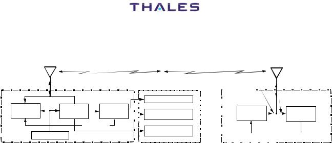
The DME theory of operation is summarized in a block diagram in Figure 1.2.
AIRCRAFT'S |
BEACON'S |
|
ANTENNA |
||
ANTENNA |
||
|
TRANSMITS DISTANCE |
INFORMATION |
and IDENTIFICATION |
SIGNAL |
|
|
|
|
|
|
|
|
|
|
|
|
|
AUTOPILOT |
|
|
|
RECEIVED |
||
|
|
|
|
|
|
|
|
|
|
|
|
|
|
|
|
INTERROGATIONS |
|||
TRANSMITTER |
|
RECEIVER |
|
|
DISTANCE |
|
|
|
|
|
|
|
|
|
|
|
|
|
|
|
|
|
|
|
|
|
|
|
|
|
|
|
|
|
|
||||
|
|
|
|
|
CIRCUITS |
|
|
|
|
|
|
|
DISTANCE INFORMATION |
|
|
|
TRANSMITTER |
|
RECEIVER |
|
|
|
|
|
|
|
|
|
|
|
|
|
TO BOARD INDICATOR |
|
|
|
|
|
|
|
|
|
|
|
|
|
|
|
|
|
|
|
|
||||||
|
|
|
|
|
|
|
|
|
|
|
|
|
|
|
|
|
|
|
|
DME
 AIRBORNE CHANNEL SELECTOR
INTERROGATION |
TRIGGERS |
BEACON |
|
|
REPLY TRIGGER TO |
IDENTIFICATION TONE |
|
|
INTERROGATIONS |
|
|
|
DME GROUND BEACON
Figure 1.2. DME - Theory of operation, simplified block diagram
1.2.1Coverage
According to the frequency band used, the DME system coverage is limited to the optical range and depends on the aircraft flight altitude and on the type of ground.
The high frequency used and the use of special techniques have made the system much less sensitive to site errors than other types of omni-directional beacons now in use.
1.2.2Traffic Capacity
The aircraft handling capacity is adequate for a traffic peak of 200 aircrafts. When the traffic peak exceeds 200 aircrafts the transponder should be capable of handling that peak.
1.2.3Accuracy
As a result of the development and the applications of modern electronic technologies, the accuracy of the distance information provided by the DME system is improving all the time.
At present, the accuracy of a DME system can be considered within the maximum values specified below:
±0.12 NM +0.05% of the distance, from 0 to 65 nautical miles, and ± 0.17 NM +0.05% of the distance, above 65 nautical miles.
1.2.4Nominal Reply Delay – Pair Pulse Code - Channeling
Each beacon is identified by means of its channel frequency, its pulse coding and its identity signal.
The ground beacon introduces a fixed delay between the reception of interrogating pulses and the transmission of the corresponding reply pulses.
This fixed delay, called main delay or fundamental delay, is introduced. So that an aircraft which is flying very close to the beacon can complete transmission of the encoded interrogating pulse pair, and then deactivate its own transmitter, before its receiver begins receiving the corresponding beacon reply pulses.
To render the system as immune as possible to errors caused by interfering signals, the DME system transmits pulse pairs instead of single pulses; each pair includes two 3.5 µs pulses whose spacing depends on the channel mode selected.
The channel code, pulse code, reply delay and operating mode are shown on the following table (standard ICAO).
|
|
Nominal |
Transponder |
Transponder |
|
|
Channel |
Interrogation Pulse Code |
Reply Pulse Code |
Nominal Reply Delay |
|
|
Code |
[µs] |
[µs] |
[µs] |
|
|
X |
12 |
12.0 ± 0.1 |
50 |
|
|
Y |
36 |
30.0 ± 0.1 |
56 |
|
|
|
|
|
|
|
|
|
|
|
|
|
1-2 |
THALES Italia S.p.A.- A. S. D. |
Vers. D, September 2005 |
|
||

DME 415/435 -Technical Manual |
955 900 031C |
|
Vol. 1-Section 1-General Information |
||
|
Each operational channel in the DME system is defined by two frequencies (interrogation and reply frequencies), spaced 63 MHz apart, and by the pulse code for the assigned channel (X or Y channel).
The DME system transmits on a pre-selected channel among the 252 available ones. These channels are divided into 126 X channels and 126 Y channels providing a frequency ranging from 1025 to 1150 MHz for aircraft transmission (interrogation). Moreover, a 962 to 1213 MHz frequency for signal reception by the aircraft (ground beacon reply transmission). Interrogation and reply frequencies are assigned with one MHz spacing between channels.
The diagram shown in figure 1.3 gives the aircraft interrogation frequency associated to the beacon reply frequency for both channel types X, Y. The same information is also given in table 1-1 and table 1-2 for X and Y channels respectively, as per ICAO ANNEX 10.
Each beacon emits a Morse identity code signal that can be heard in the pilot headset; this code consists of pulse pairs transmitted at a frequency of 1350 Hz.
Each beacon is therefore identified by means of its channel frequency, its pulse coding and its identity signal.
|
|
|
Table 1-1. Frequencies for DME Channels |
|
||||
|
|
|
|
|
|
|
|
|
|
|
X Channels (n° 126) |
|
Channel |
Y Channels (n° 126) |
|
||
|
|
I = 1025 + (CH-1) |
|
|
|
I = 1025 + (CH-1) |
|
|
|
|
R = I - 63 |
|
1 ≤ CH ≤ 63 |
R = I + 63 |
|
||
|
|
R = I + 63 |
|
64 ≤ CH ≤ 126 |
R = I - 63 |
|
||
|
I = INTERROGATION FREQUENCY (MHz) |
CH = CHANNEL NUMBER |
|
|||||
|
R = REPLY FREQUENCY (MHz) |
|
|
|
|
|||
960 MHz |
|
|
|
|
|
|
|
1215 MHz |
962 MHz |
|
1025 MHz |
1088 MHz |
1151 MHz |
1213 MHz |
|||
|
|
|
|
|
|
|
|
|
|
|
|
|
|
|
|
|
|
1-63X |
64-126X |
||
|
|
|
|
|
|
|
|
|
|
|
|
|
|
|
|
1-63Y
64-126Y
|
|
|
|
|
|
|
|
|
INTERROGATION FREQUENCIES |
|
REPLY FREQUENCIES |
||
|
|
|
||||
|
|
Figure 1.3. DME Channels Reply and Interrogation Frequencies |
||||
|
|
|
|
|
|
|
Vers. D, September 2005 |
THALES Italia S.p.A.- A. S. D. |
1-3 |
||||

955 900 031C |
DME 415/435 -Technical Manual |
|
Vol. 1-Section 1-General Information |
||
|
Table 1-2. Frequencies and Code Pulses for DME Channels (1 to 17)
|
|
|
|
|
|
|
DME PARAMETERS |
|
|
||
|
|
|
|
|
|
|
|
|
|
|
|
|
CHANNEL PAIRING |
|
|
INTERROGATION |
|
REPLY |
|||||
|
|
|
|
|
|
|
|
|
|
|
|
|
|
|
|
|
|
Pulse Codes |
|
|
|
||
|
|
|
|
|
|
|
|
|
|
|
|
|
|
|
|
|
|
|
DME/P |
|
|
||
|
|
|
|
|
|
|
|
|
|
|
|
|
VHF |
MLS |
|
|
|
|
|
|
|
|
Pulse |
DME |
FREQ. |
FREQ. |
MLS |
Frequency |
DME/N |
|
IAM |
|
FAM |
Frequency |
Codes |
Channel |
MHz |
MHz |
Channel |
MHz |
µs |
|
µs |
|
µs |
MHz |
µs |
1X |
− |
− |
− |
1025 |
12 |
|
− |
|
− |
962 |
12 |
1Y |
− |
− |
− |
1025 |
36 |
|
− |
|
− |
1088 |
30 |
2X |
− |
− |
− |
1026 |
12 |
|
− |
|
− |
963 |
12 |
2Y |
− |
− |
− |
1026 |
36 |
|
− |
|
− |
1089 |
30 |
3X |
− |
− |
− |
1027 |
12 |
|
− |
|
− |
964 |
12 |
3Y |
− |
− |
− |
1027 |
36 |
|
− |
|
− |
1090 |
30 |
4X |
− |
− |
− |
1028 |
12 |
|
− |
|
− |
965 |
12 |
4Y |
− |
− |
− |
1028 |
36 |
|
− |
|
− |
1091 |
30 |
5X |
− |
− |
− |
1029 |
12 |
|
− |
|
− |
966 |
12 |
5Y |
− |
− |
− |
1029 |
36 |
|
− |
|
− |
1092 |
30 |
6X |
− |
− |
− |
1030 |
12 |
|
− |
|
− |
967 |
12 |
6Y |
− |
− |
− |
1030 |
36 |
|
− |
|
− |
1093 |
30 |
7X |
− |
− |
− |
1031 |
12 |
|
− |
|
− |
968 |
12 |
7Y |
− |
− |
− |
1031 |
36 |
|
− |
|
− |
1094 |
30 |
8X |
− |
− |
− |
1032 |
12 |
|
− |
|
− |
969 |
12 |
8Y |
− |
− |
− |
1032 |
36 |
|
− |
|
− |
1095 |
30 |
9X |
− |
− |
− |
1033 |
12 |
|
− |
|
− |
970 |
12 |
9Y |
− |
− |
− |
1033 |
36 |
|
− |
|
− |
1096 |
30 |
10X |
− |
− |
− |
1034 |
12 |
|
− |
|
− |
971 |
12 |
10Y |
− |
− |
− |
1034 |
36 |
|
− |
|
− |
1097 |
30 |
11X |
− |
− |
− |
1035 |
12 |
|
− |
|
− |
972 |
12 |
11Y |
− |
− |
− |
1035 |
36 |
|
− |
|
− |
1098 |
30 |
12X |
− |
− |
− |
1036 |
12 |
|
− |
|
− |
973 |
12 |
12Y |
− |
− |
− |
1036 |
36 |
|
− |
|
− |
1099 |
30 |
13X |
− |
− |
− |
1037 |
12 |
|
− |
|
− |
974 |
12 |
13Y |
− |
− |
− |
1037 |
36 |
|
− |
|
− |
1100 |
30 |
14X |
− |
− |
− |
1038 |
12 |
|
− |
|
− |
975 |
12 |
14Y |
− |
− |
− |
1038 |
36 |
|
− |
|
− |
1101 |
30 |
15X |
− |
− |
− |
1039 |
12 |
|
− |
|
− |
976 |
12 |
15Y |
− |
− |
− |
1039 |
36 |
|
− |
|
− |
1102 |
30 |
16X |
− |
− |
− |
1040 |
12 |
|
− |
|
− |
977 |
12 |
16Y |
− |
− |
− |
1040 |
36 |
|
− |
|
− |
1103 |
30 |
17X |
108.00 |
− |
− |
1041 |
12 |
|
− |
|
− |
978 |
12 |
17Y |
108.05 |
5043.0 |
540 |
1041 |
36 |
|
36 |
|
42 |
1104 |
30 |
17Z |
− |
5043.3 |
541 |
1041 |
− |
|
21 |
|
27 |
1104 |
15 |
|
|
|
|
|
|
|
|
|
|
|
|
1-4 |
THALES Italia S.p.A.- A. S. D. |
Vers. D, September 2005 |

DME 415/435 -Technical Manual |
955 900 031C |
|
Vol. 1-Section 1-General Information |
||
|
Table 1-2. Frequencies and Code Pulses for DME Channels (18 to 28)
|
|
|
|
|
|
|
DME PARAMETERS |
|
|
||
|
|
|
|
|
|
|
|
|
|
|
|
|
CHANNEL PAIRING |
|
|
INTERROGATION |
|
REPLY |
|||||
|
|
|
|
|
|
|
|
|
|
|
|
|
|
|
|
|
|
Pulse Codes |
|
|
|
||
|
|
|
|
|
|
|
DME/P |
|
|
||
|
|
|
|
|
|
|
|
|
|||
|
|
|
|
|
|
|
|
|
|
|
|
|
VHF |
MLS |
|
|
|
|
|
|
|
|
Pulse |
DME |
FREQ. |
FREQ. |
MLS |
Frequency |
DME/N |
|
IAM |
|
FAM |
Frequency |
Codes |
Channel |
MHz |
MHz |
Channel |
MHz |
µs |
|
µs |
|
µs |
MHz |
µs |
18X |
108.10 |
5031.0 |
500 |
1042 |
12 |
|
12 |
|
18 |
979 |
12 |
18W |
− |
5031.3 |
501 |
1042 |
− |
|
24 |
|
30 |
979 |
24 |
18Y |
108.15 |
5043.6 |
542 |
1042 |
36 |
|
36 |
|
42 |
1105 |
30 |
18Z |
− |
5043.9 |
543 |
1042 |
− |
|
21 |
|
27 |
1105 |
15 |
19X |
108.20 |
− |
− |
1043 |
12 |
|
− |
|
− |
980 |
12 |
19Y |
108.25 |
5044.2 |
544 |
1043 |
36 |
|
36 |
|
42 |
1106 |
30 |
19Z |
− |
5044.5 |
545 |
1043 |
− |
|
21 |
|
27 |
1106 |
15 |
20X |
108.30 |
5031.6 |
502 |
1044 |
12 |
|
12 |
|
18 |
981 |
12 |
20W |
− |
5031.9 |
503 |
1044 |
− |
|
24 |
|
30 |
981 |
24 |
20Y |
108.35 |
5044.8 |
546 |
1044 |
36 |
|
36 |
|
42 |
1107 |
30 |
20Z |
− |
5045.1 |
547 |
1044 |
− |
|
21 |
|
27 |
1107 |
15 |
21X |
108.40 |
− |
− |
1045 |
12 |
|
− |
|
− |
982 |
12 |
21Y |
108.45 |
5045.4 |
548 |
1045 |
36 |
|
36 |
|
42 |
1108 |
30 |
21Z |
− |
5045.7 |
549 |
1045 |
− |
|
21 |
|
27 |
1108 |
15 |
22X |
108.50 |
5032.2 |
504 |
1046 |
12 |
|
12 |
|
18 |
983 |
12 |
22W |
− |
5032.5 |
505 |
1046 |
− |
|
24 |
|
30 |
983 |
24 |
22Y |
108.55 |
5046.0 |
550 |
1046 |
36 |
|
36 |
|
42 |
1109 |
30 |
22Z |
− |
5046.3 |
551 |
1046 |
− |
|
21 |
|
27 |
1109 |
15 |
23X |
108.60 |
− |
− |
1047 |
12 |
|
− |
|
− |
984 |
12 |
23Y |
108.65 |
5046.6 |
552 |
1047 |
36 |
|
36 |
|
42 |
1110 |
30 |
23Z |
− |
5046.9 |
553 |
1047 |
− |
|
21 |
|
27 |
1110 |
15 |
24X |
108.70 |
5032.8 |
506 |
1048 |
12 |
|
12 |
|
18 |
985 |
12 |
24W |
− |
5033.1 |
507 |
1048 |
− |
|
24 |
|
30 |
985 |
24 |
24Y |
108.75 |
5047.2 |
554 |
1048 |
36 |
|
36 |
|
42 |
1111 |
30 |
24Z |
− |
5047.5 |
555 |
1048 |
− |
|
21 |
|
27 |
1111 |
15 |
25X |
108.80 |
− |
− |
1049 |
12 |
|
− |
|
− |
986 |
12 |
25Y |
108.85 |
5047.8 |
556 |
1049 |
36 |
|
36 |
|
42 |
1112 |
30 |
25Z |
− |
5048.1 |
557 |
1049 |
− |
|
21 |
|
27 |
1112 |
15 |
26X |
108.90 |
5033.4 |
508 |
1050 |
12 |
|
12 |
|
18 |
987 |
12 |
26W |
− |
5033.7 |
509 |
1050 |
− |
|
24 |
|
30 |
987 |
24 |
26Y |
108.95 |
5048.4 |
558 |
1050 |
36 |
|
36 |
|
42 |
1113 |
30 |
26Z |
− |
5048.7 |
559 |
1050 |
− |
|
21 |
|
27 |
1113 |
15 |
27X |
109.00 |
− |
− |
1051 |
12 |
|
− |
|
− |
988 |
12 |
27Y |
109.05 |
5049.0 |
560 |
1051 |
36 |
|
36 |
|
42 |
1114 |
30 |
27Z |
− |
5049.3 |
561 |
1051 |
− |
|
21 |
|
27 |
1114 |
15 |
28X |
109.10 |
5034.0 |
510 |
1052 |
12 |
|
12 |
|
18 |
989 |
12 |
28W |
− |
5034.3 |
511 |
1052 |
− |
|
24 |
|
30 |
989 |
24 |
28Y |
109.15 |
5049.6 |
562 |
1052 |
36 |
|
36 |
|
42 |
1115 |
30 |
28Z |
− |
5049.9 |
563 |
1052 |
− |
|
21 |
|
27 |
1115 |
15 |
|
|
|
|
|
|
|
|
|
|
|
|
Vers. D, September 2005 |
THALES Italia S.p.A.- A. S. D. |
1-5 |

955 900 031C |
DME 415/435 -Technical Manual |
|
Vol. 1-Section 1-General Information |
||
|
Table 1-2. Frequencies and Code Pulses for DME Channels (29 to 40)
|
|
|
|
|
|
|
DME PARAMETERS |
|
|
||
|
|
|
|
|
|
|
|
|
|
|
|
|
CHANNEL PAIRING |
|
|
INTERROGATION |
|
REPLY |
|||||
|
|
|
|
|
|
|
|
|
|
|
|
|
|
|
|
|
|
Pulse Codes |
|
|
|
||
|
|
|
|
|
|
|
|
|
|
|
|
|
|
|
|
|
|
|
DME/P |
|
|
||
|
|
|
|
|
|
|
|
|
|
|
|
|
VHF |
MLS |
|
|
|
|
|
|
|
|
Pulse |
DME |
FREQ. |
FREQ. |
MLS |
Frequency |
DME/N |
|
IAM |
|
FAM |
Frequency |
Codes |
Channel |
MHz |
MHz |
Channel |
MHz |
µs |
|
µs |
|
µs |
MHz |
µs |
29X |
109.20 |
− |
− |
1053 |
12 |
|
− |
|
− |
990 |
12 |
29Y |
109.25 |
5050.2 |
564 |
1053 |
36 |
|
36 |
|
42 |
1116 |
30 |
29Z |
− |
5050.5 |
565 |
1053 |
− |
|
21 |
|
27 |
1116 |
15 |
30X |
109.30 |
5034.6 |
512 |
1054 |
12 |
|
12 |
|
18 |
991 |
12 |
30W |
− |
5034.9 |
513 |
1054 |
− |
|
24 |
|
30 |
991 |
24 |
30Y |
109.35 |
5050.8 |
566 |
1054 |
36 |
|
36 |
|
42 |
1117 |
30 |
30Z |
− |
5051.1 |
567 |
1054 |
− |
|
21 |
|
27 |
1117 |
15 |
31X |
109.40 |
− |
− |
1055 |
12 |
|
− |
|
− |
992 |
12 |
31Y |
109.45 |
5051.4 |
568 |
1055 |
36 |
|
36 |
|
42 |
1118 |
30 |
31Z |
− |
5051.7 |
569 |
1055 |
− |
|
21 |
|
27 |
1118 |
15 |
32X |
109.50 |
5035.2 |
514 |
1056 |
12 |
|
12 |
|
18 |
993 |
12 |
32W |
− |
5035.5 |
515 |
1056 |
− |
|
24 |
|
30 |
993 |
24 |
32Y |
109.55 |
5052.0 |
570 |
1056 |
36 |
|
36 |
|
42 |
1119 |
30 |
32Z |
− |
5052.3 |
571 |
1056 |
− |
|
21 |
|
27 |
1119 |
15 |
33X |
109.60 |
− |
− |
1057 |
12 |
|
− |
|
− |
994 |
12 |
33Y |
109.65 |
5052.6 |
572 |
1057 |
36 |
|
36 |
|
42 |
1120 |
30 |
33Z |
− |
5052.9 |
573 |
1057 |
− |
|
21 |
|
27 |
1120 |
15 |
34X |
109.70 |
5035.8 |
516 |
1058 |
12 |
|
12 |
|
18 |
995 |
12 |
34W |
− |
5036.1 |
517 |
1058 |
− |
|
24 |
|
30 |
995 |
24 |
34Y |
109.75 |
5053.2 |
574 |
1058 |
36 |
|
36 |
|
42 |
1121 |
30 |
34Z |
− |
5053.5 |
575 |
1058 |
− |
|
21 |
|
27 |
1121 |
15 |
35X |
109.80 |
− |
− |
1059 |
12 |
|
− |
|
− |
996 |
12 |
35Y |
109.85 |
5053.8 |
576 |
1059 |
36 |
|
36 |
|
42 |
1122 |
30 |
35Z |
− |
5054.1 |
577 |
1059 |
− |
|
21 |
|
27 |
1122 |
15 |
36X |
109.90 |
5036.4 |
518 |
1060 |
12 |
|
12 |
|
18 |
997 |
12 |
36W |
− |
5036.7 |
519 |
1060 |
− |
|
24 |
|
30 |
997 |
24 |
36Y |
109.95 |
5054.4 |
578 |
1060 |
36 |
|
36 |
|
42 |
1123 |
30 |
36Z |
− |
5054.7 |
579 |
1060 |
− |
|
21 |
|
27 |
1123 |
15 |
37X |
110.00 |
− |
− |
1061 |
12 |
|
− |
|
− |
998 |
12 |
37Y |
110.05 |
5055.0 |
580 |
1061 |
36 |
|
36 |
|
42 |
1124 |
30 |
37Z |
− |
5055.3 |
581 |
1061 |
− |
|
21 |
|
27 |
1124 |
15 |
38X |
110.10 |
5037.0 |
520 |
1062 |
12 |
|
12 |
|
18 |
999 |
12 |
38W |
− |
5037.3 |
521 |
1062 |
− |
|
24 |
|
30 |
999 |
24 |
38Y |
110.15 |
5055.6 |
582 |
1062 |
36 |
|
36 |
|
42 |
1125 |
30 |
38Z |
− |
5055.9 |
583 |
1062 |
− |
|
21 |
|
27 |
1125 |
15 |
39X |
110.20 |
− |
− |
1063 |
12 |
|
− |
|
− |
1000 |
12 |
39Y |
110.25 |
5056.2 |
584 |
1063 |
36 |
|
36 |
|
42 |
1126 |
30 |
39Z |
− |
5056.5 |
585 |
1063 |
− |
|
21 |
|
27 |
1126 |
15 |
40X |
110.30 |
5037.6 |
522 |
1064 |
12 |
|
12 |
|
18 |
1001 |
12 |
40W |
− |
5037.9 |
523 |
1064 |
− |
|
24 |
|
30 |
1001 |
24 |
40Y |
110.35 |
5056.8 |
586 |
1064 |
36 |
|
36 |
|
42 |
1127 |
30 |
40Z |
− |
5057.1 |
587 |
1064 |
− |
|
21 |
|
27 |
1127 |
15 |
|
|
|
|
|
|
|
|
|
|
|
|
1-6 |
THALES Italia S.p.A.- A. S. D. |
Vers. D, September 2005 |

DME 415/435 -Technical Manual |
955 900 031C |
|
Vol. 1-Section 1-General Information |
||
|
Table 1-2. Frequencies and Code Pulses for DME Channels (41 to 52)
|
|
|
|
|
|
|
DME PARAMETERS |
|
|
||
|
|
|
|
|
|
|
|
|
|
|
|
|
CHANNEL PAIRING |
|
|
INTERROGATION |
|
REPLY |
|||||
|
|
|
|
|
|
|
|
|
|
|
|
|
|
|
|
|
|
Pulse Codes |
|
|
|
||
|
|
|
|
|
|
|
DME/P |
|
|
||
|
|
|
|
|
|
|
|
|
|||
|
|
|
|
|
|
|
|
|
|
|
|
|
VHF |
MLS |
|
|
|
|
|
|
|
|
Pulse |
DME |
FREQ. |
FREQ. |
MLS |
Frequency |
DME/N |
|
IAM |
|
FAM |
Frequency |
Codes |
Channel |
MHz |
MHz |
Channel |
MHz |
µs |
|
µs |
|
µs |
MHz |
µs |
41X |
110.40 |
− |
− |
1065 |
12 |
|
− |
|
− |
1002 |
12 |
41Y |
110.45 |
5057.4 |
588 |
1065 |
36 |
|
36 |
|
42 |
1128 |
30 |
41Z |
− |
5057.7 |
589 |
1065 |
− |
|
21 |
|
27 |
1128 |
15 |
42X |
110.50 |
5038.2 |
524 |
1066 |
12 |
|
12 |
|
18 |
1003 |
12 |
42W |
− |
5038.5 |
525 |
1066 |
− |
|
24 |
|
30 |
1003 |
24 |
42Y |
110.55 |
5058.0 |
590 |
1066 |
36 |
|
36 |
|
42 |
1129 |
30 |
42Z |
− |
5058.3 |
591 |
1066 |
− |
|
21 |
|
27 |
1129 |
15 |
43X |
110.60 |
− |
− |
1067 |
12 |
|
− |
|
− |
1004 |
12 |
43Y |
110.65 |
5058.6 |
592 |
1067 |
36 |
|
36 |
|
42 |
1130 |
30 |
43Z |
− |
5058.9 |
593 |
1067 |
− |
|
21 |
|
27 |
1130 |
15 |
44X |
110.70 |
5038.8 |
526 |
1068 |
12 |
|
12 |
|
18 |
1005 |
12 |
44W |
− |
5039.1 |
527 |
1068 |
− |
|
24 |
|
30 |
1005 |
24 |
44Y |
110.75 |
5059.2 |
594 |
1068 |
36 |
|
36 |
|
42 |
1131 |
30 |
44Z |
− |
5059.5 |
595 |
1068 |
− |
|
21 |
|
27 |
1131 |
15 |
45X |
110.80 |
− |
− |
1069 |
12 |
|
− |
|
− |
1006 |
12 |
45Y |
110.85 |
5059.8 |
596 |
1069 |
36 |
|
36 |
|
42 |
1132 |
30 |
45Z |
− |
5060.1 |
597 |
1069 |
− |
|
21 |
|
27 |
1132 |
15 |
46X |
110.90 |
5039.4 |
528 |
1070 |
12 |
|
12 |
|
18 |
1007 |
12 |
46W |
− |
5039.7 |
529 |
1070 |
− |
|
24 |
|
30 |
1007 |
24 |
46Y |
110.95 |
5060.4 |
598 |
1070 |
36 |
|
36 |
|
42 |
1133 |
30 |
46Z |
− |
5060.7 |
599 |
1070 |
− |
|
21 |
|
27 |
1133 |
15 |
47X |
111.00 |
− |
− |
1071 |
12 |
|
− |
|
− |
1008 |
12 |
47Y |
111.05 |
5061.0 |
600 |
1071 |
36 |
|
36 |
|
42 |
1134 |
30 |
47Z |
− |
5061.3 |
601 |
1071 |
− |
|
21 |
|
27 |
1134 |
15 |
48X |
111.10 |
5040.0 |
530 |
1072 |
12 |
|
12 |
|
18 |
1009 |
12 |
48W |
− |
5040.3 |
531 |
1072 |
− |
|
24 |
|
30 |
1009 |
24 |
48Y |
111.15 |
5061.6 |
602 |
1072 |
36 |
|
36 |
|
42 |
1135 |
30 |
48Z |
− |
5061.9 |
603 |
1072 |
− |
|
21 |
|
27 |
1135 |
15 |
49X |
111.20 |
− |
− |
1073 |
12 |
|
− |
|
− |
1010 |
12 |
49Y |
111.25 |
5062.2 |
604 |
1073 |
36 |
|
36 |
|
42 |
1136 |
30 |
49Z |
− |
5062.5 |
605 |
1073 |
− |
|
21 |
|
27 |
1136 |
15 |
50X |
111.30 |
5040.6 |
532 |
1074 |
12 |
|
12 |
|
18 |
1011 |
12 |
50W |
− |
5040.9 |
533 |
1074 |
− |
|
24 |
|
30 |
1011 |
24 |
50Y |
111.35 |
5062.8 |
606 |
1074 |
36 |
|
36 |
|
42 |
1137 |
30 |
50Z |
− |
5063.1 |
607 |
1074 |
− |
|
21 |
|
27 |
1137 |
15 |
51X |
111.40 |
− |
− |
1075 |
12 |
|
− |
|
− |
1012 |
12 |
51Y |
111.45 |
5063.4 |
608 |
1075 |
36 |
|
36 |
|
42 |
1138 |
30 |
51Z |
− |
5063.7 |
609 |
1075 |
− |
|
21 |
|
27 |
1138 |
15 |
52X |
111.50 |
5041.2 |
534 |
1076 |
12 |
|
12 |
|
18 |
1013 |
12 |
52W |
− |
5041.5 |
535 |
1076 |
− |
|
24 |
|
30 |
1013 |
24 |
52Y |
111.55 |
5064.0 |
610 |
1076 |
36 |
|
36 |
|
42 |
1139 |
30 |
52Z |
− |
5064.3 |
611 |
1076 |
− |
|
21 |
|
27 |
1139 |
15 |
|
|
|
|
|
|
|
|
|
|
|
|
Vers. D, September 2005 |
THALES Italia S.p.A.- A. S. D. |
1-7 |

955 900 031C |
DME 415/435 -Technical Manual |
|
Vol. 1-Section 1-General Information |
||
|
Table 1-2. Frequencies and Code Pulses for DME Channels (53 to 68)
|
|
|
|
|
|
|
DME PARAMETERS |
|
|
||
|
|
|
|
|
|
|
|
|
|
|
|
|
CHANNEL PAIRING |
|
|
INTERROGATION |
|
REPLY |
|||||
|
|
|
|
|
|
|
|
|
|
|
|
|
|
|
|
|
|
Pulse Codes |
|
|
|
||
|
|
|
|
|
|
|
|
|
|
|
|
|
|
|
|
|
|
|
DME/P |
|
|
||
|
|
|
|
|
|
|
|
|
|
|
|
|
VHF |
MLS |
|
|
|
|
|
|
|
|
Pulse |
DME |
FREQ. |
FREQ. |
MLS |
Frequency |
DME/N |
|
IAM |
|
FAM |
Frequency |
Codes |
Channel |
MHz |
MHz |
Channel |
MHz |
µs |
|
µs |
|
µs |
MHz |
µs |
53X |
111.60 |
− |
− |
1077 |
12 |
|
− |
|
− |
1014 |
12 |
53Y |
111.65 |
5064.5 |
612 |
1077 |
36 |
|
36 |
|
42 |
1140 |
30 |
53Z |
− |
5064.9 |
613 |
1077 |
− |
|
21 |
|
27 |
1140 |
15 |
54X |
111.70 |
5041.8 |
536 |
1078 |
12 |
|
12 |
|
18 |
1015 |
12 |
54W |
− |
5042.1 |
537 |
1078 |
− |
|
24 |
|
30 |
1015 |
24 |
54Y |
111.75 |
5065.2 |
614 |
1078 |
36 |
|
36 |
|
42 |
1141 |
30 |
54Z |
− |
5065.5 |
615 |
1078 |
− |
|
21 |
|
27 |
1141 |
15 |
55X |
111.80 |
− |
− |
1079 |
12 |
|
− |
|
− |
1016 |
12 |
55Y |
111.85 |
5065.8 |
616 |
1079 |
36 |
|
36 |
|
42 |
1142 |
30 |
55Z |
− |
5066.1 |
617 |
1079 |
− |
|
21 |
|
27 |
1142 |
15 |
56X |
111.90 |
5042.4 |
538 |
1080 |
12 |
|
12 |
|
18 |
1017 |
12 |
56W |
− |
5042.7 |
539 |
1080 |
− |
|
24 |
|
30 |
1017 |
24 |
56Y |
111.95 |
5066.4 |
618 |
1080 |
36 |
|
36 |
|
42 |
1143 |
30 |
56Z |
− |
5066.7 |
619 |
1080 |
− |
|
21 |
|
27 |
1143 |
15 |
57X |
112.00 |
− |
− |
1081 |
12 |
|
− |
|
− |
1018 |
12 |
57Y |
112.05 |
− |
− |
1081 |
36 |
|
− |
|
− |
1144 |
30 |
58X |
112.10 |
− |
− |
1082 |
12 |
|
− |
|
− |
1019 |
12 |
58Y |
112.15 |
− |
− |
1082 |
36 |
|
− |
|
− |
1145 |
30 |
59X |
112.20 |
− |
− |
1083 |
12 |
|
− |
|
− |
1020 |
12 |
59Y |
112.25 |
− |
− |
1083 |
36 |
|
− |
|
− |
1146 |
30 |
60X |
− |
− |
− |
1084 |
12 |
|
− |
|
− |
1021 |
12 |
60Y |
− |
− |
− |
1084 |
36 |
|
− |
|
− |
1147 |
30 |
61X |
− |
− |
− |
1085 |
12 |
|
− |
|
− |
1022 |
12 |
61Y |
− |
− |
− |
1085 |
36 |
|
− |
|
− |
1148 |
30 |
62X |
− |
− |
− |
1086 |
12 |
|
− |
|
− |
1023 |
12 |
62Y |
− |
− |
− |
1086 |
36 |
|
− |
|
− |
1149 |
30 |
63X |
− |
− |
− |
1087 |
12 |
|
− |
|
− |
1024 |
12 |
63Y |
− |
− |
− |
1087 |
36 |
|
− |
|
− |
1150 |
30 |
64X |
− |
− |
− |
1088 |
12 |
|
− |
|
− |
1151 |
12 |
64Y |
− |
− |
− |
1088 |
36 |
|
− |
|
− |
1025 |
30 |
65X |
− |
− |
− |
1089 |
12 |
|
− |
|
− |
1152 |
12 |
65Y |
− |
− |
− |
1089 |
36 |
|
− |
|
− |
1026 |
30 |
66X |
− |
− |
− |
1090 |
12 |
|
− |
|
− |
1153 |
12 |
66Y |
− |
− |
− |
1090 |
36 |
|
− |
|
− |
1027 |
30 |
67X |
− |
− |
− |
1091 |
12 |
|
− |
|
− |
1154 |
12 |
67Y |
− |
− |
− |
1091 |
36 |
|
− |
|
− |
1028 |
30 |
68X |
− |
− |
− |
1092 |
12 |
|
− |
|
− |
1155 |
12 |
68Y |
− |
− |
− |
1092 |
36 |
|
− |
|
− |
1029 |
30 |
|
|
|
|
|
|
|
|
|
|
|
|
1-8 |
THALES Italia S.p.A.- A. S. D. |
Vers. D, September 2005 |

DME 415/435 -Technical Manual |
955 900 031C |
|
Vol. 1-Section 1-General Information |
||
|
Table 1-2. Frequencies and Code Pulses for DME Channels (69 to 85)
|
|
|
|
|
|
|
DME PARAMETERS |
|
|
||
|
|
|
|
|
|
|
|
|
|
|
|
|
CHANNEL PAIRING |
|
|
INTERROGATION |
|
REPLY |
|||||
|
|
|
|
|
|
|
|
|
|
|
|
|
|
|
|
|
|
Pulse Codes |
|
|
|
||
|
|
|
|
|
|
|
DME/P |
|
|
||
|
|
|
|
|
|
|
|
|
|||
|
|
|
|
|
|
|
|
|
|
|
|
|
VHF |
MLS |
|
|
|
|
|
|
|
|
Pulse |
DME |
FREQ. |
FREQ. |
MLS |
Frequency |
DME/N |
|
IAM |
|
FAM |
Frequency |
Codes |
Channel |
MHz |
MHz |
Channel |
MHz |
µs |
|
µs |
|
µs |
MHz |
µs |
69X |
− |
− |
− |
1093 |
12 |
|
− |
|
− |
1156 |
12 |
69Y |
− |
− |
− |
1093 |
36 |
|
− |
|
− |
1030 |
30 |
70X |
112.30 |
− |
− |
1094 |
12 |
|
− |
|
− |
1157 |
12 |
70Y |
112.35 |
− |
− |
1094 |
36 |
|
− |
|
− |
1031 |
30 |
71X |
112.40 |
− |
− |
1095 |
12 |
|
− |
|
− |
1158 |
12 |
71Y |
112.45 |
− |
− |
1095 |
36 |
|
− |
|
− |
1032 |
30 |
72X |
112.50 |
− |
− |
1096 |
12 |
|
− |
|
− |
1159 |
12 |
72Y |
112.55 |
− |
− |
1096 |
36 |
|
− |
|
− |
1033 |
30 |
73X |
112.60 |
− |
− |
1097 |
12 |
|
− |
|
− |
1160 |
12 |
73Y |
112.65 |
− |
− |
1097 |
36 |
|
− |
|
− |
1034 |
30 |
74X |
112.70 |
− |
− |
1098 |
12 |
|
− |
|
− |
1161 |
12 |
74Y |
112.75 |
− |
− |
1098 |
36 |
|
− |
|
− |
1035 |
30 |
75X |
112.80 |
− |
− |
1099 |
12 |
|
− |
|
− |
1162 |
12 |
75Y |
112.85 |
− |
− |
1099 |
36 |
|
− |
|
− |
1036 |
30 |
76X |
112.90 |
− |
− |
1100 |
12 |
|
− |
|
− |
1163 |
12 |
76Y |
112.95 |
− |
− |
1100 |
36 |
|
− |
|
− |
1037 |
30 |
77X |
113.00 |
− |
− |
1101 |
12 |
|
− |
|
− |
1164 |
12 |
77Y |
113.05 |
− |
− |
1101 |
36 |
|
− |
|
− |
1038 |
30 |
78Y |
113.10 |
− |
− |
1102 |
12 |
|
− |
|
− |
1165 |
12 |
78Y |
113.15 |
− |
− |
1102 |
36 |
|
− |
|
− |
1039 |
30 |
79X |
113.20 |
− |
− |
1103 |
12 |
|
− |
|
− |
1166 |
12 |
79Y |
113.25 |
− |
− |
1103 |
36 |
|
− |
|
− |
1040 |
30 |
80X |
113.30 |
− |
− |
1104 |
12 |
|
− |
|
− |
1167 |
12 |
80Y |
113.35 |
5067.0 |
620 |
1104 |
36 |
|
36 |
|
42 |
1041 |
30 |
80Z |
− |
5067.3 |
621 |
1104 |
− |
|
21 |
|
27 |
1041 |
15 |
81X |
113.40 |
− |
− |
1105 |
12 |
|
− |
|
− |
1168 |
12 |
81Y |
113.45 |
5067.6 |
622 |
1105 |
36 |
|
36 |
|
42 |
1042 |
30 |
81Z |
− |
5067.9 |
623 |
1105 |
− |
|
21 |
|
27 |
1042 |
15 |
82X |
113.50 |
− |
− |
1106 |
12 |
|
− |
|
− |
1169 |
12 |
82Y |
113.55 |
5068.2 |
624 |
1106 |
36 |
|
36 |
|
42 |
1043 |
30 |
82Z |
− |
5068.5 |
625 |
1106 |
− |
|
21 |
|
27 |
1043 |
15 |
83X |
113.60 |
− |
− |
1107 |
12 |
|
− |
|
− |
1170 |
12 |
83Y |
113.65 |
5068.8 |
626 |
1107 |
36 |
|
36 |
|
42 |
1044 |
30 |
83Z |
− |
5069.1 |
627 |
1107 |
− |
|
21 |
|
27 |
1044 |
15 |
84X |
113.70 |
− |
− |
1108 |
12 |
|
− |
|
− |
1171 |
12 |
84Y |
113.75 |
5069.4 |
628 |
1108 |
36 |
|
36 |
|
42 |
1045 |
30 |
84Z |
− |
5069.7 |
629 |
1108 |
− |
|
21 |
|
27 |
1045 |
15 |
85X |
113,80 |
|
|
1109 |
12 |
|
- |
|
- |
1172 |
12 |
85Y |
113,85 |
5070.0 |
|
1109 |
36 |
|
36 |
|
42 |
1046 |
30 |
85Z |
- |
5071.3 |
|
1109 |
- |
|
21 |
|
27 |
1046 |
15 |
|
|
|
|
|
|
|
|
|
|
|
|
Vers. D, September 2005 |
THALES Italia S.p.A.- A. S. D. |
1-9 |

955 900 031C |
DME 415/435 -Technical Manual |
|
Vol. 1-Section 1-General Information |
||
|
Table 1-2. Frequencies and Code Pulses for DME Channels (86 to 99)
|
|
|
|
|
|
|
DME PARAMETERS |
|
|
||
|
|
|
|
|
|
|
|
|
|
|
|
|
CHANNEL PAIRING |
|
|
INTERROGATION |
|
REPLY |
|||||
|
|
|
|
|
|
|
|
|
|
|
|
|
|
|
|
|
|
Pulse Codes |
|
|
|
||
|
|
|
|
|
|
|
|
|
|
|
|
|
|
|
|
|
|
|
DME/P |
|
|
||
|
|
|
|
|
|
|
|
|
|
|
|
|
VHF |
MLS |
|
|
|
|
|
|
|
|
Pulse |
DME |
FREQ. |
FREQ. |
MLS |
Frequency |
DME/N |
|
IAM |
|
FAM |
Frequency |
Codes |
Channel |
MHz |
MHz |
Channel |
MHz |
µs |
|
µs |
|
µs |
MHz |
µs |
86X |
113.90 |
− |
− |
1110 |
12 |
|
− |
|
− |
1173 |
12 |
86Y |
113.95 |
5070.6 |
632 |
1110 |
36 |
|
36 |
|
42 |
1047 |
30 |
86Z |
− |
5070.9 |
633 |
1110 |
− |
|
21 |
|
27 |
1047 |
15 |
87X |
114.00 |
− |
− |
1111 |
12 |
|
− |
|
− |
1174 |
12 |
87Y |
114.05 |
5071.2 |
634 |
1111 |
36 |
|
36 |
|
42 |
1048 |
30 |
87Z |
− |
5071.5 |
635 |
1111 |
− |
|
21 |
|
27 |
1048 |
15 |
88X |
114.10 |
− |
− |
1112 |
12 |
|
− |
|
− |
1175 |
12 |
88Y |
114.15 |
5071.8 |
636 |
1112 |
36 |
|
36 |
|
42 |
1049 |
30 |
88Z |
− |
5072.1 |
637 |
1112 |
− |
|
21 |
|
27 |
1049 |
15 |
89X |
114.20 |
− |
− |
1113 |
12 |
|
− |
|
− |
1176 |
12 |
89Y |
114.25 |
5072.4 |
638 |
1113 |
36 |
|
36 |
|
42 |
1050 |
30 |
89Z |
− |
5072.7 |
639 |
1113 |
− |
|
21 |
|
27 |
1050 |
15 |
90X |
114.30 |
− |
− |
1114 |
12 |
|
− |
|
− |
1177 |
12 |
90Y |
114.35 |
5073.0 |
640 |
1114 |
36 |
|
36 |
|
42 |
1051 |
30 |
90Z |
− |
5073.3 |
641 |
1114 |
− |
|
21 |
|
27 |
1051 |
15 |
91X |
114.40 |
− |
− |
1115 |
12 |
|
− |
|
− |
1178 |
12 |
91Y |
114.45 |
5073.6 |
642 |
1115 |
36 |
|
36 |
|
42 |
1052 |
30 |
91Z |
− |
5073.9 |
643 |
1115 |
− |
|
21 |
|
27 |
1052 |
15 |
92X |
114.50 |
− |
− |
1116 |
12 |
|
− |
|
− |
1179 |
12 |
92Y |
114.55 |
5074.2 |
644 |
1116 |
36 |
|
36 |
|
42 |
1053 |
30 |
92Z |
− |
5074.5 |
645 |
1116 |
− |
|
21 |
|
27 |
1053 |
15 |
93X |
114.60 |
− |
− |
1117 |
12 |
|
− |
|
− |
1180 |
12 |
93Y |
114.65 |
5074.8 |
646 |
1117 |
36 |
|
36 |
|
42 |
1054 |
30 |
93Z |
− |
5075.1 |
647 |
1117 |
− |
|
21 |
|
27 |
1054 |
15 |
94X |
114.70 |
− |
− |
1118 |
12 |
|
− |
|
− |
1181 |
12 |
94Y |
114.75 |
5075.4 |
648 |
1118 |
36 |
|
36 |
|
42 |
1055 |
30 |
94Z |
− |
5075.7 |
649 |
1118 |
− |
|
21 |
|
27 |
1055 |
15 |
95X |
114.80 |
− |
− |
1119 |
12 |
|
− |
|
− |
1182 |
12 |
95Y |
114.85 |
5076.0 |
650 |
1119 |
36 |
|
36 |
|
42 |
1056 |
30 |
95Z |
− |
5076.3 |
651 |
1119 |
− |
|
21 |
|
27 |
1056 |
15 |
96X |
114.90 |
− |
− |
1120 |
12 |
|
− |
|
− |
1183 |
12 |
96Y |
114.95 |
5076.6 |
652 |
1120 |
36 |
|
36 |
|
42 |
1057 |
30 |
96Z |
− |
5076.9 |
653 |
1120 |
− |
|
21 |
|
27 |
1057 |
15 |
97X |
115.00 |
− |
− |
1121 |
12 |
|
− |
|
− |
1184 |
12 |
97Y |
115.05 |
5077.2 |
654 |
1121 |
36 |
|
36 |
|
42 |
1058 |
30 |
97Z |
− |
5077.5 |
655 |
1121 |
− |
|
21 |
|
27 |
1058 |
15 |
98X |
115.10 |
− |
− |
1122 |
12 |
|
− |
|
− |
1185 |
12 |
98Y |
115.15 |
5077.8 |
656 |
1122 |
36 |
|
36 |
|
42 |
1059 |
30 |
98Z |
− |
5078.1 |
657 |
1122 |
− |
|
21 |
|
27 |
1059 |
15 |
99X |
115.20 |
− |
− |
1123 |
12 |
|
− |
|
− |
1186 |
12 |
99Y |
115.25 |
5078.4 |
658 |
1123 |
36 |
|
36 |
|
42 |
1060 |
30 |
99Z |
− |
5078.7 |
659 |
1123 |
− |
|
21 |
|
27 |
1060 |
15 |
|
|
|
|
|
|
|
|
|
|
|
|
1-10 |
THALES Italia S.p.A.- A. S. D. |
Vers. D, September 2005 |
 Loading...