

Thales ATM 435 Users Manual

Description, Installation, Operation, Maintenance Reference: Vol. 1 Code 955 900 031C
GROUND BEACON
DME 415/435
Technical Manual
VOLUME 1
Equipment description, Installation, Operation, Maintenance and PC user
SECTION 1
GENERAL INFORMATION
Vers. D, September 2005
THALES Italia S.p.A.- Air Systems Division

955 900 031C
DME 415/435 -Technical Manual
Vol. 1-Section 1-General Information
1-II
THALES Italia S.p.A.- A. S. D.
Vers. D, September 2005

DME 415/435 -Technical Manual
Vol. 1-Section 1-General Information
955 900 031C
Table of CONTENTS
Paragraph Page
SECTION 1............................................................................................................................................1-1
GENERAL INFORMATION....................................................................................................1-1
1.1 INTRODUCTION ..............................................................................................................1-1
1.2 DME PRINCIPLE ..............................................................................................................1-1
1.2.1 Coverage ..........................................................................................................................1-2
1.2.2 Traffic Capacity .................................................................................................................1-2
1.2.3 Accuracy ...........................................................................................................................1-2
1.2.4 Nominal Reply Delay – Pair Pulse Code - Channeling.....................................................1-2
1.3 GENERAL FEATURES OF THE EQUIPMENT................................................................1-13
1.3.1 Equipment Versions..........................................................................................................1-13
1.3.2 Main Feature of the Equipment ........................................................................................1-13
1.3.2.1 Engineering.......................................................................................................................1-14
1.3.2.2 Safety................................................................................................................................1-14
1.3.2.3 Installation.........................................................................................................................1-14
1.3.2.4 Operation ..........................................................................................................................1-14
1.4 BEACON COMPOSITION AND IDENTIFICATION..........................................................1-16
1.5 PHYSICAL AND MECHANICAL general Description.......................................................1-19
1.6 EQUIPMENT FUNCTIONAL DESCRIPTION...................................................................1-26
1.6.1 General Overview .............................................................................................................1-26
1.6.2 DME 415/435 System Functional Description ..................................................................1-27
1.6.3 I/O SYSTEM - Functional description ...............................................................................1-31
1.6.3.1 I/O Local site .....................................................................................................................1-31
1.6.3.2 LOCAL CONTROL & STATUS UNIT (LCSU) ..................................................................1-34
1.6.3.2.1 CONTROL AND STATUS BOARD - CSB module – Functional description....................1-36
1.6.3.2.1.1 CPU and Memories...........................................................................................................1-37
1.6.3.2.1.2 Serial Lines .......................................................................................................................1-40
1.6.3.2.1.3 Parallel ports .....................................................................................................................1-41
1.6.3.2.2 LOCAL FRONT CONTROL PANEL .................................................................................1-44
1.6.3.2.2.1 INDICATION AND CONTROLS - INC Module - functional description............................1-45
1.6.3.3 REMOTE CONTROL SYSTEM ........................................................................................1-48
1.6.3.3.1 Remote Control & Status Indicator (RCSI 446) ................................................................1-50
1.6.3.3.2 Remote Control and Status Equipment (RCSE)...............................................................1-51
1.6.3.3.3 MCS ..................................................................................................................................1-52
1.6.3.4 Status Indicator SI 446......................................................................................................1-53
1.6.3.5 Personal Computer - PC...................................................................................................1-54
1.6.4 TRANSPONDER – Functional description .......................................................................1-55
1.6.4.1 General Overviews ...........................................................................................................1-55
1.6.4.1.1 Pilot Pulse .........................................................................................................................1-55
1.6.4.1.2 Transponder Main Delay Measurement ...........................................................................1-55
1.6.4.2 RECEIVER - RX module...................................................................................................1-60
1.6.4.2.1 UHF coupler (pilot pulse mixer) and 63 MHz Oscillator....................................................1-61
1.6.4.2.2 UHF Front End & 63 MHz linear amplification..................................................................1-61
1.6.4.2.3 Synthesizer .......................................................................................................................1-62
1.6.4.2.4 Programmable attenuators ...............................................................................................1-62
1.6.4.2.5 Logarithmic Amplifier ........................................................................................................1-63
1.6.4.2.6 On channel validation (OCV) ............................................................................................1-63
1.6.4.2.7 RX reference power supply ..............................................................................................1-63
1.6.4.2.8 Digital circuitry and data bus,............................................................................................1-64
Vers. D, September 2005
THALES Italia S.p.A.- A. S. D.
1-a

955 900 031C
Paragraph Page
DME 415/435 -Technical Manual
Vol. 1-Section 1-General Information
1.6.4.3 SIGNAL PROCESSOR - DPR module ............................................................................1-66
1.6.4.3.1 Analog Input, TOA & Delay Compare ............................................................................. 1-68
1.6.4.3.2 On-channel validate .........................................................................................................1-69
1.6.4.3.3 Decoder and Dead Time .................................................................................................. 1-69
1.6.4.3.4 Echo suppression............................................................................................................. 1-70
1.6.4.3.5 Main Delay & Priority Circuit............................................................................................. 1-71
1.6.4.3.6 Keyer and 1350 Hz Generator .........................................................................................1-71
1.6.4.3.7 Squitter Generator........................................................................................................... 1-72
1.6.4.3.8 DPR reference power supply ...........................................................................................1-72
1.6.4.3.9 Digital Input circuitry and Data bus .................................................................................. 1-72
1.6.4.4 MODULATOR – DMD module .........................................................................................1-73
1.6.4.4.1 Microprocessor and Peripherals ...................................................................................... 1-75
1.6.4.4.1.1 Watchdog and Power-On Reset ...................................................................................... 1-75
1.6.4.4.1.2 Serial Communication Controller ..................................................................................... 1-75
1.6.4.4.1.3 Internal Timers .................................................................................................................1-75
1.6.4.4.2 Coded Gaussian former & Pedestal Modulation Generators........................................... 1-75
1.6.4.4.3 Coded Square Gates Modulation..................................................................................... 1-76
1.6.4.4.4 Scan & Calibration Counters and reply delay Fine compensation.................................. 1-76
1.6.4.4.4.1 Overload Protection.......................................................................................................... 1-77
1.6.4.4.5 Acquisition Process .......................................................................................................... 1-77
1.6.4.4.6 Modulation signals measurements................................................................................... 1-77
1.6.4.4.7 DMD reference power supply........................................................................................... 1-77
1.6.4.4.8 Digital Input and Data bus ................................................................................................ 1-78
1.6.4.5 TRANSMITTER -TX 100 module ..................................................................................... 1-79
1.6.4.5.1 RF amplifiers chain circuits ..............................................................................................1-79
1.6.4.5.2 Video Modulation amplifiers ............................................................................................. 1-79
1.6.4.5.3 Detectors circuits.............................................................................................................. 1-81
1.6.4.5.4 Pulse Duration Protection circuits ....................................................................................1-81
1.6.4.5.5 Dedicated Power supply for RF amplifiers and TX100 ref. voltage power supply........... 1-82
1.6.4.5.6 Circuits for measurement and diagnostic purpose........................................................... 1-83
1.6.4.5.7 Digital signals and Data bus............................................................................................. 1-83
1.6.4.6 1kWp RF POWER AMPLIFIER – TKW module (only DME 435)..................................... 1-84
1.6.4.6.1 RF amplifiers .................................................................................................................... 1-84
1.6.4.6.2 Detectors circuits.............................................................................................................. 1-87
1.6.4.6.3 Pulse Duration Protection circuits ....................................................................................1-87
1.6.4.6.4 Dedicated 50V Power supply for RF amplif. and TKW ref. voltage power supply........... 1-87
1.6.4.6.5 Circuits for measurement and diagnostic purpose........................................................... 1-88
1.6.4.6.6 Digital signals and Data bus............................................................................................. 1-88
1.6.4.7 TRANSPONDER POWER SUPPLY (+5V & ±15V) – PWS module............................... 1-90
1.6.5 RF PATH AND DUPLEXER – DPX module – Functional description .............................1-91
1.6.5.1.1 RF electronic switch circuitry............................................................................................ 1-92
1.6.5.1.2 Coupler detecting the pilot pulse and the coupler of the monitor-interrogator................. 1-92
1.6.5.1.3 Video driver of RF switches commands........................................................................... 1-92
1.6.5.1.4 DPX reference power supply............................................................................................ 1-93
1.6.5.1.5 Patch Panel ...................................................................................................................... 1-94
1.6.6 MONITOR SYSTEM......................................................................................................... 1-96
1.6.6.1 Monitor Reply Delay measurement.................................................................................. 1-97
1.6.6.2 MONITOR - MON module – Functional description......................................................... 1-99
1.6.6.3 RF Analog Group .............................................................................................................1-99
1.6.6.3.1 Frequency synthesizer ..................................................................................................... 1-101
1-b
THALES Italia S.p.A.- A. S. D.
Vers. D, September 2005

DME 415/435 -Technical Manual
Vol. 1-Section 1-General Information
Paragraph Page
955 900 031C
1.6.6.3.2 59MHz oscillator & Linear modulator................................................................................1-102
1.6.6.3.3 Digital Attenuator ..............................................................................................................1-102
1.6.6.3.4 Mixer FRX - Filter & UHF Amplifier.....................................................................................1-103
1.6.6.3.5 Input-Output selector ........................................................................................................1-103
1.6.6.3.6 Linear 63 MHz Detector ....................................................................................................1-106
1.6.6.4 Analog/digital video section ..............................................................................................1-107
1.6.6.4.1 Acquisition ad Generation.................................................................................................1-107
1.6.6.5 Parallel line and serial line interface .................................................................................1-110
1.6.6.5.1 Status signals from Transponders ....................................................................................1-111
1.6.6.5.2 Commands to Transponders ............................................................................................1-111
1.6.6.5.3 Status signals from the Antenna - Dummy Load Switch (Duplexer) ................................1-111
1.6.6.5.4 Commands to the Antenna - Dummy Load Switch (Duplexer).........................................1-111
1.6.6.5.5 Signals Exchanging with the other Monitor.......................................................................1-111
1.6.6.5.6 Other signals from/to Transponders .................................................................................1-112
1.6.6.6 CPU and Digital processor ...............................................................................................1-112
1.6.6.6.1 Serial connection with LCSU unit .....................................................................................1-113
1.6.6.6.2 Automatic cycle.................................................................................................................1-113
1.6.6.6.3 Monitor Reply Delay measurement ..................................................................................1-114
1.6.6.7 Morse code (MORCO) decoder........................................................................................1-114
1.6.6.7.1 Identification code .............................................................................................................1-114
1.6.6.7.2 Morse code detector .........................................................................................................1-115
1.6.6.8 MON reference power supply ...........................................................................................1-115
1.6.6.9 MONITOR SOFTWARE PROGRAM................................................................................1-115
1.6.6.9.1 Automatic Monitoring Operation .......................................................................................1-115
1.6.6.9.2 Automatic & Semi-Automatic Testing ...............................................................................1-116
1.6.7 INTERFACE SYSTEM – Functional description ..............................................................1-117
1.6.7.1 Associated Facility Interface - AFI module .......................................................................1-117
1.6.7.2 Modem (MDM) ..................................................................................................................1-118
1.6.7.2.1 Modem Level Adapter interface........................................................................................1-118
1.6.7.2.2 Switched and dedicated line Modem - LGM28,8..............................................................1-118
1.6.7.2.3 Dedicated Line Modem LGM1200MD – Party line ...........................................................1-120
1.6.8 COAXIAL RELAY – KCX module .....................................................................................1-121
1.6.8.1 TAI dummy – Interface module.........................................................................................1-121
1.6.9 POWER SUPPLY SYSTEM – Functional description ......................................................1-121
1.6.9.1 BCPS unit .........................................................................................................................1-123
1.6.9.2 Power supply with BCPS subrack Frako type (optional) .................................................1-125
1.6.9.2.1 AC/DC module – AC-DC converter (type Frako optional) ................................................1-127
1.6.9.2.2 Battery Supervisor module ...............................................................................................1-128
1.6.10 DME ANTENNA................................................................................................................1-129
Vers. D, September 2005
THALES Italia S.p.A.- A. S. D.
1-c

955 900 031C
DME 415/435 -Technical Manual
Vol. 1-Section 1-General Information
List of FIGURES
Figure Page
Figure 1.1. DME - Principle of the RF signals path .............................................................................1-1
Figure 1.2. DME - Theory of operation, simplified block diagram ....................................................... 1-2
Figure 1.3. DME Channels Reply and Interrogation Frequencies....................................................... 1-3
Figure 1.4. DME 415 (same as DME 435) – Cabinet and PC, example of arrangement.................... 1-15
Figure 1.5. DME 435 – Front view with anterior door opened – Full Dual version ............................. 1-21
Figure 1.6. DME 415 – Front view with anterior door opened – Full Dual version.............................. 1-22
Figure 1.7. DME 435 Single version – Front view with anterior door opened ..................................... 1-23
Figure 1.8. DME 435 – Rear side view of the cabinet ......................................................................... 1-24
Figure 1.9. DME 415/435 – Top view .................................................................................................. 1-25
Figure 1.10. DME 415/435 – Simplified general block diagram ..........................................................1-28
Figure 1.11. DME 415/435 – Main RF path signals - General simplified block diagram..................... 1-29
Figure 1.12. DME 415/435 – Local I/O system general block diagram ............................................... 1-30
Figure 1.13. DME 415/435 – AC/DC Power Supply system & Battery Charge - Block diagram......... 1-30
Figure 1.14. I/O Panel.......................................................................................................................... 1-32
Figure 1.15. Local site set up – Typical configuration .........................................................................1-33
Figure 1.16. LCSU - Simplified Block Diagram.................................................................................... 1-34
Figure 1.17. CSB module – Simplified Block Diagram ........................................................................ 1-35
Figure 1.18. CSB module – General Block Diagram ........................................................................... 1-37
Figure 1.19. CSB module – CPU and Memories: Block Diagram ....................................................... 1-39
Figure 1.20. CSB module – Serial lines: Block Diagram ..................................................................... 1-41
Figure 1.21. CSB module – I/O Parallel Ports: Block Diagram............................................................ 1-43
Figure 1.22. Local Front Panel ............................................................................................................1-45
Figure 1.23. INC module - simplified block diagram............................................................................ 1-46
Figure 1.24. INC Module - Indication and Control: General Block Diagram........................................ 1-46
Figure 1.25. INC Module - Indication and Control: Block Diagram...................................................... 1-47
Figure 1.26. Possible connection between Remote RCSI/RCSE and Local site ................................ 1-48
Figure 1.27. Example of single site connection with RCSI .................................................................. 1-49
Figure 1.28. Example of multi site connection with RCSI.................................................................... 1-49
Figure 1.29. Example of multi site connection with RCSE ..................................................................1-50
Figure 1.30. RCSI-8 – Remote control ................................................................................................1-51
Figure 1.31. RCSE 443 – Remote control ........................................................................................... 1-51
Figure 1.32. RCSE 443 – Remote control CTU & RunWay select...................................................... 1-52
Figure 1.33. MCS – Remote control .................................................................................................... 1-52
Figure 1.34. SI446-2 and SI 446-8 - Front panel view......................................................................... 1-53
Figure 1.35. Example of connections between beacon and PC with RCSI/RCSE.............................. 1-54
Figure 1.36. DME 415/435 TRANSPONDER– General block diagram of the main signals ............... 1-56
Figure 1.37. DME 415/435 TRANSPONDER– Main Delay Measurement and compensation ........... 1-57
Figure 1.38. DME 415/435 TRANSPONDER– General block diagram .............................................. 1-58
Figure 1.39. RX module – General block diagram ..............................................................................1-59
Figure 1.40. RX - Layout location in the extrusion of the Analog RF .................................................. 1-60
Figure 1.41. RX - Receiver Coupler and 63 MHz oscillator block diagram ......................................... 1-61
Figure 1.42. RX – Front End and 63 MHz linear amplif. - Block diagram............................................ 1-61
Figure 1.43. RX – Frequency Synthesizer & RF Amplifier - Block diagram ........................................ 1-62
Figure 1.44. RX – IF programmable digital Attenuator - Block diagram.............................................. 1-63
Figure 1.45. RX – 63 MHz logarithmic amplifiers - Block diagram ...................................................... 1-64
Figure 1.46. RX – Digital circuitry and data bus block diagram........................................................... 1-65
Figure 1.47. DPR module – General block diagram............................................................................ 1-67
Figure 1.48. DPR – TOA & Delay-Compare – Block diagram............................................................. 1-68
1-d
THALES Italia S.p.A.- A. S. D.
Vers. D, September 2005

DME 415/435 -Technical Manual
Vol. 1-Section 1-General Information
Figure Page
955 900 031C
Figure 1.49. DPR – Decoder & Dead Time – Simplified Block diagram ..............................................1-70
Figure 1.50. DPR – Main Delay, keyer & Priority Circuit – Simplified Block diagram ..........................1-71
Figure 1.51. DPR – Squitter generator – Simplified Block diagram .....................................................1-72
Figure 1.52. DPR – Digital circuitry and data bus - Block diagram......................................................1-72
Figure 1.53. DMD module – General Block diagram ...........................................................................1-74
Figure 1.54. DMD – Bus system - Block diagram ................................................................................1-78
Figure 1.55. TX100 module – General block diagram .........................................................................1-80
Figure 1.56. TX100 – Layout location of main functional blocks..........................................................1-81
Figure 1.57. TX100 – Pulse duration protection circuits ......................................................................1-82
Figure 1.58. TX100 – Dedicated power supply ....................................................................................1-82
Figure 1.59. TX100 – Digital circuits – Block Diagram.........................................................................1-83
Figure 1.60. TKW – RF stages Matching Network – Block Diagram ...................................................1-84
Figure 1.61. TKW module – General block diagram ............................................................................1-85
Figure 1.62. TKW – Main Components Location .................................................................................1-86
Figure 1.63. TKW – Pulse Duration Protection circuits ........................................................................1-87
Figure 1.64. TKW – Dedicated power supply.......................................................................................1-88
Figure 1.65. TKW – Digital circuits – Block Diagram ...........................................................................1-89
Figure 1.66. PWS module – General Block Diagram...........................................................................1-90
Figure 1.67. DPX module – Simplified Block Diagram.........................................................................1-91
Figure 1.68. DPX – RF circuits Block Diagram ....................................................................................1-92
Figure 1.69. DPX– Video circuits – Simplified Block diagram..............................................................1-93
Figure 1.70. DPX– Video circuits – Example of PIN diodes commands..............................................1-93
Figure 1.71. DPX Ref. Power Supply – Simplified Block diagram .......................................................1-94
Figure 1.72. DPX & Patch panel – Frontal view...................................................................................1-94
Figure 1.73. DPX & Patch Panel – Simplified Block diagram ..............................................................1-95
Figure 1.74. DME 415/435 - MONITOR system – Simplified block diagram .......................................1-97
Figure 1.75. DME 415/435 - MONITOR – Reply Delay Measurement ................................................1-98
Figure 1.76. MONITOR – Location of the RF stages on the casting ...................................................1-99
Figure 1.77. MONITOR – Analog RF group - Block diagram...............................................................1-100
Figure 1.78. MONITOR – Synthesizer – Simplified block schematic diagram.....................................1-101
Figure 1.79. MONITOR – Synthesizer – Block diagram ......................................................................1-101
Figure 1.80. MONITOR – 59 MHz oscillator & Linear modulator – Block diagram..............................1-102
Figure 1.81. MONITOR – Digital Attenuator – Block diagram .............................................................1-102
Figure 1.82. MONITOR – Mixer F
- Filter & UHF Amplifier – Block diagram....................................1-103
RX
Figure 1.83. MONITOR – Input-Output RF selector – General Block diagram....................................1-104
Figure 1.84. MONITOR – Input-Output RF selector – Detailed Block diagrams .................................1-105
Figure 1.85. MONITOR – Linear Detector - Block diagram .................................................................1-106
Figure 1.86. MONITOR – Acquisition and Generation - General Block diagram.................................1-107
Figure 1.87. MONITOR – Parallel line and serial line interface - General Block diagram ..................1-110
Figure 1.88. MONITOR – CPU and Digital processor - Block diagram ...............................................1-112
Figure 1.89. MONITOR – Morse code decoder - Block diagram .........................................................1-114
Figure 1.90. AFI module - Association Facility Interface – Simplified Block Diagram .........................1-118
Figure 1.91. Modem Level adapter - Block diagram ............................................................................1-118
Figure 1.92. LGM 28,8 MODEM – Simplified Block Diagram ..............................................................1-119
Figure 1.93. LGM1200MD Modem, block diagram ..............................................................................1-120
Figure 1.94. Transfer relay, block diagram ..........................................................................................1-121
Figure 1.95. EQUIPMENT POWER SUPPLY SYSTEM – General Block Diagram ............................1-122
Figure 1.96. BCPS unit – Simplified Block Diagram ...........................................................................1-123
Figure 1.97. BCPS unit – AC/DC module - Schematic block diagram................................................1-124
Figure 1.98. BCPS unit – AC/DC module - Auxiliary voltage - Schematic block diagram ..................1-124
Vers. D, September 2005
THALES Italia S.p.A.- A. S. D.
1-e

955 900 031C
Figure Page
DME 415/435 -Technical Manual
Vol. 1-Section 1-General Information
Figure 1.99. BCPS unit – AC/DC module - Sharing current circuitry - Schematic block diagram...... 1-125
Figure 1.100. Power Supply with BCPS Frako type – Simplified Block Diagram................................ 1-125
Figure 1.101. Power Supply with BCPS Frako type – Front and Rear view .......................................1-126
Figure 1.102. BCPS Frako type AC/DC module – General block diagram ......................................... 1-127
Figure 1.103. Battery Supervisor: Protection Circuit - Block Diagram................................................. 1-128
Figure 1.104. DME ANTENNA ............................................................................................................1-130
List of TABLES
Table Page
Table 1-1. Frequencies for DME Channels .......................................................................................... 1-3
Table 1-2. Frequencies and Code Pulses for DME Channels (1 to 17) ............................................... 1-4
Table 1-2. Frequencies and Code Pulses for DME Channels (18 to 28) ............................................. 1-5
Table 1-2. Frequencies and Code Pulses for DME Channels (29 to 40) ............................................. 1-6
Table 1-2. Frequencies and Code Pulses for DME Channels (41 to 52) ............................................. 1-7
Table 1-2. Frequencies and Code Pulses for DME Channels (53 to 68) ............................................. 1-8
Table 1-2. Frequencies and Code Pulses for DME Channels (69 to 85) ............................................. 1-9
Table 1-2. Frequencies and Code Pulses for DME Channels (86 to 99) ............................................. 1-10
Table 1-2. Frequencies and Code Pulses for DME Channels (100 to 113) ......................................... 1-11
Table 1-2. Frequencies and Code Pulses for DME Channels (114 to 126) ......................................... 1-12
Table 1-3. Composition of the Equipment ............................................................................................1-16
Table 1-4. User Interface Composition (option).................................................................................... 1-17
Table 1-5. Material Supplied................................................................................................................. 1-18
Table 1-6. RF Interrogation levels by monitors to Rx ...........................................................................1-106
1-f
THALES Italia S.p.A.- A. S. D.
Vers. D, September 2005
DME 415/435 -Technical Manual
Vol. 1-Section 1-General Information
955 900 031C
SECTION 1
GENERAL INFORMATION
1.1 INTRODUCTION
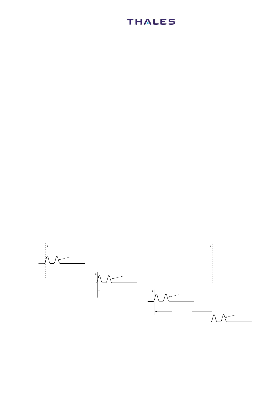
DME (Distance Measuring Equipment) has been standardized by the ICAO as a radio aid for short and
medium-distance navigation. It is a secondary type of radar, which allows several aircraft to simultaneously
measure their distance from a ground reference (DME transponder). The distance is determined by
measuring the propagation delay of a RF pulse, which is emitted by the aircraft transmitter and returned at a
different frequency by the ground station after reception.
In conjunction with a VOR, the DME, which should preferably be installed at the same location as a
VOR/DME, enables to determine the direction and the distance (rho-theta method).
Since the DME operates in the same frequency range (960 to 1215 MHz) and according to the same
principle as the distance measuring section of the TACAN, combined VOR/TACAN systems (VORTAC) are
installed in many countries, as well as VOR/DME systems.
1.2 DME PRINCIPLE
Aircraft's equipped with DME transmit encoded interrogating RF pulse pairs on the beacon's receiving
channel. The beacon, in turn, emits encoded reply pulse pairs on the receiving channel of the air-borne
equipment, which is 63 MHz apart from the transmitter frequency former.
The time interval between interrogation emission and reply reception provides the aircraft with the real
distance information from the ground station; this information may be read by the pilot or the navigator
directly on the airborne indicator.
The ground transponder is able to answer up to about 200 interrogators at a time (i.e. 4800 pulse pairs/s).
Generates random pulse pairs ("squitter") to maintain a minimum PRF of 800 to 2700 pulse pairs per
second (programmable) whenever the number of decoded interrogations is lower than that.
This reply is received and decoded by the airborne receiver, where special timing circuits automatically
measure the lapse between interrogation and reply and convert this measurement into electrical output
signals. The beacon introduces a fixed delay, called reply delay, between the reception of each encoded
interrogating pulse pair and the transmission of the corresponding reply ( see Figure
Travel time (50µs+1µs/150m)
Interrogation Paire pulses
transmitted by aircraft
One way time
1µs/30 0m
Replay Delay of the beacon
Interrogation Paire pulses
received by transponder
(50µs)
Replay delay Pai re pulses
transmitted by transpond er
1.1).
One way time
1µs/30 0m
Replay Paire pulses
received by aircraft
Figure 1.1. DME - Principle of the RF signals path
The transponder periodically transmits special identification pulse groups, interleaved with the reply and
squitter pulses that can be decoded by the aircraft as a Morse tone, keyed with the beacon code name.
Vers. D, September 2005
THALES Italia S.p.A.- A. S. D.
1-1
955 900 031C
DME 415/435 -Technical Manual
Vol. 1-Section 1-General Information
The airborne receiver is able to recognize the replies to its own interrogations, among the many other pulses
transmitted by the beacon, by means of a stroboscopic procedure.
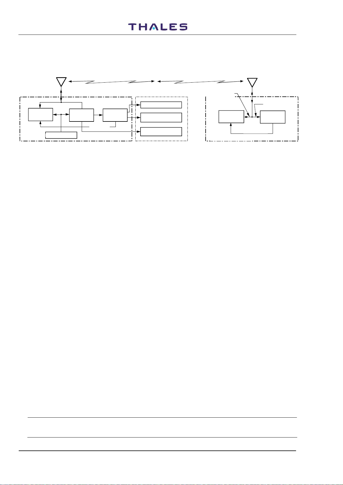
The DME theory of operation is summarized in a block diagram in Figure
AIRCRAFT'S
ANTENNA
AUTOPILOT
TRIGGERS
DISTANCE
CIRCUITS
DISTANCE INFORMATION
TO BOARD INDICATOR
BEACON
IDENTIFICATION TONE
TRANSMITTE R
DME
AIRBORNE
RECEIVER
INTERROGAT ION
CHANNEL SELECTOR
1.2.
TRANSMITS DISTANCE
INFORMATION
and IDENTIFICATION
SIGNAL
TRANSMITTE R
DME GROUND BEACON
BEACON'S
ANTENNA
REPLY TRIGGER TO
INTERROGATI ONS
RECEIVED
INTERROGATIONS
RECEIVER
Figure 1.2. DME - Theory of operation, simplified block diagram
1.2.1 Coverage
According to the frequency band used, the DME system coverage is limited to the optical range and
depends on the aircraft flight altitude and on the type of ground.
The high frequency used and the use of special techniques have made the system much less sensitive to
site errors than other types of omni-directional beacons now in use.
1.2.2 Traffic Capacity
The aircraft handling capacity is adequate for a traffic peak of 200 aircrafts. When the traffic peak exceeds
200 aircrafts the transponder should be capable of handling that peak.
1.2.3 Accuracy
As a result of the development and the applications of modern electronic technologies, the accuracy of the
distance information provided by the DME system is improving all the time.
At present, the accuracy of a DME system can be considered within the maximum values specified below:
±0.12 NM +0.05% of the distance, from 0 to 65 nautical miles, and ± 0.17 NM +0.05% of the distance, above
65 nautical miles.
1.2.4 Nominal Reply Delay – Pair Pulse Code - Channeling
Each beacon is identified by means of its channel frequency, its pulse coding and its identity signal.
The ground beacon introduces a fixed delay between the reception of interrogating pulses and the
transmission of the corresponding reply pulses.
This fixed delay, called main delay or fundamental delay, is introduced. So that an aircraft which is flying
very close to the beacon can complete transmission of the encoded interrogating pulse pair, and then
deactivate its own transmitter, before its receiver begins receiving the corresponding beacon reply pulses.
To render the system as immune as possible to errors caused by interfering signals, the DME system
transmits pulse pairs instead of single pulses; each pair includes two 3.5 µs pulses whose spacing depends
on the channel mode selected.
The channel code, pulse code, reply delay and operating mode are shown on the following table (standard
ICAO).
Channel
Interrogation Pulse Code
Code
X 12
Y 36
Nominal
[µs]
Transponder
Reply Pulse Code
[µs]
12.0 ± 0.1
30.0 ± 0.1
Transponder
Nominal Reply Delay
[µs]
50
56
1-2
THALES Italia S.p.A.- A. S. D.
Vers. D, September 2005
DME 415/435 -Technical Manual
Vol. 1-Section 1-General Information
955 900 031C
Each operational channel in the DME system is defined by two frequencies (interrogation and reply
frequencies), spaced 63 MHz apart, and by the pulse code for the assigned channel (X or Y channel).
The DME system transmits on a pre-selected channel among the 252 available ones. These channels are
divided into 126 X channels and 126 Y channels providing a frequency ranging from 1025 to 1150 MHz for
aircraft transmission (interrogation). Moreover, a 962 to 1213 MHz frequency for signal reception by the
aircraft (ground beacon reply transmission). Interrogation and reply frequencies are assigned with one MHz
spacing between channels.
The diagram shown in figure
frequency for both channel types X, Y. The same information is also given in table
1.3 gives the aircraft interrogation frequency associated to the beacon reply
1-1 and table 1-2 for X
and Y channels respectively, as per ICAO ANNEX 10.
Each beacon emits a Morse identity code signal that can be heard in the pilot headset; this code consists of
pulse pairs transmitted at a frequency of 1350 Hz.
Each beacon is therefore identified by means of its channel frequency, its pulse coding and its identity
signal.
Table 1-1. Frequencies for DME Channels
960 MHz
962 MHz
X Channels (n° 126)
Channel
Y Channels (n° 126)
I = 1025 + (CH-1) I = 1025 + (CH-1)
R = I - 63
R = I + 63
I = INTERROGATION FREQUENCY (MHz) CH = CHANNEL NUMBER
R = REPLY FREQUENCY (MHz)
1025 MHz
1-63X
1 ≤ CH ≤ 63
64 ≤ CH ≤ 126
1088 MHz 1151 MHz
1-63Y
R = I + 63
R = I - 63
64-126X
1215 MHz
1213 MHz
INTERROGATION FREQUENCIES REPLY FREQUENCIES
Vers. D, September 2005
64-126Y
Figure 1.3. DME Channels Reply and Interrogation Frequencies
THALES Italia S.p.A.- A. S. D.
1-3

955 900 031C
DME 415/435 -Technical Manual
Vol. 1-Section 1-General Information
Table 1-2. Frequencies and Code Pulses for DME Channels (1 to 17)
DME PARAMETERS
CHANNEL PAIRING INTERROGATION REPLY
Pulse Codes
DME/P
DME
Channel
1X
1Y
2X
2Y
3X
3Y
4X
4Y
5X
5Y
6X
6Y
7X
7Y
8X
8Y
9X
9Y
10X
10Y
11X
11Y
12X
12Y
13X
13Y
14X
14Y
15X
15Y
16X
16Y
17X
17Y
17Z
VHF
FREQ.
MHz
−
−
−
−
−
−
−
−
−
−
−
−
−
−
−
−
−
−
−
−
−
−
−
−
−
−
−
−
−
−
−
−
108.00
108.05
−
MLS
FREQ.
MHz
−
−
−
−
−
−
−
−
−
−
−
−
−
−
−
−
−
−
−
−
−
−
−
−
−
−
−
−
−
−
−
−
−
5043.0
5043.3
MLS
Channel
−
−
−
−
−
−
−
−
−
−
−
−
−
−
−
−
−
−
−
−
−
−
−
−
−
−
−
−
−
−
−
−
−
540
541
Frequency
MHz
1025
1025
1026
1026
1027
1027
1028
1028
1029
1029
1030
1030
1031
1031
1032
1032
1033
1033
1034
1034
1035
1035
1036
1036
1037
1037
1038
1038
1039
1039
1040
1040
1041
1041
1041
DME/N
µs
12
36
12
36
12
36
12
36
12
36
12
36
12
36
12
36
12
36
12
36
12
36
12
36
12
36
12
36
12
36
12
36
12
36
−
IAM
µs
−
−
−
−
−
−
−
−
−
−
−
−
−
−
−
−
−
−
−
−
−
−
−
−
−
−
−
−
−
−
−
−
−
36
21
FAM
µs
−
−
−
−
−
−
−
−
−
−
−
−
−
−
−
−
−
−
−
−
−
−
−
−
−
−
−
−
−
−
−
−
−
42
27
Frequency
MHz
962
1088
963
1089
964
1090
965
1091
966
1092
967
1093
968
1094
969
1095
970
1096
971
1097
972
1098
973
1099
974
1100
975
1101
976
1102
977
1103
978
1104
1104
Pulse
Codes
µs
12
30
12
30
12
30
12
30
12
30
12
30
12
30
12
30
12
30
12
30
12
30
12
30
12
30
12
30
12
30
12
30
12
30
15
1-4
THALES Italia S.p.A.- A. S. D.
Vers. D, September 2005

DME 415/435 -Technical Manual
Vol. 1-Section 1-General Information
955 900 031C
Table 1-2. Frequencies and Code Pulses for DME Channels (18 to 28)
DME PARAMETERS
CHANNEL PAIRING INTERROGATION REPLY
Pulse Codes
DME/P
DME
Channel
18X
18W
18Y
18Z
19X
19Y
19Z
20X
20W
20Y
20Z
21X
21Y
21Z
22X
22W
22Y
22Z
23X
23Y
23Z
24X
24W
24Y
24Z
25X
25Y
25Z
26X
26W
26Y
26Z
27X
27Y
27Z
28X
28W
28Y
28Z
VHF
FREQ.
MHz
108.10
−
108.15
−
108.20
108.25
−
108.30
−
108.35
−
108.40
108.45
−
108.50
−
108.55
−
108.60
108.65
−
108.70
−
108.75
−
108.80
108.85
−
108.90
−
108.95
−
109.00
109.05
−
109.10
−
109.15
−
MLS
FREQ.
MHz
5031.0
5031.3
5043.6
5043.9
−
5044.2
5044.5
5031.6
5031.9
5044.8
5045.1
−
5045.4
5045.7
5032.2
5032.5
5046.0
5046.3
−
5046.6
5046.9
5032.8
5033.1
5047.2
5047.5
−
5047.8
5048.1
5033.4
5033.7
5048.4
5048.7
−
5049.0
5049.3
5034.0
5034.3
5049.6
5049.9
MLS
Channel
500
501
542
543
−
544
545
502
503
546
547
−
548
549
504
505
550
551
−
552
553
506
507
554
555
−
556
557
508
509
558
559
−
560
561
510
511
562
563
Frequency
MHz
1042
1042
1042
1042
1043
1043
1043
1044
1044
1044
1044
1045
1045
1045
1046
1046
1046
1046
1047
1047
1047
1048
1048
1048
1048
1049
1049
1049
1050
1050
1050
1050
1051
1051
1051
1052
1052
1052
1052
DME/N
µs
12
−
36
−
12
36
−
12
−
36
−
12
36
−
12
−
36
−
12
36
−
12
−
36
−
12
36
−
12
−
36
−
12
36
−
12
−
36
−
IAM
µs
12
24
36
21
−
36
21
12
24
36
21
−
36
21
12
24
36
21
−
36
21
12
24
36
21
−
36
21
12
24
36
21
−
36
21
12
24
36
21
FAM
µs
18
30
42
27
−
42
27
18
30
42
27
−
42
27
18
30
42
27
−
42
27
18
30
42
27
−
42
27
18
30
42
27
−
42
27
18
30
42
27
Frequency
MHz
979
979
1105
1105
980
1106
1106
981
981
1107
1107
982
1108
1108
983
983
1109
1109
984
1110
1110
985
985
1111
1111
986
1112
1112
987
987
1113
1113
988
1114
1114
989
989
1115
1115
Pulse
Codes
µs
12
24
30
15
12
30
15
12
24
30
15
12
30
15
12
24
30
15
12
30
15
12
24
30
15
12
30
15
12
24
30
15
12
30
15
12
24
30
15
Vers. D, September 2005
THALES Italia S.p.A.- A. S. D.
1-5

955 900 031C
DME 415/435 -Technical Manual
Vol. 1-Section 1-General Information
Table 1-2. Frequencies and Code Pulses for DME Channels (29 to 40)
DME PARAMETERS
CHANNEL PAIRING INTERROGATION REPLY
Pulse Codes
DME/P
DME
Channel
29X
29Y
29Z
30X
30W
30Y
30Z
31X
31Y
31Z
32X
32W
32Y
32Z
33X
33Y
33Z
34X
34W
34Y
34Z
35X
35Y
35Z
36X
36W
36Y
36Z
37X
37Y
37Z
38X
38W
38Y
38Z
39X
39Y
39Z
40X
40W
40Y
40Z
VHF
FREQ.
MHz
109.20
109.25
−
109.30
−
109.35
−
109.40
109.45
−
109.50
−
109.55
−
109.60
109.65
−
109.70
−
109.75
−
109.80
109.85
−
109.90
−
109.95
−
110.00
110.05
−
110.10
−
110.15
−
110.20
110.25
−
110.30
−
110.35
−
MLS
FREQ.
MHz
−
5050.2
5050.5
5034.6
5034.9
5050.8
5051.1
−
5051.4
5051.7
5035.2
5035.5
5052.0
5052.3
−
5052.6
5052.9
5035.8
5036.1
5053.2
5053.5
−
5053.8
5054.1
5036.4
5036.7
5054.4
5054.7
−
5055.0
5055.3
5037.0
5037.3
5055.6
5055.9
−
5056.2
5056.5
5037.6
5037.9
5056.8
5057.1
MLS
Channel
−
564
565
512
513
566
567
−
568
569
514
515
570
571
−
572
573
516
517
574
575
−
576
577
518
519
578
579
−
580
581
520
521
582
583
−
584
585
522
523
586
587
Frequency
MHz
1053
1053
1053
1054
1054
1054
1054
1055
1055
1055
1056
1056
1056
1056
1057
1057
1057
1058
1058
1058
1058
1059
1059
1059
1060
1060
1060
1060
1061
1061
1061
1062
1062
1062
1062
1063
1063
1063
1064
1064
1064
1064
DME/N
µs
12
36
−
12
−
36
−
12
36
−
12
−
36
−
12
36
−
12
−
36
−
12
36
−
12
−
36
−
12
36
−
12
−
36
−
12
36
−
12
−
36
−
IAM
µs
−
36
21
12
24
36
21
−
36
21
12
24
36
21
−
36
21
12
24
36
21
−
36
21
12
24
36
21
−
36
21
12
24
36
21
−
36
21
12
24
36
21
FAM
µs
−
42
27
18
30
42
27
−
42
27
18
30
42
27
−
42
27
18
30
42
27
−
42
27
18
30
42
27
−
42
27
18
30
42
27
−
42
27
18
30
42
27
Frequency
MHz
990
1116
1116
991
991
1117
1117
992
1118
1118
993
993
1119
1119
994
1120
1120
995
995
1121
1121
996
1122
1122
997
997
1123
1123
998
1124
1124
999
999
1125
1125
1000
1126
1126
1001
1001
1127
1127
Pulse
Codes
µs
12
30
15
12
24
30
15
12
30
15
12
24
30
15
12
30
15
12
24
30
15
12
30
15
12
24
30
15
12
30
15
12
24
30
15
12
30
15
12
24
30
15
1-6
THALES Italia S.p.A.- A. S. D.
Vers. D, September 2005

DME 415/435 -Technical Manual
Vol. 1-Section 1-General Information
955 900 031C
Table 1-2. Frequencies and Code Pulses for DME Channels (41 to 52)
DME PARAMETERS
CHANNEL PAIRING INTERROGATION REPLY
Pulse Codes
DME/P
DME
Channel
41X
41Y
41Z
42X
42W
42Y
42Z
43X
43Y
43Z
44X
44W
44Y
44Z
45X
45Y
45Z
46X
46W
46Y
46Z
47X
47Y
47Z
48X
48W
48Y
48Z
49X
49Y
49Z
50X
50W
50Y
50Z
51X
51Y
51Z
52X
52W
52Y
52Z
VHF
FREQ.
MHz
110.40
110.45
−
110.50
−
110.55
−
110.60
110.65
−
110.70
−
110.75
−
110.80
110.85
−
110.90
−
110.95
−
111.00
111.05
−
111.10
−
111.15
−
111.20
111.25
−
111.30
−
111.35
−
111.40
111.45
−
111.50
−
111.55
−
MLS
FREQ.
MHz
−
5057.4
5057.7
5038.2
5038.5
5058.0
5058.3
−
5058.6
5058.9
5038.8
5039.1
5059.2
5059.5
−
5059.8
5060.1
5039.4
5039.7
5060.4
5060.7
−
5061.0
5061.3
5040.0
5040.3
5061.6
5061.9
−
5062.2
5062.5
5040.6
5040.9
5062.8
5063.1
−
5063.4
5063.7
5041.2
5041.5
5064.0
5064.3
MLS
Channel
−
588
589
524
525
590
591
−
592
593
526
527
594
595
−
596
597
528
529
598
599
−
600
601
530
531
602
603
−
604
605
532
533
606
607
−
608
609
534
535
610
611
Frequency
MHz
1065
1065
1065
1066
1066
1066
1066
1067
1067
1067
1068
1068
1068
1068
1069
1069
1069
1070
1070
1070
1070
1071
1071
1071
1072
1072
1072
1072
1073
1073
1073
1074
1074
1074
1074
1075
1075
1075
1076
1076
1076
1076
DME/N
µs
12
36
−
12
−
36
−
12
36
−
12
−
36
−
12
36
−
12
−
36
−
12
36
−
12
−
36
−
12
36
−
12
−
36
−
12
36
−
12
−
36
−
IAM
µs
−
36
21
12
24
36
21
−
36
21
12
24
36
21
−
36
21
12
24
36
21
−
36
21
12
24
36
21
−
36
21
12
24
36
21
−
36
21
12
24
36
21
FAM
µs
−
42
27
18
30
42
27
−
42
27
18
30
42
27
−
42
27
18
30
42
27
−
42
27
18
30
42
27
−
42
27
18
30
42
27
−
42
27
18
30
42
27
Frequency
MHz
1002
1128
1128
1003
1003
1129
1129
1004
1130
1130
1005
1005
1131
1131
1006
1132
1132
1007
1007
1133
1133
1008
1134
1134
1009
1009
1135
1135
1010
1136
1136
1011
1011
1137
1137
1012
1138
1138
1013
1013
1139
1139
Pulse
Codes
µs
12
30
15
12
24
30
15
12
30
15
12
24
30
15
12
30
15
12
24
30
15
12
30
15
12
24
30
15
12
30
15
12
24
30
15
12
30
15
12
24
30
15
Vers. D, September 2005
THALES Italia S.p.A.- A. S. D.
1-7

955 900 031C
DME 415/435 -Technical Manual
Vol. 1-Section 1-General Information
Table 1-2. Frequencies and Code Pulses for DME Channels (53 to 68)
DME PARAMETERS
CHANNEL PAIRING INTERROGATION REPLY
Pulse Codes
DME/P
DME
Channel
53X
53Y
53Z
54X
54W
54Y
54Z
55X
55Y
55Z
56X
56W
56Y
56Z
57X
57Y
58X
58Y
59X
59Y
60X
60Y
61X
61Y
62X
62Y
63X
63Y
64X
64Y
65X
65Y
66X
66Y
67X
67Y
68X
68Y
VHF
FREQ.
MHz
111.60
111.65
−
111.70
−
111.75
−
111.80
111.85
−
111.90
−
111.95
−
112.00
112.05
112.10
112.15
112.20
112.25
−
−
−
−
−
−
−
−
−
−
−
−
−
−
−
−
−
−
MLS
FREQ.
MHz
−
5064.5
5064.9
5041.8
5042.1
5065.2
5065.5
−
5065.8
5066.1
5042.4
5042.7
5066.4
5066.7
−
−
−
−
−
−
−
−
−
−
−
−
−
−
−
−
−
−
−
−
−
−
−
−
MLS
Channel
−
612
613
536
537
614
615
−
616
617
538
539
618
619
−
−
−
−
−
−
−
−
−
−
−
−
−
−
−
−
−
−
−
−
−
−
−
−
Frequency
MHz
1077
1077
1077
1078
1078
1078
1078
1079
1079
1079
1080
1080
1080
1080
1081
1081
1082
1082
1083
1083
1084
1084
1085
1085
1086
1086
1087
1087
1088
1088
1089
1089
1090
1090
1091
1091
1092
1092
DME/N
µs
12
36
−
12
−
36
−
12
36
−
12
−
36
−
12
36
12
36
12
36
12
36
12
36
12
36
12
36
12
36
12
36
12
36
12
36
12
36
IAM
µs
−
36
21
12
24
36
21
−
36
21
12
24
36
21
−
−
−
−
−
−
−
−
−
−
−
−
−
−
−
−
−
−
−
−
−
−
−
−
FAM
µs
−
42
27
18
30
42
27
−
42
27
18
30
42
27
−
−
−
−
−
−
−
−
−
−
−
−
−
−
−
−
−
−
−
−
−
−
−
−
Frequency
MHz
1014
1140
1140
1015
1015
1141
1141
1016
1142
1142
1017
1017
1143
1143
1018
1144
1019
1145
1020
1146
1021
1147
1022
1148
1023
1149
1024
1150
1151
1025
1152
1026
1153
1027
1154
1028
1155
1029
Pulse
Codes
µs
12
30
15
12
24
30
15
12
30
15
12
24
30
15
12
30
12
30
12
30
12
30
12
30
12
30
12
30
12
30
12
30
12
30
12
30
12
30
1-8
THALES Italia S.p.A.- A. S. D.
Vers. D, September 2005

DME 415/435 -Technical Manual
Vol. 1-Section 1-General Information
955 900 031C
Table 1-2. Frequencies and Code Pulses for DME Channels (69 to 85)
DME PARAMETERS
CHANNEL PAIRING INTERROGATION REPLY
Pulse Codes
DME/P
DME
Channel
69X
69Y
70X
70Y
71X
71Y
72X
72Y
73X
73Y
74X
74Y
75X
75Y
76X
76Y
77X
77Y
78Y
78Y
79X
79Y
80X
80Y
80Z
81X
81Y
81Z
82X
82Y
82Z
83X
83Y
83Z
84X
84Y
84Z
85X
85Y
85Z
VHF
FREQ.
MHz
−
−
112.30
112.35
112.40
112.45
112.50
112.55
112.60
112.65
112.70
112.75
112.80
112.85
112.90
112.95
113.00
113.05
113.10
113.15
113.20
113.25
113.30
113.35
−
113.40
113.45
−
113.50
113.55
−
113.60
113.65
−
113.70
113.75
−
113,80
113,85
-
MLS
FREQ.
MHz
−
−
−
−
−
−
−
−
−
−
−
−
−
−
−
−
−
−
−
−
−
−
−
5067.0
5067.3
−
5067.6
5067.9
−
5068.2
5068.5
−
5068.8
5069.1
−
5069.4
5069.7
5070.0
5071.3
MLS
Channel
−
−
−
−
−
−
−
−
−
−
−
−
−
−
−
−
−
−
−
−
−
−
−
620
621
−
622
623
−
624
625
−
626
627
−
628
629
1109
Frequency
MHz
1093
1093
1094
1094
1095
1095
1096
1096
1097
1097
1098
1098
1099
1099
1100
1100
1101
1101
1102
1102
1103
1103
1104
1104
1104
1105
1105
1105
1106
1106
1106
1107
1107
1107
1108
1108
1108
1109
1109
DME/N
µs
12
36
12
36
12
36
12
36
12
36
12
36
12
36
12
36
12
36
12
36
12
36
12
36
−
12
36
−
12
36
−
12
36
−
12
36
−
12
36
-
IAM
µs
−
−
−
−
−
−
−
−
−
−
−
−
−
−
−
−
−
−
−
−
−
−
−
36
21
−
36
21
−
36
21
−
36
21
−
36
21
36
21
FAM
µs
−
−
−
−
−
−
−
−
−
−
−
−
−
−
−
−
−
−
−
−
−
−
−
42
27
−
42
27
−
42
27
−
42
27
−
42
27
42
27
Frequency
MHz
1156
1030
1157
1031
1158
1032
1159
1033
1160
1034
1161
1035
1162
1036
1163
1037
1164
1038
1165
1039
1166
1040
1167
1041
1041
1168
1042
1042
1169
1043
1043
1170
1044
1044
1171
1045
1045
1172
1046
1046
Pulse
Codes
µs
12
30
12
30
12
30
12
30
12
30
12
30
12
30
12
30
12
30
12
30
12
30
12
30
15
12
30
15
12
30
15
12
30
15
12
30
15
12
30
15
Vers. D, September 2005
THALES Italia S.p.A.- A. S. D.
1-9

955 900 031C
DME 415/435 -Technical Manual
Vol. 1-Section 1-General Information
Table 1-2. Frequencies and Code Pulses for DME Channels (86 to 99)
DME PARAMETERS
CHANNEL PAIRING INTERROGATION REPLY
Pulse Codes
DME/P
DME
Channel
86X
86Y
86Z
87X
87Y
87Z
88X
88Y
88Z
89X
89Y
89Z
90X
90Y
90Z
91X
91Y
91Z
92X
92Y
92Z
93X
93Y
93Z
94X
94Y
94Z
95X
95Y
95Z
96X
96Y
96Z
97X
97Y
97Z
98X
98Y
98Z
99X
99Y
99Z
VHF
FREQ.
MHz
113.90
113.95
−
114.00
114.05
−
114.10
114.15
−
114.20
114.25
−
114.30
114.35
−
114.40
114.45
−
114.50
114.55
−
114.60
114.65
−
114.70
114.75
−
114.80
114.85
−
114.90
114.95
−
115.00
115.05
−
115.10
115.15
−
115.20
115.25
−
MLS
FREQ.
MHz
−
5070.6
5070.9
−
5071.2
5071.5
−
5071.8
5072.1
−
5072.4
5072.7
−
5073.0
5073.3
−
5073.6
5073.9
−
5074.2
5074.5
−
5074.8
5075.1
−
5075.4
5075.7
−
5076.0
5076.3
−
5076.6
5076.9
−
5077.2
5077.5
−
5077.8
5078.1
−
5078.4
5078.7
MLS
Channel
−
632
633
−
634
635
−
636
637
−
638
639
−
640
641
−
642
643
−
644
645
−
646
647
−
648
649
−
650
651
−
652
653
−
654
655
−
656
657
−
658
659
Frequency
MHz
1110
1110
1110
1111
1111
1111
1112
1112
1112
1113
1113
1113
1114
1114
1114
1115
1115
1115
1116
1116
1116
1117
1117
1117
1118
1118
1118
1119
1119
1119
1120
1120
1120
1121
1121
1121
1122
1122
1122
1123
1123
1123
DME/N
µs
12
36
−
12
36
−
12
36
−
12
36
−
12
36
−
12
36
−
12
36
−
12
36
−
12
36
−
12
36
−
12
36
−
12
36
−
12
36
−
12
36
−
IAM
µs
−
36
21
−
36
21
−
36
21
−
36
21
−
36
21
−
36
21
−
36
21
−
36
21
−
36
21
−
36
21
−
36
21
−
36
21
−
36
21
−
36
21
FAM
µs
−
42
27
−
42
27
−
42
27
−
42
27
−
42
27
−
42
27
−
42
27
−
42
27
−
42
27
−
42
27
−
42
27
−
42
27
−
42
27
−
42
27
Frequency
MHz
1173
1047
1047
1174
1048
1048
1175
1049
1049
1176
1050
1050
1177
1051
1051
1178
1052
1052
1179
1053
1053
1180
1054
1054
1181
1055
1055
1182
1056
1056
1183
1057
1057
1184
1058
1058
1185
1059
1059
1186
1060
1060
Pulse
Codes
µs
12
30
15
12
30
15
12
30
15
12
30
15
12
30
15
12
30
15
12
30
15
12
30
15
12
30
15
12
30
15
12
30
15
12
30
15
12
30
15
12
30
15
1-10
THALES Italia S.p.A.- A. S. D.
Vers. D, September 2005
 Loading...