

Page 1
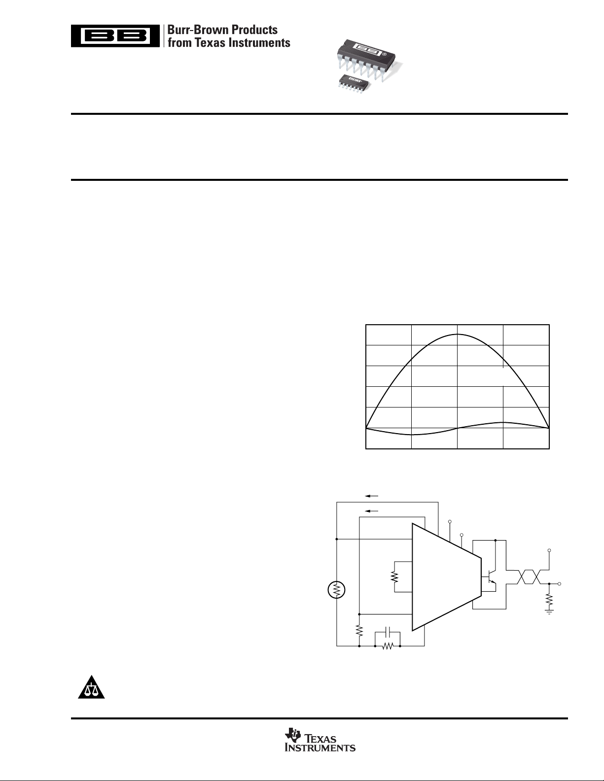
–200°C
Pt100 NONLINEARITY CORRECTION
USING XTR105
Process Temperature (°C)
+850°C
5
4
3
2
1
0
–1
Uncorrected
RTD Nonlinearity
Corrected
Nonlinearity
Nonlinearity (%)
XTR105
XTR105
XTR105
SBOS061B – FEBRUARY 1997 – REVISED AUGUST 2004
4-20mA CURRENT TRANSMITTER
with Sensor Excitation and Linearization
FEATURES
● LOW UNADJUSTED ERROR
● TWO PRECISION CURRENT SOURCES: 800µA each
● LINEARIZATION
● 2- OR 3-WIRE RTD OPERATION
● LOW OFFSET DRIFT: 0.4µV/°C
● LOW OUTPUT CURRENT NOISE: 30nA
PP
APPLICATIONS
● INDUSTRIAL PROCESS CONTROL
● FACTORY AUTOMATION
● SCADA REMOTE DATA ACQUISITION
● REMOTE TEMPERATURE AND PRESSURE
TRANSDUCERS
● HIGH PSR: 110dB minimum
● HIGH CMR: 86dB minimum
● WIDE SUPPLY RANGE: 7.5V to 36V
● DIP-14 AND SO-14 PACKAGES
DESCRIPTION
The XTR105 is a monolithic 4-20mA, 2-wire current transmitter with two precision current sources. It provides complete
current excitation for platinum RTD temperature sensors and
bridges, instrumentation amplifiers, and current output circuitry on a single integrated circuit.
Versatile linearization circuitry provides a 2nd-order correction to the RTD, typically achieving a 40:1 improvement in
linearity.
Instrumentation amplifier gain can be configured for a wide
range of temperature or pressure measurements. Total unadjusted error of the complete current transmitter is low
enough to permit use without adjustment in many applications. This includes zero output current drift, span drift, and
nonlinearity. The XTR105 operates on loop power-supply
voltages down to 7.5V.
RTD
The XTR105 is available in DIP-14 and SO-14 surfacemount packages and is specified for the –40°C to +85°C
industrial temperature range.
= 0.8mA
I
R
IR = 0.8mA
R
G
+
–
V
LIN
XTR105
V
REG
7.5V to 36V
4-20 mA
V
PS
V
O
R
L
Please be aware that an important notice concerning availability, standard warranty, and use in critical applications of
Texas Instruments semiconductor products and disclaimers thereto appears at the end of this data sheet.
All trademarks are the property of their respective owners.
PRODUCTION DATA information is current as of publication date.
Products conform to specifications per the terms of Texas Instruments
standard warranty. Production processing does not necessarily include
testing of all parameters.
Copyright © 1997-2004, Texas Instruments Incorporated
www.ti.com
Page 2
ABSOLUTE MAXIMUM RATINGS
(1)
Power Supply, V+ (referenced to the IO pin)...................................... 40V
, V
Input Voltage, V
(referenced to the IO pin) ....................0V to V+
IN+
IN–
Storage Temperature Range ......................................... –55°C to +125°C
Lead Temperature (soldering, 10s) ............................................... +300°C
Output Current Limit ................................................................ Continuous
Junction Temperature .................................................................... +165°C
NOTE: (1) Stresses above those listed under “Absolute Maximum Ratings”
may cause permanent damage to the device. Exposure to absolute maximum
conditions for extended periods may affect device reliability.
ELECTROSTATIC
DISCHARGE SENSITIVITY
This integrated circuit can be damaged by ESD. Texas Instruments recommends that all integrated circuits be handled with
appropriate precautions. Failure to observe proper handling
and installation procedures can cause damage.
ESD damage can range from subtle performance degradation to complete device failure. Precision integrated circuits
may be more susceptible to damage because very small
parametric changes could cause the device not to meet its
published specifications.
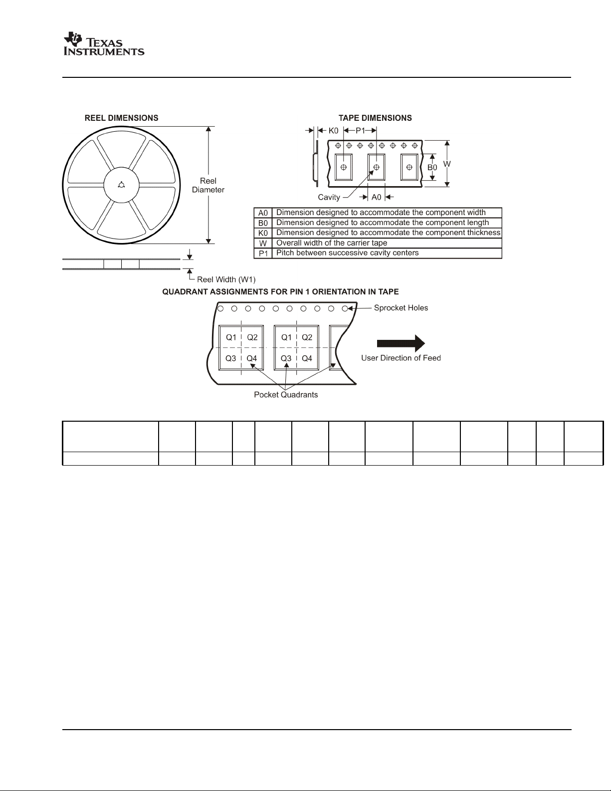
PACKAGE/ORDERING INFORMATION
(1)
SPECIFIED
PACKAGE TEMPERATURE PACKAGE ORDERING TRANSPORT
PRODUCT PACKAGE-LEAD DESIGNATOR RANGE MARKING NUMBER MEDIA, QUANTITY
XTR105 DIP-14 N –40°C to +85°C XTR105PA XTR105PA Rails, 25
" """XTR105P XTR105P Rails, 25
XTR105 SO-14 Surface-Mount D –40°C to +85°C XTR105UA XTR105UA Rails, 58
" """XTR105UA XTR105UA/2K5 Tape and Reel, 2500
XTR105 SO-14 Surface-Mount D –40°C to +85°C XTR105U XTR105U Rails, 58
" """XTR105U XTR105U/2K5 Tape and Reel, 2500
NOTE: (1) For the most current package and ordering information, see the Package Option Addendum located at the end of this data sheet.
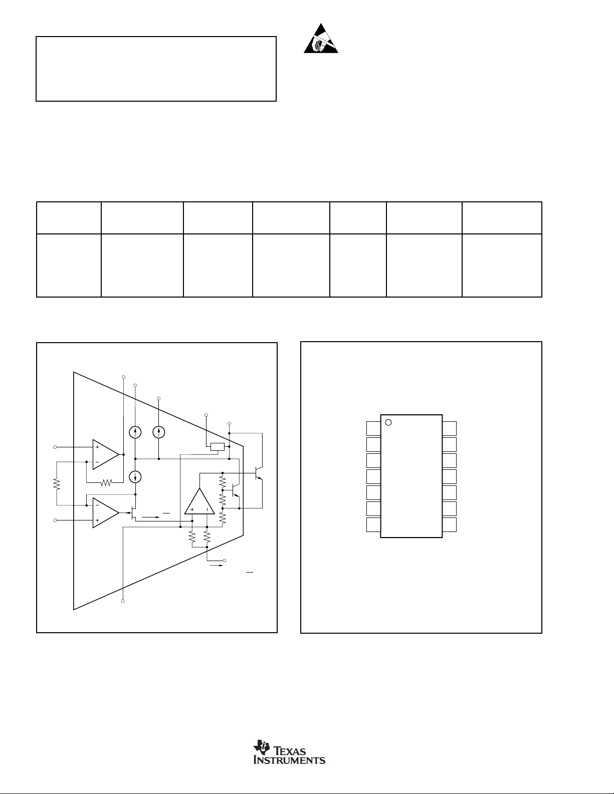
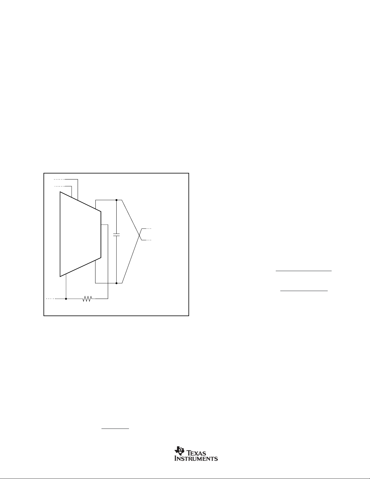
FUNCTIONAL BLOCK DIAGRAM
V
LIN
I
R1
12
13
+
V
IN
4
R
LIN
R
G
3
2
–
V
IN
1kΩ
6
I
RET
I
R2
1
14
800µA 800µA
100µA
V
I = 100µA +
R
IN
G
975Ω
V
REG
11
5.1V
25Ω
7
IO = 4mA + V
V+
10
B
Q
1
9
E
8
40
•
( )
IN
R
G
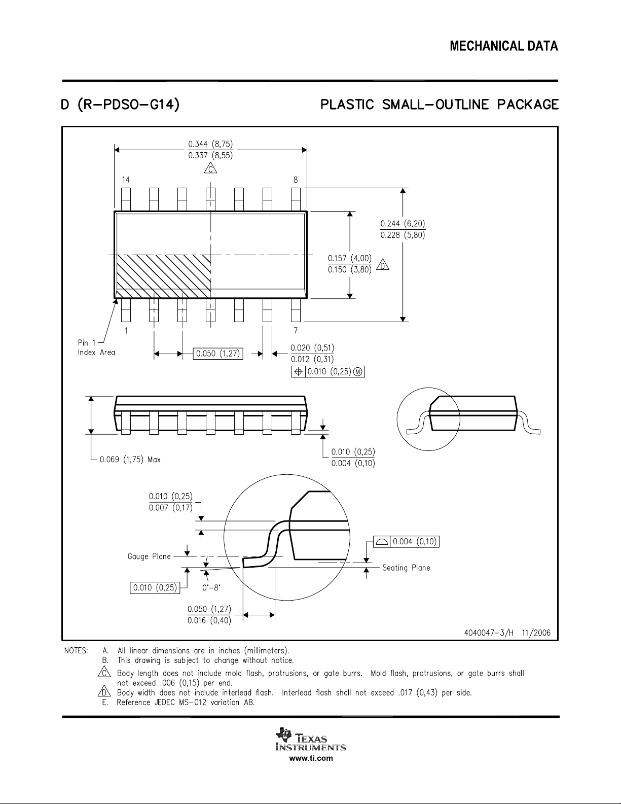
PIN CONFIGURATION
Top View DIP and SO
1
I
R1
– +
2
VIN
3
R
G
4
R
G
5
NC
6
I
RET
7
I
O
NC = No Internal Connection
14
13
12
11
10
9
8
I
R2
V
IN
V
LIN
V
REG
V+
B (Base)
E (Emitter)
2
www.ti.com
XTR105
SBOS061B
Page 3

ELECTRICAL CHARACTERISTICS
At TA = +25°C, V+ = 24V, and TIP29C external transistor, unless otherwise noted.
XTR105P, U XTR105PA, UA
PARAMETER CONDITIONS MIN TYP MAX MIN TYP MAX UNITS
OUTPUT
Output Current Equation A
Output Current, Specified Range 4 20 ✻✻mA
Over-Scale Limit 24 27 30 ✻✻✻ mA
Under-Scale Limit I
ZERO OUTPUT
(1)
= 0V 1.8 2.2 2.6 ✻✻✻ mA
REG
VIN = 0V, RG = ∞ 4 ✻ mA
Initial Error ±5 ±25 ✻ ±50 µA
vs Temperature ±0.07 ±0.5 ✻ ±0.9 µA/°C
vs Supply Voltage, V+ V+ = 7.5V to 36V 0.04 0.2 ✻✻ µA/V
vs Common-Mode Voltage
vs V
Output Current 0.3 ✻ µA/mA
REG
Noise, 0.1Hz to 10Hz 0.03 ✻ µA
VCM = 1.25V to 3.5V
(2)
SPAN
Span Equation (transconductance)
Initial Error
vs Temperature
Nonlinearity, Ideal Input
INPUT
(3)
(3)
(4)
(5)
Full-Scale (VIN) = 50mV ±0.05 ±0.2 ✻ ±0.4 %
Full-Scale (VIN) = 50mV 0.003 0.01 ✻✻ %
Offset Voltage VCM = 2V ±50 ±100 ✻ ±250 µV
vs Temperature ±0.4 ±1.5 ✻ ±3 µV/°C
vs Supply Voltage, V+ V+ = 7.5V to 36V ±0.3 ±3 ✻✻ µV/V
vs Common-Mode Voltage, VCM = 1.25V to 3.5V
RTI (CMRR)
Common-Mode Input Range
(2)
(2)
Input Bias Current 525 ✻ 50 nA
vs Temperature 20 ✻ pA/°C
Input Offset Current ±0.2 ±3 ✻ ±10 nA
vs Temperature 5 ✻ pA/°C
Impedance, Differential 0.1 || 1 ✻ GΩ || pF
Common-Mode 5 || 10 ✻ GΩ || pF
Noise, 0.1Hz to 10Hz 0.6 ✻ µV
CURRENT SOURCES VO = 2V
(6)
Current 800 ✻ µA
Accuracy ±0.05 ±0.2 ✻ ±0.4 %
vs Temperature ±15 ±35 ✻ ±75 ppm/°C
vs Power Supply, V+ V+ = 7.5V to 36V ±10 ±25 ✻✻ ppm/V
Matching ±0.02 ±0.1 ✻ ±0.2 %
vs Temperature ±3 ±15 ✻ ±30 ppm/°C
vs Power Supply, V+ V+ = 7.5V to 36V 1 10 ✻✻ ppm/V
Compliance Voltage, Positive (V+) – 3
Negative
(2)
Output Impedance 150 ✻ MΩ
Noise, 0.1Hz to 10Hz 0.003 ✻ µA
(2)
V
REG
Accuracy ±0.02 ±0.1 ✻✻ V
vs Temperature ±0.2 ✻ mV/°C
vs Supply Voltage, V+ 1 ✻ mV/V
Output Current ±1 ✻ mA
Output Impedance 75 ✻ Ω
LINEARIZATION
R
(internal) 1 ✻ kΩ
LIN
Accuracy ±0.2 ±0.5 ✻ ±1%
vs Temperature ±25 ±100 ✻✻ ppm/°C
POWER SUPPLY
Specified +24 ✻ V
Voltage Range +7.5 +36 ✻✻V
TEMPERATURE RANGE
Specification, T
Operating –55 +125 ✻✻°C
MIN
to T
MAX
Storage –55 +125 ✻✻°C
Thermal Resistance,
DIP-14 80 ✻ °C/W
θ
JA
SO-14 Surface-Mount 100 ✻ °C/W
✻ Specification same as XTR105P and XTR105U.
NOTES: (1) Describes accuracy of the 4mA low-scale offset current. Does not include input amplifier effects. Can be trimmed to zero.
(2) Voltage measured with respect to I
(3) Does not include initial error or TCR of gain-setting resistor, R
RET
pin.
(4) Increasing the full-scale input range improves nonlinearity.
(5) Does not include Zero Output initial error.
(6) Current source output voltage with respect to I
RET
pin.
IO = VIN • (40/RG) + 4mA, VIN in Volts, RG in Ω
0.02 ✻ µA/V
S = 40/R
G
✻ A/V
±3 ±25 ✻✻ ppm/°C
±10 ±50 ✻ ±100 µV/V
1.25 3.5 ✻✻V
(V+) – 2.5
✻✻ V
0 –0.2 ✻✻ V
5.1 ✻ V
–40 +85 ✻✻°C
.
G
PP
PP
PP
XTR105
SBOS061B
www.ti.com
3
Page 4
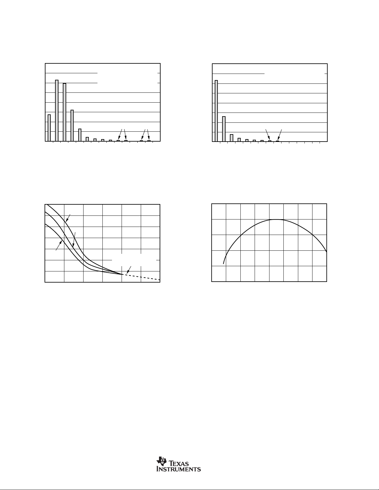
TYPICAL CHARACTERISTICS
At TA = +25°C and V+ = 24V, unless otherwise noted.
50
40
30
20
10
Transconductance (20 Log mA/V)
0
100 1k 10k 100k
110
100
90
80
70
60
50
40
Common-Mode Rejection (dB)
30
20
TRANSCONDUCTANCE vs FREQUENCY
RG = 500Ω
RG = 2kΩ
Frequency (Hz)
COMMON-MODE REJECTION vs FREQUENCY
Full-Scale Input = 50mV
RG = 2kΩ
10 100 1k 10k 100k
Frequency (Hz)
R
G
= 125Ω
RG = 125Ω
1M
1M
STEP RESPONSE
RG = 2kΩ
20mA
RG = 125Ω
4mA/div
4mA
25µs/div
140
120
100
80
60
40
Power Supply Rejection (dB)
20
POWER-SUPPLY REJECTION vs FREQUENCY
RG = 2kΩ
0
10 100 1k 10k 100k
Frequency (Hz)
RG = 125Ω
1M
29
28
27
V+ = 36V
26
25
Over-Scale Current (mA)
24
23
–75 –50 –25 0 25 50 75 100
4
OVER-SCALE CURRENT vs TEMPERATURE
With External Transistor
V+ = 7.5V
V+ = 24V
Temperature (°C)
125
www.ti.com
2.40
2.35
2.30
2.25
Under-Scale Current (mA)
2.20
2.15
UNDER-SCALE CURRENT vs TEMPERATURE
V+ = 7.5V to 36V
–75 –50 –25 0 25 50 75 100
Temperature (°C)
125
XTR105
SBOS061B
Page 5
TYPICAL CHARACTERISTICS (Cont.)
–75 –50 –25 0 25 50 75 100
Temperature (°C)
ZERO OUTPUT CURRENT ERROR
vs TEMPERATURE
125
4
2
0
–2
–4
–6
–8
–10
–12
Zero Output Current Error (µA)
At TA = +25°C and V+ = 24V, unless otherwise noted.
INPUT VOLTAGE AND CURRENT
NOISE DENSITY vs FREQUENCY
10k
1k
100
Input Voltage Noise (nV/√Hz)
10
1 10 100 1k 10k
Frequency (Hz)
INPUT BIAS AND OFFSET CURRENT
vs TEMPERATURE
25
20
15
Current Noise
Voltage Noise
ZERO OUTPUT AND REFERENCE
10k
1k
100
Input Current Noise (fA/√Hz)
10
100k
+I
B
10k
1k
100
Noise (pA/√Hz)
10
1 10 100 1k 10k
CURRENT NOISE vs FREQUENCY
Zero Output Current
Reference Current
100k
Frequency (Hz)
10
5
Input Bias and Offset Current (nA)
0
–75 –50 –25 0 25 50 75 100
INPUT OFFSET VOLTAGE DRIFT
50
45
40
35
30
25
20
15
Percent of Units (%)
10
5
0
0.2
XTR105
SBOS061B
PRODUCTION DISTRIBUTION
0.4
0.6
0.8
Input Offset Voltage Drift (µV/°C)
Temperature (°C)
Typical Production Distribution
0.1%
1.0
1.2
1.4
1.6
1.8
I
OS
of Packaged Units.
0.02%
2.0
2.2
2.4
2.6
2.8
–I
B
125
3.0
www.ti.com
40
35
30
25
20
15
Percent of Units (%)
10
5
0
0.025
0.050
0.075
ZERO OUTPUT DRIFT
PRODUCTION DISTRIBUTION
Typical Production Distribution
0.100
0.125
0.150
0.175
0.200
0.225
0.250
0.275
0.300
Zero Output Drift (µA/°C)
of Packaged Units.
0.325
0.350
0.375
0.400
0.425
0.450
0.475
0.500
5
Page 6
TYPICAL CHARACTERISTICS (Cont.)
At TA = +25°C and V+ = 24V, unless otherwise noted.
40
35
30
25
20
15
Percent of Units (%)
10
5
0
5
10152025303540455055606570
OUTPUT VOLTAGE vs V
V
REG
5.35
5.30
5.25
5.20
125°C
CURRENT SOURCE DRIFT
PRODUCTION DISTRIBUTION
Typical Production Distribution
Current Source Drift (ppm/°C)
25°C
of Packaged Units.
I
AND IR2 Included.
R1
0.04%
OUTPUT CURRENT
REG
0.01%
CURRENT SOURCE MATCHING
80
70
60
50
40
30
Percent of Units (%)
20
10
0
75
+0.05
0
–0.05
DRIFT PRODUCTION DISTRIBUTION
Typical Production Distribution
0.07%
2
4
6
8
1012141618202224262830
Current Source Matching Drift (ppm/°C)
REFERENCE CURRENT ERROR
vs TEMPERATURE
of Packaged Units.
0.02%
5.15
Output Voltage (V)
REG
V
–55°C
5.10
5.05
5.00
–1.0 –0.5 0 0.5 1.0 1.5
Output Current (mA)
V
REG
NOTE: Above 1mA,
Zero Output Degrades
2.0
–0.10
–0.15
Reference Current Error (%)
–0.20
–75 –50 –25 0 25 50 75 100 125
Temperature (°C)
6
www.ti.com
XTR105
SBOS061B
Page 7

APPLICATION INFORMATION
Figure 1 shows the basic connection diagram for the XTR105.
The loop power supply, V
Output loop current is measured as a voltage across the
series load resistor, R
Two matched 0.8mA current sources drive the RTD and
zero-setting resistor, RZ. The instrumentation amplifier input
of the XTR105 measures the voltage difference between the
RTD and R
. The value of RZ is chosen to be equal to the
Z
resistance of the RTD at the low-scale (minimum) measurement temperature. R
at the minimum measurement temperature to correct for
input offset voltage and reference current mismatch of the
XTR105.
RCM provides an additional voltage drop to bias the inputs of
the XTR105 within their common-mode input range. R
should be bypassed with a 0.01µF capacitor to minimize
common-mode noise. Resistor R
mentation amplifier according to the desired temperature
range. R
provides 2nd-order linearization correction to the
LIN1
RTD, typically achieving a 40:1 improvement in linearity. An
additional resistor is required for 3-wire RTD connections
(see Figure 3).
, provides power for all circuitry.
PS
.
L
can be adjusted to achieve 4mA output
Z
sets the gain of the instru-
G
CM
The transfer function through the complete instrumentation
amplifier and voltage-to-current converter is:
IO = 4mA + V
in volts, RG in ohms)
(V
IN
where V
is the differential input voltage.
IN
As evident from the transfer function, if no R
• (40/RG)
IN
is used the
G
gain is zero and the output is simply the XTR105’s zero
current. The value of R
wire RTD connections with linearization. R
varies slightly for 2-wire RTD and 3-
G
can be calcu-
G
lated from the equations given in Figure 1 (2-wire RTD
connection) and Table I (3-wire RTD connection).
The I
sources and V
pin is the return path for all current from the current
RET
REG
. The I
pin allows any current used in
RET
external circuitry to be sensed by the XTR105 and to be
included in the output current without causing an error.
The V
pin provides an on-chip voltage source of approxi-
REG
mately 5.1V and is suitable for powering external input
circuitry (refer to Figure 6). It is a moderately accurate
voltage reference—it is not the same reference used to set
the 800µA current references. V
is capable of sourcing
REG
approximately 1mA of current. Exceeding 1mA may affect
the 4mA zero output.
RTD
IR = 0.8mA
IR = 0.8mA
12
1
V
LIN
13
+
V
IN
4
R
G
(2)
R
G
3
(3)
R
LIN1
(1)
R
Z
RCM = 1kΩ
0.01µF
R
G
–
V
2
IN
I
RET
6
I
R1
I
R2
XTR105
14
11
V
REG
V+
I
O
7.5V to 36V
10
9
B
E
7
Q
1
8
I = 4mA + V
O
NOTES: (1) RZ = RTD resistance at minimum measured temperature.
Possible choices for Q
0.01µF
40
• ( )
IN
R
G
(2)
RG =
(3)
=
R
LIN1
= RTD Resistance at (T
where R
1
= RTD Resistance at T
R
2
R
= 1kΩ (Internal)
LIN
(see text).
1
R
LIN(R2
– R2 – RZ)
1
PACKAGE
R
– R
2
– R1)
TO-225
TO-220
TO-220
4-20 mA
R
L
1
I
MIN
MAX
O
TYPE
2N4922
TIP29C
TIP31C
2R1(R2 +RZ) – 4(R2RZ)
2(2R
+ T
V
O
MAX
)/2
+
V
PS
–
FIGURE 1. Basic 2-Wire RTD Temperature Measurement Circuit with Linearization.
XTR105
SBOS061B
www.ti.com
7
Page 8

MEASUREMENT TEMPERATURE SPAN ∆T (°C)
T
100°C 200°C 300°C 400°C 500°C 600°C 700°C 800°C 900°C1000°C
MIN
–200°C 18.7/86.6 18.7/169 18.7/255 18.7/340 18.7/422 18.7/511 18.7/590 18.7/665 18.7/750 18.7/845
15000 9760 8060 6650 5620 4750 4020 3480 3090 2740
16500 11500 10000 8870 7870 7150 6420 5900 5360 4990
–100°C 60.4/80.6 60.4/162 60.4/243 60.4/324 60.4/402 60.4/487 60.4/562 60.4/649 60.4/732
27400 15400 10500 7870 6040 4990 4220 3570 3090
29400 17800 13000 10200 8660 7500 6490 5900 5360
0°C 100/78.7 100/158 100/237 100/316 100/392 100/475 100/549 100/634
33200 16200 10500 7680 6040 4870 4020 3480
35700 18700 13000 10000 8250 7150 6340 5620
100°C 137/75 137/150 137/226 137/301 137/383 137/453 137/536
31600 15400 10200 7500 5760 4750 3920
34000 17800 12400 9760 8060 6810 6040
200°C 174/73.2 174/147 174/221 174/294 174/365 174/442
30900 15000 9760 7150 5620 4530
33200 17400 12100 9310 7680 6490
RZ/R
R
LIN1
R
LIN2
G
300°C 210/71.5 210/143 210/215 210/287 210/357
30100 14700 9530 6980 5360
32400 16500 11500 8870 7320
400°C 249/68.1 249/137 249/205 249/274
28700 14000 9090 6650
30900 16200 11000 8450
500°C 280/66.5 280/133 280/200
28000 13700 8870
30100 15400 10500
600°C 316/64.9 313/130
26700 13000
28700 14700
NOTE: The values listed in this table are 1% resistors (in Ω).
Exact values may be calculated from the following equations:
RZ = RTD resistance at minimum measured temperature.
RG=
R
LIN1
2(R
=
2–RZ
(R
R
LIN(R2–R1
2(2R
1–R2–RZ
)(R1–RZ)
2–R1
)
)
)
700°C 348/61.9
26100
27400
800°C 374/60.4
24900
26700
(R
+RG)(R2–R1)
LIN2
LIN
=
2(2R
1–R2–RZ
)
R
where: R1 = RTD resistance at (T
R2 = RTD resistance at T
= 1kΩ (Internal)
R
LIN
MAX
+ T
)/2
MIN
MAX
EXAMPLE:
The measurement range is –100°C to +200°C for a 3-wire Pt100 RTD connection. Determine the values for RS, RG, R
from the chart or calculate the values according to the equations provided.
METHOD 1: TABLE LOOK UP
= –100°C and ∆T = –300°C, the 1% values are:
For T
MIN
R
= 60.4Ω R
Z
R
= 243Ω R
G
METHOD 2: CALCULATION
Step 1: Determine R
R
is the RTD resistance at the minimum measured temperature,T
Z
Using Equation 1 at right gives R
R
is the RTD resistance at the maximum measured temperature, T
2
Using Equation 2 at right gives R
is the RTD resistance at the midpoint measured temperature,
R
1
T
= (T
MID
MIN
Using Equation 2 at right gives R
Step 2: Calculate R
R
G
R
LIN1
R
LIN2
TABLE I. RZ, RG, R
, R1, and R2.
Z
+ T
) /2 = 50°C. R1 is NOT the average of RZ and R2.
MAX
, R
G
LIN1
= 242.3Ω (1% value is 243Ω)
= 10.413kΩ (1% value is 10.5kΩ)
= 12.936kΩ (1% value is 13kΩ)
LIN1
A negative input voltage, VIN, will cause the output current to
be less than 4mA. Increasingly negative V
output current to limit at approximately 2.2mA. Refer to the
typical characteristic Under-Scale Current vs Temperature.
LIN1
LIN2
, and R
, and R
= 10.5kΩ
= 13kΩ
Calculation of Pt100 Resistance Values
(according to DIN IEC 751)
= 60.25Ω (1% value is 60.4Ω).
Z
= 175.84Ω.
2
= 119.40Ω.
1
using equations above.
LIN2
= –100°C.
MIN
= 200°C.
MAX
(Equation 1) Temperature range from –200°C to 0°C:
= 100 [1 + 3.90802 • 10–3 • T – 0.5802 • 10–6 •
R
(T)
2
T
– 4.27350 • 10
(Equation 2) Temperature range from 0°C to +850°C:
R
= 100 (1 + 3.90802 • 10–3 • T – 0.5802 • 10–6 • T2)
(T)
where: R
is the resistance in Ω at temperature T.
(T)
T is the temperature in °C.
NOTE: Most RTD manufacturers provide reference tables for
resistance values at various temperatures.
Standard 1% Resistor Values for 3-Wire Pt100 RTD Connection with Linearization.
LIN2
Increasingly positive input voltage (greater than the full-scale
will cause the
IN
input) will produce increasing output current according to the
transfer function, up to the output current limit of approximately 27mA. Refer to the typical characteristic Over-Scale
Current vs Temperature.
, and R
LIN1
–12
(T – 100) T3]
. Look up the values
LIN2
8
www.ti.com
XTR105
SBOS061B
Page 9
EXTERNAL TRANSISTOR
Transistor Q1 conducts the majority of the signal-dependent
4-20mA loop current. Using an external transistor isolates
the majority of the power dissipation from the precision input
and reference circuitry of the XTR105, maintaining excellent
accuracy.
Since the external transistor is inside a feedback loop, its
characteristics are not critical. Requirements are: V
min,
β
= 40 min, and PD = 800mW. Power dissipation
CEO
= 45V
requirements may be lower if the loop power-supply voltage
is less than 36V. Some possible choices for Q
are listed in
1
Figure 1.
The XTR105 can be operated without this external transis-
tor, however, accuracy will be somewhat degraded due to
the internal power dissipation. Operation without Q
is not
1
recommended for extended temperature ranges. A resistor
(R = 3.3kΩ) connected between the I
pin and the E
RET
(emitter) pin may be needed for operation below 0°C without Q
to ensure the full 20mA full-scale output, especially
1
with V+ near 7.5V.
10
V+
8
E
I
RET
6
XTR105
R
= 3.3kΩ
Q
I
O
7
0.01µF
For operation without an external
transistor, connect a 3.3kΩ
resistor between pin 6 and pin 8.
See text for discussion
of performance.
FIGURE 2. Operation Without an External Transistor.
LOOP POWER SUPPLY
The voltage applied to the XTR105, V+, is measured with
respect to the I
to 36V. The loop-supply voltage, V
voltage applied to the XTR105 according to the voltage drop
on the current sensing resistor, R
drop in the line).
If a low loop-supply voltage is used, RL (including the loop
wiring resistance) must be made a relatively low value to
assure that V+ remains 7.5V or greater for the maximum loop
current of 20mA:
connection, pin 7. V+ can range from 7.5V
O
VV
()– .
+
max
R
L
20
75
mA
, will differ from the
PS
(plus any other voltage
L
–=
R
WIRING
It is recommended to design for V+ equal or greater than
7.5V with loop currents up to 30mA to allow for out-of-range
input conditions.
The low operating voltage (7.5V) of the XTR105 allows
operation directly from personal computer power supplies
(12V ±5%). When used with the RCV420 current loop receiver (see Figure 7), the load resistor voltage drop is limited
to 3V.
ADJUSTING INITIAL ERRORS
Many applications require adjustment of initial errors. Input
offset and reference current mismatch errors can be corrected by adjustment of the zero resistor, R
gain-setting resistor, R
, corrects any errors associated with
G
. Adjusting the
Z
gain.
2- AND 3-WIRE RTD CONNECTIONS
In Figure 1, the RTD can be located remotely simply by
extending the two connections to the RTD. With this remote
2-wire connection to the RTD, line resistance will introduce
error. This error can be partially corrected by adjusting the
values of R
Z, RG
, and R
LIN1
.
A better method for remotely located RTDs is the 3-wire RTD
connection (see Figure 3). This circuit offers improved accuracy. R
’s current is routed through a third wire to the RTD.
Z
Assuming line resistance is equal in RTD lines 1 and 2, this
produces a small common-mode voltage that is rejected by
the XTR105. A second resistor, R
, is required for linear-
LIN2
ization.
Note that although the 2-wire and 3-wire RTD connection
circuits are very similar, the gain-setting resistor, R
, has
G
slightly different equations:
R
=
2-wire:
3-wire:
G
R
=
G
where: RZ = RTD resistance at T
R1 = RTD resistance at (T
= RTD resistance at T
R
2
12 2
( – )( – )
2
ZZ
–
RR
21
RRRR
21
ZZ
–
RR
21
MIN
MIN
MAX
+ T
MAX
)/2
()– ()
RR R RR
+24
To maintain good accuracy, at least 1% (or better) resistors
should be used for R
. Table I provides standard 1% R
G
resistor values for a 3-wire Pt100 RTD connection with
linearization.
LINEARIZATION
RTD temperature sensors are inherently (but predictably)
nonlinear. With the addition of one or two external resistors,
R
and R
LIN1
nonlinearity resulting in 40:1 improvement in linearity over
the uncompensated output.
See Figure 1 for a typical 2-wire RTD application with
linearization. Resistor R
controls linearity correction. R
desired temperature range. An equation is given in Figure 1.
, it is possible to compensate for most of this
LIN2
provides positive feedback and
LIN1
is chosen according to the
LIN1
G
XTR105
SBOS061B
www.ti.com
9
Page 10

In 3-wire RTD connections, an additional resistor, R
required. As with the 2-wire RTD application, R
positive feedback for linearization. R
LIN2
LIN1
provides an offset
, is
LIN2
provides
canceling current to compensate for wiring resistance encountered in remotely located RTDs. R
LIN1
and R
LIN2
are
chosen such that their currents are equal. This makes the
voltage drop in the wiring resistance to the RTD a commonmode signal that is rejected by the XTR105. The nearest
standard 1% resistor values for R
LIN1
and R
should be
LIN2
adequate for most applications. Table I provides the 1%
resistor values for a 3-wire Pt100 RTD connection.
If no linearity correction is desired, the V
open. With no linearization, R
V
= full-scale input range.
FS
= 2500 • VFS, where
G
pin should be left
LIN
RTDs
The text and figures thus far have assumed a Pt100 RTD. With
higher resistance RTDs, the temperature range and input
voltage variation should be evaluated to ensure proper common-mode biasing of the inputs. As mentioned earlier, R
be adjusted to provide an additional voltage drop to bias the
inputs of the XTR105 within their common-mode input range.
CM
can
ERROR ANALYSIS
See Table II for how to calculate the effect various error
sources have on circuit accuracy. A sample error calculation
for a typical RTD measurement circuit (Pt100 RTD, 200°C
measurement span) is provided. The results reveal the
XTR105’s excellent accuracy, in this case 1.1% unadjusted.
Adjusting resistors R
and RZ for gain and offset errors
G
improves circuit accuracy to 0.32%. Note that these are
worst-case errors; ensured maximum values were used in
the calculations and all errors were assumed to be positive
(additive). The XTR105 achieves performance that is difficult
to obtain with discrete circuitry and requires less space.
OPEN-CIRCUIT PROTECTION
The optional transistor Q2 in Figure 3 provides predictable
behavior with open-circuit RTD connections. It assures that
if any one of the three RTD connections is broken, the
XTR105’s output current will go to either its high current limit
(≈ 27mA) or low current limit (≈ 2.2mA). This is easily
detected as an out-of-range condition.
EQUAL line resistances here
creates a small common-mode
voltage which is rejected by
the XTR105.
Resistance in this line causes
a small common-mode voltage
which is rejected by the XTR105.
(1)
R
LIN1
2
(R
)(R
LINE2
RTD
(R
)
LINE3
3
12
1
V
13
(1)
R
LIN2
(1)
R
Z
1
)
LINE1
(2)
Q
2
2N2222
+
V
IN
4
R
G
(1)
R
G
3
R
G
2
–
V
IN
I
RET
LIN
14
I
R1
XTR105
6
R
11
I
R2
10
V
REG
V+
9
B
Q
1
E
8
I
O
7
= 1000Ω
CM
NOTES: (1) See Table I for resistor equations and
1% values. (2) Q
output current if any one RTD connection is
broken:
0.01µF
optional. Provides predictable
2
OPEN RTD
TERMINAL
I
O
0.01µF
I
O
I
O
1
≈ 2.2mA
2
≈27mA
3
≈2.2mA
FIGURE 3. Remotely Located RTDs with 3-Wire Connection.
10
www.ti.com
XTR105
SBOS061B
Page 11

SAMPLE ERROR CALCULATION
RTD value at 4mA Output (R
RTD Measurement Range: 200°C
Ambient Temperature Range (∆T
Supply Voltage Change (∆V+): 5V
RTD MIN
): 20°C
A
): 100Ω
Common-Mode Voltage Change (∆CM): 0.1V
SAMPLE
ERROR SOURCE ERROR EQUATION ERROR CALCULATION
INPUT
Input Offset Voltage V
vs Common-Mode CMRR • ∆CM/(V
Input Bias Current I
Input Offset Current I
/(V
OS
IN MAX
B/IREF
• R
OS
RTD MIN
EXCITATION
Current Reference Accuracy I
vs Supply (I
Current Reference Matching I
vs Supply (I
Accuracy (%)/100% • 10
REF
vs V+) • ∆V+ 25ppm/V • 5V 125 125
REF
Matching (%)/100% • 800µA • 0.1%/100% • 800µA • 100Ω/(800µA • 0.38Ω/°C • 200°C) • 10
REF
R
/(V
RTD MIN
Matching vs V+) • ∆V+ • 10ppm/V • 5V • 800µA • 100Ω/(800µA • 0.38Ω/°C • 200°C) 66 66
REF
R
RTD MIN
GAIN
Span Span Error (%)/100% • 10
Nonlinearity Nonlinearity (%)/100% • 10
OUTPUT
Zero Output (I
vs Supply (I
DRIFT (∆T
Input Offset Voltage Drift • ∆T
= 20°C)
A
Input Bias Current (typical) Drift • ∆T
Input Offset Current (typical) Drift • ∆T
Current Reference Accuracy Drift • ∆T
Current Reference Matching Drift • ∆T
Span Drift • ∆T
Zero Output Drift • ∆T
– 4mA) /16000µA • 10
ZERO
vs V+) • ∆V+/16000µA • 10
ZERO
/(V
A
A
• R
A
RTD MIN
• 800µA • R
A
/16000µA • 10
A
NOISE (0.1Hz to 10Hz, typ)
Input Offset Voltage v
Current Reference I
Zero Output I
Noise • R
REF
Noise/16000µA • 10
ZERO
/(V
n
IN MAX
RTD MIN
) • 10
IN MAX
6
• 10
/(V
IN MAX
) • 10
IN MAX
/(V
IN MAX
) • 10
IN MAX
/800µA • 10
/(V
IN MAX
A
RTD MIN
A
6
) • 10
/(V
IN MAX
6
) • 10
) • 10
6
)
6
/(V
6
6
6
6
6
6
) • 10
6
6
6
100µV/(800µA • 0.38Ω/°C • 200°C) • 10
50µV/V • 0.1V/(800µA • 0.38Ω/°C • 200°C) • 10
0.025µA/800µA • 10
3nA • 100Ω/(800µA • 0.38Ω/°C • 200°C) • 10
0.2%/100% • 10
0.2%/100% • 10
0.01%/100% • 10
25µA/16000µA • 10
0.2µA/V • 5V/16000µA • 10
1.5µV/°C • 20°C/(800µA • 0.38Ω/°C • 200°C) • 10
20pA/°C • 20°C/800µA • 10
5pA/°C • 20°C • 100W/(800µA • 0.38Ω/°C • 200°C) • 10
35ppm/°C • 20°C 700 700
) 15ppm/°C • 20°C • 800µA • 100Ω/(800µA • 0.38Ω/°C • 200°C) 395 395
IN MAX
6
) • 10
6
6
0.6µV/(800µA • 0.38Ω/°C • 200°C) • 10
3nA • 100Ω/(800µA • 0.38Ω/°C • 200°C) • 10
25ppm/°C • 20°C 500 500
0.5µA/°C • 20°C/16000µA • 10
0.03µA/16000µA • 10
NOTE (1): All errors are min/max and referred to input unless otherwise stated.
ERROR
(ppm of Full Scale)
(1)
6
6
6
6
UNADJ. ADJUST.
1645 0
82 82
31 0
50
Total Input Error: 1763 82
6
6
2000 0
1316 0
Total Excitation Error: 3507 191
6
6
2000 0
100 100
Total Gain Error: 2100 100
6
6
1563 0
63 63
Total Output Error: 1626 63
6
6
6
6
493 493
0.5 0.5
0.2 0.2
626 626
Total Drift Error: 2715 2715
6
6
6
10 10
55
22
Total Noise Error: 17 17
TOTAL ERROR: 11728 3168
(1.17%) (0.32%)
TABLE II. Error Calculation.
XTR105
SBOS061B
www.ti.com
11
Page 12

REVERSE-VOLTAGE PROTECTION
The XTR105’s low compliance rating (7.5V) permits the use
of various voltage protection methods without compromising
operating range. Figure 4 shows a diode bridge circuit that
allows normal operation even when the voltage connection
lines are reversed. The bridge causes a two diode drop
(approximately 1.4V) loss in loop-supply voltage. This results
in a compliance voltage of approximately 9V—satisfactory
for most applications. If a 1.4V drop in loop supply is too
much, a diode can be inserted in series with the loop-supply
voltage and the V+ pin. This protects against reverse output
connection lines with only a 0.7V loss in loop-supply voltage.
SURGE PROTECTION
Remote connections to current transmitters can sometimes be
subjected to voltage surges. It is prudent to limit the maximum
surge voltage applied to the XTR105 to as low as practical.
Various zener diodes and surge clamping diodes are specially
designed for this purpose. Select a clamp diode with as low a
voltage rating as possible for best protection. For example, a
36V protection diode will assure proper transmitter operation
at normal loop voltages, yet will provide an appropriate level
of protection against voltage surges. Characterization tests on
three production lots showed no damage to the XTR105 within
loop-supply voltages up to 65V.
Most surge protection zener diodes have a diode characteristic in the forward direction that will conduct excessive
current, possibly damaging receiving-side circuitry if the loop
connections are reversed. If a surge protection diode is used,
a series diode or diode bridge should be used for protection
against reversed connections.
RADIO FREQUENCY INTERFERENCE
The long wire lengths of current loops invite radio frequency
(RF) interference. RF can be rectified by the sensitive input
circuitry of the XTR105 causing errors. This generally appears as an unstable output current that varies with the
position of loop supply or input wiring.
If the RTD sensor is remotely located, the interference may
enter at the input terminals. For integrated transmitter assemblies with short connections to the sensor, the interference more likely comes from the current loop connections.
Bypass capacitors on the input reduce or eliminate this input
interference. Connect these bypass capacitors to the I
terminal (see Figure 5). Although the dc voltage at the I
terminal is not equal to 0V (at the loop supply, VPS), this
circuit point can be considered the transmitter’s “ground.”
The 0.01µF capacitor connected between V+ and I
help minimize output interference.
may
O
RET
RET
10
V+
XTR105
I
RET
6
B
9
E
8
I
O
7
0.01µF
(1)
D
1
1N4148
Diodes
The diode bridge causes
a 1.4V loss in loop-supply
voltage.
FIGURE 4. Reverse Voltage Operation and Over-Voltage Surge Protection.
NOTE: (1) Zener Diode 36V: 1N4753A or General
Semiconductor Transorb
voltage zener diodes with loop-power supply
voltages less than 30V for increased protection.
See the Surge Protection section.
R
L
TM
1N6286A. Use lower
Maximum V
less than minimum
voltage rating of zener
V
PS
diode.
must be
PS
12
www.ti.com
XTR105
SBOS061B
Page 13

R
LIN1
RTD
12
1
1kΩ
R
LIN2
R
1kΩ
R
Z
0.01µF 0.01µF
(1)
R
CM
V
LIN
13
+
V
IN
4
R
G
G
3
R
G
–
V
2
IN
I
RET
I
R1
I
XTR105
14
11
R2
10
V
REG
V+
9
B
E
8
I
O
0.01µF
7
6
0.01µF
NOTE: (1) Bypass capacitors can be connected
to either the I
FIGURE 5. Input Bypassing Technique with Linearization.
V+
1/2
R
412Ω
= 1250Ω
OPA2335
R
F
10kΩ
R
F
10kΩ
1/2
OPA2335
V–
(G = 1 + = 50)
Type J
50Ω
1kΩ
25Ω
R
CM
pin or the IO pin.
RET
I
REG
R
1250Ω
2R
F
R
< 1mA
G
13
5V
12
1
V
LIN
+
V
IN
4
R
G
3
R
G
–
V
2
IN
I
RET
I
R1
6
I
R2
XTR105
14
11
10
V
REG
V+
9
B
E
8
I
O
7
+ –
IO = 4mA + (VIN – VIN)
40
R
G
FIGURE 6. Thermocouple Low Offset, Low Drift Loop Measurement with Diode Cold Junction Compensation.
XTR105
SBOS061B
www.ti.com
13
Page 14

12
1
V
LIN
14
I
R1
+
V
R
I
IN
G
R2
V
REG
XTR105
R
G
–
V
IN
I
RET
6
Pt100
100°C to
600°C
RTD
R
LIN1
5760Ω
R
Z
137Ω
13
R
G
402Ω
4
3
2
RCM = 1kΩ
0.01µF
FIGURE 7. ±12V Powered Transmitter/Receiver Loop.
1N4148
11
10
V+
9EB
0.01µFQ
1
8
I
O
7
IO = 4mA – 20mA
NOTE: A 2-wire RTD connection is shown. For remotely
located RTDs, a 3-wire RTD conection is recommended.
becomes 383Ω, R
R
G
Table I.
is 8060Ω. See Figure 3 and
LIN2
3
2
+12V
16
–12V
1µF
10
11
RCV420
5
4
1µF
12
= 0 to 5V
V
15
O
14
13
12
1
V
LIN
14
I
R1
+
I
V
R
R
V
R2
IN
G
XTR105
G
–
IN
I
RET
6
NOTE: A 3-wire RTD connection is shown.
For a 2-wire RTD connection eliminate R
RTD
R
LIN1
R
Z
R
LIN2
RCM = 1kΩ
0.01µF
13
4
R
G
3
2
FIGURE 8. Isolated Transmitter/Receiver Loop.
11
V
REG
10
V+
9
B
E
8
I
O
7
IO = 4mA – 20mA
1N4148
+15V
1µF
1µF
0.01µFQ
1
.
LIN2
3
2
16
10
11
RCV420
5
4
12
15
14
13
15
ISO122
16
Isolated Power
0
from PWS740
–15V
1
9
10
2
V+
7
V
O
8
0 – 5V
V–
14
www.ti.com
XTR105
SBOS061B
Page 15

1.6mA
RCM = 1kΩ
12
1
V
LIN
+
V
13
IN
4
R
G
R
G
3
R
G
–
2
V
IN
I
RET
I
R1
14
I
R2
V
XTR105
REG
11
10
V+
9
B
8
E
7
6
(1)
NOTE: (1) Use RCM to adjust the
common-mode voltage to within
1.25V to 3.5V.
FIGURE 9. Bridge Input, Current Excitation.
XTR105
SBOS061B
www.ti.com
15
Page 16

PACKAGE OPTION ADDENDUM
www.ti.com
22-Oct-2007
PACKAGING INFORMATION
Orderable Device Status
(1)
Package
Type
Package
Drawing
Pins Package
Qty
Eco Plan
XTR105P ACTIVE PDIP N 14 25 Green (RoHS &
no Sb/Br)
XTR105PA ACTIVE PDIP N 14 25 Green (RoHS &
no Sb/Br)
XTR105PAG4 ACTIVE PDIP N 14 25 Green (RoHS &
no Sb/Br)
XTR105PG4 ACTIVE PDIP N 14 25 Green (RoHS &
no Sb/Br)
XTR105U ACTIVE SOIC D 14 58 Green (RoHS &
no Sb/Br)
XTR105UA ACTIVE SOIC D 14 58 Green (RoHS &
no Sb/Br)
XTR105UA/2K5 ACTIVE SOIC D 14 2500 Green (RoHS &
no Sb/Br)
XTR105UA/2K5E4 ACTIVE SOIC D 14 2500 Green (RoHS &
no Sb/Br)
XTR105UAG4 ACTIVE SOIC D 14 58 Green (RoHS &
no Sb/Br)
XTR105UG4 ACTIVE SOIC D 14 58 Green (RoHS &
no Sb/Br)
(1)
The marketing status values are defined as follows:
ACTIVE: Product device recommended for new designs.
LIFEBUY: TI has announced that the device will be discontinued, and a lifetime-buy period is in effect.
NRND: Not recommended for new designs. Device is in production to support existing customers, but TI does not recommend using this part in
a new design.
PREVIEW: Device has been announced but is not in production. Samples may or may not be available.
OBSOLETE: TI has discontinued the production of the device.
(2)
Lead/Ball Finish MSL Peak Temp
CU NIPDAU N / A for Pkg Type
CU NIPDAU N / A for Pkg Type
CU NIPDAU N / A for Pkg Type
CU NIPDAU N / A for Pkg Type
CU NIPDAU Level-3-260C-168 HR
CU NIPDAU Level-3-260C-168 HR
CU NIPDAU Level-3-260C-168 HR
CU NIPDAU Level-3-260C-168 HR
CU NIPDAU Level-3-260C-168 HR
CU NIPDAU Level-3-260C-168 HR
(3)
(2)
Eco Plan - The planned eco-friendly classification: Pb-Free (RoHS), Pb-Free (RoHS Exempt), or Green (RoHS & no Sb/Br) - please check
http://www.ti.com/productcontent for the latest availability information and additional product content details.
TBD: The Pb-Free/Green conversion plan has not been defined.
Pb-Free (RoHS): TI's terms "Lead-Free" or "Pb-Free" mean semiconductor products that are compatible with the current RoHS requirements
for all 6 substances, including the requirement that lead not exceed 0.1% by weight in homogeneous materials. Where designed to be soldered
at high temperatures, TI Pb-Free products are suitable for use in specified lead-free processes.
Pb-Free (RoHS Exempt): This component has a RoHS exemption for either 1) lead-based flip-chip solder bumps used between the die and
package, or 2) lead-based die adhesive used between the die and leadframe. The component is otherwise considered Pb-Free (RoHS
compatible) as defined above.
Green (RoHS & no Sb/Br): TI defines "Green" to mean Pb-Free (RoHS compatible), and free of Bromine (Br) and Antimony (Sb) based flame
retardants (Br or Sb do not exceed 0.1% by weight in homogeneous material)
(3)
MSL, Peak Temp. -- The Moisture Sensitivity Level rating according to the JEDEC industry standard classifications, and peak solder
temperature.
Important Information and Disclaimer:The information provided on this page represents TI's knowledge and belief as of the date that it is
provided. TI bases its knowledge and belief on information provided by third parties, and makes no representation or warranty as to the
accuracy of such information. Efforts are underway to better integrate information from third parties. TI has taken and continues to take
reasonable steps to provide representative and accurate information but may not have conducted destructive testing or chemical analysis on
incoming materials and chemicals. TI and TI suppliers consider certain information to be proprietary, and thus CAS numbers and other limited
information may not be available for release.
In no event shall TI's liability arising out of such information exceed the total purchase price of the TI part(s) at issue in this document sold by TI
to Customer on an annual basis.
Addendum-Page 1
Page 17
PACKAGE MATERIALS INFORMATION
www.ti.com
TAPE AND REEL INFORMATION
11-Mar-2008
*All dimensions are nominal
Device Package
XTR105UA/2K5 SOIC D 14 2500 330.0 16.4 6.5 9.0 2.1 8.0 16.0 Q1
Type
Package
Drawing
Pins SPQ Reel
Diameter
(mm)
Reel
Width
W1 (mm)
A0 (mm) B0 (mm) K0 (mm) P1
(mm)W(mm)
Pin1
Quadrant
Pack Materials-Page 1
Page 18

PACKAGE MATERIALS INFORMATION
www.ti.com
11-Mar-2008
*All dimensions are nominal
Device Package Type Package Drawing Pins SPQ Length (mm) Width (mm) Height (mm)
XTR105UA/2K5 SOIC D 14 2500 346.0 346.0 33.0
Pack Materials-Page 2
Page 19
Page 20

IMPORTANT NOTICE
Texas Instruments Incorporated and its subsidiaries (TI) reserve the right to make corrections, modifications, enhancements, improvements,
and other changes to its products and services at any time and to discontinue any product or service without notice. Customers should
obtain the latest relevant information before placing orders and should verify that such information is current and complete. All products are
sold subject to TI’s terms and conditions of sale supplied at the time of order acknowledgment.
TI warrants performance of its hardware products to the specifications applicable at the time of sale in accordance with TI’s standard
warranty. Testing and other quality control techniques are used to the extent TI deems necessary to support this warranty. Except where
mandated by government requirements, testing of all parameters of each product is not necessarily performed.
TI assumes no liability for applications assistance or customer product design. Customers are responsible for their products and
applications using TI components. To minimize the risks associated with customer products and applications, customers should provide
adequate design and operating safeguards.
TI does not warrant or represent that any license, either express or implied, is granted under any TI patent right, copyright, mask work right,
or other TI intellectual property right relating to any combination, machine, or process in which TI products or services are used. Information
published by TI regarding third-party products or services does not constitute a license from TI to use such products or services or a
warranty or endorsement thereof. Use of such information may require a license from a third party under the patents or other intellectual
property of the third party, or a license from TI under the patents or other intellectual property of TI.
Reproduction of TI information in TI data books or data sheets is permissible only if reproduction is without alteration and is accompanied
by all associated warranties, conditions, limitations, and notices. Reproduction of this information with alteration is an unfair and deceptive
business practice. TI is not responsible or liable for such altered documentation. Information of third parties may be subject to additional
restrictions.
Resale of TI products or services with statements different from or beyond the parameters stated by TI for that product or service voids all
express and any implied warranties for the associated TI product or service and is an unfair and deceptive business practice. TI is not
responsible or liable for any such statements.
TI products are not authorized for use in safety-critical applications (such as life support) where a failure of the TI product would reasonably
be expected to cause severe personal injury or death, unless officers of the parties have executed an agreement specifically governing
such use. Buyers represent that they have all necessary expertise in the safety and regulatory ramifications of their applications, and
acknowledge and agree that they are solely responsible for all legal, regulatory and safety-related requirements concerning their products
and any use of TI products in such safety-critical applications, notwithstanding any applications-related information or support that may be
provided by TI. Further, Buyers must fully indemnify TI and its representatives against any damages arising out of the use of TI products in
such safety-critical applications.
TI products are neither designed nor intended for use in military/aerospace applications or environments unless the TI products are
specifically designated by TI as military-grade or "enhanced plastic." Only products designated by TI as military-grade meet military
specifications. Buyers acknowledge and agree that any such use of TI products which TI has not designated as military-grade is solely at
the Buyer's risk, and that they are solely responsible for compliance with all legal and regulatory requirements in connection with such use.
TI products are neither designed nor intended for use in automotive applications or environments unless the specific TI products are
designated by TI as compliant with ISO/TS 16949 requirements. Buyers acknowledge and agree that, if they use any non-designated
products in automotive applications, TI will not be responsible for any failure to meet such requirements.
Following are URLs where you can obtain information on other Texas Instruments products and application solutions:
Products Applications
Amplifiers amplifier.ti.com Audio www.ti.com/audio
Data Converters dataconverter.ti.com Automotive www.ti.com/automotive
DSP dsp.ti.com Broadband www.ti.com/broadband
Clocks and Timers www.ti.com/clocks Digital Control www.ti.com/digitalcontrol
Interface interface.ti.com Medical www.ti.com/medical
Logic logic.ti.com Military www.ti.com/military
Power Mgmt power.ti.com Optical Networking www.ti.com/opticalnetwork
Microcontrollers microcontroller.ti.com Security www.ti.com/security
RFID www.ti-rfid.com Telephony www.ti.com/telephony
RF/IF and ZigBee® Solutions www.ti.com/lprf Video & Imaging www.ti.com/video
Mailing Address: Texas Instruments, Post Office Box 655303, Dallas, Texas 75265
Copyright © 2008, Texas Instruments Incorporated
Wireless www.ti.com/wireless
 Loading...