

Page 1
查询XRT8020供应商
XRT8020
650 MHZ CLOCK & CRYSTAL MULTIPLIER WITH LVDS OUTPUTS
NOVEMBER 2003 REV. 1.0.2
DESCRIPTION
The XRT8020 is a monolithic analog phase locked
loop that provides a high frequency LVDS clock output, using a low frequency crystal or reference clock.
It is designed for SONET/SDH and other low jitter applications.The high performance of the IC provides a
verylow jitter LVDS clock output up to 650 MHz, while
operating at 3.3 volts. The XRT8020 has a selectable
8x, 16x or 32x internal multiplier for an external crystal or signal source. The Output Enable pin provides
a true disconnect for the LVDSoutput. The very compact (4 x 4 mm) low inductance package is ideal for
high frequency operation.
APPLICATIONS
• Gigabit Ethernet
• SONET/SDH
• SPI - 4 Phase 2
• 8x, 16x or 32x Clock Multiplier for Computer and
Telecommunication Systems
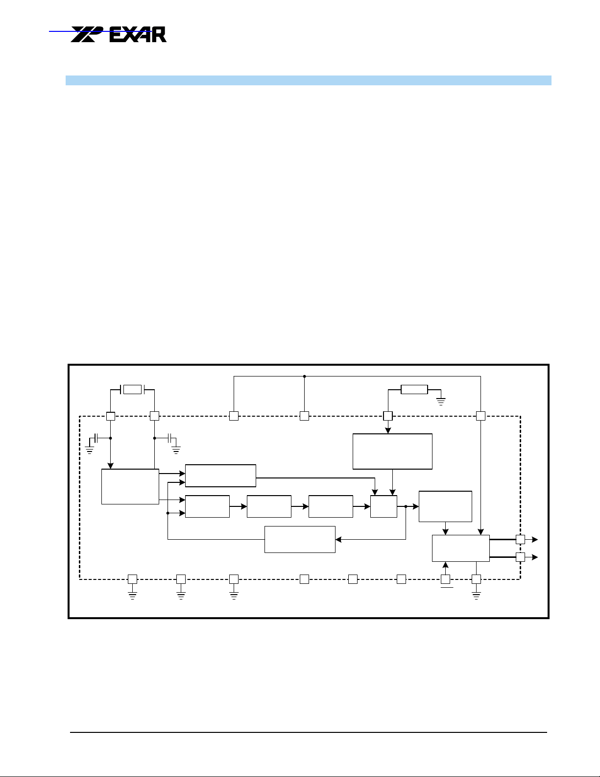
IGURE 1. BLOCK DIAGRAM OF THE XRT8020
F
15-40 MHz
Crystal
XTAL1
XTAL2
AV
DD
FEATURES
• 575 MHz to 675 MHz operating range
• Low Output Jitter: 9ps rms typical at 622 MHz
• On Chip Crystal Oscillator Circuit
• Optimized for 15 to 40 MHz crystals
• Uses parallel fundamental mode crystal
• Selectable 8x, 16x or 32x multiplier
• Selectable ÷ 1or÷ 2 LVDS output
• LVDS output meets TIA/EIA 644A Specification
(2001)
• 3.3V ±10% Low power CMOS: 80 mW typical
• -40°C to +85°C operating temperature
• Extremely small 16-lead QFN package
+3.3V
R
AV
DD
EXT
10kΩ
OV
DD
12 - 20 pF
Oscillator
Circuit &
Input Buffer
AGND
(Crystal)
12 - 20 pF
VCO
Calibration Logic
Phase
Detector
AGND
Charge
Pump
Feedback Divider
AGND
XRT8020
÷÷÷÷ 8, 16 or 32
Loop
Filter
Voltage Reference
&
Bias Generator
VCO
FS0
PD
Selectable
÷÷÷÷ 1or÷÷÷÷ 2
Divider
LVDS Output
OE
O
OUTP
OUTN
GNDFS1
Exar Corporation 48720Kato Road, Fremont CA, 94538 • (510) 668-7000 • FAX (510) 668-7017 • www.exar.com
Page 2
XRT8020
650 MHZ C LOCK & CRYSTAL MULTIPLIER WITH LVDS OUTPUTS
REV. 1.0.2
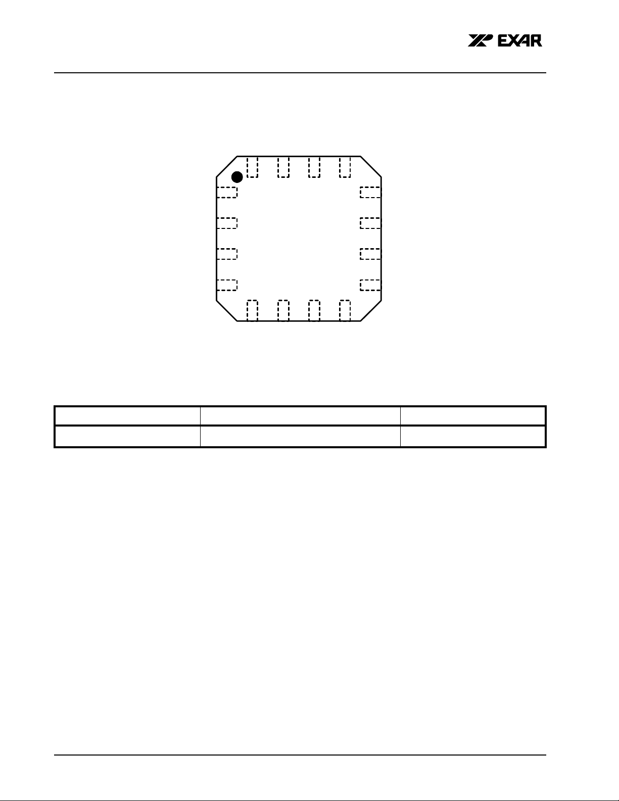
FIGURE 2. XRT8020 PIN LOCATION -(TOP VIEW)
16
1
2
15
14
13
12
11
XRT8020
3
4
5
ORDERING INFORMATION
PART NUMBER PACKAGE OPERATING TEMPERATURE RANGE
XRT8020IL 16 - Pin QFN
6
7
8
10
9
°
Cto+85°C
-40
2
Page 3

XRT8020
650 MHZ CLOCK & CRYSTAL MULTIPLIER WITH LVDS OUTPUTS
REV. 1.0.2
DESCRIPTION .................................................................................................................... 1
APPLICATIONS ......................................................................................................................................... 1
FEATURES ................................................................................................................................................ 1
Figure 1. Block Diagram of the XRT8020 ........................................................................................ 1
ORDERING INFORMATION ............................................................................................................... 2
Figure 2. XRT8020 Pin Location - (Top View) ................................................................................. 2
ABSOLUTE MAXIMUM RATINGS ....................................................................................................................... 3
ELECTRICAL CHARACTERISTICS ..................................................................................................................... 3
Figure 3. LVDS Output Waveforms and Test Circuits .................................................................... 5
1.0 Calibration ................................................................................................................................................. 5
T
ABLE
1: F
ABLE
T
REQUENCYSELECTIONTABLE
2: P
OWER-DOWN ANDOUTPUT TRI-STATE SELECTION TABLE
.............................................................................................. 5
....................................................... 5
2.0 Crystal selection ....................................................................................................................................... 6
3.0 data and plots ........................................................................................................................................... 6
Figure 4. Input Referenced Jitter Connection Diagram ................................................................. 6
Figure 5. Simplified Block Diagram of the XRT8020 and PECL Receiver .................................... 7
Figure 6. LVDS Differential Output ..................................................................................................7
Figure 7. PECL Differential Output ..................................................................................................8
Figure 8. PECL Single-Ended Outputs (Positive and Negative Output Referenced to Ground) 9
ORDERING INFORMATION ............................................................................................. 10
REVISIONS ................................................................................................................................................. 11
I
Page 4
XRT8020
REV. 1.0.2
650 MHZ CLOCK & CRYSTAL MULTIPLIER WITH LVDS OUTPUTS
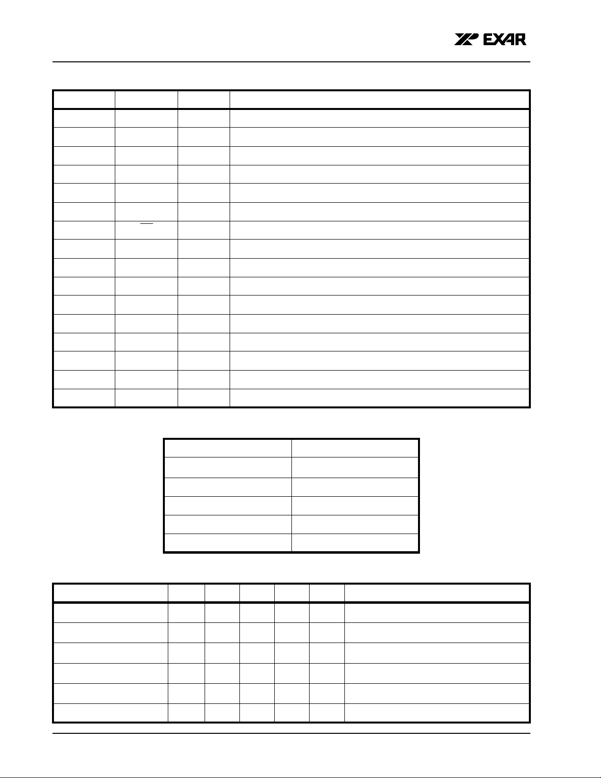
PIN DESCRIPTION
PIN NAME TYPE DESCRIPTION
1 AVDD 3.3V ±10% Analog Supply for Crystal Oscillator
2 AGND Analog Ground for Crystal Oscillator
3 XTAL1 I Crystal pin 1 or external clock input
4 XTAL2 O Crystal pin 2 (output drive for crystal)
5 AGND Analog Ground
6 REXT I External Bias Resistor (10KΩ to ground)
7OE
I Output Enable, Active low (
8 PD I Power Down, Active High
9 FS1 I Frequency select "1"
10 FS0 I Frequency select "0"
Internal 50KΩpull-down to ground
(Internal 50KΩpull-down to ground)
(Internal 50KΩpull-down to ground)
(Internal 50KΩpull-up to VDD)
11 AGND Analog Ground
12 OGND Output Ground for LVDS outputs
13 OUTN O LVDS negative output for 50Ω line
14 OUTP O LVDS positive output for 50Ω line
15 OVDD 3.3V ±10% Digital Supply for LVDS Output buffer
16 AVDD 3.3V ±10% Analog Supply
ABSOLUTE MAXIMUM RATINGS
Supply voltage -0.5 to 6.0 V
V
IN
Storage Temperature -65°C to + 150°C
Operating Temperature -40°C to + 85°C
-0.5 to 6.0 V
)
ESD >2,000 volts
REXT (±1%) 10kΩ
ELECTRICAL CHARACTERISTICS
ARAMETER SYMBOL MIN TYP MAX UNIT CONDITIONS
P
Supply Voltage V
Supply current I
Power Save Current I
Input Digital High V
Input Digital Low V
DD
DD
DD
INH
INL
3.0 3.3 3.6 V
25 30 mA VDD = 3.3V
6 mA VDD=3.3V,PD=1,OEB=0
2.0 V Pins 7, 8, 9, 10
0.8 V Pins 7, 8, 9, 10
Crystal Frequency 15 27 MHz See Section 2.0 for Crystal Selection
3
Page 5
650 MHZ CLOCK & CRYSTAL MULTIPLIER WITH LVDS OUTPUTS
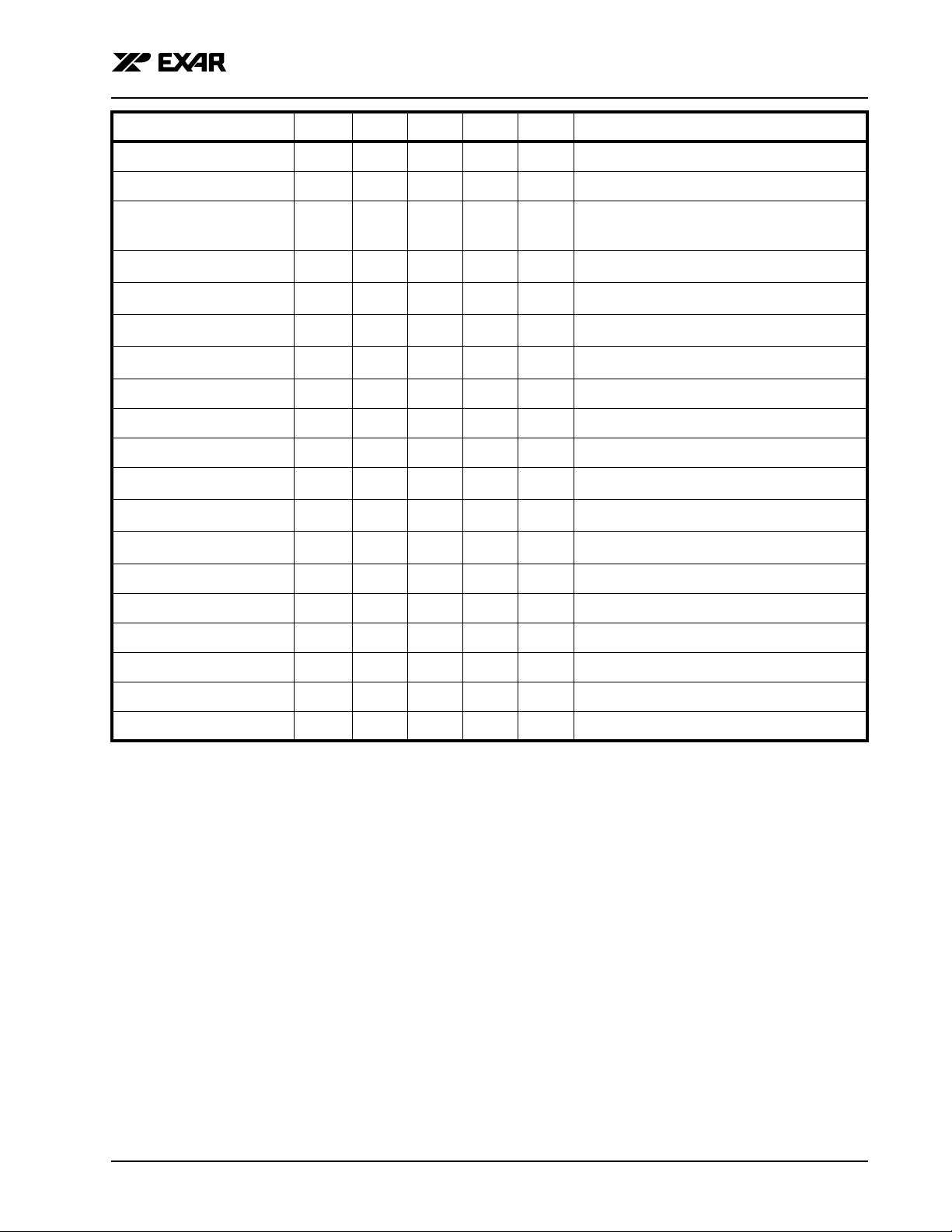
ARAMETER SYMBOL MIN TYP MAX UNIT CONDITIONS
P
Crystal Frequency 27 40 MHz See Section 2.0 for Crystal Selection
Clock Input Frequency 72 85 MHz ACCoupled (FS0=1, FS1=1)
Poweron Calibration time 5 ms After VDD reaches 2.8V
N
OTE
: Calibration time = 16,000 clock cycles
XRT8020
REV. 1.0.2
Max Frequency Out F
Max Frequency Out F
Rise time T
Fall Time T
OUT
OUT
575 675 MHz 624 MHz nominal F
285 340 MHz 312 MHz nominal F
R
F
350 ps CL = 5pF, RL = 100Ω, (20% - 80%)
350 ps CL = 5pF, RL = 100Ω, (20% - 80%)
(See Table 1)
OUT
(See Table 1)
OUT
Duty cycle 45 55 % LVDS output
Differential Output Skew 10 ps See Figure 3
Output Loading 100 Ω
Output Voltage Swing V
Common Mode Voltage V
OUT
CM
Output Short Circuit Current -5.7 -10 mA Current limit to ground, V
250 450 mV Magnitude of (OUTP-OUTN)
1.0 1.2 1.4 V
DD
Cycle-to-Cycle Jitter 3 ps rms, at 624 MHz
Cycle-to-Cycle Jitter 3 ps rms, at 312 MHz
Accumulated Jitter 12 ps rms, at 624 MHz
Accumulated Jitter 12 ps rms, 312 MHz
Input Referenced Jitter 9 ps rms at 622 MHz, See Figure 4
or Vp to Vn
Input Referenced Jitter 9 ps rms at 312 MHz, See Figure 4
4
Page 6
XRT8020
REV. 1.0.2
650 MHZ CLOCK & CRYSTAL MULTIPLIER WITH LVDS OUTPUTS
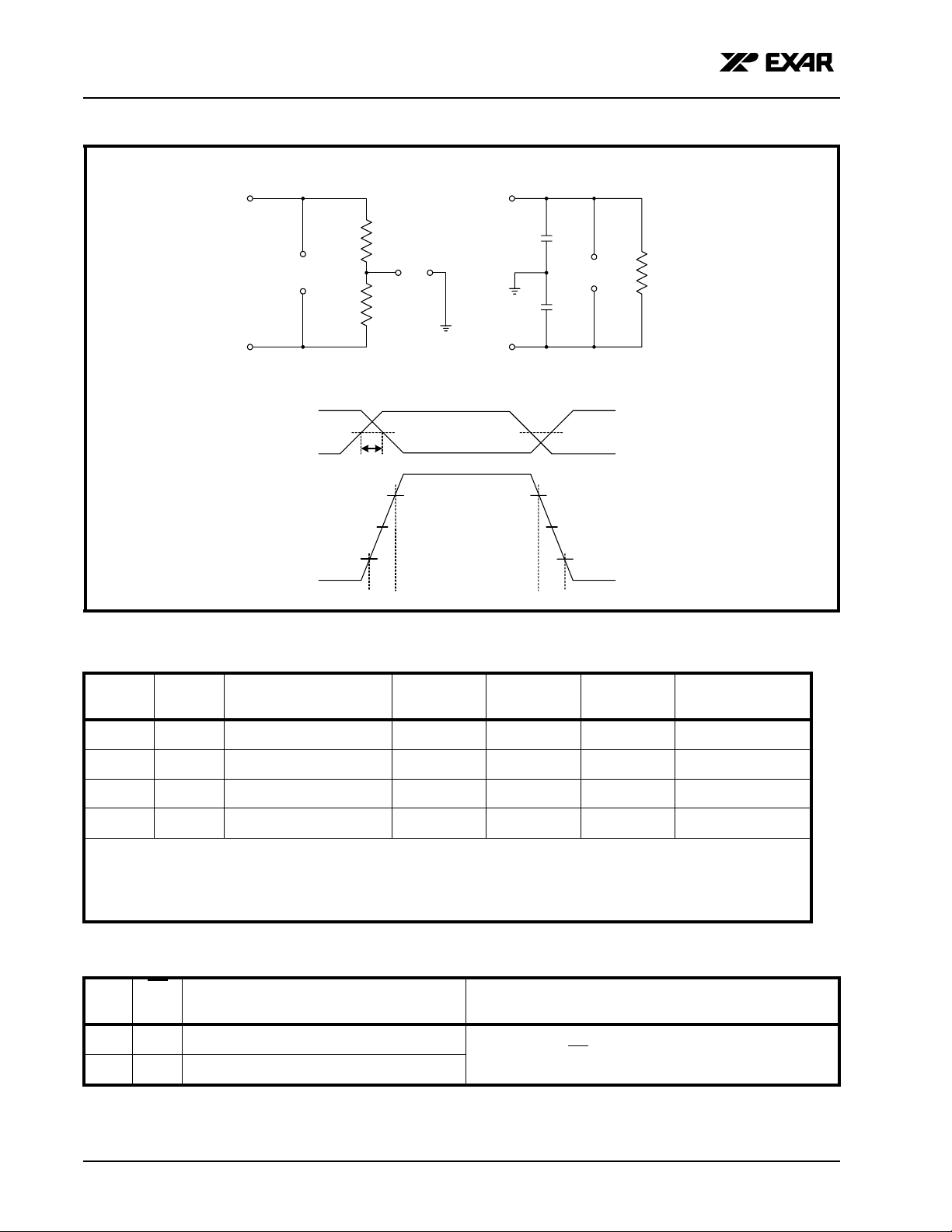
FIGURE 3. LVDS OUTPUT WAVEFORMS AND TEST CIRCUITS
LDVS Levels Test Circuit LDVS Switching Test Circuit
OUTP
OUTN
V
OUTP
OUTN
VOUT
OUTP
50Ω
OUT
50% 50%
0V
20%
V
CM
50Ω
LDVS Transition Time Waveform
VCM (Differential)
t
skew
80%
0V (Differential)
T
R
C
L
CL=5pF
OUTN
=5pF
80%
V
OUT
20%
T
F
R
L
= 100Ω
ABLE 1: FREQUENCY SELECTION TABLE
T
FS0
P
IN 10
FS1
PIN 9
C
RYSTAL OR CLOCK
FREQUENCY
INTERNAL
CAPACITOR
MULTIPLY
RATIO
OUTPUT
DIVIDE
1 1 78.0 MHz Clock NA 8x 1 624 MHz
0 1 39.0 MHz 12 pF 16x 1 624 MHz
1 0 19.5 MHz 20 pF 32x 1 624 MHz
0 0 19.5 MHz 20 pF 32x 2 312 MHz
N
OTES
:
1. Use Parallel Fundamental mode crystal
2. FS0 has an internal 50KΩ pull-up resistor to VDD
3. FS1 has an internal 50K
Ω
pull-down resistor to GND
TABLE 2: POWER-DOWN AND OUTPUT TRI-STATE SELECTION TABLE
IN 8
OE
PIN 7
TATUS
S
1 X Outputs tri-stated and chip Powered-down
0 1 Outputtri-stated
N
OTES
:
1. “X" = Don't care
2. PD and OE have an internal 50KΩpull-down resistor to ground.
PD
P
1.0 CALIBRATION
OUTPUT
FREQUENCY
5
Page 7
XRT8020
650 MHZ CLOCK & CRYSTAL MULTIPLIER WITH LVDS OUTPUTS
REV. 1.0.2
The XRT8020 synthesizer jitter performance is optimized by calibration of its Voltage Controlled Oscillator
(VCO) upon initial power application. This power ON calibration procedure is automatic and completely transparent to the user. It is initiated automatically upon first application of VDD. In order to bring the center frequency of the VCO close to the desired output frequency, the VCO bias current is adjusted via a current DAC
at initial power application. The center frequency of VCO is checked against input reference frequency and calibrated internally to the desired output frequency value. These bias voltage trim bits are then held in latches for
as long as the VDD is held above 2.7V (minimum specified operational value of VDD). The user should note
following important facts about this calibration procedure for proper operation of the XRT8020:
For proper operation of the chip and to achieve lowest jitter, the user should follow layout guidelines as
•
described in the User Guide.
An input crystal of appropriate frequency should be connected at XTAL1 and XTAL2 pins before power is
•
applied to the chip.
All VDD pins should be tied to 3.3V ±10% simultaneously.
•
The power supply should turn on without bouncing below 2.0V smoothly to its specified value in no more
•
than 50msec.
The calibration takes place during VDD ramp up between 2.6V to 3V values. Once the VDD reaches and
•
maintains 3.0V, the chip retains the calibrated VCO bias voltages in internal latches for proper operation.
To change a widely different value of crystal or input reference frequency, it is recommended to power
•
down the chip by bringing VDD to 0V and restarting after the change in frequency has occurred.
2.0 CRYSTAL SELECTION
It is recommended that a Fundamental Mode Crystal be used as the timing reference of the XRT8020. The following part has been qualified by EXAR:
CITIZEN Quartz Crystals
20 MHz : HCM49-20.000MABJT
40 MHz : HCM49-40.000MABJT
3.0 DATA AND PLOTS
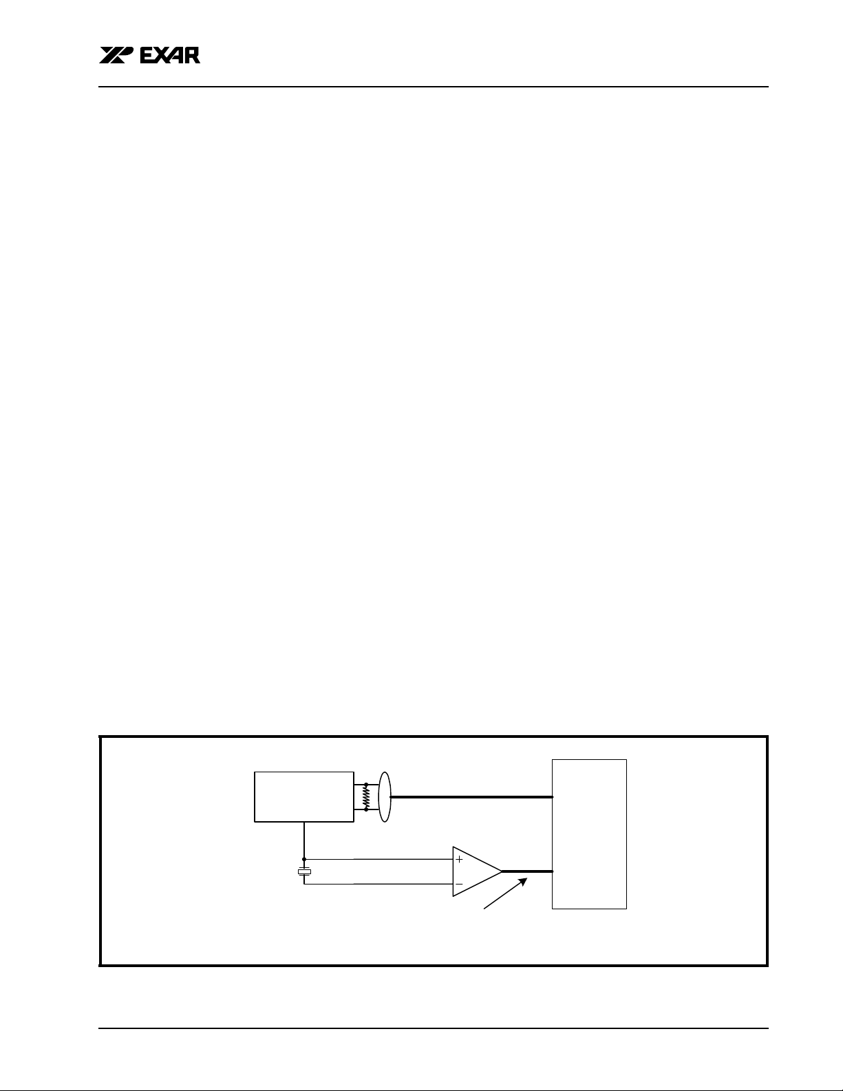
All plots were recorded using the following parameters and test setup:
VDD = 3.3 V
•
2” 100
•
•
•
IGURE 4. INPUT REFERENCED JITTER CONNECTION DIAGRAM
F
Ω Differential Transmission Lines (from LVDS outputs to receiver inputs)
Fundamental Mode Crystal of 20 MHz
Vref = 1.5 V (PECL Receiver)
Outp
XRT8020 Channel 1
Outn
20.0Mhz
Crystal
P6330 Differential Probe
Tektronix
MAX9111ESA
Tektronix
P6245 TDS 500/600
Channel 2
Tektronix
TDS7404
6
Page 8
XRT8020
REV. 1.0.2
650 MHZ CLOCK & CRYSTAL MULTIPLIER WITH LVDS OUTPUTS
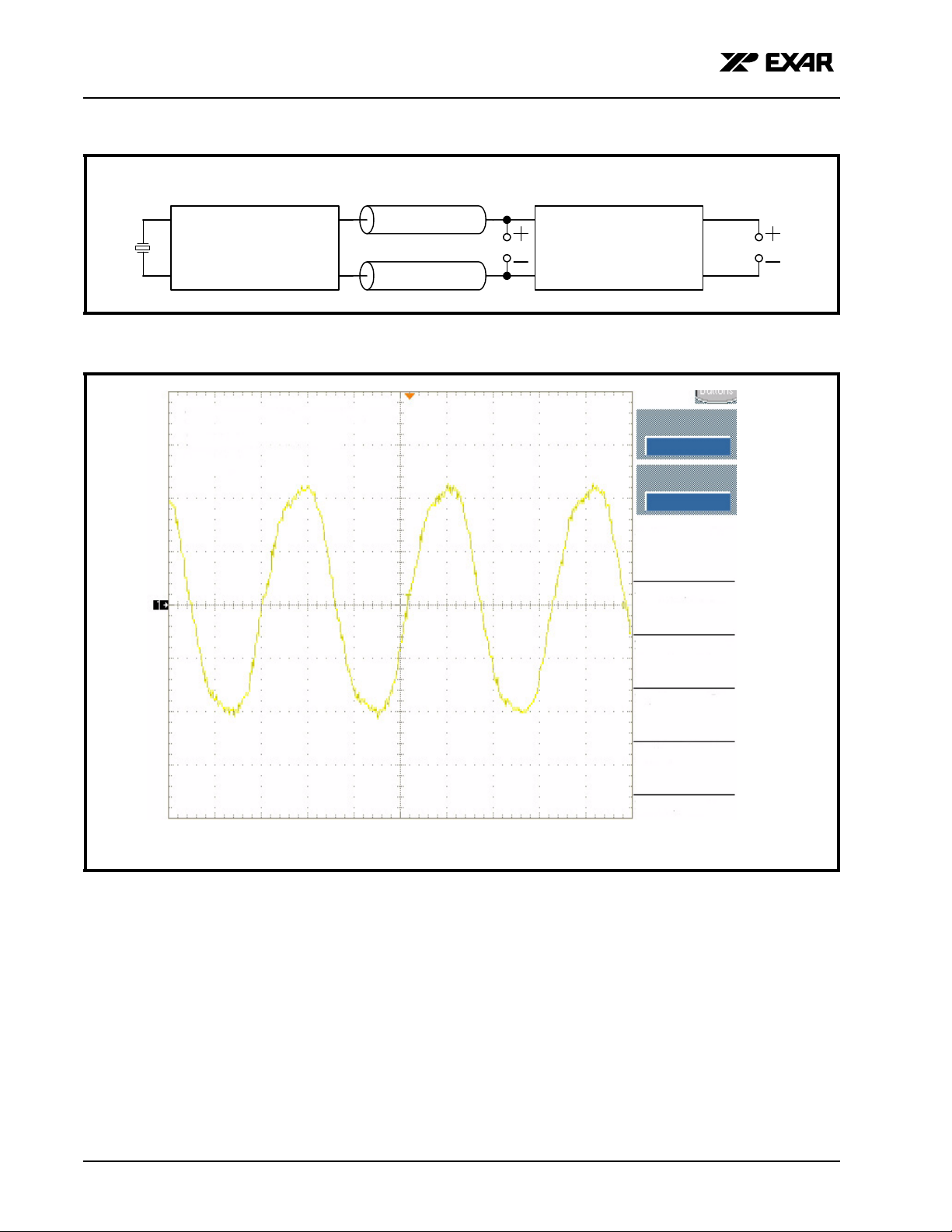
FIGURE 5. SIMPLIFIED BLOCK DIAGRAM OF THE XRT8020 AND PECL RECEIVER
100ohm Transmission Lines
XRT8010/20
Clock Synthesizer
FIGURE 6. LVDS DIFFERENTIAL OUTPUT
LVDS Differential Outputs
LVDS-To-PECL
Receiver
Freq 640.1 MHz
Ampl 824.0 mV
Ch1 200 mV M 500 pS
7
Page 9
650 MHZ CLOCK & CRYSTAL MULTIPLIER WITH LVDS OUTPUTS
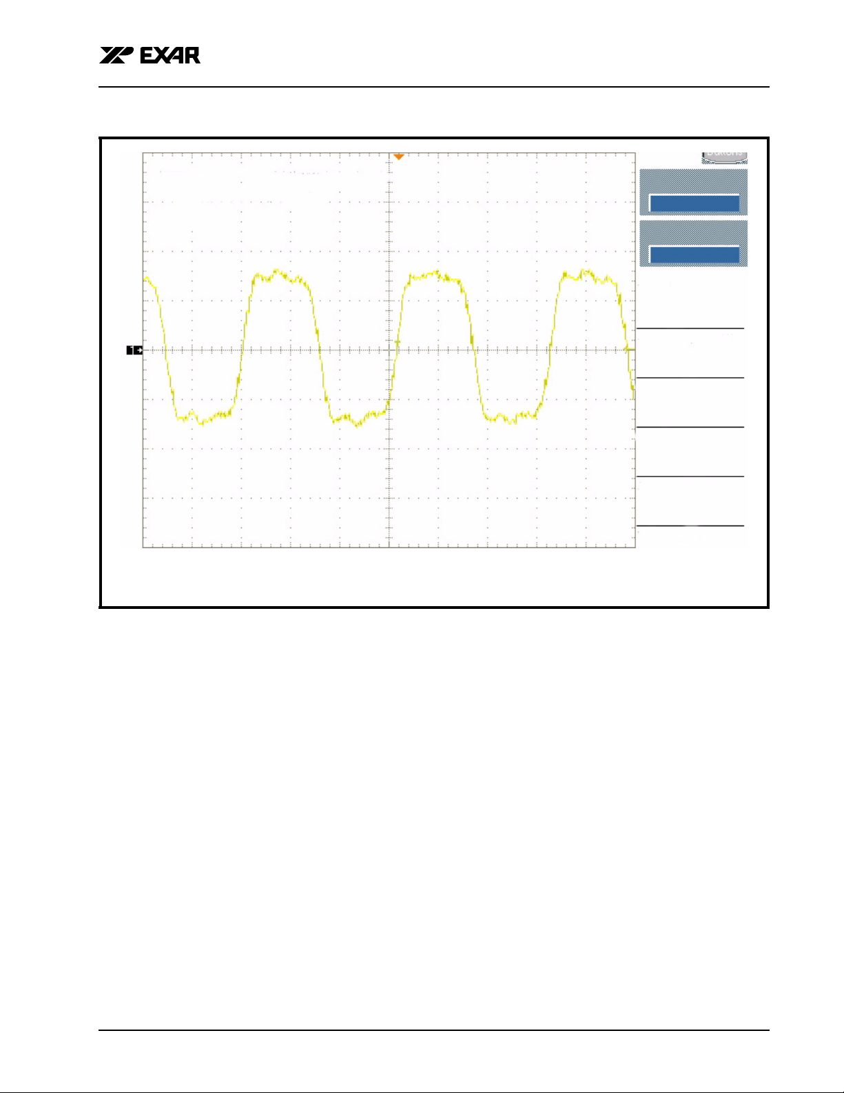
FIGURE 7. PECL DIFFERENTIAL OUTPUT
PECL Differential Outputs
XRT8020
REV. 1.0.2
Freq 640.0 MHz
Ampl 1.42 V
Ch1 500 mV M 500 pS
8
Page 10
XRT8020
REV. 1.0.2
650 MHZ CLOCK & CRYSTAL MULTIPLIER WITH LVDS OUTPUTS
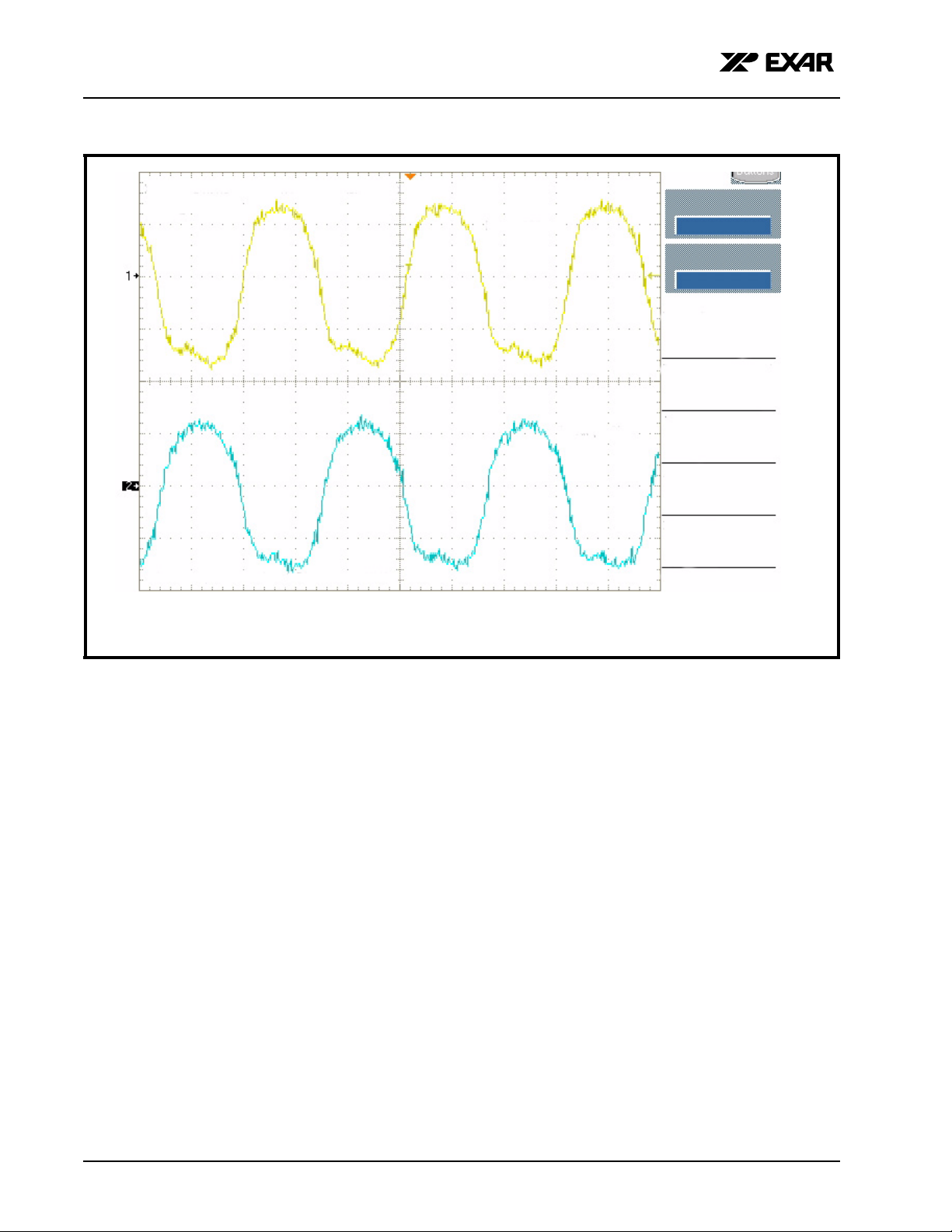
FIGURE 8. PECL SINGLE-ENDED OUTPUTS (POSITIVE AND NEGATIVE OUTPUT REFERENCED TO GROUND)
PECL Single-Ended Outputs
POS Output
Freq(1) 640.3 MHz
Freq(2) 639.9 MHz
Ampl(1) 520.0 mV
Ampl(2) 528.0 mV
Ch1 200 mV M 500 pS
Ch2 200mV
NEG Output
9
Page 11
ORDERING INFORMATION
PART NUMBER PACKAGE OPERATING TEMPERATURE RANGE
XRT8020IL
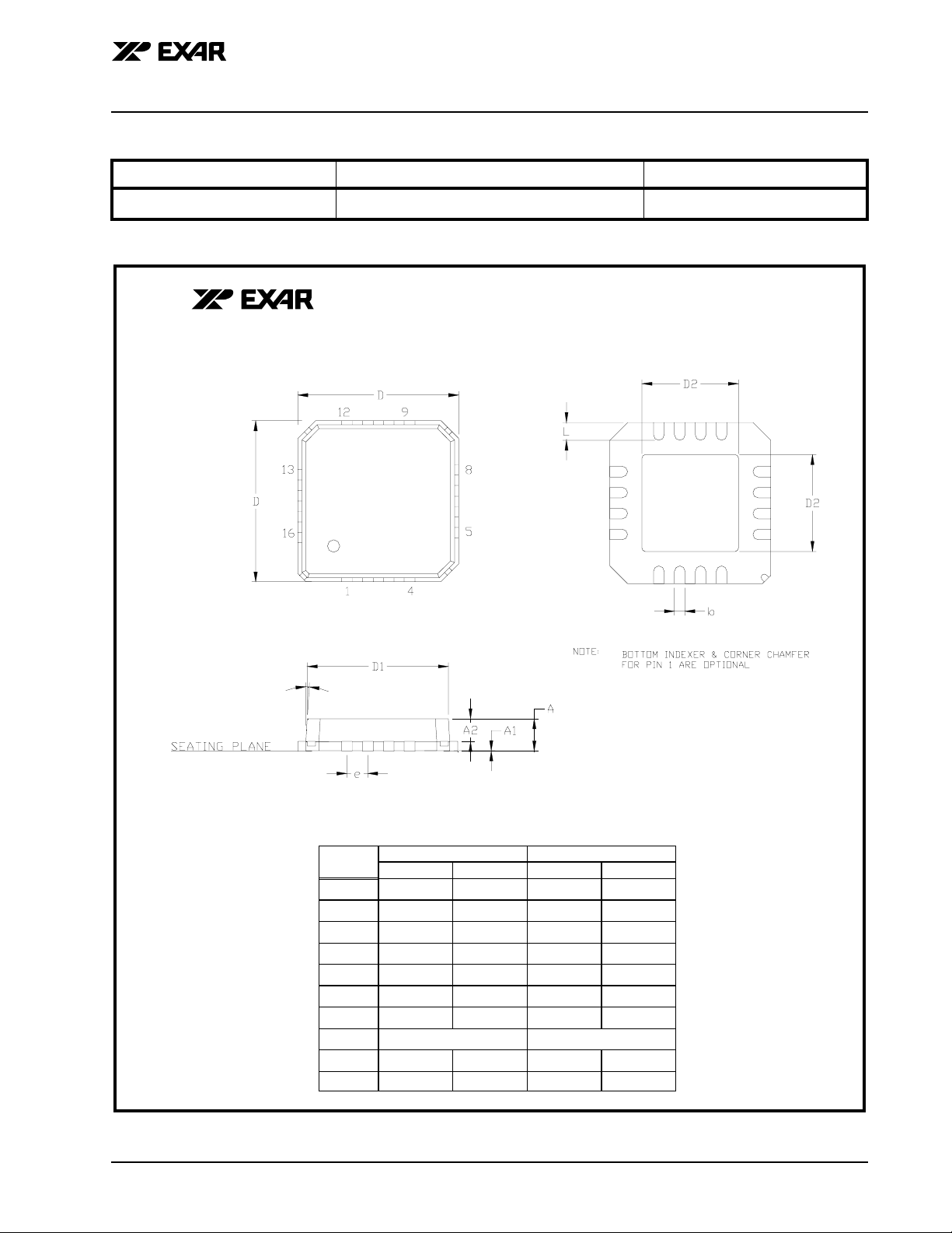
PACKAGE DIMENSIONS
XRT8020
650 MHZ CLOCK & CRYSTAL MULTIPLIER WITH LVDS OUTPUTS
REV. 1.0.2
16-Lead QFN
16 LEAD QUAD FLAT NO LEAD
(4 mm x 4 mm, 0.65 pitch QFN)
Rev. 1.01
°
-40
Cto+85°C
θ
Note: The control dimension is in millimeter.
SYMBOL
A 0.031 0.039 0.80 1.00
A1 0.000 0.002 0.00 0.05
A2 0.000 0.039 0.00 1.00
D 0.154 0.161 3.90 4.10
D1 0.144 0.152 3.65 3.85
D2 0.088 0.100 2.24 2.54
b 0.009 0.015 0.23 0.38
e 0.0256 BSC 0.65 BSC
L 0.014 0.030 0.35 0.75
θ
INCHES MILLIMETERS
MIN MAX MIN MAX
0° 12° 0° 12°
Note: the actual center pad
ismetallicandthesize(D2)
is device-dependent w/ a
typical tolerance of 0.3mm
10
Page 12

XRT8020
650 MHZ CLOCK & CRYSTAL MULTIPLIER WITH LVDS OUTPUTS
REV. 1.0.2
REVISIONS
P1.0.1 Accumulated output jitter in electrical specs changed from 25 ps @ 624MHz to 20 @ 622Mhz and
TBD to 20 ps @312Mhz. Pin 9 has internal a pull-down resistor instead of pull-up. Table 1 FS0 and FS1 bit
pattern changed.
P1.0.2 Changed typical jitter to 6ps and changed package to QFN
P1.0.3 Corrected package dimension dimension "e" to 0.65 mm BSC. Updated electrical tables. Added de-
scriptive sections on Calibration, Crystal Selection and Data and Plots.
1.0.0 Final Release. Added intrinsic jitter measurements to the electrical characteristics.
1.0.1 Changed the page numbering. Changed the QLP to QFN in the Features on page 1.
1.0.2 Changed the Package Drawing and Dimensions.
NOTICE
EXAR Corporation reserves the right to make changes to the products contained in this publication in order
to improve design, performance or reliability. EXAR Corporation assumes no responsibility for the use of
any circuits described herein, conveys no license under any patent or other right, and makes no representation that the circuits are free of patent infringement. Charts and schedules contained here in are only for
illustration purposes and may vary depending upon a user’s specific application. While the information in
this publication has been carefully checked; no responsibility, however, is assumed for inaccuracies.
EXAR Corporation does not recommend the use of any of its products in life support applications where
the failure or malfunction of the product can reasonably be expected to cause failure of the life support system or to significantly affect its safety or effectiveness. Products are not authorized for use in such applications unless EXAR Corporation receives, in writing, assurances to its satisfaction that: (a) the risk of injury
or damage has been minimized; (b) the user assumes all such risks; (c) potential liability of EXAR Corporation is adequately protected under the circumstances.
Copyright 2003 EXAR Corporation
Datasheet November 2003.
Reproduction, in part or whole, without the prior written consent of EXAR Corporation is prohibited.
11
 Loading...