

现货库存、技术资料、百科信息、热点资讯,精彩尽在鼎好!
HIGH-VOLTAGE HIGH-CURRENT DARLINGTON TRANSISTOR ARRAYS
D
500-mA Rated Collector Current
(Single Output)
D
High-Voltage Outputs . . . 50 V
D
Output Clamp Diodes
D
Inputs Compatible With Various Types of
Logic
D
Relay Driver Applications
D
Designed to Be Interchangeable With
Sprague ULN2001A Series
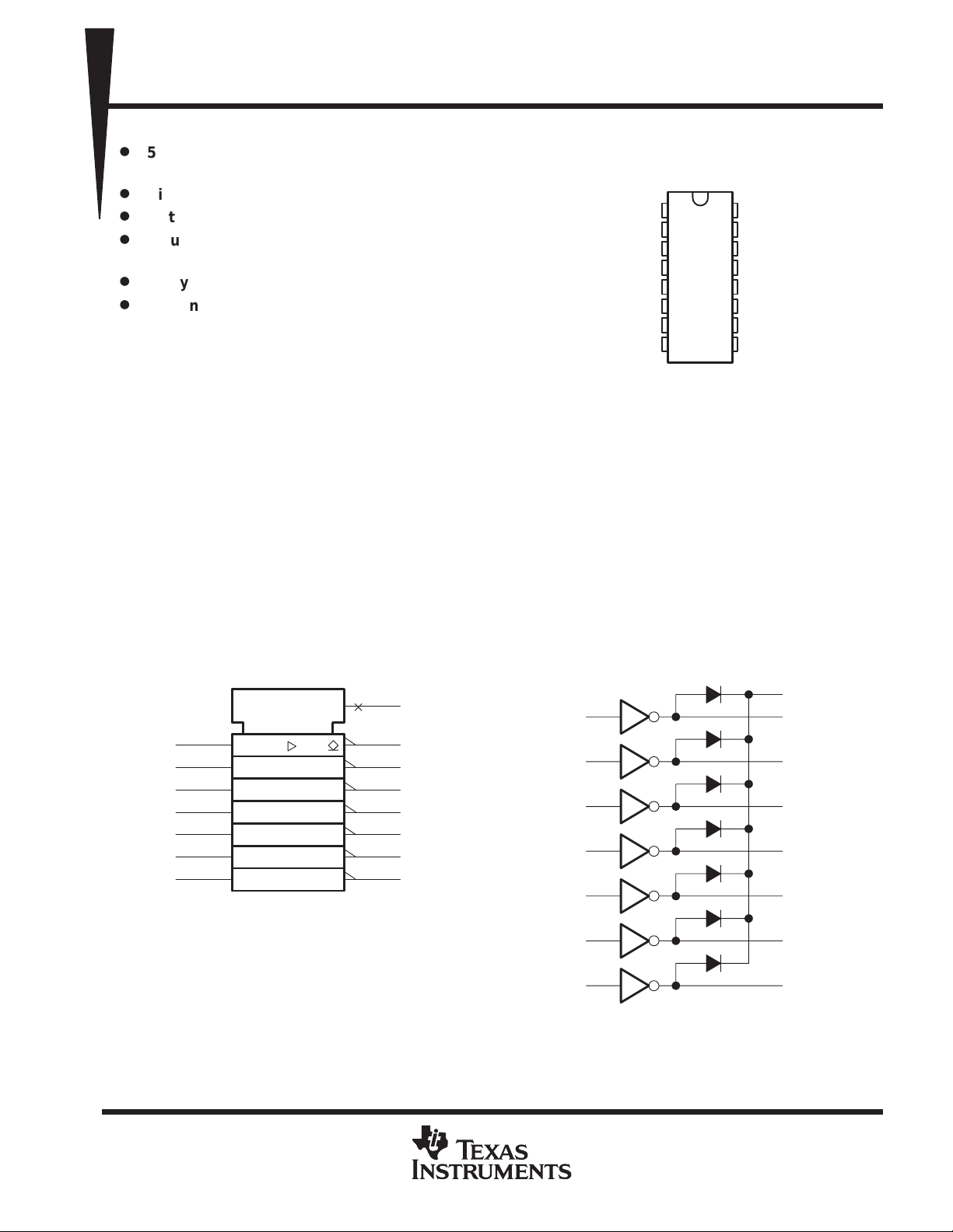
description
The ULN2001A, ULN2002A, ULN2003A, and ULN2004A are monolithic high-voltage, high-current Darlington
transistor arrays. Each consists of seven npn Darlington pairs that feature high-voltage outputs with
common-cathode clamp diodes for switching inductive loads. The collector-current rating of a single Darlington
pair is 500 mA. The Darlington pairs may be paralleled for higher current capability . Applications include relay
drivers, hammer drivers, lamp drivers, display drivers (LED and gas discharge), line drivers, and logic buffers.
For 100-V (otherwise interchangeable) versions, see the SN75465 through SN75469.
ULN2001A, ULN2002A, ULN2003A, ULN2004A
DARLINGTON TRANSISTOR ARRAYS
SLRS027 – DECEMBER 1976 – REVISED APRIL 1993
D OR N PACKAGE
(TOP VIEW)
16
1B
2B
3B
4B
5B
6B
7B
1
2
3
4
5
6
7
8
E
15
14
13
12
11
10
1C
2C
3C
4C
5C
6C
7C
9
COM
The ULN2001A is a general-purpose array and can be used with TTL and CMOS technologies. The ULN2002A
is specifically designed for use with 14- to 25-V PMOS devices. Each input of this device has a zener diode and
resistor in series to control the input current to a safe limit. The ULN2003A has a 2.7-kΩ series base resistor
for each Darlington pair for operation directly with TTL or 5-V CMOS devices. The ULN2004A has a 10.5-kΩ
series base resistor to allow its operation directly from CMOS devices that use supply voltages of 6 to 15 V . The
required input current of the ULN2004A is below that of the ULN2003A, and the required voltage is less than
that required by the ULN2002A.
logic symbol
1B
2B
3B
4B
5B
6B
7B
†
This symbol is in accordance with ANSI/IEEE Std 91-1984
and IEC Publication 617-12.
†
9
16
15
14
13
12
10
COM
1C
2C
3C
4C
5C
11
6C
7C
CLAMP
1
2
3
4
5
6
7
logic diagram
1
1B
2
2B
3
3B
4
4B
5
5B
6
6B
16
15
14
13
12
9
COM
1C
2C
3C
4C
5C
11
6C
PRODUCTION DATA information is current as of publication date.
Products conform to specifications per the terms of Texas Instruments
standard warranty. Production processing does not necessarily include
testing of all parameters.
7
7B
POST OFFICE BOX 655303 • DALLAS, TEXAS 75265
10
7C
Copyright 1993, Texas Instruments Incorporated
1
ULN2001A, ULN2002A, ULN2003A, ULN2004A
PACKAGE
A
DARLINGTON TRANSISTOR ARRAYS
SLRS027 – DECEMBER 1976 – REVISED APRIL 1993
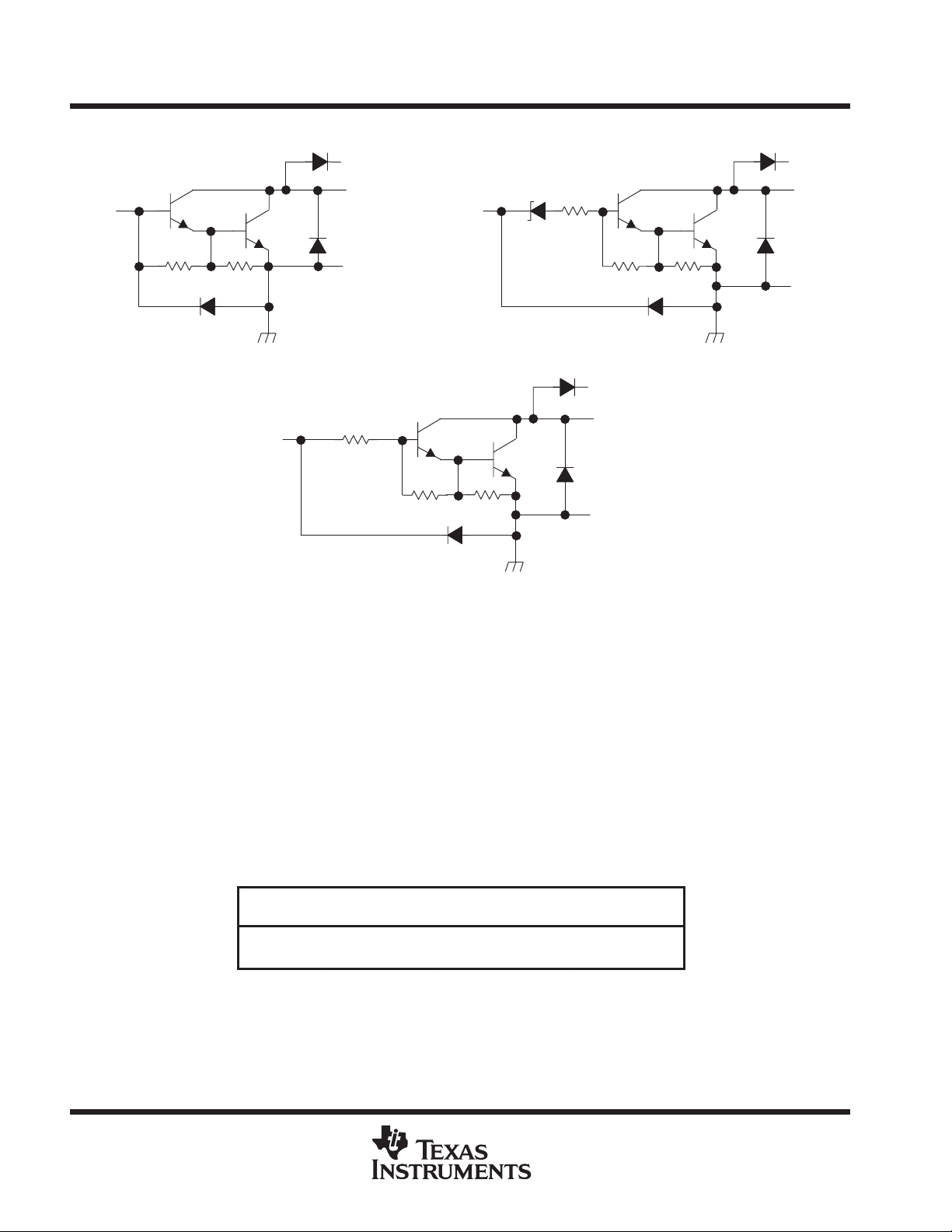
schematics (each Darlington pair)
Input B
7.2 kΩ 3 kΩ
ULN2001A
Input B
ULN2003A: RB = 2.7 kΩ
ULN2004A: RB = 10.5 kΩ
All resistor values shown are nominal.
COM
Output C
E
R
B
Input B
7.2 kΩ
3 kΩ
ULN2003A, ULN2004A
7 V
10.5 kΩ
Output C
7.2 kΩ
COM
E
3 kΩ
ULN2002A
COM
Output C
E
absolute maximum ratings at 25°C free-air temperature (unless otherwise noted)
Collector-emitter voltage 50 V. . . . . . . . . . . . . . . . . . . . . . . . . . . . . . . . . . . . . . . . . . . . . . . . . . . . . . . . . . . . . . . . . . . .
Input voltage, VI (see Note 1) 30 V. . . . . . . . . . . . . . . . . . . . . . . . . . . . . . . . . . . . . . . . . . . . . . . . . . . . . . . . . . . . . . . .
Peak collector current (see Figures 14 and 15) 500 mA. . . . . . . . . . . . . . . . . . . . . . . . . . . . . . . . . . . . . . . . . . . . .
Output clamp current, IOK 500 mA. . . . . . . . . . . . . . . . . . . . . . . . . . . . . . . . . . . . . . . . . . . . . . . . . . . . . . . . . . . . . . . .
Total emitter-terminal current –2.5 A. . . . . . . . . . . . . . . . . . . . . . . . . . . . . . . . . . . . . . . . . . . . . . . . . . . . . . . . . . . . . .
Continuous total power dissipation See Dissipation Rating Table. . . . . . . . . . . . . . . . . . . . . . . . . . . . . . . . . . . . .
Operating free-air temperature range, T
Storage temperature range, T
–65°C to 150°C. . . . . . . . . . . . . . . . . . . . . . . . . . . . . . . . . . . . . . . . . . . . . . . . . . .
stg
Lead temperature 1,6 mm (1/16 inch) from case for 10 seconds 260°C. . . . . . . . . . . . . . . . . . . . . . . . . . . . . . .
NOTE 1: All voltage values are with respect to the emitter/substrate terminal E, unless otherwise noted.
POWER RATING ABOVE TA = 25°CAPOWER RATING
D 950 mW 7.6 mW/°C 494 mW
N 1150 mW 9.2 mW/°C 598 mW
–20°C to 85°C. . . . . . . . . . . . . . . . . . . . . . . . . . . . . . . . . . . . . . . . . . . .
A
DISSIPATION RATING TABLE
T
= 25°C DERATING FACTOR T
= 85°C
2
POST OFFICE BOX 655303 • DALLAS, TEXAS 75265
PARAMETER
TEST CONDITIONS
UNIT
()
saturation voltage
2
CE
,
I
Off-state input current
3
CE
,
C
µ
506550
65µA
IRClamp reverse current
7
A
PARAMETER
TEST CONDITIONS
UNIT
V
On-state input voltage
6
V
V
V
()
saturation voltage
2
CE
,
I
Off-state input current
3
CE
,
C
µ ,
506550
65µA
IRClamp reverse current
7
A
ULN2001A, ULN2002A, ULN2003A, ULN2004A
DARLINGTON TRANSISTOR ARRAYS
electrical characteristics, TA = 25°C (unless otherwise noted)
TEST
V
I(on)
V
CE(sat)
V
F
I
CEX
I(off)
I
I
h
FE
C
i
FIGURE
On-state input voltage 6 VCE = 2 V, IC = 300 mA 13 V
Collector-emitter
Clamp forward voltage 8 IF = 350 mA 1.7 2 1.7 2 V
Collector cutoff current
p
Input current 4 VI = 17 V 0.82 1.25 mA
p
Static forward current
transfer ratio
Input capacitance VI = 0, f = 1 MHz 15 25 15 25 pF
II = 250 µA, IC = 100 mA 0.9 1.1 0.9 1.1
5
II = 350 µA, IC = 200 mA 1 1.3 1 1.3
II = 500 µA, IC = 350 mA 1.2 1.6 1.2 1.6
1 VCE = 50 V, II = 0 50 50
V
= 50 V,
TA = 70°C
V
= 50 V,
TA = 70°C
VR = 50 V, TA = 70°C 100 100
VR = 50 V 50 50
5 VCE = 2 V, IC = 350 mA 1000
II = 0 100 100
VI = 6 V 500
IC = 500 µA,
MIN TYP MAX MIN TYP MAX
SLRS027 – DECEMBER 1976 – REVISED APRIL 1993
ULN2001A ULN2002A
V
µA
µ
electrical characteristics, TA = 25°C (unless otherwise noted)
TEST
I(on)
V
CE(sat)
I
CEX
V
F
I(off)
I
I
C
i
FIGURE
IC = 125 mA 5
IC = 200 mA 2.4 6
p
Collector-emitter
Collector cutoff current
Clamp forward voltage 8 IF = 350 mA 1.7 2 1.7 2 V
p
Input current 4
p
Input capacitance VI = 0, f = 1 MHz 15 25 15 25 pF
5
1 VCE = 50 V, II = 0 50 50
= 2
CE
II = 250 µA, IC = 100 mA 0.9 1.1 0.9 1.1
II = 350 µA, IC = 200 mA 1 1.3 1 1.3
II = 500 µA, IC = 350 mA 1.2 1.6 1.2 1.6
V
= 50 V,
TA = 70°C
V
= 50 V, I
TA = 70°C
VI = 3.85 V 0.93 1.35
VI = 5 V 0.35 0.5
VI = 12 V 1 1.45
VR = 50 V 50 50
VR = 50 V, TA = 70°C 100 100
IC = 250 mA 2.7
IC = 275 mA 7
IC = 300 mA 3
IC = 350 mA 8
II = 0 100 100
VI = 1 V 500
= 500 µA,
MIN TYP MAX MIN TYP MAX
ULN2003A ULN2004A
V
µA
mA
µ
POST OFFICE BOX 655303 • DALLAS, TEXAS 75265
3
ULN2001A, ULN2002A, ULN2003A, ULN2004A
See Figure 9
)
DARLINGTON TRANSISTOR ARRAYS
SLRS027 – DECEMBER 1976 – REVISED APRIL 1993
switching characteristics, TA = 25°C
PARAMETER TEST CONDITIONS MIN TYP MAX UNIT
t
Propagation delay time, low-to-high-level output
PLH
t
Propagation delay time, high-to-low-level output
PHL
V
High-level output voltage after switching
OH
PARAMETER MEASUREMENT INFORMATION
VS = 50 V,
See Figure 10
IO ≈ 300 mA,
0.25 1 µs
0.25 1 µs
VS–20 mV
Open
Open
Figure 1. I
I
I(off)
Figure 3. I
I
I
Test Circuit
CEX
Test Circuit
I(off)
Open
V
Open
CE
I
CEX
hFE =
V
CE
V
I
Figure 2. I
V
CE
I
C
I
I(on)
V
I
Figure 4. I
I
C
I
I
I
C
V
I(on)
Open
Test Circuit
CEX
Open
Test Circuit
I
Open
V
CE
I
CEX
Open
V
CE
I
C
NOTE: II is fixed for measuring V
measuring hFE.
Figure 5. hFE, V
4
CE(sat
, variable for
CE(sat)
Test Circuit
POST OFFICE BOX 655303 • DALLAS, TEXAS 75265
Figure 6. V
Test Circuit
I(on)

ULN2001A, ULN2002A, ULN2003A, ULN2004A
DARLINGTON TRANSISTOR ARRAYS
SLRS027 – DECEMBER 1976 – REVISED APRIL 1993
PARAMETER MEASUREMENT INFORMATION
V
R
I
R
V
Open
F
Open
I
F
Figure 7. I
Output
Generator
(see Note A)
Test Circuit
R
Input
Pulse
Figure 8. VF Test Circuit
50% 50%
t
PHL
50% 50%
VOLTAGE WAVEFORMS
t
PLH
Figure 9. Propagation Delay Time Waveforms
Input
ULN2001A only
2.7 kΩ
ULN2002A
ULN2003A
ULN2004A
Open
1N3064
V
S
2 mH
200 Ω
Output
CL = 15 pF
(see Note B)
TEST CIRCUIT
≤ 5 ns
Input
10% 10%
Output
NOTES: A. The pulse generator has the following characteristics: PRR = 12.5 kHz, ZO = 50 Ω.
B. CL includes probe and jig capacitance.
C. For testing the ULN2001A and the ULN2003A, VIH = 3 V; for the ULN2002A, VIH = 13 V;
for the ULN2004A, VIH = 8 V.
90% 90%
1.5 V 1.5 V
40 µs
VOLTAGE WAVEFORMS
≤ 10 ns
Figure 10. Latch-Up Test Circuit and Voltage Waveforms
POST OFFICE BOX 655303 • DALLAS, TEXAS 75265
V
IH
(see Note C)
0 V
V
OH
V
OL
5

ULN2001A, ULN2002A, ULN2003A, ULN2004A
DARLINGTON TRANSISTOR ARRAYS
SLRS027 – DECEMBER 1976 – REVISED APRIL 1993
TYPICAL CHARACTERISTICS
2.5
2
1.5
1
0.5
0
CE(sat)
0
V
VCE(sat) – Collector-Emitter Saturation Voltage – V
COLLECTOR-EMITTER
SATURATION VOLTAGE
vs
COLLECTOR CURRENT
(ONE DARLINGTON)
TA = 25°C
II = 250 µA
II = 350 µA
II = 500 µA
100 200 300 400 500 600 700
IC – Collector Current – mA
Figure 11
800
2.5
1.5
0.5
CE(sat)
VCE(sat) – Collector-Emitter Saturation Voltage – VV
COLLECTOR-EMITTER
SATURATION VOLTAGE
vs
TOTAL COLLECTOR CURRENT
(TWO DARLINGTONS PARALLELED)
TA = 25°C
2
II = 350 µA
1
0
0
I
– Total Collector Current – mA
C(tot)
Figure 12
II = 250 µA
II = 500 µA
800
700600500400300200100
COLLECTOR CURRENT
INPUT CURRENT
500
RL = 10 Ω
450
TA = 25°C
400
350
300
250
200
150
C
IC – Collector Current – mA
I
100
50
0
0
VS = 10 V
25 50 75 100 125 150 175
II – Input Current – µA
Figure 13
vs
VS = 8 V
200
6
POST OFFICE BOX 655303 • DALLAS, TEXAS 75265
ULN2001A, ULN2002A, ULN2003A, ULN2004A
DARLINGTON TRANSISTOR ARRAYS
SLRS027 – DECEMBER 1976 – REVISED APRIL 1993
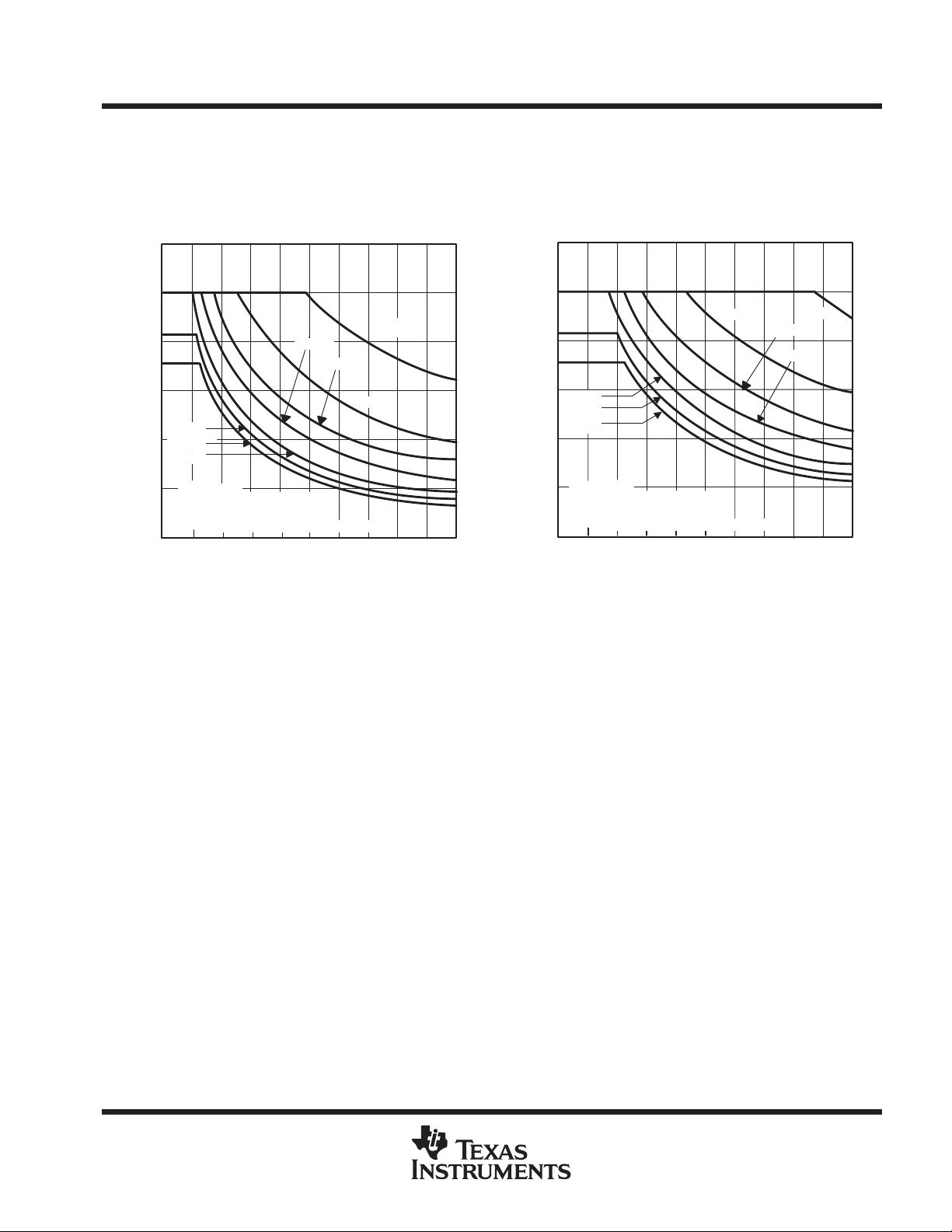
THERMAL INFORMATION
D PACKAGE
MAXIMUM COLLECTOR CURRENT
vs
DUTY CYCLE
600
500
400
300
N = 6
200
N = 7
N = 5
100
C
IC – Maximum Collector Current – mA
I
TA = 70°C
N = Number of Outputs
0
Conducting Simultaneously
10 20 30 40 50 60 70 80 90
0
N = 4
N = 3
Duty Cycle – %
Figure 14
N = 2
N = 1
100
N PACKAGE
MAXIMUM COLLECTOR CURRENT
vs
DUTY CYCLE
600
500
N = 2
400
300
N = 5
N = 6
N = 7
200
100
C
IC – Maximum Collector Current – mA
I
TA = 85°C
N = Number of Outputs
0
Conducting Simultaneously
0
Duty Cycle – %
Figure 15
N = 3
N = 4
N = 1
908070605040302010
100
POST OFFICE BOX 655303 • DALLAS, TEXAS 75265
7

ULN2001A, ULN2002A, ULN2003A, ULN2004A
DARLINGTON TRANSISTOR ARRAYS
SLRS027 – DECEMBER 1976 – REVISED APRIL 1993
APPLICATION INFORMATION
P-MOS
Output
V
DD
V
SS
1
2
3
4
5
6
7
8
ULN2002A
Figure 16. P-MOS to Load
ULN2004A
16
15
14
13
12
11
10
ULN2003A
V
16
15
14
13
12
11
10
9
Lamp
Test
TTL
Output
V
CC
1
2
3
4
5
6
7
8
V
9
Figure 17. TTL to Load
V
V
CC
ULN2003A
V
1
2
3
4
5
6
7
8
CMOS
Output
16
15
14
13
12
11
10
Figure 18. Buffer for Higher Current Loads
1
2
3
R
P
4
5
6
7
9
TTL
Output
8
16
15
14
13
12
11
10
9
Figure 19. Use of Pullup Resistors to
Increase Drive Current
8
POST OFFICE BOX 655303 • DALLAS, TEXAS 75265

IMPORTANT NOTICE
T exas Instruments and its subsidiaries (TI) reserve the right to make changes to their products or to discontinue
any product or service without notice, and advise customers to obtain the latest version of relevant information
to verify, before placing orders, that information being relied on is current and complete. All products are sold
subject to the terms and conditions of sale supplied at the time of order acknowledgement, including those
pertaining to warranty, patent infringement, and limitation of liability.
TI warrants performance of its semiconductor products to the specifications applicable at the time of sale in
accordance with TI’s standard warranty. Testing and other quality control techniques are utilized to the extent
TI deems necessary to support this warranty . Specific testing of all parameters of each device is not necessarily
performed, except those mandated by government requirements.
CERTAIN APPLICATIONS USING SEMICONDUCTOR PRODUCTS MAY INVOLVE POTENTIAL RISKS OF
DEATH, PERSONAL INJURY, OR SEVERE PROPERTY OR ENVIRONMENTAL DAMAGE (“CRITICAL
APPLICATIONS”). TI SEMICONDUCTOR PRODUCTS ARE NOT DESIGNED, AUTHORIZED, OR
WARRANTED TO BE SUITABLE FOR USE IN LIFE-SUPPORT DEVICES OR SYSTEMS OR OTHER
CRITICAL APPLICA TIONS. INCLUSION OF TI PRODUCTS IN SUCH APPLICATIONS IS UNDERST OOD TO
BE FULLY AT THE CUSTOMER’S RISK.
In order to minimize risks associated with the customer’s applications, adequate design and operating
safeguards must be provided by the customer to minimize inherent or procedural hazards.
TI assumes no liability for applications assistance or customer product design. TI does not warrant or represent
that any license, either express or implied, is granted under any patent right, copyright, mask work right, or other
intellectual property right of TI covering or relating to any combination, machine, or process in which such
semiconductor products or services might be or are used. TI’s publication of information regarding any third
party’s products or services does not constitute TI’s approval, warranty or endorsement thereof.
Copyright 1998, Texas Instruments Incorporated
 Loading...