

Page 1
SLUS213 - APRIL 1998
FEATURES
• Complies with SCSI, SCSI-2, SCSI-3
SPI and Ultra SCSI (Fast-20)
• 2.85V Regulated Output Voltage With
1.4% Tolerance
• Provides Current for up to 27 Lines of
Active Termination for SCSI Buses
•−750mA Sourcing Current for
Termination
• +300mA Sinking Current for Active
Negation Drivers
• 0.9V Dropout Voltage Regulator at
750mA and 2.75V Output
• 100µA Supply Current in Disconnect
Mode
• Current Limit and Thermal Shutdown
Protection
• Low Thermal Resistance Surface Mount
Packages
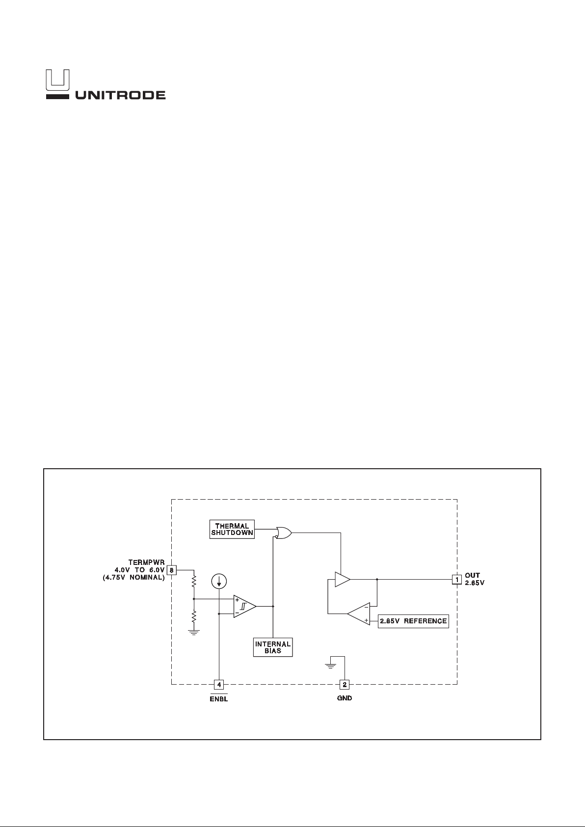
27-Line SCSI Source/Sink Regulator
BLOCK DIAGRAM
UC560
UDG-95136-1
Pin Numbers refer to 8-pin DPpackage.
DESCRIPTION
The UC560 provides current for up to 27 lines of active termination for a
SCSI (Small Computers Systems Interface) parallel bus. The SCSI
standard requires active termination at both ends of the cable. The
UC560 is based on the UC5603 and UC5613 SCSI Active Terminators.
It uses the voltage regulator and internal logic circuits of those parts,
but has no termination circuits.The UC560 provides greater source current drive capability compared to the UC5603 and UC5613.
The UC560 sink current maintains regulation with all active-negation
drivers negated. It provides a disconnect feature which disables the
regulator to greatly reduce standby power. Internal circuit trimming is
utilized for a 1.4% tolerance output voltage. Other features include thermal shutdown and current limit for short circuit conditions.
The UC560 is available in low thermal resistance versions of the industry standard 8-pin power SOIC, 5-pin TO-220 and 5-pin TO-263.
Page 2
2
UC560
ELECTRICAL CHARACTERISTICS
Unless otherwise specified, TA= 0°C to 70°C, TERMPWR = 4.75V, ENBL = 0V,
C
OUT
= 4.7µF, C
TERMPWR
= 4.7µF, TA=TJ.
PARAMETER TEST CONDITIONS MIN TYP MAX UNITS
Supply Current Section
TERMPWR Supply Current No Load 16 22 mA
I
OUT
= –700mA 710 750 mA
Power Down Mode ENBL
= 2.0V 100 140 µA
Regulator Section
Regulator Output Voltage 25°C, No Load 2.81 2.85 2.89 V
Load Regulation I
OUT
= 300mA to –750mA (Note 2) 25 30 mV
Line Regulation TERMPWR = 4.0V to 6.0V, No Load (Note 2) 10 20 mV
Dropout Voltage I
OUT
= –750mA, VOUT = 2.75V 0.9 1.2 V
Short Circuit Current V
OUT
= 0.0V –0.85 –1.3 A
Sinking Current V
OUT
= 3.5V 500 600 mA
ENBL = 2.0V, V
OUT
= 3.0V 1 2 mA
Thermal Shutdown (Note 1) 170 °C
Thermal Shutdown Hysteresis (Note 1) 10 °C
Shutdown Section
ENBL
Threshold 1.1 1.4 1.7 V
Threshold Hysteresis 100 mV
ENBL
Output Current –10 –15 µA
Note 1: Guaranteed by design.Not 100% tested in production.
Note 2: Tested at a constant junction temperature by low duty cycle pulse testing.
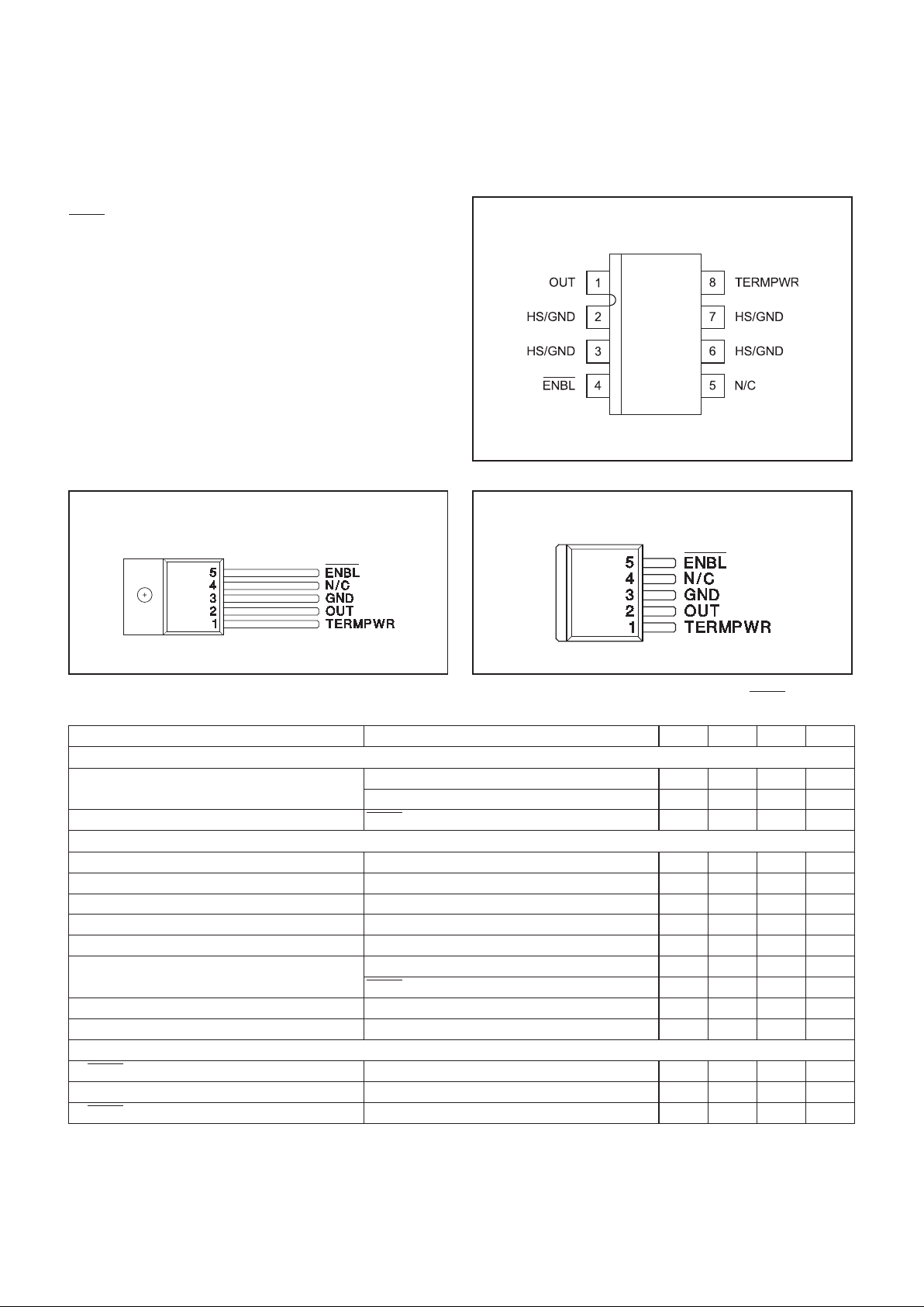
CONNECTION DIAGRAMS
SOIC-8 (Top View)
DP Package
ABSOLUTE MAXIMUM RATINGS
TERMPWR Voltage................................7V
ENBL Voltage ................–0.3V to TERMPWR + 0.3V
Regulator Output Current ..........................1.4A
Power Dissipation ...............................2.5W
Storage Temperature ...................−65°C to +150°C
Junction Temperature...................–55°C to +150°C
Lead Temperature (Soldering, 10 sec.) .............+300°C
Currents are positive into, negative out of the specified terminal. Consult PackagingSection of Databook for thermal limitations and considerations of packages.
RECOMMENDED OPERATING CONDITIONS
TERMPWR Voltage ........................4.0V to 6.0V
ENBL Voltage ........................0VtoTERMPWR
5-Pin TO-220 (Top View)
T Package
5-Pin TO-263 (Top View)
TD Package
Note: TAB is ground.
Note: TAB is ground.
Note: Pins 2,3,6, and 7 are heat sinking pins. Pin 2 is the
connect point for electrical ground.
Page 3

3
UC560
PIN DESCRIPTIONS
ENBL: Enable Bar pin. The ENBL function is active low,
and the pin will source 10µA typically when at ground
and TERMPWR is between 4V and 6V. The part will go
into disable mode if ENBL
is above 1.4V typical, and will
turn back on when ENBL
drops below 1.3V typical. The
part also greatly reduces TERMPWR current when disabled (100µA typical).
GND: Ground pin.
OUT: 2.85V regulated output voltage pin. The part is in-
ternally current limited for both sinking and sourcing cur-
rent to prevent damage. When the part is in disabled
mode (ENBL ≥ 1.4V typical), the output goes to 0V with
no external supply source on OUT.The part will sink current, though, if there is an external supply voltage applied
to OUT when in disabled mode. For best perfomance, a
4.7µF low ESR capacitor is recommended.
TERMPWR: Supply voltage pin. The pin should be de-
coupled with at least a 2.2µF low ESR output capacitor.
For best perfomance, a 4.7µF low ESR capacitor is recommended. Lead lengths should be kept at a minimum.
Figure 2. Typical Wide SCSI Bus Configuration
Utilizing UC560 Device
UDG-96034
Figure 1. Typical SCSI Bus Configuration Utilizing
UC560 Device
APPLICATIONS INFORMATION
UDG-96033
Page 4

4
UC560
UNITRODE CORPORATION
7 CONTINENTAL BLVD.• MERRIMACK, NH 03054
TEL. (603) 424-2410 • FAX (603) 424-3460
2.8
2.81
2.82
2.83
2.84
2.85
2.86
2.87
2.88
2.89
2.9
0
20 40 60 80
TEMPERATURE (°C)
VOUT (V
)
IOUT = -750mA NO LOAD IOUT = 300mA
TYPICAL CHARACTERISTICS
Figure 3. V
OUT
vs Temperature
20
21
22
23
24
25
26
27
28
29
30
0
20 40 60 80
TEMPERATURE (°C)
LOAD REG(mV
)
Figure 5. Load Regulation vs. Temperature
(I
OUT
= 300mA to –750mA)
0.6
0.7
0.8
0.9
1
1.1
1.2
1.3
0
20 40 60 80
TEMPERATURE (°C)
V
IN
-V
OUT
(V)
Figure 4. Dropout Voltage vs. Temperature
(I
OUT
= –750mA, V
OUT
= 2.75V)
-12
-10
-8
-6
-4
-2
0
2
4
0
20 40 60 80
TEMPERATURE (°C)
LINE REG (mV
)
Figure 6. Line Regulation vs Temperature
(TERMPWR = 4.0V to 6.0V)
Page 5

IMPORTANT NOTICE
T exas Instruments and its subsidiaries (TI) reserve the right to make changes to their products or to discontinue
any product or service without notice, and advise customers to obtain the latest version of relevant information
to verify, before placing orders, that information being relied on is current and complete. All products are sold
subject to the terms and conditions of sale supplied at the time of order acknowledgement, including those
pertaining to warranty, patent infringement, and limitation of liability.
TI warrants performance of its semiconductor products to the specifications applicable at the time of sale in
accordance with TI’s standard warranty. Testing and other quality control techniques are utilized to the extent
TI deems necessary to support this warranty. Specific testing of all parameters of each device is not necessarily
performed, except those mandated by government requirements.
CERT AIN APPLICATIONS USING SEMICONDUCTOR PRODUCTS MAY INVOLVE POTENTIAL RISKS OF
DEATH, PERSONAL INJURY, OR SEVERE PROPERTY OR ENVIRONMENTAL DAMAGE (“CRITICAL
APPLICATIONS”). TI SEMICONDUCTOR PRODUCTS ARE NOT DESIGNED, AUTHORIZED, OR
WARRANTED TO BE SUITABLE FOR USE IN LIFE-SUPPORT DEVICES OR SYSTEMS OR OTHER
CRITICAL APPLICATIONS. INCLUSION OF TI PRODUCTS IN SUCH APPLICA TIONS IS UNDERSTOOD T O
BE FULLY AT THE CUSTOMER’S RISK.
In order to minimize risks associated with the customer’s applications, adequate design and operating
safeguards must be provided by the customer to minimize inherent or procedural hazards.
TI assumes no liability for applications assistance or customer product design. TI does not warrant or represent
that any license, either express or implied, is granted under any patent right, copyright, mask work right, or other
intellectual property right of TI covering or relating to any combination, machine, or process in which such
semiconductor products or services might be or are used. TI’s publication of information regarding any third
party’s products or services does not constitute TI’s approval, warranty or endorsement thereof.
Copyright 1999, Texas Instruments Incorporated
 Loading...