

9/94
• Optimized for Off-line and DC to DC
Converters
• Low Start Up Current (<0.5mA)
• Trimmed Oscillator Discharge Current
• Automatic Feed Forward Compensation
• Pulse-by-Pulse Current Limiting
• Enhanced Load Response Characteristics
• Under-Voltage Lockout With Hysteresis
• Double Pulse Suppression
• High Current Totem Pole Output
• Internally Trimmed Bandgap Reference
• 500kHz Operation
• Low R
O Error Amp
Current Mode PWM Controller
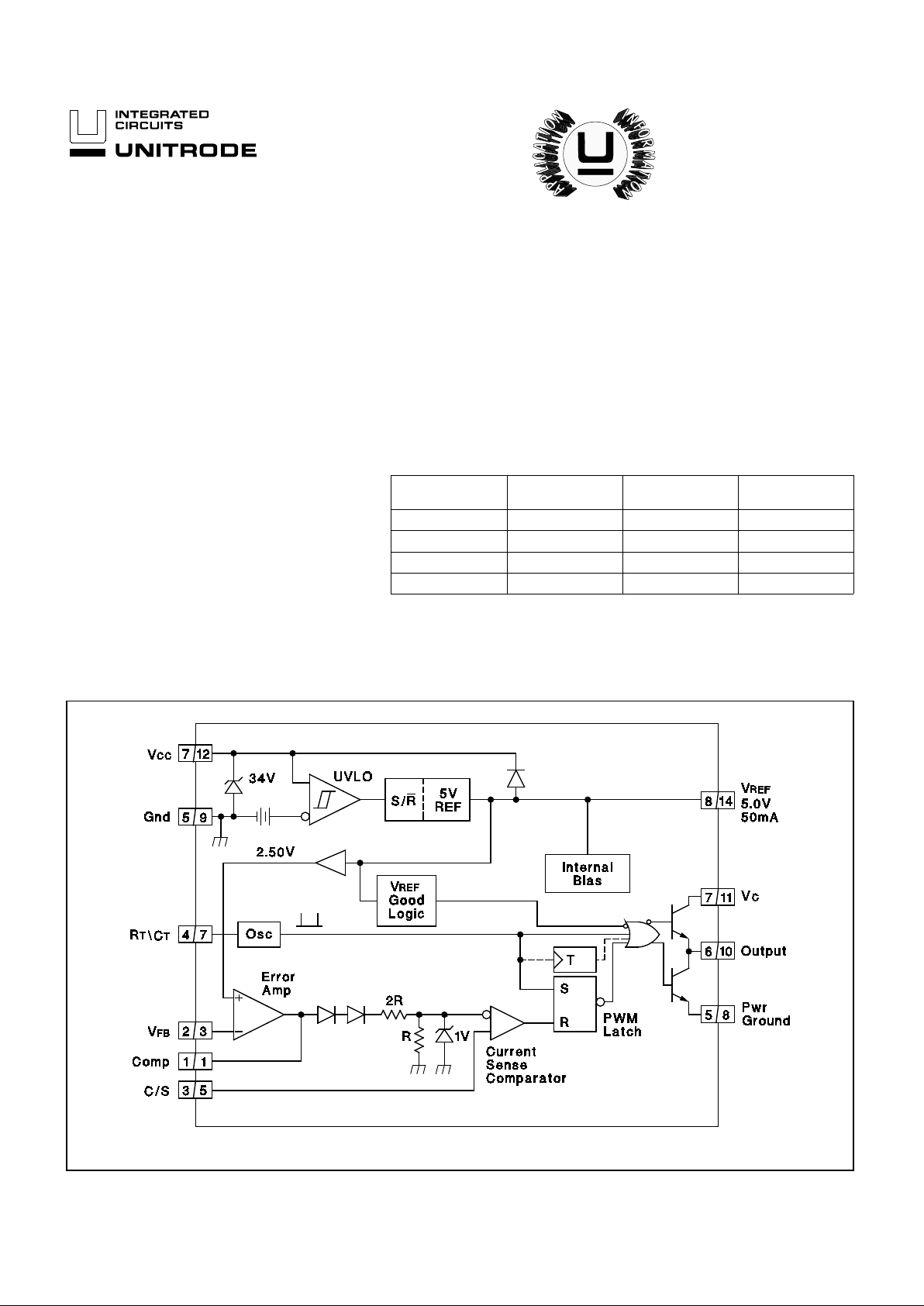
The UC1842A/3A/4A/5A family of control ICs is a pin for pin compatible improved versi on of th e UC3842 /3/4/5 family. Providing the necessary features to control current mode switched mode power
supplies, this family has the following improved features. Start up current is guaranteed to be less than 0.5mA. Oscillator discharge is
trimmed to 8.3mA. During under voltage lockout, the output stage can
sink at least 10mA at less than 1.2V for V CC over 5 V.
The difference between members of this family are shown in the table
below.
UC1842A/3A/4A/5A
UC2842A/3A/4A/5A
UC3842A/3A/4A/5A
BLOCK DIAGRAM
FEATURES DESCRIPTION
Part # UVLO On UVLO Off
Maximum Duty
Cycle
UC1842A 16.0V 10.0V <100%
UC1843A 8.5V 7.9V <100%
UC1844A 16.0V 10.0V <50%
UC1845A 8.5V 7.9V <50%
Note 1: A = DIL-8 Pin Number. B = SO-14 Pin Num be r .
Note 2: Toggle f lip flop use d only in 1844A and 1845A.
A/B
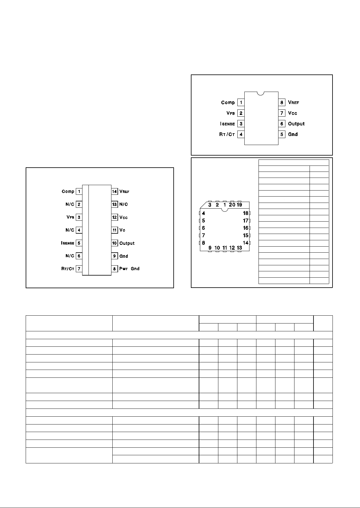
PACKAGE PIN FUNCTION
FUNCTION PIN
N/C
1
Comp 2
N/C 3-4
VFB 5
N/C 6
ISENSE 7
N/C 8-9
RT/CT 10
N/C 11
Pwr Gnd 12
Gnd 13
N/C 14
Output 15
N/C 16
VC 17
VCC 18
N/C 19
VREF 20
DIL-8, SOIC-8 (TOP VIEW)
J or N, D8 Package
CONNECTION DIAG RAMS
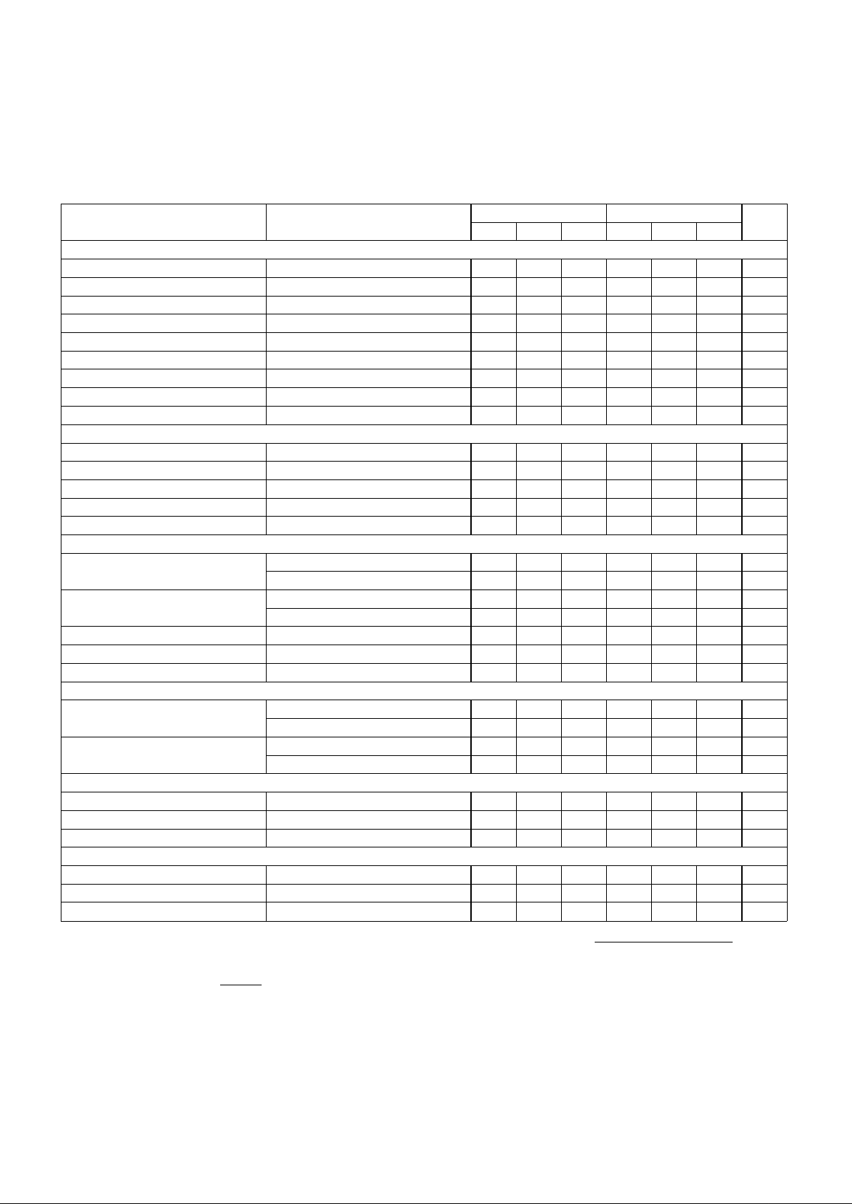
ELECTRICAL CHARACTERISTICS
Unless otherwise stated, these specifications apply for -55°C ≤ TA ≤ 125°C for t h e
UC184xA; -40°C ≤ T
A ≤ 85°C for the UC284xA; 0 ≤ TA ≤ 70°C for the UC384xA; VCC = 15V (Note 5); RT = 10k; CT = 3.3nF; TA = TJ; Pin
numbers refer to DIL-8.
PARAMETER TEST CONDITIONS
UC184xA\UC284xA UC384xA
UNITS
MIN. TYP. MAX. MIN. TYP. MAX.
Reference Sect ion
Output Voltage T
J
= 25°C, IO = 1mA 4.95 5.00 5.05 4.90 5.00 5.10 V
Line Regulation 12 ≤≤ V
IN ≤≤ 25V 6 20 6 20 mV
Load Regulat io n 1 ≤≤ I
O ≤≤ 20mA 6 25 6 25 mV
Temp. Stabilit y (Note 2, Note 7) 0.2 0.4 0.2 0.4 mV/°C
Total Output Variation Line, Load, Temp. 4.9 5.1 4.82 5.18 V
Output Noise Voltage 10Hz ≤≤ f ≤≤ 10kHz
T
J = 25°C (Note 2) 50 50 µV
Long Term Sta bi lity T
A = 125°C, 1000Hrs. (Note 2) 525 525mV
Output Short Circuit -30 -100 -180 -30 -100 -180 mA
Oscillator Section
Initial Accuracy T
J = 25°C (Note 6) 47 52 57 47 52 57 kHz
Voltage Sta b ility 12 ≤≤ V
CC ≤≤ 25V 0.2 1 0.2 1 %
Temp. Stability T
MIN ≤≤ TA ≤≤ TMAX
(Note 2) 5 5 %
Amplitude V
PIN 4 peak to peak (Note 2) 1.7 1.7 V
Discharge Current T
J = 25°C, VPIN 4 = 2V (Note 8) 7.8 8.3 8.8 7.8 8.3 8.8 mA
V
PIN 4 = 2V (Note 8) 7.5 8.8 7.6 8.8 mA
ABSOLUTE MAXIMUM RATINGS (Not e 1)
Note 1. All voltages are with respe ct to Grou nd, Pin 5. Curren ts
are positive into, negative o u t of the spe cified termin al. Co n sult
Packaging Section of Datab ook for therm al limita tion s and co nsiderations of pac kage s. Pin numb ers refer to DIL packa ge only.
PLCC-20, LCC-20
(TOP VIEW)
Q, L Packages
UC1842A/3A/4A/5A
UC2842A/3A/4A/5A
UC3842A/3A/4A/5A
Supply Voltage (Low Imped ance Source) . . . . . . . . . . . . . . 30V
Supply Voltage (I
CC mA). . . . . . . . . . . . . . . . . . . . . Self Limiting
Output Current . . . . . . . . . . . . . . . . . . . . . . . . . . . . . . . . . . . ±1A
Output Energy ( Capac itive Lo ad). . . . . . . . . . . . . . . . . . . . . 5µJ
Analog Inputs (Pins 2, 3) . . . . . . . . . . . . . . . . . . -0.3V to +6.3V
Error Amp Output Sink Curre nt . . . . . . . . . . . . . . . . . . . . 10mA
Power Dissipation at T
A ≤ 25°C (DIL-8). . . . . . . . . . . . . . . . 1W
Storage Tempe rature Rang e . . . . . . . . . . . . . -65°C to +150°C
Lead Temperat ure (Solde ring, 10 Sec onds ) . . . . . . . . . . 300°C
SOIC-14 (TOP VIEW)
D Package
2
PARAMETER TEST CONDITIONS
UC184xA\UC284xA UC384xA
UNITS
MIN. TYP. MAX. MIN. TYP. MAX.
Error Amp Sectio n
Input Voltage V
PIN 1 = 2.5V 2.45 2.50 2.55 2.42 2.50 2.58 V
Input Bias Current -0.3 -1 -0.3 -2 µA
A
VOL 2 ≤ VO ≤ 4V 65 90 65 90 dB
Unity Gain Bandwidth T
J = 25°C (Note 2) 0.7 1 0.7 1 MHz
PSRR 12 ≤ V
CC ≤ 25V 6070 6070 dB
Output Sink Current V
PIN 2 = 2.7V, VPIN 1 = 1.1V 2 6 2 6 mA
Output Source Current V
PIN 2 = 2.3V, VPIN 1 = 5V -0.5 -0.8 -0.5 -0.8 mA
V
OUT High VPIN 2 = 2.3V, RL = 15k to ground 5 6 5 6 V
V
OUT Low VPIN 2 = 2.7V, RL = 15k to Pin 8 0.7 1.1 0.7 1.1 V
Current Sense Section
Gain (Note 3, Note 4) 2.85 3 3.15 2.85 3 3.15 V/V
Maximum Input Signal V
PIN 1 = 5V (Note 3) 0.9 1 1.1 0.9 1 1.1 V
PSRR 12 ≤ V
CC ≤ 25V (Note 3) 70 70 dB
Input Bias Current -2 -10 -2 -10 µA
Dela y to Output V
PIN 3 = 0 to 2V (Note 2) 150 300 150 300 ns
Output Secti on
Output Low Level I
SINK = 20mA 0.1 0.4 0.1 0.4 V
I
SINK = 200mA 15 2.2 15 2.2 V
Output High Level I
SOURCE = 20mA 13 13.5 13 13.5 V
I
SOURCE = 200m A 12 13.5 12 13.5 V
Rise Time T
J = 25°C, CL = 1nF (Note 2) 50 150 50 150 ns
Fall Time T
J = 25°C, CL = 1nF (Note 2) 50 150 50 150 ns
UVLO Saturation V
CC = 5V, ISINK = 10mA 0.7 1.2 0.7 1.2 V
Under-Vol t age Lo ckou t Secti on
Start Threshold x842A/4A 15 16 17 14.5 16 17.5 V
x843A/5A 7.8 8.4 9.0 7.8 8.4 9.0 V
Min. Operat io n Voltage Af te r x842A/4A 9 10 11 8.5 10 11.5 V
Turn On x843A/5A 7.0 7.6 8.2 7.0 7.6 8.2 V
PWM Sectio n
Maximum Duty Cycle x842A/3A 94 96 100 94 96 100 %
x844A/5A 47 48 50 47 48 50 %
Minimum Duty Cycle 0 0 %
Total Standb y Current
Start-Up Cur rent 0.3 0.5 0.3 0.5 mA
Operating Supply Current V
PIN 2 = VPIN 3 = 0V 11 17 11 17 mA
V
CC Zener Voltage ICC = 25mA 30 34 30 34 V
UC1842A/3A/4A/5A
UC2842A/3A/4A/5A
UC3842A/3A/4A/5A
Note 2: These param et ers, alt hou gh gua ran teed, are not 100%
tested in production.
Note 3: Paramete r measu red at trip poin t of latch with V
PIN2
= 0.
Note 4: Gain defined as : A
=
∆
V
PIN 1
∆
V
PIN 3
; 0 ≤ V
PIN 3
≤ 0.8V.
Note 5: Adjust V
CC
above the start thresho ld before setting at
15V .
Note 6: Out put frequency equals oscillator frequency for the
UC1842A and UC1843A. Output frequency is one ha lf
oscillator freque ncy f or the UC1844A and UC1845A.
Note 7: "Temperatu re sta b i lit y, som etimes re fe rr ed to as a ve r ag e
temperature coeffic ient , is describe d by t he equ atio n:
Temp
Stability
=
V
REF
(
max
) −
V
REF
(
min
)
T
J
(
max
) −
T
J
(
min
)
.
V
REF
(max) and V
REF
(min) are the maximum & mini mum reference voltag e me asur ed ov er the ap propriate
temperature range. Note that the extr em es in volt age
do not necessarily occur at the extremes in tempera ture."
Note 8: This paramet er is measure d w ith R
T
= 10kΩ to V
REF
.
This contribut es approximat ely 300
µ
A of current to t h e
measurement. The total current flowing into t he R
T/CT
pin will be approximately 300µA higher than the meas-
ured value.
ELECTRICAL CHARACTERISTICS (cont.) Unless otherwise stated, these specifications apply for -55°C ≤ TA ≤ 125°C for
the UC184xA; -40°C ≤ T
A ≤ 85°C for the UC284xA; 0 ≤ TA ≤ 70°C for the UC384xA; VCC = 15V (Note 5); RT = 10k; CT = 3.3nF; TA = TJ;
Pin numbers re fe r to DIL-8.
3

Error Amp Confi g urati on
UC1842A/3A/4A/5A
UC2842A/3A/4A/5A
UC3842A/3A/4A/5A
Under-Voltage L ocko u t
During UVLO, the Out put is low.
Current Sense Circuit
A sma ll RC filter may be required to suppr ess swit ch t ransient s.
Peak Current (I
S) is Determined By The Formula
I
SMAX ≈
1.0V
R
S
Error Amp can Source and Sink up to 0.5m A, and S ink up to 2mA.
4

APPLICATIONS DATA (cont. )
Open-Loop Labo rato ry Test Fixt ure
UC1842A/3A/4A/5A
UC2842A/3A/4A/5A
UC3842A/3A/4A/5A
Output Satura ti on Cha rac ter i stics Err or Amp lifie r Ope n-L oop Fre quen cy Re spon se
Oscillator Section
Oscillator Frequ ency vs Timi ng Resis tan ce
Maximum Duty Cycle vs Timing Resistor
High peak currents associa te d with capacit ive loads necessitate careful grou nding tech niques . Timing and bypas s capacitors should be connected close to pin 5 in a single point
ground. The transis to r and 5k potent iom et er are used to s am ple the oscillator wavef orm and apply an adjust able ram p to
pin 3.
5

Off-line Flyb ack Regu lato r
Slope Compen sati on
APPLICATIONS DATA (cont. )
UC1842A/3A/4A/5A
UC2842A/3A/4A/5A
UC3842A/3A/4A/5A
Power Supply Specifications
1. Input Voltage 95VAC t o 130V A
(50 Hz/60Hz)
2. Line Isolatio n 3750V
3. Switching Frequency 40kHz
4. Efficiency @ Full Loa d 70%
5. Output Voltage:
A. +5V, ±5%; 1A to 4A load
Ripple voltage: 50mV P-P Max
B. +12V, ±3%; 0.1A to 0.3A load
Ripple voltage: 100mV P-P Max
C. -12V ,±3%; 0.1A to 0.3A load
Ripple voltage: 100mV P-P Max
A frac tion of the os cillator ramp ca n be resist iv ely
summed with the cur ren t sense sign al to pr ovide slope
compensat ion for conve rter s requiring d u ty cycles ov er
50%.
Note that capacito r, C, forms a filter wit h R2 to suppr ess
the leading edge switch spikes.
UNITRODE INTEGRATED CIRCUITS
7 CONTINENTAL BLVD. • MERRIMACK, NH 03054
TEL. (603) 424-2410 • FAX (603)424-3460
6

IMPORTANT NOTICE
T exas Instruments and its subsidiaries (TI) reserve the right to make changes to their products or to discontinue
any product or service without notice, and advise customers to obtain the latest version of relevant information
to verify, before placing orders, that information being relied on is current and complete. All products are sold
subject to the terms and conditions of sale supplied at the time of order acknowledgement, including those
pertaining to warranty, patent infringement, and limitation of liability.
TI warrants performance of its semiconductor products to the specifications applicable at the time of sale in
accordance with TI’s standard warranty. Testing and other quality control techniques are utilized to the extent
TI deems necessary to support this warranty. Specific testing of all parameters of each device is not necessarily
performed, except those mandated by government requirements.
CERT AIN APPLICATIONS USING SEMICONDUCTOR PRODUCTS MAY INVOLVE POTENTIAL RISKS OF
DEATH, PERSONAL INJURY, OR SEVERE PROPERTY OR ENVIRONMENTAL DAMAGE (“CRITICAL
APPLICATIONS”). TI SEMICONDUCTOR PRODUCTS ARE NOT DESIGNED, AUTHORIZED, OR
WARRANTED TO BE SUITABLE FOR USE IN LIFE-SUPPORT DEVICES OR SYSTEMS OR OTHER
CRITICAL APPLICATIONS. INCLUSION OF TI PRODUCTS IN SUCH APPLICA TIONS IS UNDERSTOOD T O
BE FULLY AT THE CUSTOMER’S RISK.
In order to minimize risks associated with the customer’s applications, adequate design and operating
safeguards must be provided by the customer to minimize inherent or procedural hazards.
TI assumes no liability for applications assistance or customer product design. TI does not warrant or represent
that any license, either express or implied, is granted under any patent right, copyright, mask work right, or other
intellectual property right of TI covering or relating to any combination, machine, or process in which such
semiconductor products or services might be or are used. TI’s publication of information regarding any third
party’s products or services does not constitute TI’s approval, warranty or endorsement thereof.
Copyright 1999, Texas Instruments Incorporated
 Loading...