

UC2842AQ, UC2843AQ, UC2844AQ, UC2845AQ
CURRENT-MODE PWM CONTROLLER
SGLS164 – APRIL 2003
D Extended Temperature Performance of
–40°C to 125°C
D Optimized for Off-line and DC to DC
Converters
D Low Start Up Current (<0.5 mA)
D Trimmed Oscillator Discharge Current
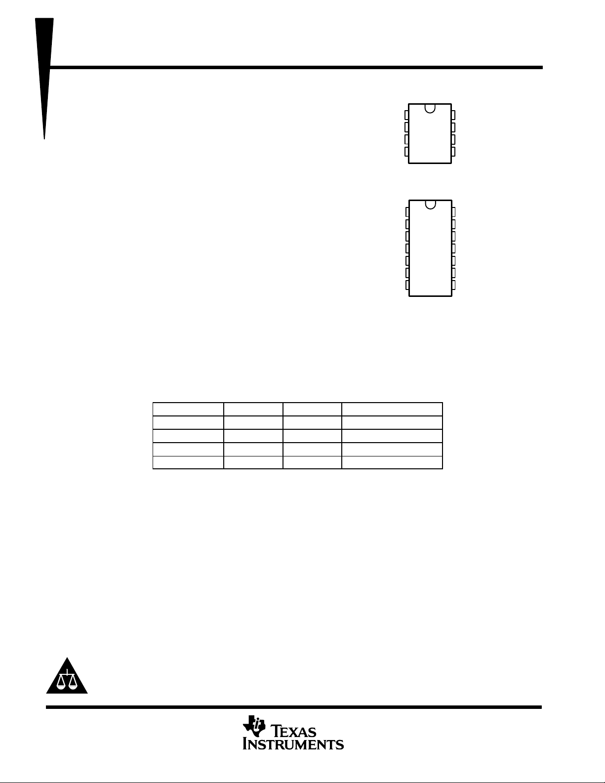
D 8-PIN PACKAGE
COMP
V
FB
I
SENSE
RT/C
T
(TOP VIEW)
1
2
3
4
8
7
6
5
V
REF
V
CC
OUTPUT
GND
D Automatic Feed Forward Compensation
D Pulse-by-Pulse Current Limiting
D Enhanced Load Response Characteristics
D Under-Voltage Lockout With Hysteresis
D Double Pulse Suppression
D High Current Totem Pole Output
D Internally Trimmed Bandgap Reference
D 500 kHz Operation
D Low R
description
The UC2842A/3A/4A/5A family of control ICs is a pin for pin compatible improved version of the UC2842/3/4/5
family . Providing the necessary features to control current mode switched mode power supplies, this family has the
following improved features. Start up current is guaranteed to be less than 0.5 mA. Oscillator discharge is trimmed
to 8.3 mA. During under voltage lockout, the output stage can sink at least 10 mA at less than 1.2 V for V
5 V.
Error Amp
O
D 14-PIN PACKAGE
(TOP VIEW)
COMP
I
SENSE
R
NC
V
FB
NC
NC
T/CT
1
2
3
4
5
6
7
14
13
12
11
10
9
8
V
REF
NC
V
CC
V
C
OUTPUT
GND
PWR GND
CC
over
The difference between members of this family are shown in the table below.
PART NUMBER UVLO ON UVLO OFF MAXIMUM DUTY CYCLE
UC2842A 16 V 10 V <100%
UC2843A 8.5 V 7.9 V <100%
UC2844A 16 V 10 V <50%
UC2845A 8.5 V 7.9 V <50%
Please be aware that an important notice concerning availability, standard warranty, and use in critical applications of
Texas Instruments semiconductor products and disclaimers thereto appears at the end of this data sheet.
PRODUCTION DATA information is current as of publication date.
Products conform to specifications per the terms of Texas Instruments
standard warranty. Production processing does not necessarily include
testing of all parameters.
POST OFFICE BOX 655303 • DALLAS, TEXAS 75265
Copyright 2003, Texas Instruments Incorporated
1
UC2842AQ, UC2843AQ, UC2844AQ, UC2845AQ
CURRENT-MODE PWM CONTROLLER
SGLS164 – APRIL 2003
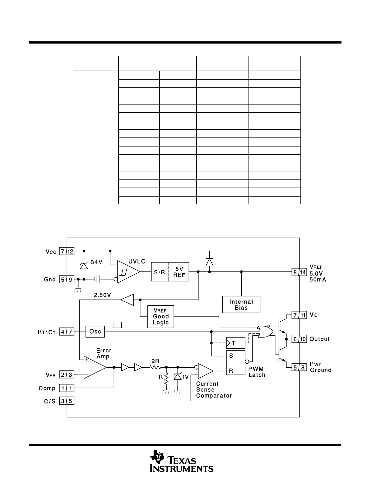
block diagram
ORDERING INFORMATION
T
A
SOIC-8 – D8 Tape and reel UC2842AQD8R 2842AQ
SOIC-8 – D8 Tube UC2842AQD8 2842AQ
SOIC-14 – D Tape and reel UC2842AQDR 2842AQ
SOIC-14 – D Tube UC2842AQD 2842AQ
SOIC-8 – D8 Tape and reel UC2843AQD8R 2843AQ
SOIC-8 – D8 Tube UC2843AQD8 2843AQ
SOIC-14 – D Tape and reel UC2843AQDR 2843AQ
°
–40°C to 125°C
†
Package drawings, standard packing quantities, thermal data, symbolization, and PCB design guidelines
are available at www.ti.com/sc/package.
SOIC-14 – D Tube UC2843AQD 2843AQ
°
SOIC-8 – D8 Tape and reel UC2844AQD8R 2844AQ
SOIC-8 – D8 Tube UC2844AQD8 2844AQ
SOIC-14 – D Tape and reel UC2844AQDR 2844AQ
SOIC-14 – D Tube UC2844AQD 2844AQ
SOIC-8 – D8 Tape and reel UC2845AQD8R 2845AQ
SOIC-8 – D8 Tube UC2845AQD8 2845AQ
SOIC-14 – D Tape and reel UC2845AQDR 2845AQ
SOIC-14 – D Tube UC2845AQD 2845AQ
PACKAGE
‡
ORDERABLE
PART NUMBER
†
TOP-SIDE
MARKING
NOTES: 1. A = DIL-8 Pin Number. B = SO-14 Pin Number.
2
2. Toggle flip flop used only in 2844A and 2845A.
POST OFFICE BOX 655303 • DALLAS, TEXAS 75265
Ordering Information
284
UC
UC2842AQ, UC2843AQ, UC2844AQ, UC2845AQ
CURRENT-MODE PWM CONTROLLER
SGLS164 – APRIL 2003
4
Q
D
A
R
TAPE and REEL INDICATOR
PACKAGE
D = Plastic SOIC, 14 pin
D8 = Plastic SOIC, 8 pin
AUTOMOTIVE TEMPERATURE RANGE INDICATOR
IMPROVED PERFORMANCE INDICATOR
PRODUCT OPTION
2 through 5
POST OFFICE BOX 655303 • DALLAS, TEXAS 75265
3
UC2842AQ, UC2843AQ, UC2844AQ, UC2845AQ
CURRENT-MODE PWM CONTROLLER
SGLS164 – APRIL 2003
absolute maximum ratings over operating free-air temperature range (unless otherwise noted)
voltage (low impedance source) 30 V. . . . . . . . . . . . . . . . . . . . . . . . . . . . . . . . . . . . . . . . . . . . . . . . . . . . . . . . .
V
CC
V
voltage (ICC mA) self limiting. . . . . . . . . . . . . . . . . . . . . . . . . . . . . . . . . . . . . . . . . . . . . . . . . . . . . . . . . . . . . . . .
CC
Output current, I
±1 A. . . . . . . . . . . . . . . . . . . . . . . . . . . . . . . . . . . . . . . . . . . . . . . . . . . . . . . . . . . . . . . . . . . . . . . . .
O
†‡
Output energy (capacitive load) 5 µJ. . . . . . . . . . . . . . . . . . . . . . . . . . . . . . . . . . . . . . . . . . . . . . . . . . . . . . . . . . . . . .
Analog Inputs (pins 3, 5) –0.3 V to 6.3 V. . . . . . . . . . . . . . . . . . . . . . . . . . . . . . . . . . . . . . . . . . . . . . . . . . . . . . . . . . .
Error Amp Output Sink current 10 mA. . . . . . . . . . . . . . . . . . . . . . . . . . . . . . . . . . . . . . . . . . . . . . . . . . . . . . . . . . . . .
Power Dissipation at T
Package thermal impedance, θ
Storage temperature range, T
< +25_C (D package) 1 W. . . . . . . . . . . . . . . . . . . . . . . . . . . . . . . . . . . . . . . . . . . . . . . . . .
A
(see Note 1): D (8-pin) package 97°C/W. . . . . . . . . . . . . . . . . . . . . . . . . . . .
JA
stg
–65_C to 150_C. . . . . . . . . . . . . . . . . . . . . . . . . . . . . . . . . . . . . . . . . . . . . . . . . . . .
Lead temperature soldering 1,6 mm (1/16 inch) from case for 10 seconds 260_C. . . . . . . . . . . . . . . . . . . . . . .
†
Stresses beyond those listed under “absolute maximum ratings” may cause permanent damage to the device. These are stress ratings only, and
functional operation of the device at these or any other conditions beyond those indicated under “recommended operating conditions” is not implied.
Exposure to absolute-maximum-rated conditions for extended periods may affect device reliability.
‡
Unless otherwise indicated, voltages are reference to ground and currents are positive into and negative out of the specified terminals.
NOTE 1: Long term high–temperature storage and/or extended use at maximum recommended operating conditions may result in a reduction of
overall device life. See http://www.ti.com/ep_quality for additional information on enhanced plastic packaging.
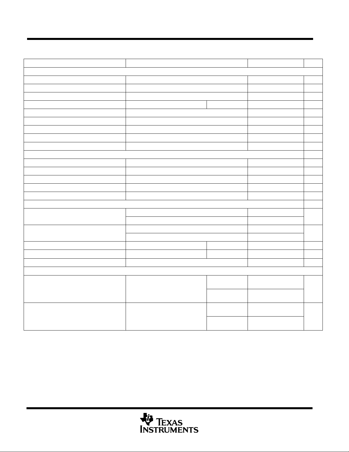
electrical characteristics, TA = –40_C to 125_C, VCC = 15 V (see Note 1), RT = 10 kΩ, CT = 3.3 nF, and
T
= TJ (unless otherwise stated)
A
PARAMETER TEST CONDITIONS MIN TYP MAX UNITS
Reference Section
Output voltage
Line regulation voltage VIN = 12 V to 25 V 6 20 mV
Load regulation voltage IO = 1 mA to 20 mA 6 25 mV
T emperature stability See Notes 2 and 3 0.2 0.4
Total output variation voltage Line, Load, Temp. 4.9 5.1 V
Output noise voltage
Long term stability 1000 hours, See Note 2
Output short-circuit current –30 –100 –180 mA
Oscillator Section
Initial accuracy See Note 4
Voltage stability VCC = 12 V to 25 V 0.2 1 %
T emperature stability TA = MIN to MAX, See Note 2 5 %
Amplitude peak-to-peak V pin 7, See Note 2 1.7 V
Discharge current V pin 7 = 2 V, See Note 5
TJ = 25_C, IO = 1 mA
f = 10 Hz to 10 kHz,
See Note 2
TJ = 25_C
TA = 125_C
TJ = 25_C
TJ = 25_C
TJ = Full range 7.5 8.8
4.95 5.0 5.05 V
mV/_C
50
5 25 mV
47 52 57 kHz
7.8 8.3 8.8
µV
mA
4
POST OFFICE BOX 655303 • DALLAS, TEXAS 75265
UC2842AQ, UC2843AQ, UC2844AQ, UC2845AQ
CURRENT-MODE PWM CONTROLLER
SGLS164 – APRIL 2003
electrical characteristics, TA = –40_C to 125_C, VCC = 15 V (see Note 1), RT = 10 kΩ, CT = 3.3 nF, and
T
= TJ (unless otherwise stated)
A
PARAMETER TEST CONDITIONS MIN TYP MAX UNITS
Error Amplifier Section
Input voltage COMP = 2.5 V 2.45 2.5 2.55 V
Input bias current –0.3 –1
Open loop voltage gain (A
Unity gain bandwidth See Note 2
PSRR VCC = 12 V to 25 V 60 70 dB
Output sink current FB = 2.7 V, COMP = 1.1 V 2 6 mA
Output source current FB = 2.3 V, COMP = 5 V –0.5 –0.8 mA
V
high
OUT
V
low
OUT
Current Sense Section
Gain See Notes 6 and 7 2.85 3 3.15 V/V
Maximum input signal COMP = 5 V, See Note 6 0.9 1 1.1 V
PSRR VCC = 12 V to 25 V,See Note 6 70 dB
Input bias current –2 –10
Delay to output I
Output Section (OUT)
Low-level output voltage
High-level output voltage
Rise time CL = 1 nF, See Note 2
Fall time CL = 1 nF, See Note 2
UVLO saturation VCC = 5 V, I
Undervoltage Lockout Section
Start threshold
Minimum operation voltage after turn on
VOL)
VO = 2 V to 4 V 65 90 dB
TJ = 25_C
FB = 2.3 V, RL = 15 kΩ to GND
FB = 2.7 V, RL = 15 kΩ to V
= 0 V to 2 V, See Note 2 150 300 ns
SENSE
I
= 20 mA 0.1 0.4
OUT
I
= 200 mA 15 2.2
OUT
I
= –20 mA 13 13.5
OUT
I
= –200 mA 12 13.5
OUT
= 10 mA 0.7 1.2 V
OUT
REF
TJ = 25_C
TJ = 25_C
UC2842A,
UC2844A
UC2843A,
UC2845A
UC2842A,
UC2844A
UC2843A,
UC2845A
0.7 1 MHz
5 6 V
0.7 1.1 V
50 150 ns
50 150 ns
15 16 17
7.8 8.4 9
9 10 11
7 7.6 8.2
µA
µA
V
V
V
V
POST OFFICE BOX 655303 • DALLAS, TEXAS 75265
5

UC2842AQ, UC2843AQ, UC2844AQ, UC2845AQ
CURRENT-MODE PWM CONTROLLER
SGLS164 – APRIL 2003
electrical characteristics, TA = –40_C to 125_C, VCC = 15 V (see Note 1), RT = 10 kΩ, CT = 3.3 nF, and
T
= TJ (unless otherwise stated)
A
PARAMETER TEST CONDITIONS MIN TYP MAX UNITS
PWM Section
Maximum duty cycle
Minimum duty cycle 0 %
Total Standby Current
Start-up current 0.3 0.5 mA
Operating supply current FB = 0 V, SENSE = 0 V 11 17 mA
VCC internal zener voltage ICC = 25 mA 30 34 V
NOTES: 1. Adjust VCC above the start threshold before setting at 15 V .
2. Not production tested.
3. Temperature stability, sometimes referred to as average temperature coefficient, is described by the equation:
V
(max) – V
Temp Stability =
over the appropriate temperature range. Note that the extremes in voltage do not necessarily occur at the extremes in temperature.
4. Output frequency equals oscillator frequency for the UC2842A and UC2843A. Output frequency is one half oscillator frequency for the
UC2844A and UC2845A.
5. This parameter is measured with RT = 10 kΩ to V
current flowing into the R
6. Parameter measured at trip point of latch with VFB at 0 V.
7. Gain is defined by:
REF
TJ (max) – TJ (min)
T/C
DV
A =
DV
REF
pin will be approximately 300 µA higher than the measured value.
; 0 v V
COMP
SENSE
(min)
SENSE
. V
(max) and V
REF
. This contributes approximately 300 µA of current to the measurement. The total
REF
v 0.8 V.
REF
UC2842A, UC2843A 94 96 100
UC2844A, UC2845A 47 48 50
(min) are the maximum and minimum reference voltage measured
%
RAMETER MEASUREMENT INFORMATION
Error Amp can source and sink up to 0.5 mA, and sink up to 2 mA.
Figure 1. Error Amp Configuration
PA
6
POST OFFICE BOX 655303 • DALLAS, TEXAS 75265

UC2842AQ, UC2843AQ, UC2844AQ, UC2845AQ
CURRENT-MODE PWM CONTROLLER
PARAMETER MEASUREMENT INFORMATION
During UVLO, the Output is low.
Figure 2. Under Voltage Lockout
SGLS164 – APRIL 2003
Peak Current (Is) is Determined By The Formula:
1.0V
IsmaxȀ
A small RC filter may be required to supress switch transients.
RS
Figure 3. Current Sense Circuit
POST OFFICE BOX 655303 • DALLAS, TEXAS 75265
7

UC2842AQ, UC2843AQ, UC2844AQ, UC2845AQ
CURRENT-MODE PWM CONTROLLER
SGLS164 – APRIL 2003
PARAMETER MEASUREMENT INFORMATION
Output Saturation Characteristics
Figure 4
Oscillator Frequency vs Timing Resistance
Error Amplifier Open-Loop Frequency Response
Figure 5
AP
PLICATION INFORMATION
Maximum Duty Cycle vs Timing Resistor
Figure 6. Oscillator
8
POST OFFICE BOX 655303 • DALLAS, TEXAS 75265

UC2842AQ, UC2843AQ, UC2844AQ, UC2845AQ
CURRENT-MODE PWM CONTROLLER
SGLS164 – APRIL 2003
APPLICATION INFORMATION
High peak currents associated with capacitive loads necessitate careful grounding techniques. Timing and bypass capacitors should be
connected close to pin 5 in a single point ground. The transistor and 5k potentiometer are used to sample the oscillator waveform and apply an
adjustable ramp to pin 3.
Figure 7. Open-Loop Laboratory Text Fixture
A fraction of the oscillator ramp can be resistively summed
with the current sense signal to provide slope compensation
for converters requiring duty cycles over 50%.
Note that capacitor, C, forms a filter with R2 to suppress the
leading edge switch spikes.
Figure 8. Slope Complression
POST OFFICE BOX 655303 • DALLAS, TEXAS 75265
9

UC2842AQ, UC2843AQ, UC2844AQ, UC2845AQ
CURRENT-MODE PWM CONTROLLER
SGLS164 – APRIL 2003
APPLICATION INFORMATION
Power Supply Specifications
1. Input Voltage 95VAC to 130VAC (50Hz/60Hz)
2. Line Isolation 3750V
3. Switching Frequency 40 kHz
4. Efficiency, Full Load 70%
5. Output Voltage:
A. +5V, ±5%; 1A to 4A Load
B. +12V, ±3%; 0.1A to 0.3A Load Ripple voltage: 100 mV P-P Max
C. –12V, ±3%; 0.1A to 0.3A Load Ripple voltage: 100 mV P-P Max
Figure 9. Off-Line Flyback Regulator
10
POST OFFICE BOX 655303 • DALLAS, TEXAS 75265

PACKAGE OPTION ADDENDUM
www.ti.com
8-Sep-2007
PACKAGING INFORMATION
Orderable Device Status
(1)
Package
Type
Package
Drawing
Pins Package
Qty
Eco Plan
UC2842AQD ACTIVE SOIC D 14 50 Green (RoHS &
no Sb/Br)
UC2842AQD8 ACTIVE SOIC D 8 75 Green (RoHS &
no Sb/Br)
UC2842AQD8R ACTIVE SOIC D 8 2500 Green (RoHS &
no Sb/Br)
UC2842AQDR ACTIVE SOIC D 14 2500 Green (RoHS &
no Sb/Br)
UC2843AQD ACTIVE SOIC D 14 50 Green (RoHS &
no Sb/Br)
UC2843AQD8 ACTIVE SOIC D 8 75 Green (RoHS &
no Sb/Br)
UC2843AQD8R ACTIVE SOIC D 8 2500 Green (RoHS &
no Sb/Br)
UC2843AQDR ACTIVE SOIC D 14 2500 Green (RoHS &
no Sb/Br)
UC2845AQD ACTIVE SOIC D 14 50 Green (RoHS &
no Sb/Br)
UC2845AQD8 ACTIVE SOIC D 8 75 Green (RoHS &
no Sb/Br)
UC2845AQD8R ACTIVE SOIC D 8 2500 Green (RoHS &
no Sb/Br)
UC2845AQDR ACTIVE SOIC D 14 2500 Green (RoHS &
no Sb/Br)
(1)
The marketing status values are defined as follows:
ACTIVE: Product device recommended for new designs.
LIFEBUY: TI has announced that the device will be discontinued, and a lifetime-buy period is in effect.
NRND: Not recommended for new designs. Device is in production to support existing customers, but TI does not recommend using this part in
a new design.
PREVIEW: Device has been announced but is not in production. Samples may or may not be available.
OBSOLETE: TI has discontinued the production of the device.
(2)
Lead/Ball Finish MSL Peak Temp
CU NIPDAU Level-1-260C-UNLIM
CU NIPDAU Level-1-260C-UNLIM
CU NIPDAU Level-1-260C-UNLIM
CU NIPDAU Level-1-260C-UNLIM
CU NIPDAU Level-1-260C-UNLIM
CU NIPDAU Level-1-260C-UNLIM
CU NIPDAU Level-1-260C-UNLIM
CU NIPDAU Level-1-260C-UNLIM
CU NIPDAU Level-1-260C-UNLIM
CU NIPDAU Level-1-260C-UNLIM
CU NIPDAU Level-1-260C-UNLIM
CU NIPDAU Level-1-260C-UNLIM
(3)
(2)
Eco Plan - The planned eco-friendly classification: Pb-Free (RoHS), Pb-Free (RoHS Exempt), or Green (RoHS & no Sb/Br) - please check
http://www.ti.com/productcontent for the latest availability information and additional product content details.
TBD: The Pb-Free/Green conversion plan has not been defined.
Pb-Free (RoHS): TI's terms "Lead-Free" or "Pb-Free" mean semiconductor products that are compatible with the current RoHS requirements
for all 6 substances, including the requirement that lead not exceed 0.1% by weight in homogeneous materials. Where designed to be soldered
at high temperatures, TI Pb-Free products are suitable for use in specified lead-free processes.
Pb-Free (RoHS Exempt): This component has a RoHS exemption for either 1) lead-based flip-chip solder bumps used between the die and
package, or 2) lead-based die adhesive used between the die and leadframe. The component is otherwise considered Pb-Free (RoHS
compatible) as defined above.
Green (RoHS & no Sb/Br): TI defines "Green" to mean Pb-Free (RoHS compatible), and free of Bromine (Br) and Antimony (Sb) based flame
retardants (Br or Sb do not exceed 0.1% by weight in homogeneous material)
(3)
MSL, Peak Temp. -- The Moisture Sensitivity Level rating according to the JEDEC industry standard classifications, and peak solder
temperature.
Important Information and Disclaimer:The information provided on this page represents TI's knowledge and belief as of the date that it is
provided. TI bases its knowledge and belief on information provided by third parties, and makes no representation or warranty as to the
accuracy of such information. Efforts are underway to better integrate information from third parties. TI has taken and continues to take
reasonable steps to provide representative and accurate information but may not have conducted destructive testing or chemical analysis on
incoming materials and chemicals. TI and TI suppliers consider certain information to be proprietary, and thus CAS numbers and other limited
information may not be available for release.
Addendum-Page 1

PACKAGE OPTION ADDENDUM
www.ti.com
In no event shall TI's liability arising out of such information exceed the total purchase price of the TI part(s) at issue in this document sold by TI
to Customer on an annual basis.
8-Sep-2007
Addendum-Page 2


IMPORTANT NOTICE
Texas Instruments Incorporated and its subsidiaries (TI) reserve the right to make corrections, modifications, enhancements,
improvements, and other changes to its products and services at any time and to discontinue any product or service without notice.
Customers should obtain the latest relevant information before placing orders and should verify that such information is current and
complete. All products are sold subject to TI’s terms and conditions of sale supplied at the time of order acknowledgment.
TI warrants performance of its hardware products to the specifications applicable at the time of sale in accordance with TI’s
standard warranty. Testing and other quality control techniques are used to the extent TI deems necessary to support this
warranty. Except where mandated by government requirements, testing of all parameters of each product is not necessarily
performed.
TI assumes no liability for applications assistance or customer product design. Customers are responsible for their products and
applications using TI components. To minimize the risks associated with customer products and applications, customers should
provide adequate design and operating safeguards.
TI does not warrant or represent that any license, either express or implied, is granted under any TI patent right, copyright, mask
work right, or other TI intellectual property right relating to any combination, machine, or process in which TI products or services
are used. Information published by TI regarding third-party products or services does not constitute a license from TI to use such
products or services or a warranty or endorsement thereof. Use of such information may require a license from a third party under
the patents or other intellectual property of the third party, or a license from TI under the patents or other intellectual property of TI.
Reproduction of TI information in TI data books or data sheets is permissible only if reproduction is without alteration and is
accompanied by all associated warranties, conditions, limitations, and notices. Reproduction of this information with alteration is an
unfair and deceptive business practice. TI is not responsible or liable for such altered documentation. Information of third parties
may be subject to additional restrictions.
Resale of TI products or services with statements different from or beyond the parameters stated by TI for that product or service
voids all express and any implied warranties for the associated TI product or service and is an unfair and deceptive business
practice. TI is not responsible or liable for any such statements.
TI products are not authorized for use in safety-critical applications (such as life support) where a failure of the TI product would
reasonably be expected to cause severe personal injury or death, unless officers of the parties have executed an agreement
specifically governing such use. Buyers represent that they have all necessary expertise in the safety and regulatory ramifications
of their applications, and acknowledge and agree that they are solely responsible for all legal, regulatory and safety-related
requirements concerning their products and any use of TI products in such safety-critical applications, notwithstanding any
applications-related information or support that may be provided by TI. Further, Buyers must fully indemnify TI and its
representatives against any damages arising out of the use of TI products in such safety-critical applications.
TI products are neither designed nor intended for use in military/aerospace applications or environments unless the TI products are
specifically designated by TI as military-grade or "enhanced plastic." Only products designated by TI as military-grade meet military
specifications. Buyers acknowledge and agree that any such use of TI products which TI has not designated as military-grade is
solely at the Buyer's risk, and that they are solely responsible for compliance with all legal and regulatory requirements in
connection with such use.
TI products are neither designed nor intended for use in automotive applications or environments unless the specific TI products
are designated by TI as compliant with ISO/TS 16949 requirements. Buyers acknowledge and agree that, if they use any
non-designated products in automotive applications, TI will not be responsible for any failure to meet such requirements.
Following are URLs where you can obtain information on other Texas Instruments products and application solutions:
Products Applications
Amplifiers amplifier.ti.com Audio www.ti.com/audio
Data Converters dataconverter.ti.com Automotive www.ti.com/automotive
DSP dsp.ti.com Broadband www.ti.com/broadband
Interface interface.ti.com Digital Control www.ti.com/digitalcontrol
Logic logic.ti.com Military www.ti.com/military
Power Mgmt power.ti.com Optical Networking www.ti.com/opticalnetwork
Microcontrollers microcontroller.ti.com Security www.ti.com/security
RFID www.ti-rfid.com Telephony www.ti.com/telephony
Low Power www.ti.com/lpw Video & Imaging www.ti.com/video
Wireless
Wireless www.ti.com/wireless
Mailing Address: Texas Instruments, Post Office Box 655303, Dallas, Texas 75265
Copyright © 2007, Texas Instruments Incorporated
 Loading...