

FEATURES
• Complete Control for a High Current,
Low Dropout, Linear Regulator
• Fixed 5V or Adjustable Output Voltage
• Accurate 2.5A Current Limiting with
Foldback
• Internal Current Sense Resistor
• Remote Sense for Improved Load
Regulation
• External Shutdown
• Under-Voltage Lockout and Reverse
Voltage Protection
• Thermal Shutdown Protection
• 8 Pin Mini-Dip Package
(Surface Mount also Available)
DESCRIPTI ON
The UC1835/6 families of linear controllers are optimized for the design of low cost, low dropout, linear regulators. Using an external pass
element, dropout voltages of less than 0.5V are readily obtained.
These devices contain a high gain error amplifier, a 250mA output
driver, and a precision reference. I n addition, current sense with foldback provides for a 2.5A peak output current dropping to less than
0.5A at short circuit.
These devices are available in fixed, 5V, (UC1835), or adjustable,
(UC1836), versions. In the fi xed 5 volt version, the only external parts
required are an external pass element, an output capacitor, and a compensation capaci tor. On the adjustable version the output voltage can
be set anywhere from 2.5V to 35V with two external resistors.
Additional features of these devices include under-voltage lockout for
predictable start-up, thermal shutdown and short circuit current limiting
to protect the dri ver device. On the fixed voltage version, a reverse
voltage comparator mini mizes reverse load current in the event of a
negative input to output differential.
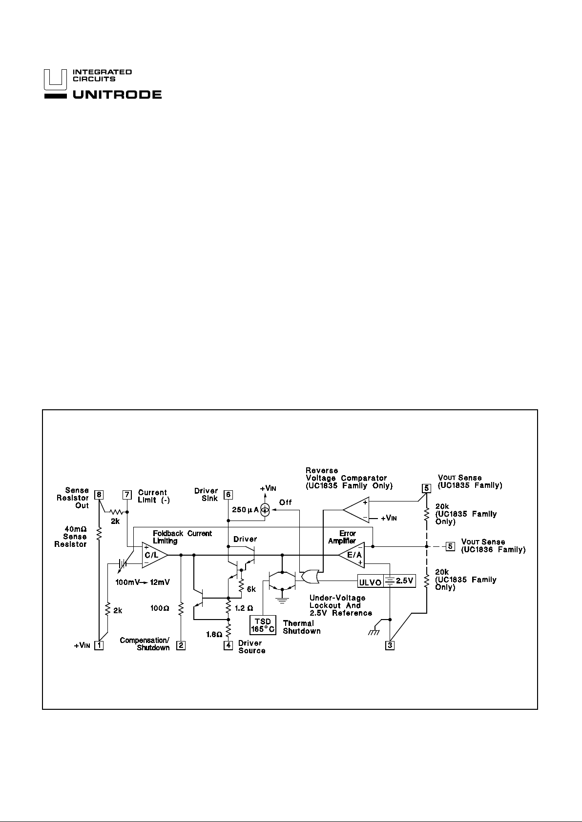
High Efficiency Regulator Controller
BLOCK DIAGRAM
Note: Pin numbers refer to 8-Pin DIL Pack age
UC1835 UC1836
UC2835 UC2836
UC3835 UC3836
8/94
UC1835 UC1836
UC2835 UC2836
UC3835 UC3836
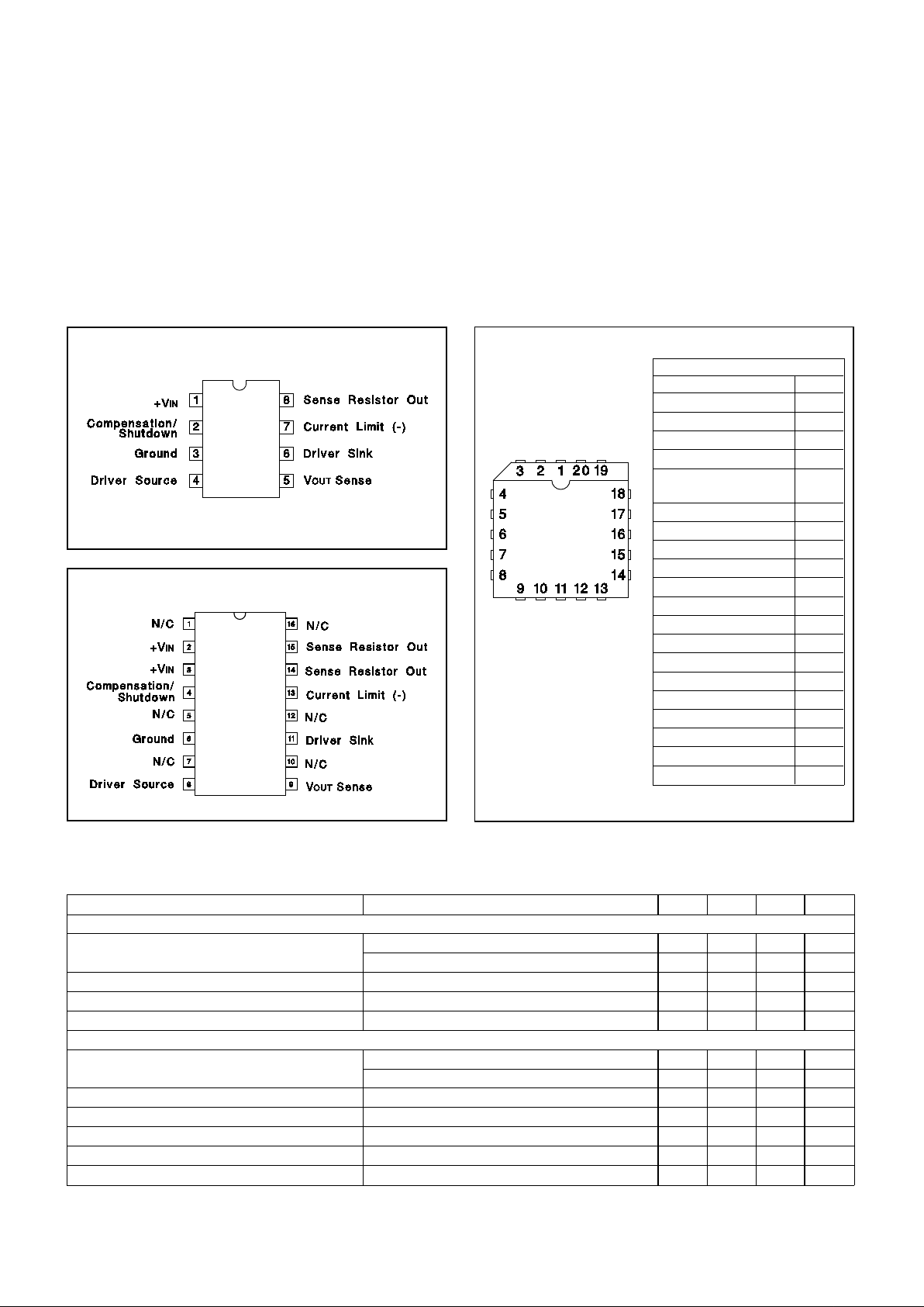
SOIC-16 (TOP VIEW)
DW Package
CONNECTION DIAGRAMS
PACKAGE PIN FUNCTION
FUNCTION PIN
N/C 1
+V
IN 2
+V
IN 3
N/C 4
Compensation/
Shutdown
5
N/C 6
Ground 7
N/C 8
N/C 9
Driver Source 10
N/C 11
V
OUT Sense 12
N/C 13
N/C 14
Driver Sink 15
N/C 16
Current Limit (-) 17
N/C 18
Sense Res isto r Out 19
Sense Res isto r Out 20
DIL-8, SOIC-8 (TOP VIEW)
N or J Package, D Package
PLCC-20, LCC-20
(TOP VIEW)
Q, L Packages
Input Supply Volt age ( +VIN) . . . . . . . . . . . . . . . . –1.0V to + 40V
Driver Outp ut Current (Sink or Source) . . . . . . . . . . . . . 600mA
Driver Sourc e to Sink Voltag e . . . . . . . . . . . . . . . . . . . . . + 40V
Maximum Curren t Throu gh Sens e Resist or. . . . . . . . . . . . . . 4A
V
OUT Sense Input Voltage . . . . . . . . . . . . . . . . . . –.3V to + 40V
Power Dissipation at T
A = 25°C (Note 2) . . . . . . . . . . . 1000mW
Power Dissipation at T
C = 25°C (Note 2). . . . . . . . . . . 2000mW
Operating Junct ion Te mp era tu re. . . . . . . . . . . -55°C to +150°C
Storage Temperature. . . . . . . . . . . . . . . . . . . . -65°C to +150°C
Lead Tempera tu re (Solderin g, 10 Seconds). . . . . . . . . . 300°C
Note 1: Voltages are refer ence d to grou nd, (Pin 3). Curre nt s are
positive into, negat ive ou t of, th e specified t er mina ls.
Consult Packaging Section of Datab ook for therma l
consideration s and limit ations of pac kage s.
ELECTRICAL CHARACTERISTICS:
Unless other wise stat ed, spe cifica tion s hold for TA = 0°C to + 70°C for the
UC3835/6, –25°C to + 85°C for the UC2835/6 , and –55°C to +12 5°C for the
UC1835/6, +V
IN = 6V, Driver Source= 0V, Drive r Sink = 5V, TA = TJ.
PARAMETER TEST CONDITIONS MIN. TYP. MAX. UNITS
Input Supply
Supply Current +V
IN = 6V 2.75 4.0 mA
+V
IN = 40V 3.75 6.0 mA
UVLO Threshold +V
IN Low to High, VOUT Sen se = 0 V 3.9 4.4 4.9 V
Threshold Hyster esis 0.1 0.35 V
Reverse Current +V
IN = -1.0V, Driver Sink Open 6.0 20 mA
Regulating Voltage an d Err or Ampl ifier (UC1835 Family Only)
Regulating Level at V
OUT Sense (VREG) Driver Current = 10mA, TJ = 25 ° C 4.94 5.0 5.06 V
Over Temperature 4.9 5.1 V
Line Regulation +V
IN = 5.2V + 35V 15 40 mV
Load Regulation Driver Current = 0 to 250mA 6. 0 25 mV
Bias Current at V
OUT Sense VOUT Sense = 5. 0 V 75 125 210 µA
Error Amp Transconductance ±100µA at Compensation/ Shut do wn P in 0.8 1.3 2.0 mS
Maximum Comp ensa tion Outp ut Current Sink or Source, Driver Source Open 90 200 260 µ A
ABSOLUTE MAXI MUM RATING S (Note 1)
2
UC1835 UC1836
UC2835 UC2836
UC3835 UC3836
PARAMETER TEST CONDITIONS MIN. TYP. MAX. UNITS
Regulating Voltage an d Err or Ampl ifier ( UC183 6 Family Only)
Regulating Level at V
OUT Sense (V REG) Driver Current = 10mA, TJ = 25°C 2.47 2.5 2.53 V
Over Temperature 2.45 2.55 V
Line Regulation +V
IN = 5.2V to 35 V 6.0 20 mV
Load Regulation Driver Current = 0 to 250mA 3. 0 15 mV
Bias Current at V
OUT Sense VOUT Sense =2.5V -1.0 -0.2 µA
Error Amp Transconductance ±100µA at Compensation/ Shut do wn P in 0.8 1.3 2.0 mS
Maximum Comp ensa tion Outp ut Current Sink or Source, Driver Source Open 90 200 260 µ A
Driver
Maximum Current 250 500 mA
Saturation Voltage Driver Current = 250 mA, Driver Sink 2.0 2.8 V
Pull-Up Current at Driver Sink Compensation/Shutdown=0.45V 140 250 300 µ A
Driver Sink Leakage In UVLO 10 µA
In Reverse Voltage (UC1835 Fam ily Only) 10 µA
Thermal Shutdown 165 °C
Foldback Cur re nt Lim i t
Current Limit Levels at Sense Resist or Out V
OUT Sense = (0 .99) VREG 2.2 2.5 2.8 A
V
OUT Sense = (0 .5 ) V REG 1.3 1.5 1.7 A
V
OUT Sense = 0V 0.25 0.4 0.55 A
Current Limit Amp Tan scon duct a n ce ±100µA at Com pen sat ion/ Shut do wn,
V
OUT Sense = (0.9) V REG
12 24 42 mS
Limiting Voltage at Curre nt Limit (-)
(Note 2)
V
OUT Sense = (0. 9) VREG
Volts Below +VIN, TJ = 25°C
80 100 140 mV
Sense Resistor Valu e (Note 3) V
OUT
Sense = (0 .9 ) V REG,
IOUT = IA, TJ = 25°C
40 mΩ
Note 2: This voltage has a positive tem per atur e coef f icient of appr oxim ately 3500 ppm / °C.
Note 3: This resistance has a positive t emperature coeff icient of appr oxim at ely 3500 ppm /°C.
The total resista nce fro m Pin 1 to Pin 8 will include an ad dition al 60 to 100m
Ω
of package resistance.
ELECTRICAL CHARACTERISTICS:
Unless other wise stat ed, spe cifica tion s hold for TA = 0°C to + 70°C for the
UC3835/6, –25°C to + 85°C for the UC2835/6 , and –55°C to +12 5°C for the
UC1835/6, +V
IN = 6V, Driver Source= 0V, Drive r Sink = 5V, TA = TJ.
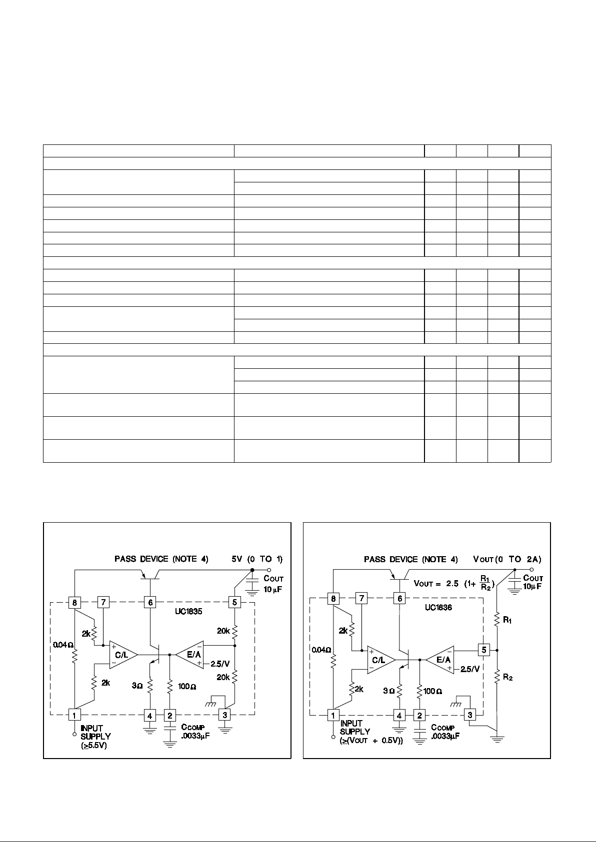
UC 1835 − Typical configurations for a 2A,
Low Dropout 5V Regul ato r
UC1836 − Typical Con fi gurati o n for a 2A,
Low Dropout Adju stab le Reg ulato r
Note 4: Suggested Pass devices are TIP 32B. (Dropout Voltage ≤0.75V) or, D45H, (Dropout V oltage ≤0.5V), or equivalents.
APPLICATION AND OPE RATI ON INFO RMATI ON
3
UC1835 UC1836
UC2835 UC2836
UC3835 UC3836
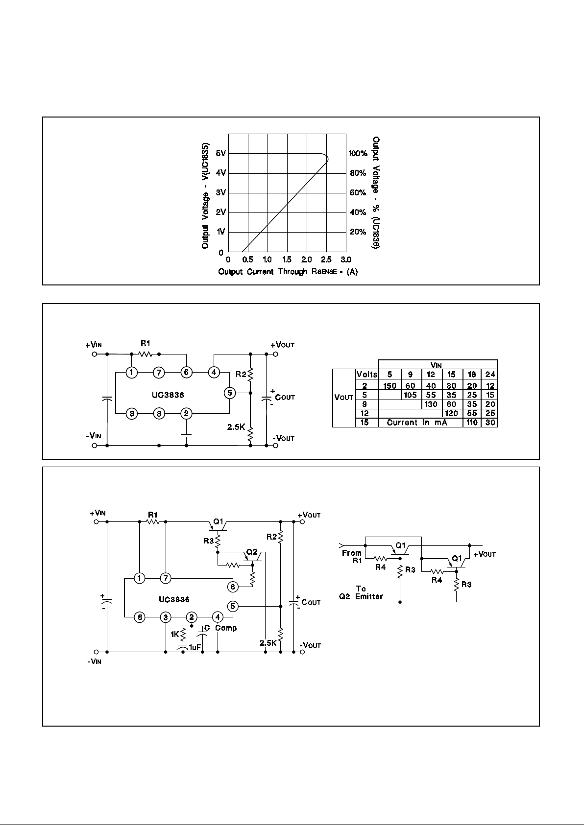
EQUATIONS:
R
1 = 0.100 V/IOUT (MAX)
R
2 = (VOUT - 2.5V/1mA)
R
3 = ((VIN - V BE - VSAT)*BETA(min))/IOUT
(max)
UC3835/36 TYPICAL APPLICATIONS
Low Current Application
using the UC3836 internal drive trans isto r
T yp i cal Outp u t Current vs V IN and VOUT
of the UC3836 intern al drive t ransist or
for P
DISS = 0.5W (ap prox.)
High Current Applicati on
using drive transist or Q 2 to increas e Q 1 base drive
and reduce UC3836 po wer diss ip at ion
Parallel Pass Transisto rs
can be added for high current or
high power dissipation applications
UNITRODE INTEGRATED CIRCUITS
7 CONTINENTAL BLVD. • MERRIMACK, NH 03054
TEL. (603) 424-2410 • FAX 603-424-3460
APPLICATION AND OPE RATI ON INFO RMATI ON (cont. )
UC1835/6 Foldback Current Limitin g
4

IMPORTANT NOTICE
T exas Instruments and its subsidiaries (TI) reserve the right to make changes to their products or to discontinue
any product or service without notice, and advise customers to obtain the latest version of relevant information
to verify, before placing orders, that information being relied on is current and complete. All products are sold
subject to the terms and conditions of sale supplied at the time of order acknowledgement, including those
pertaining to warranty, patent infringement, and limitation of liability.
TI warrants performance of its semiconductor products to the specifications applicable at the time of sale in
accordance with TI’s standard warranty. Testing and other quality control techniques are utilized to the extent
TI deems necessary to support this warranty. Specific testing of all parameters of each device is not necessarily
performed, except those mandated by government requirements.
CERT AIN APPLICATIONS USING SEMICONDUCTOR PRODUCTS MAY INVOLVE POTENTIAL RISKS OF
DEATH, PERSONAL INJURY, OR SEVERE PROPERTY OR ENVIRONMENTAL DAMAGE (“CRITICAL
APPLICATIONS”). TI SEMICONDUCTOR PRODUCTS ARE NOT DESIGNED, AUTHORIZED, OR
WARRANTED TO BE SUITABLE FOR USE IN LIFE-SUPPORT DEVICES OR SYSTEMS OR OTHER
CRITICAL APPLICATIONS. INCLUSION OF TI PRODUCTS IN SUCH APPLICA TIONS IS UNDERSTOOD T O
BE FULLY AT THE CUSTOMER’S RISK.
In order to minimize risks associated with the customer’s applications, adequate design and operating
safeguards must be provided by the customer to minimize inherent or procedural hazards.
TI assumes no liability for applications assistance or customer product design. TI does not warrant or represent
that any license, either express or implied, is granted under any patent right, copyright, mask work right, or other
intellectual property right of TI covering or relating to any combination, machine, or process in which such
semiconductor products or services might be or are used. TI’s publication of information regarding any third
party’s products or services does not constitute TI’s approval, warranty or endorsement thereof.
Copyright 1999, Texas Instruments Incorporated
 Loading...