6/94
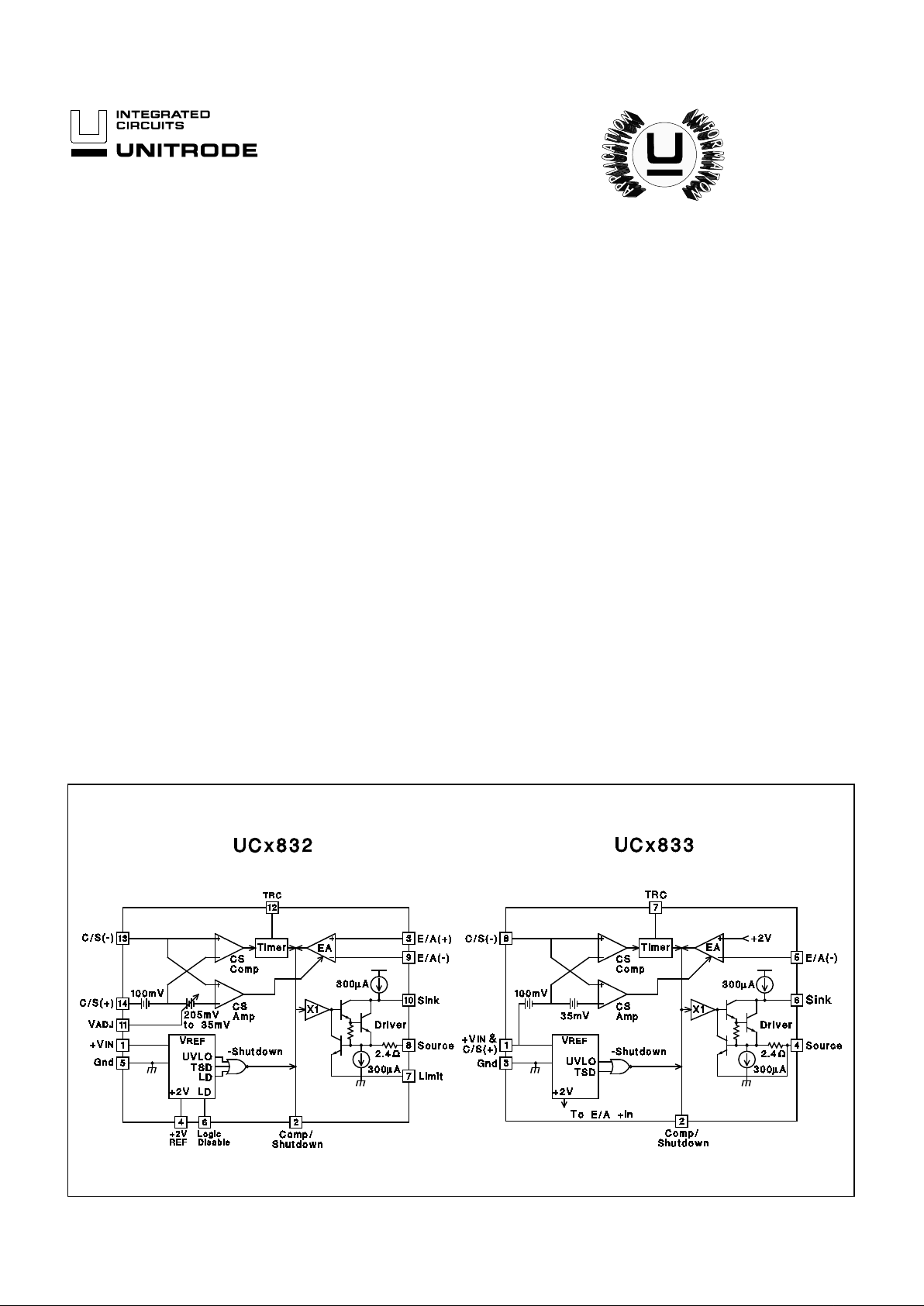
BLOCK DIAGRAMS
• Precision 1% Reference
• Over-Current Sense Threshold
Accurate to 5%
• Programmable Duty-Ratio
Over-Current Protection
• 4.5V to 36V Operation
• 100mA Output Drive, Source or
Sink
• Under-Voltage Lockout
Additional Features of the UC1832
series:
• Adjustable Current Limit to
Current Sense Ratio
• Separate +V
IN terminal
• Programmable Driver Current
Limit
• Access to V
REF
and E/A(+)
• Logic-Level Disable Input
The UC1832 a nd UC18 33 series of precisio n line ar regulato rs includ e all the
control functions re quired in the design o f very low dropout linear regulators.
Additionally, they feature an innovative duty-ratio current limiting technique
which provides peak load capab ility while limiting the average power dissipation of the external pass transistor during fault conditions. When the load current reaches an accurately programmed threshold, a gated-astable timer is
enabled, which switches the regulator’s pass device off and on at an externally
programmable duty-ratio. During the on-time of the pass element, the output
current is limited to a value slightly higher than the trip threshold of the duty-ratio timer. The constant-current-limit is programmable on the UCx832 to allow
higher peak current during the on-time of the pass device. With duty-ratio control, high initial load demands and short circuit protection may both be accommodated without extra heat sinki ng or foldback current limiting. Additionally, if
the timer pin is grounded, the du ty-ratio timer is disabled, and the IC operates
in constant-voltage/constant-current regulating mode.
These IC’s include a 2 Volt (±1%) reference, error amplifier, UVLO, and a high
current driver that has both source and sink outputs, allowing the use of either
NPN or PNP external pass transistors. Safe operation is assured by the inclusion of under-voltage lockout (UVLO) and thermal shutdown.
The UC1833 family includes the basic functions of this design in a low-cost, 8pin mini-di p package , whi le the UC 1832 seri es provides added versatility with
the availability o f 14 pins. Packagi ng options include plastic (N suffix), or ceramic (J suffix). Specified opera ting tempe rature ranges are: commercial (0°C
to 70°C), order UC3832/3 (N or J); industrial (–25°C to 85°C), order UC2832/3
(N or J); and military (–55°C to 125°C), order UC1832/3J. Surface mount
packaging is also available.
UC1832/3
UC2832/3
UC3832/3
Precision Low Dropout Linear Controllers
FEATURES DESCRIPTION
UDG-92040

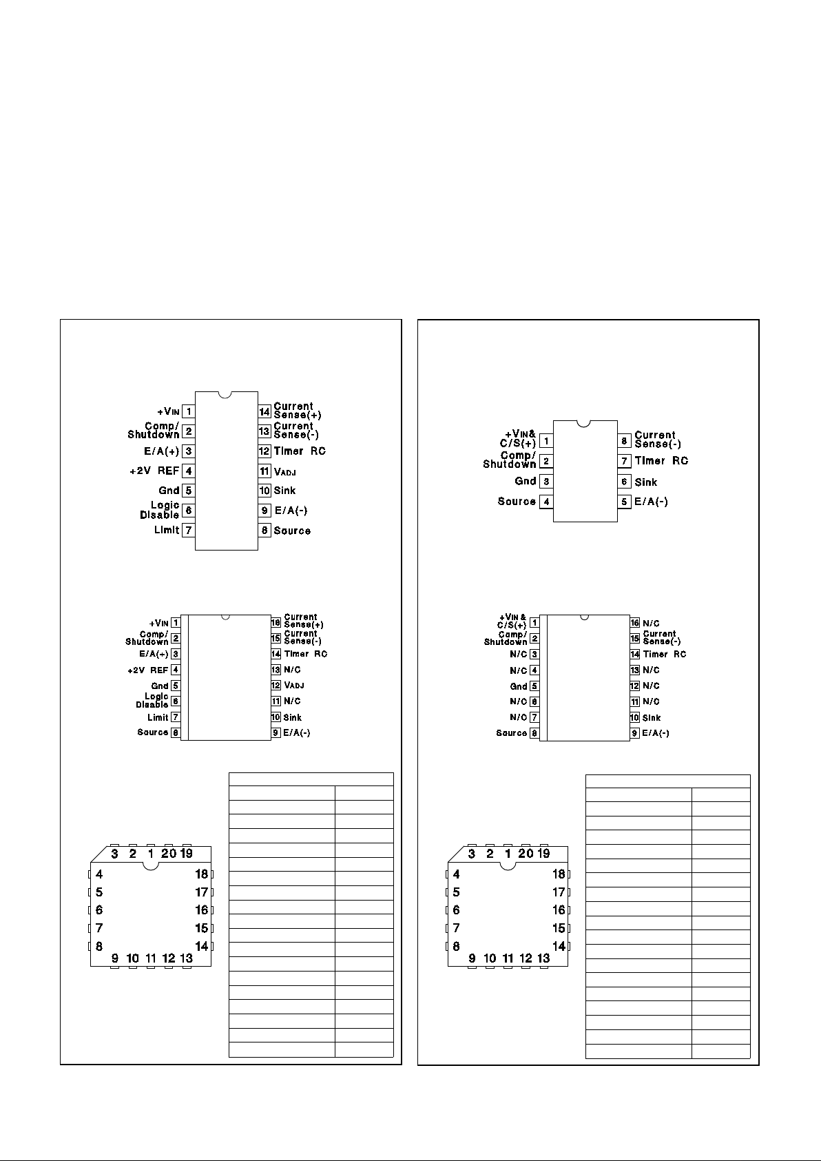
CONNECTION DIAG RAMS
DIL-14 (Top Vi ew )
J Or N Package
SOIC-16 (Top View)
DW Package
UC1832/3
UC2832/3
UC3832/3
PACKAGE PIN FUNCTION
FUNCTION PIN
N/C 1
+V
IN 2
Comp/Shutdown 3
E/A(+) 4
+2V REF 5
N/C 6
Gnd 7
Logic Disable 8
Limit 9
Source 10
N/C 11
E/A(-) 12
Sink 13
V
ADJ 14
N/C 15-17
Timer RC 18
Current Sense(- ) 19
Current Sense(+) 20
LCC-20 & PLCC-20
L & Q Package
(Top View)
ABSOLUTE MAXIMUM RATINGS
Supply Voltage +VIN. . . . . . . . . . . . . . . . . . . . . . . . . . . . . . . 40V
Driver Output Curren t (S ink or Source) . . . . . . . . . . . . . 450mA
Driver Sink to Source Voltage . . . . . . . . . . . . . . . . . . . . . . . 40V
TRC Pin Voltage. . . . . . . . . . . . . . . . . . . . . . . . . . –0. 3V to 3.2V
Other Input Vol tages. . . . . . . . . . . . . . . . . . . . . . . –0.3V t o +V
IN
Operating Jun ctio n Tem per atur e (no te 2) . . . –55°C to +150° C
Storage Temperature. . . . . . . . . . . . . . . . . . . –65°C to +150°C
Lead Temperat ure (Solde ring, 10 Sec onds ) . . . . . . . . . . 300°C
Note 1: Unless otherwise indica te d, voltages ar e re feren ced t o
ground and curre nts are posit ive into , negat ive out of, the specified terminals.
Note 2: See Unitrod e Inte gra ted C ircuit s datab ook f or
information regar ding t her m al specif icat ions an d limita tion s of
packages.
UC1832 UC1833
PACKAGE PIN FUNCTION
FUNCTION PIN
+VIN & C/S(+) 1
N/C 2
N/C 3
N/C 4
Comp/Shutdown 5
Gnd 6
N/C 7
N/C 8
N/C 9
Source 10
N/C 11
E/A(-) 12
N/C 13
N/C 14
Sink 15
Timer RC 16
Current Sense(+) 17
N/C 18-2 0
SOIC-16 (Top View)
DW Package
DIL-8 (Top View)
J Or N Package
LCC-20 & PLCC-20
L & Q Package
(Top View)
2

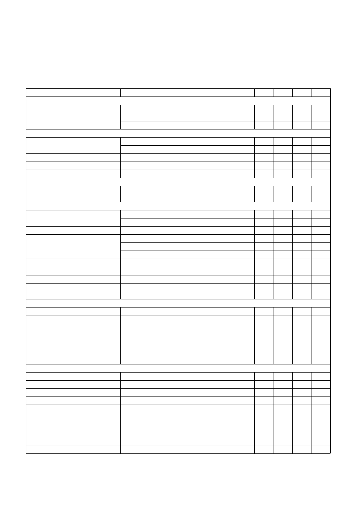
PARAMETER TEST CONDITIONS MIN TYP MAX UNITS
Input S u p pl y
Supply Curren t +V
IN = 6V 6.5 10 mA
+V
IN = 36V 9.5 15 mA
Logic Disable = 2V (UCx832 only) 3.3 mA
Reference Sect ion
Output Volta g e (Not e 3) T
J = 25°C, I DRIVER = 10mA 1.98 2.00 2.02 V
over temperature, I
DRIVER = 10mA 1.96 2.00 2.04 V
Load Regulat io n (UCx8 32 only) I
OUT = 0 to 10mA -10 -5.0 mV
Line Regulation +VIN = 4.5 to 36V, IDRIVER = 10mA 0.033 0.5 mV/V
Under-Voltage Lockout Threshold 3.6 4 .5 V
Logic Disabl e I npu t (UCx 832 on ly )
Threshold Volt age 1.3 1.4 1.5 V
Input Bias Current Logic Disable = 0V -5.0 -1.0 µA
Current Sense Section
Comparator Offset 95 100 105 mV
Over Temperature 93 100 107 mV
Amplifier Offset (UCx833 only) 110 135 170 mV
Amplifier Offset (UCx832 only) V
ADJ = Open 110 135 170 mV
V
ADJ = 1V 180 235 290 mV
V
ADJ = 0V 250 305 360 mV
Input Bias Current V
CM = +VIN 65 100 135 µA
Input Offset Current (UCx832 only) V
CM = +VIN -10 10 µA
Amplifier CMRR (UCx83 2 only) V
CM = 4.1V to +VIN+0.3V 80 dB
Transcon ductance I
COMP =
±
100µA65mS
VADJ Input Current (UCx832 only) VADJ = 0V -10 -1 µA
Timer
Inactive Leakage Current C/S(+) = C/S(-) = +V
IN; TRC pin = 2V 0.25 1.0 µA
Active Pullup Current C/S(+) = +V
IN, C/S(-) = +VIN - 0.4V; TRC pin = 0V -345 -270 -175 µA
Duty Ratio (not e 4) ontime/period , R
T = 200k, C T = 0.27µ F4.8 %
Period (not es 4, 5) ontime + offtime, R
T = 200k, CT = 0.27 µF 36 ms
Upper Trip Thr esh old (Vu) 1.8 V
Lower Trip Thresh old (Vl) 0.9 V
Trip Thresh old Rat io Vu/Vl 2.0 V/V
Error Amplifi er
Input Offset Voltage (UCx832 only) V
CM = VCOMP = 2 V -8.0 8.0 mV
Input Bias Current V
CM = VCOMP = 2 V -4.5 -1.1 µA
Input Offset Current (UCx832 only) V
CM = VCOMP = 2 V -1.5 1.5 µA
AVOL V
COMP = 1V to 13V 50 70 dB
CMRR (UCx832 only) V
CM = 0V to +VIN - 3V 60 80 dB
PSRR (UCx832 only) V
CM = 2V, +VIN = 4.5 to 36V 90 dB
Transcon duct ance ICOMP = ±10µA4.3mS
VOH I
COMP = 0, Volts below +V IN .95 1.3 V
VOL I
COMP = 0 .45 0.7 V
IOH V
COMP = 2V -700 -500 -100 µA
UC1832/3
UC2832/3
UC3832/3
Unless otherwise stated, specifications hold for TA = 0°C to 70°C for the
UC3832/3, –25°C to 85°C for the UC2832/3, and –55°C to 125°C for the
UC1832/3, +VIN = 15V, Driver sink = +V IN, C/S(+) voltage = +VIN. TA=TJ.
ELECTRICAL CHARACTERISTICS:
3
 Loading...