

Buck Current/Voltage Fed Push-Pull PWM Controllers
UC1827-1/-2
UC2827-1/-2
UC3827-1/-2
FEATURES
• Ideal for Multiple Output and/or High
Voltage Output Voltage Converters
• Up to 500kHz Operation
• High Voltage, High Current Floating
Driver for Buck Converter Stage
• UC3827-1 Current Fed Controller has
Push-Pull Drivers with Overlapping
Conduction Periods
• UC3827-2 Voltage Fed Controller has
Push-Pull Drivers with
Non-overlapping Conduction Periods
• Average Current Mode, Peak Current
Mode or Voltage Mode with Input
Voltage Feedforward Control for Buck
Power Stage
• Wide Bandwidth, Low Offset,
Differential Current Sense Amplifier
• Precise Short Circuit Current Control
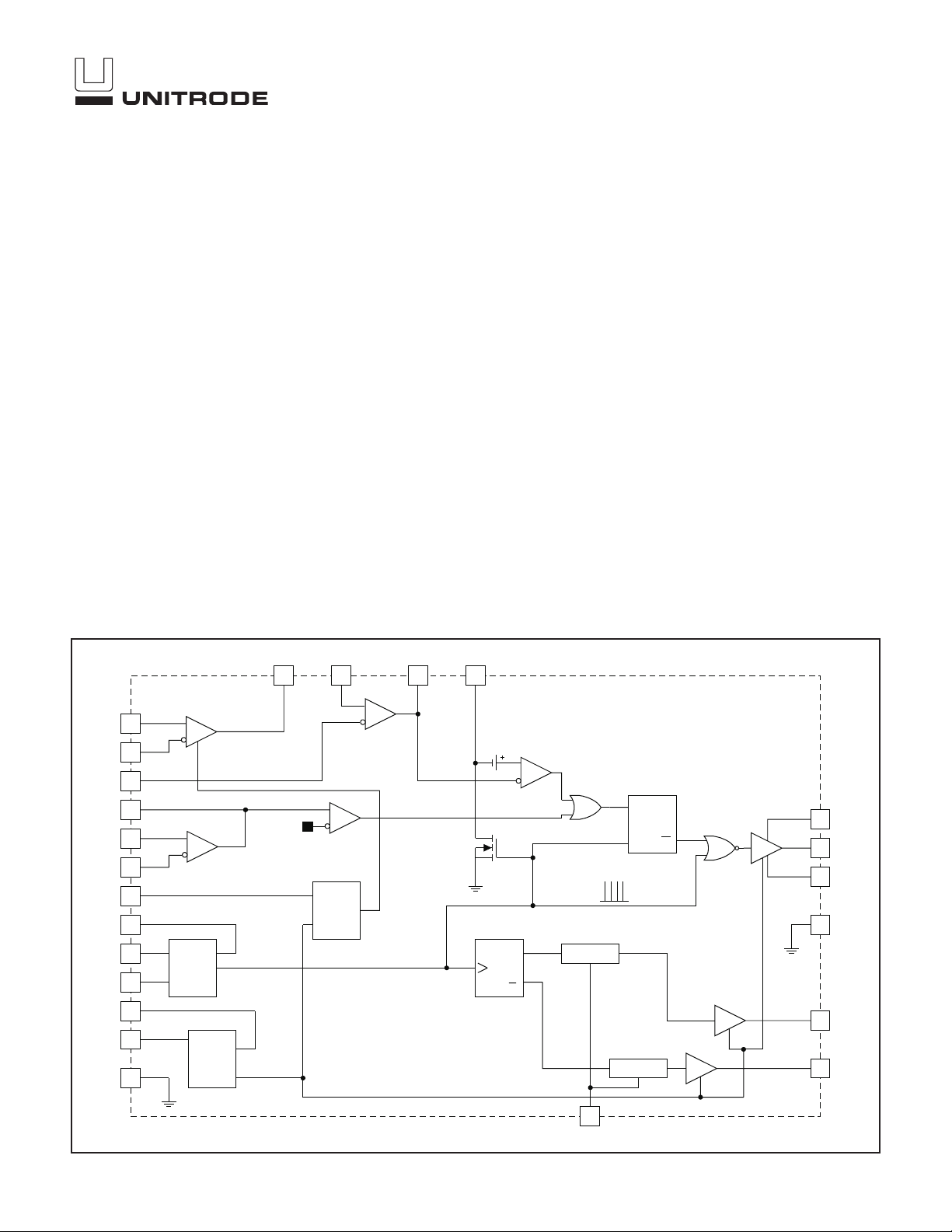
BLOCK DIAGRAM
DESCRIPTION
The UC3827 family of controller ICs provides an integrated control solution
for cascaded buck and push-pull converters. These converters are known
as current fed or voltage fed push-pull converters and are ideally suited for
multiple output and/or high voltage output applications. In both current fed
and voltage fed modes, the push-pull switches are driven at 50% nominal
duty cycles and at one half the switching frequency of the buck stage. In
the current fed mode, the two switches are driven with a guaranteed overlap period to prevent ringing and voltage stress on the devices. In the voltage fed mode, the two switches are driven with a guaranteed gap time
between the switches to prevent shorting the transformer across the energy storage capacitor and to prohibit excessive currents flowing through
the devices.
The converter’s output voltage is regulated by pulse width modulation of
the buck switch. The UC3827 contains complete protection and PWM control functions for the buck converter. Easy control of the floating switch is
accomplished by the floating drive circuitry. The gate drive waveform is
level shifted to support an input voltage up to 72Vdc.
(continued)
VEA+
VEA–
CEA–
CSAO
CSA+
CSA–
SS
SYNC 19
CT
RT
REF
VCC
GND
14
16
13
7
8
9
4
18
17
15
23
11
VOLTAGE ERROR
AMPLIFIER
CURRENT
SENSE AMPLIFIER
OSC
500kHz
MAX
REF
&
UVLO
UVLO
10
+3V
ILIM
COMPARATOR
SS
UV
12
CURRENT
ERROR
AMPLIFIER
INHBT
CEAOVEAO
6 5
RAMPCEA+
0.7V
PWM
COMPARATOR
T
R
D
QS
OSC
Q
Q
DELAY
DELAY
FLYING
DRIVER
PUSH-PULL
DRIVERS
1
V+
2
BUCK
3
SRC
21
PGND
24
PUSH
22
PULL
04/99
20
DELAY
UDG-97172
DESCRIPTION (cont.)
The UC3827 can be set up in traditional voltage mode
control using input voltage feedforward technique or in
current mode control. Using current mode control prevents
potential core saturation of the push-pull transformer due
to mismatches in timing and in component tolerances.
With average current mode control, precise control of the
inductor current feeding the push-pull stage is possible
without the noise sensitivity associated with peak current
mode control. The UC3827 average current mode loop
can also be connected in parallel with the voltage regulation loop to assist only in fault conditions.
Other valuable features of the UC3827 include
bidirectional synchronization capability, user programmable overlap time (UC3827-1), user programmable gap
time (UC3827-2), a high bandwidth differential current
sense amplifier, and soft start circuitry.
ABSOLUTE MAXIMUM RATINGS
Supply Voltage, VCC. . . . . . . . . . . . . . . . . . . . . . . . . . . . . . 20V
Input Voltage Range
For all pins except V+, BUCK, SRC. . . . . . . . . . –0.3V to 5V
For V+ and BUCK. . . . . . . . . . . . . . . . . . . . . . . . . . . . . . 90V
For SRC . . . . . . . . . . . . . . . . . . . . . . . . . . . . . . . . 90V–VCC
BUCK Driver
IO Continuous. . . . . . . . . . . . . . . . . . . . . . . . . . . . . ± 250mA
IO Peak . . . . . . . . . . . . . . . . . . . . . . . . . . . . . . . . . . . . . ± 1A
PUSH/PULL Driver
IO Continuous. . . . . . . . . . . . . . . . . . . . . . . . . . . . . ± 200mA
IO Peak. . . . . . . . . . . . . . . . . . . . . . . . . . . . . . . . . . . . ± 0.8A
Storage Temperature . . . . . . . . . . . . . . . . . . . −65°C to +150°C
Junction Temperature. . . . . . . . . . . . . . . . . . . –55°C to +150°C
Lead Temperature (Soldering, 10 sec.). . . . . . . . . . . . . +300°C
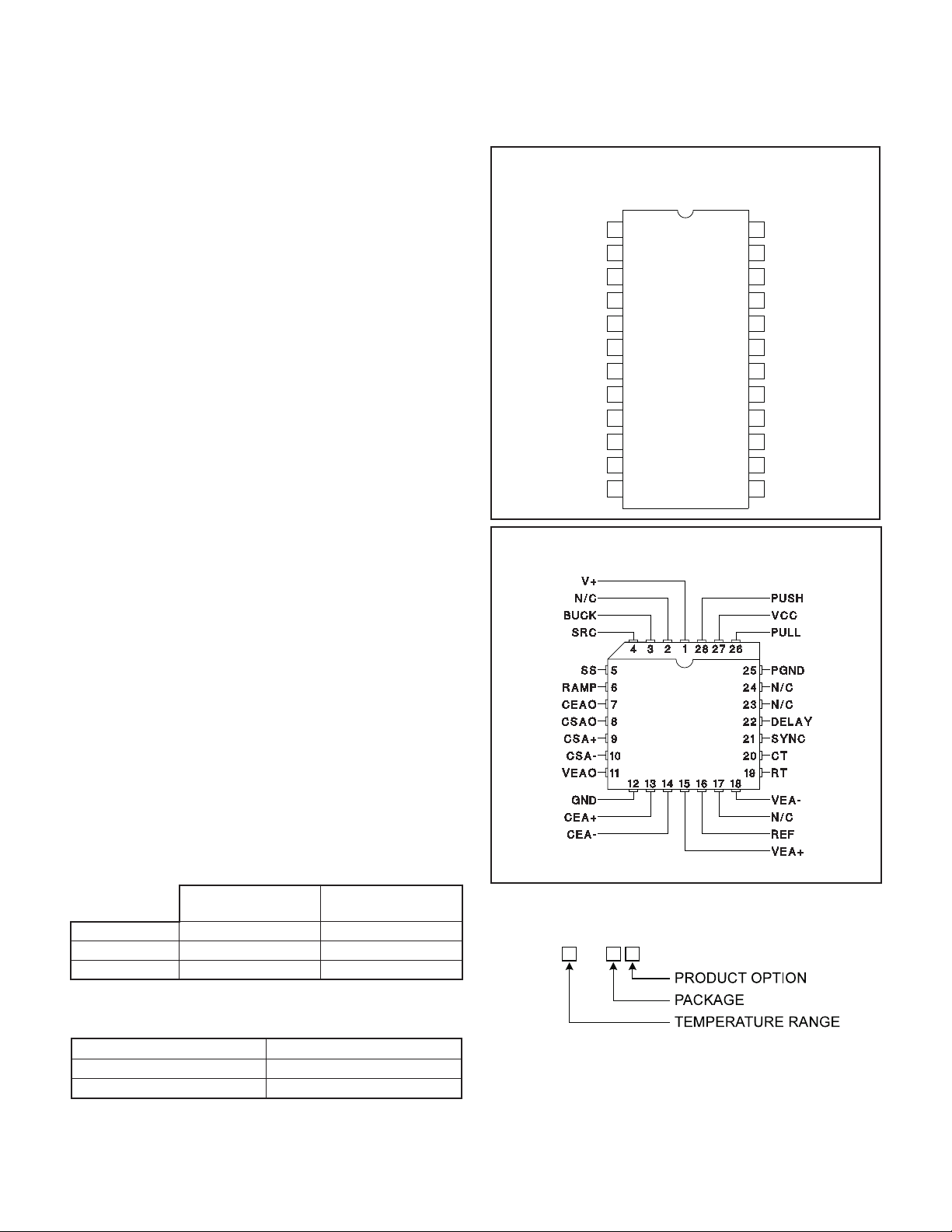
CONNECTION DIAGRAMS
DIL-24 (Top View)
N or J, DW Packages
V+
1
2
BUCK
SRC
3
4
SS
5
RAMP
6
CEAO
7
CSAO
8
CSA+
9
CSA–
VEAO
10
11
GND
12
CEA+ CEA–
PLCC-28 (Top View)
Q Package
UC1827-1/-2
UC2827-1/-2
UC3827-1/-2
24
PUSH
VCC
23
PULL
22
PGND
21
DELAY
20
SYNC
19
CT
18
RT
17
VEA–
16
15
REF
1413VEA+
Voltages are referenced to ground. Currents are positive into,
negative out of the specified terminal. Consult Packaging
Section of Databook for thermal limitations and considerations
of packages.
TEMPERATURE AND PACKAGE
SELECTION GUIDE
TEMPERATURE
RANGE
UC1827-X –55°C to +125°C J
UC2827-X –40°C to +85°C N, DW, Q
UC3827-X 0°C to +70°C N, DW, Q
AVAILABLE
PACKAGES
PART VERSION GUIDE
PART NUMBER TOPOLOGY
UCX827-1 Current Fed Push-Pull
UCX827-2 Voltage Fed Push-Pull
ORDERING INFORMATION
UC 827
2
UC1827-1/-2
UC2827-1/-2
UC3827-1/-2
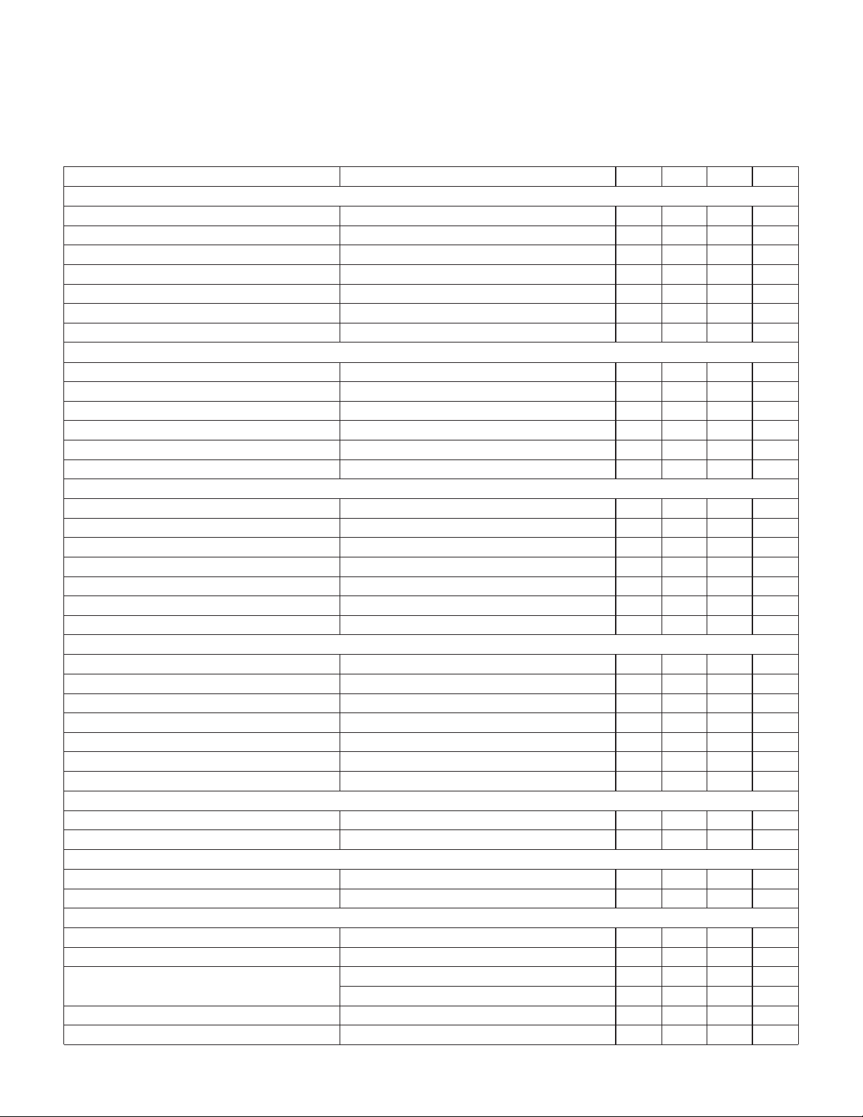
ELECTRICAL CHARACTERISTICS
Unless otherwise specified, VCC = 15V, V+ = 14.3V, CT = 340pF, RT = 10K,
RDELAY = 24.3k, SRC = GND, BUCK, PUSH and PULL outputs no load. TJ = TA.
PARAMETER TEST CONDITIONS MIN TYP MAX UNITS
Supply
VCC UVLO, Turn-On 8.3 8.8 9.5 V
Hysteresis 0.9 1.2 1.5 V
I
Start VCC = 8V 1000 µA
VCC
I
Run 32 45 mA
VCC
V+ UVLO, Turn-On 7.1 7.5 8.3 V
V+ Hysteresis 0.2 0.4 0.9 V
I
+
Buck High 0.2 1 2 mA
V
Voltage Error Amplifier
IB 0.5 3 µA
VIO 10 mV
AVOL 80 95 dB
GBW (Note 7) 1 4 MHz
VOL I
VOH I
= 0µA (No Load) 0.3 0.5 V
VEAO
= 0µA (No Load) 2.85 3 3.20 V
VEAO
Current Sense Amplifier
IB –1 –5 uA
VIO 5mV
AVOL 80 110 dB
GBW (Note 7) 15 29 MHz
VOL I
VOH I
= 0µA (No Load) 0.25 0.5 V
CEAO
= 0µA (No Load) 3 3.3 V
CEAO
Common Mode Range (Note 7) 0 2 V
Current Error Amplifier
IB –1 –5 µA
VIO 10 mV
AVOL 80 110 dB
GBW At 100kHz, Measure Gain 2 4.5 MHz
VOL I
VOH I
= 0µA (No Load) 0.25 0.5 V
CEAO
= 0µA (No Load) 3.3 3.5 V
CEAO
Common Mode Range (Note 7) 0 5 V
Oscillator Section
Frequency 180 220 250 kHz
CT Discharge Current 3.5V at CT when CT removed 5 mA
PWM Comparator
Minimum Duty Cycle 200kHz 0 %
Maximum Duty Cycle 200kHz 85 91 95 %
Buck Output Stage
Rise Time 1nF Load, (Note 3) 40 100 ns
Fall Time 1nF, Load 30 80 ns
VOH I
VOL I
= –15mA , V+ –BUCK (Note 4) 1.5 2.5 V
BUCK
I
= –150mA, V+ – BUCK (Note 4) 2 2.5 V
BUCK
= 15mA (Note 5) 0.2 0.4 V
BUCK
I
= 150mA (Note 5) 0.7 1.2 V
BUCK
3

UC1827-1/-2
UC2827-1/-2
UC3827-1/-2
ELECTRICAL CHARACTERISTICS Unless otherwise specified, VCC = 15V, V+ = 14.3V, CT = 340pF, RT = 10K,
RDELAY = 24.3k, SRC = GND, BUCK, PUSH and PULL outputs no load. TJ = TA.
PARAMETER TEST CONDITIONS MIN TYP MAX UNITS
Push/Pull Output Stages
Rise Time 1nF Load 50 100 ns
Fall Time 1nF Load 35 100 ns
Overlap Time, -1 Only 1nF loads (Note 1) 100 250 400 ns
Non-Overlapping Time, -2 Only (Note 2) 100 250 500 ns
VOH I
VOL I
Reference
REF Voltage 4.8 5 5.2 V
Short Circuit Current REF = 0V –35 –50 –65 mA
Line Regulation 9.5V < VCC < 20V 5 20 mV
Load Regulation 0mA < IO < 10mA 8 20 mV
Soft Start
VOL, Saturation VCC = 7V 250 500 mV
I
SS –5 –12 –25 µA
Note 1: The overlap time is measured from the point at which the rising edge of PUSH/PULL crosses 5V until the falling edge of
Note 2: The non-overlap time is measured from the point at which the falling edge of PUSH/PULL crosses 5V until the rising edge
Note 3: Measure the rise time from when BUCK crosses 1V until it crosses 9V.
Note 4: To force BUCK high, force CSAO=2.5V, CEAO = 2.5V, a 25k pulldown resistor form RAMP to ground, and CT = 0.5V.
Note 5: To force BUCK low, force CSAO = 2.5V, CEAO = 2.5V, a 10k pulldown resistor from RAMP to ground, and CT = 3.5V.
Note 6: To toggle PUSH or PULL into a desired state, pulse CT from 0.5V to 3.5V. PUSH and PULL toggle on the rising edge of
Note 7: Guaranteed by design. Not 100% tested in production.
PULL/PUSH crosses 5V.
of PULL/PUSH crosses 5V.
CT.
PUSH/PULL = –10mA, VCC – PUSH (Note 6) 2 3 V
I
PUSH/PULL = –100mA, VCC – PUSH (Note 6) 2.5 3 V
PUSH/PULL = 10mA (Note 6) 0.2 0.8 V
I
PUSH/PULL = 100mA (Note 6) 0.6 1.2 V
PIN DESCRIPTIONS
BUCK: Output of the buck PWM controller. The BUCK
output is a floating driver, optimized for controlling the
gate of an N-channel MOSFET. The peak sink and
source currents are 1A. Any undervoltage faults will disable BUCK to an off condition (low).
CEA+: The non-inverting input of the current error amplifier.
CEA–: The inverting input of the current error amplifier.
CEAO: The output of the current error amplifier and the
inverting input of the PWM comparator of the buck converter.
CSA+: The noninverting input of the current sense amplifier.
CSA–: The inverting input of the current sense amplifier.
CSAO: The output of the current sense amplifier and the
noninverting input of the current limit comparator. When
the signal level on this pin exceeds the 3V threshold of
the current limit comparator, the buck gate drive pulse is
terminated. This feature is useful to implement cycle-by-cycle current limiting for the buck converter.
CT: This pin is provided for the timing capacitor which is
connected between CT and GND. The oscillator frequency is set by CT and a resistor RT, connected between pin RT and GND. The CT discharge current is
approximately 40X the bias current through the resistor
connected to RT. A practical maximum value for the discharge current is 20mA. The frequency of the oscillator is
given by:
fOSC =
0.77
RT •CT
4

PIN DESCRIPTIONS (cont.)
DELAY: A resistor to GND programs the overlap time of
the PUSH and PULL outputs of the UC3827-1 and the
dead time of the PUSH and PULL outputs of the
UC3827-2. The minimum value of the resistor, RDELAY,
is 18kΩ. The delay or overlap time is given by:
TDELAY =
GND: This pin is the ground reference for all sensitive
setup components not related to driving the outputs.
They include all timing, voltage sense, current sense,
and bypass components.
PGND: Ground connection for the PUSH and PULL outputs. PGND must be connected to GND at a single point
on the printed circuit board. This is imperative to prevent
large, high frequency switching currents flowing through
the ground metalization inside the IC.
PULL: Ground referenced output to drive an N-channel
MOSFET. The PULL and the PUSH outputs are driving
the two switches of the push-pull converter with complementary signals at close to a 50% duty cycle. Any
undervoltage faults will disable PULL to an off condition
(low).
PUSH: Ground referenced output to drive an N-channel
MOSFET. The PULL and the PUSH outputs are driving
the two switches of the push-pull converter with complementary signals at close to a 50% duty cycle. Any
undervoltage faults will disable PUSH to an off condition
(low).
RAMP: The RAMP voltage, after a 700mV internal level
shift, is fed to the noninverting input of the buck PWM
comparator.A resistor to Vin and a capacitor to GND provide an input voltage feedforward signal for the buck controller in voltage mode control. In peak current mode
control, the RAMP pin receives the current signal of the
buck converter. In an average current mode setup, the
RAMP pin has a linearly increasing ramp signal. This
waveform may be generated either by connecting RAMP
directly to CT, or by connecting both a resistor from VCC
to RAMP and a capacitor from RAMP to GND.
REF: The output of the +5V on board reference. Bypass
this pin with a capacitor to GND. The reference is off
when the chip is in undervoltage lockout mode.
RDELAY
Ω
200
–9
•10 sec.
UC1827-1/-2
UC2827-1/-2
UC3827-1/-2
REF
2•
RT
The charge current should be less than 500µAtokeep
CT’s discharge peak current less than 20mA, which is
CT’s maximum practical discharge value. The discharge
time, which sets the maximum duty cycle, is set internally
and is influenced by the charge current.
SRC: The source connection for the floating buck switch.
The voltage on the SRC pin can exceed VCC but must
be lower than 90V-VCC.Also, during turn-off transients of
the buck switch, the voltage at SRC can go to –2V.
SS: The soft start pin requires a capacitor to GND. During soft start the output of the voltage error amplifier is
clamped to the soft start capacitor voltage which is slowly
charged by an internal current source. In UVLO, SS is
held low.
SYNC: SYNC is a bidirectional pin for the oscillator. This
pin can be used to synchronize several chips to the fastest oscillator. Its input synchronization threshold is 1.4V.
The SYNC voltage is 3.6V when the oscillator capacitor,
CT, is discharged. Otherwise it is 0V. If the recommended
synchronization circuit is not used, a 1k or lower value
resistor from SYNC to GND may be needed to increase
the fall time of the signal at SYNC.
VCC: A voltage source connected to this pin supplies the
power for the UC3827. It is recommended to bypass this
pin to both GND and PGND ground connections with
good quality high frequency capacitors.
VEA+: The non-inverting input of the voltage error amplifier.
VEA–: The inverting input of the voltage error amplifier.
VEAO:The output of the voltage error amplifier.
V+: Supply voltage for the buck output.The floating driver
of the UC3827 uses the bootstrap technique which requires a reservoir capacitor to store the required energy
for the on time of the buck switch. A diode must be connected from VCC to V+ to charge the reservoir capacitor.
This diode must be able to withstand Vin. The reservoir
capacitor must be connected between V+ and SRC and
its voltage is monitored directly by the undervoltage lockout circuitry of the buck driver.
RT: A resistor to GND programs the charge current of the
timing capacitor connected to CT. The charge current approximately equals:
5
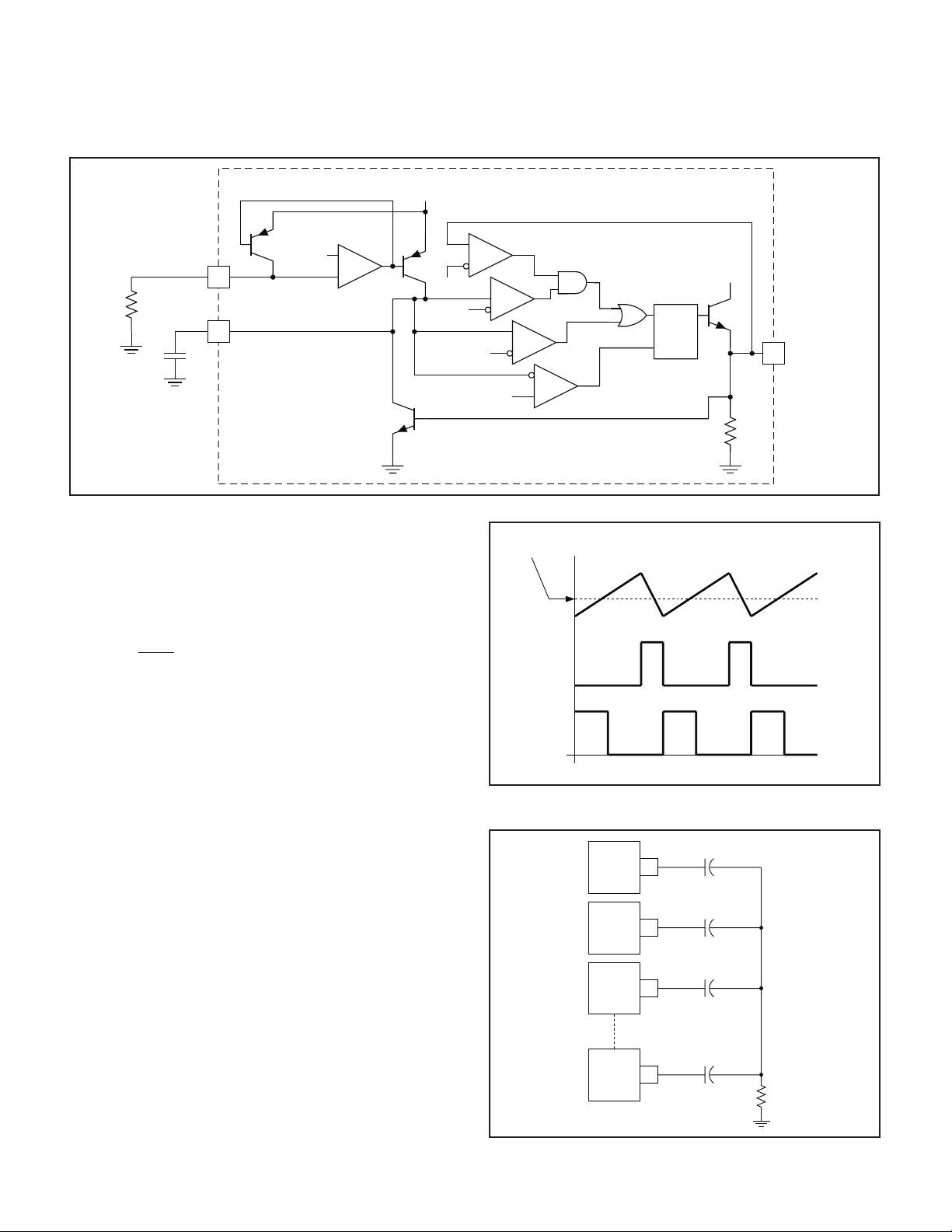
APPLICATION INFORMATION
UC1827-1/-2
UC2827-1/-2
UC3827-1/-2
V
REF
RT
CT
R
T
C
T
2.5V
–
+
1.4V
2.5V
2.9V
Figure 1. Oscillator block with external connections.
CIRCUIT BLOCK DESCRIPTION
PWM Oscillator.
nal connections is shown in Fig. 1. A resistor (R
The oscillator block diagram with exter-
) con-
T
nected to pin RT sets the linear charge current:
V
25.
I
≈
RT
R
T
The timing capacitor (C
) is linearly charged with the
T
charge current forcing the OSC pin to charge to a 3.4V
threshold. After exceeding this threshold, the RS flip-flop
is set driving CLKSYN high and RDEAD low which discharges C
. CT continues to discharge until it reaches a
T
0.5V threshold and resets the RS flip-flop which repeats
the charging sequence as shown in Fig.2.
OSCILLATOR
V
REF
S
R
0.5V
10k
VAO CURRENT
COMMAND
2.9V
0.5V
3.6V
1.4V
8.5V
0V
CHARGING
THRESHOLD
DISCHARGING
Figure 2. Oscillator and PWM output waveform.
SYNC
UDG-99087
UDG-99086
OSC
CLKSYN
OUT
As shown in Fig. 3, several oscillators are synchronized to
the highest free running frequency by connecting 100pF
capacitors in series with each CLKSYN pin and connecting the other side of the capacitors together forming the
CLKSYN bus. The CLKSYN bus is then pulled down to
ground with a resistance of approximately 10k. Referring
to Fig. 1, the synchronization threshold is 1.4V. The oscillator blanks any synchronization pulse that occurs when
OSC is below 2.5V. This allows units, once they discharge
below 2.5V, to continue through the current discharge and
subsequent charge cycles whether or not other units on
the CLKSYN bus are still synchronizing. This requires the
frequency of all free running oscillators to be within 17%
of each other to guarantee synchronization.
UNITRODE CORPORATION
7 CONTINENTAL BLVD.• MERRIMACK, NH 03054
TEL. (603) 424-2410 • FAX (603) 424-3460
100pF
OSC1
OSC2
OSC3
OSC10
SYNC
SYNC
SYNC
SYNC
100pF
100pF
CLKSYN BUS
100pF
10k
Figure 3. Oscillator synchronization connection
diagram.
6
UDG-99085

IMPORTANT NOTICE
T exas Instruments and its subsidiaries (TI) reserve the right to make changes to their products or to discontinue
any product or service without notice, and advise customers to obtain the latest version of relevant information
to verify, before placing orders, that information being relied on is current and complete. All products are sold
subject to the terms and conditions of sale supplied at the time of order acknowledgement, including those
pertaining to warranty, patent infringement, and limitation of liability.
TI warrants performance of its semiconductor products to the specifications applicable at the time of sale in
accordance with TI’s standard warranty. Testing and other quality control techniques are utilized to the extent
TI deems necessary to support this warranty . Specific testing of all parameters of each device is not necessarily
performed, except those mandated by government requirements.
CERTAIN APPLICA TIONS USING SEMICONDUCTOR PRODUCTS MA Y INVOLVE POTENTIAL RISKS OF
DEATH, PERSONAL INJURY, OR SEVERE PROPERTY OR ENVIRONMENTAL DAMAGE (“CRITICAL
APPLICATIONS”). TI SEMICONDUCTOR PRODUCTS ARE NOT DESIGNED, AUTHORIZED, OR
WARRANTED TO BE SUITABLE FOR USE IN LIFE-SUPPORT DEVICES OR SYSTEMS OR OTHER
CRITICAL APPLICA TIONS. INCLUSION OF TI PRODUCTS IN SUCH APPLICATIONS IS UNDERST OOD TO
BE FULLY AT THE CUSTOMER’S RISK.
In order to minimize risks associated with the customer’s applications, adequate design and operating
safeguards must be provided by the customer to minimize inherent or procedural hazards.
TI assumes no liability for applications assistance or customer product design. TI does not warrant or represent
that any license, either express or implied, is granted under any patent right, copyright, mask work right, or other
intellectual property right of TI covering or relating to any combination, machine, or process in which such
semiconductor products or services might be or are used. TI’s publication of information regarding any third
party’s products or services does not constitute TI’s approval, warranty or endorsement thereof.
Copyright 1999, Texas Instruments Incorporated
 Loading...