Texas Instruments UC3824N, UC3824DWTR, UC3824DW, UC2824QTR, UC2824N Datasheet
...
3/97
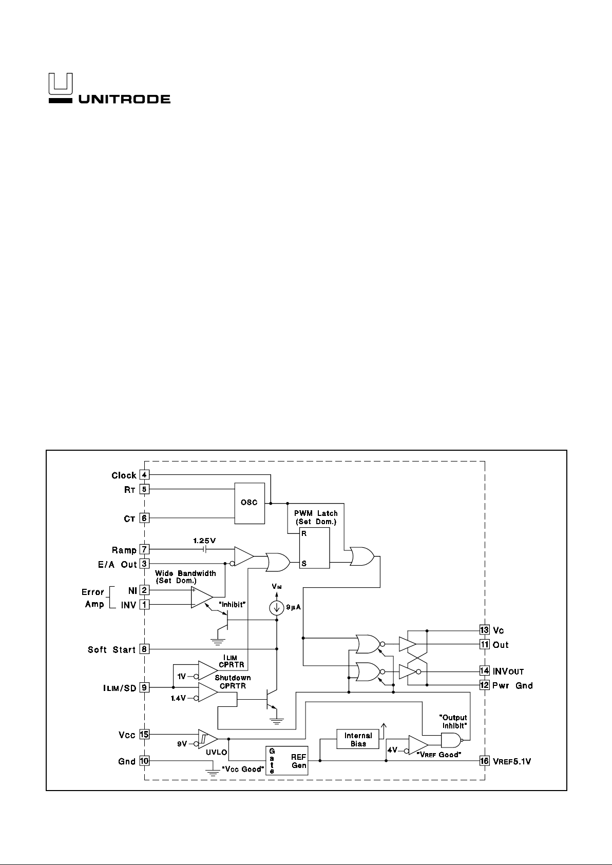
BLOCK DIAGRAM
• Complementary Outputs
• Practical Operation Switching Frequencies
to 1MHz
• 50ns Propagation Delay to Output
• High Current Dual Totem Pole Outputs
(1.5A Peak)
• Wide Bandwidth Error Amplifier
• Fully Latched Logic with Double Pulse
Suppression
• Pulse-by-Pulse Current Limiting
• Soft Start / Max. Duty Cycle Control
• Under-Voltage Lockout with Hysteresis
• Low Start Up Current (1.1 mA)
• Trimmed Bandgap Reference (5.1V ± 1%)
The UC1824 family of PWM control ICs is optimized for high frequency switched mode power supply applications. Particular care
was given to min imi zin g pr opagation delay s through the comparators
and logic c ircuitry while maximizing bandwidth and slew rate of the
error amplifier. This controller is designed for use in either currentmode or voltage mod e systems with the capability for input voltage
feed-forward.
Protection circuitry includes a current limit comparator with a 1V
threshold, a TTL compatible shutdown port, and a soft start pin which
will double as a maximum duty cycle clamp. The logic is fully latched
to provide jitter free operation and prohibit multiple pulses at an output. An under-voltage lockout secti on with 800mV of hysteresis assures low start up current. Dur ing under-voltage lockout, the outputs
are high impedance.
These devices feature totem pole outputs designed to source and
sink high peak currents from capacitive l oads, such as the gate of a
power MOSFET. The on state is designed as a high level.
UC1824
UC2824
UC3824
High Speed PWM Controller
FEATURES DESCRIPTION
UDG-92034-1

CONNECTION DIAGRAMS
DIL-16 (Top View)
J Or N Package
SOIC-16 (Top View)
DW Package
UC1824
UC2824
UC3824
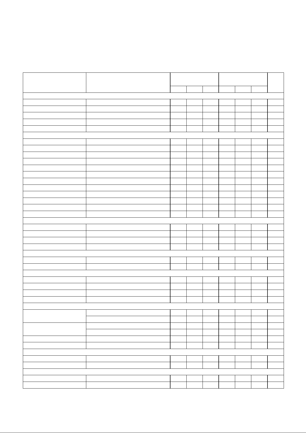
ELECTRICAL CHARACTERISTICS:
Unless otherwise st ated,these spe ci fi ca ti ons apply for , RT = 3.65k, CT = 1nF, V
CC
= 15V, -55°C<TA<125°C for the UC1824, –40°C<TA<85°C for the UC2824, and
0°C<TA<70°C for the UC3824, TA=T
J.
UC1824
UC3824
PARAMETERS TEST CONDITIONS UC2824
MIN TYP MAX MIN TYP MAX UNITS
Reference Section
Output Voltage T
J
= 25°C, IO = 1mA 5.05 5.10 5.15 5.00 5.10 5.20 V
Line Regulation 10V < V
CC
< 30V 2 20 2 20 mV
Load Regulation 1mA < I
O
< 10mA 5 20 5 20 mV
Temperature Stability* T
MIN
< TA < T
MAX
0.2 0.4 0.2 0.4 mV/°C
Total Output Variat io n* Li ne , Lo ad , Te mp era tu r e 5.00 5.20 4.95 5.25 V
Output Noise Volt ag e* 10Hz < f < 10kHz 50 50
µ
V
Long Term Stability* T
J
= 125°C, 1000hrs. 5 25 5 25 mV
Short Circuit Current V
REF
= 0V -15 -50 -100 -15 -50 -100 mA
Oscillator Section
Initial Accuracy* TJ = 25°C 360 400 440 360 400 440 k Hz
Voltage Stability* 10V < V
CC
< 30V 0.2 2 0.2 2 %
Temperature Stability* T
MIN
< TA < T
MAX
55%
Total Variation* Line, Temperature 340 460 340 460 kHz
PACKAGE PIN FUNCTION
FUNCTION
PIN
N/C 1
INV 2
NI 3
E/A Out 4
Clock 5
N/C 6
R
T
7
C
T
8
Ramp 9
Soft Start 10
N/C 11
ILIM/SD 12
Gnd 13
Out 14
Pwr Gnd 15
N/C 16
V
C
17
INV
OUT
18
V
CC
19
V
REF
5.1V 20
PLCC-20 & LCC-20
(Top View)
Q & L Packages
ABSOLUTE MAXIMUM RATINGS
(Note 1)
Supply Voltage (Pins 13, 15) . . . . . . . . . . . . . . . . . . . . . . . . 30V
Output Current, Source or Sink (Pins 11, 14)
DC. . . . . . . . . . . . . . . . . . . . . . . . . . . . . . . . . . . . . . . . . . . . 0.5A
Pulse (0.5µs) . . . . . . . . . . . . . . . . . . . . . . . . . . . . . . . . . . . 2.0A
Analog Inputs
(Pins 1, 2, 7) . . . . . . . . . . . . . . . . . . . . . . . . . . . . . . . -0.3V to 7V
(Pin 8, 9). . . . . . . . . . . . . . . . . . . . . . . . . . . . . . . . . . -0.3V to 6V
Clock Output Current (Pin 4) . . . . . . . . . . . . . . . . . . . . . . . -5mA
Error Amplifier Output Current (Pin 3) . . . . . . . . . . . . . . . . 5mA
Soft Start Sink Current (Pin 8) . . . . . . . . . . . . . . . . . . . . . 20mA
Oscillator Charging Current (Pin 5) . . . . . . . . . . . . . . . . . . -5mA
Power Dis sipation . . . . . . . . . . . . . . . . . . . . . . . . . . . . . . . . 1W
Storage Temperature Range . . . . . . . . . . . . . . -65°C to +150°C
Lead Temperature (Soldering, 10 seconds) . . . . . . . . . . 300°C
Note 1: All voltages are with respect to GND (Pin 10); all currents are positive into, negative out of part; pin numbers refer to
DIL-16 package.
Note 3: Consult Unitrode Integrated Circuit Databook for thermal limitations and considerations of package.
2

UC1824
UC3824
PARAMETERS TEST CONDITIONS UC2824
MIN TYP MAX MIN TYP MAX UNITS
Oscillator Section (cont. )
Clock Out High 3.9 4.5 3.9 4.5 V
Clock Out Low 2.3 2.9 2.3 2.9 V
Ramp Peak* 2.6 2.8 3.0 2.6 2.8 3.0 V
Ramp Valley* 0.7 1.0 1.25 0.7 1.0 1.25 V
Ramp Valley to Peak* 1.6 1.8 2.0 1.6 1.8 2.0 V
Error Amplifier Section
Input Offset Voltage 10 15 mV
Input Bias Current 0.6 3 0.6 3
µ
A
Input Offset Current 0.1 1 0.1 1
µ
A
Open Loop Gain 1V < V
O
< 4V 60 95 60 95 dB
CMRR 1.5V < V
CM
< 5.5V 75 95 75 95 dB
PSRR 10V < V
CC
< 30V 85 110 85 110 dB
Output Sink Current V
PIN 3
= 1V 12.5 12.5 mA
Output Source Current V
PIN 3
= 4V -0.5 -1.3 -0.5 -1.3 mA
Output High Voltage I
PIN 3
= -0.5mA 4.0 4.7 5.0 4.0 4.7 5.0 V
Output Low Voltage I
PIN 3
= 1mA 0 0 .5 1.0 0 0.5 1.0 V
Unity Gain Bandwidth* 35.5 35.5 MHz
Slew Rate* 612 612 V/
µ
s
PWM Comparator Section
Pin 7 Bias Current V
PIN 7
= 0V -1 -5 -1 -5
µ
A
Duty Cycle Range 0 80 0 85 %
Pin 3 Zero DC Threshold V
PIN 7
= 0V 1.1 1.25 1.1 1.25 V
Delay to Output* 50 80 50 80 ns
Soft-Start Section
Charge Current V
PIN 8
= 0.5V 3 9 20 3 9 20
µ
A
Discharge Current V
PIN 8
= 1V 1 1 mA
Current Limit / Shutdown Section
Pin 9 Bias Current 0 < V
PIN 9
< 4V 15 10
µ
A
Current Limi t Threshold 0.9 1.0 1.1 0.9 1.0 1.1 V
Shutdown Threshold 1.25 1.40 1.55 1.25 1.40 1.55 V
Delay to Output 50 80 50 80 ns
Output Section
Output Low Level I
OUT
= 20mA 0.25 0.40 0.25 0.40 V
I
OUT
= 200mA 1.2 2.2 1.2 2.2 V
Output High Level I
OUT
= -20mA 13.0 13.5 13.0 13.5 V
I
OUT
= -200mA 12.0 13.0 12.0 13.0 V
Collector Leakage V
C
= 30V 100 500 10 500
µ
A
Rise/Fall Time* CL = 1nF 3060 3060ns
Under-Voltage Lockout Section
Start Threshold 8.8 9.2 9.6 8.8 9.2 9.6 V
UVLO Hysteresis 0.4 0.8 1.2 0.4 0.8 1.2 V
Supply Current Section
Start Up Current VCC = 8V 1.1 2.5 1.1 2.5 mA
ICC V
PIN 1
, V
PIN 7
, V
PIN 9
= 0V; V
PIN 2
= 1V 22 33 22 33 mA
Unless otherwise st ated,these spe ci fi ca ti ons apply for , R
T
= 3.65k, C
T
= 1nF, VCC = 15V, -55°C<TA<125°C for the UC1824, –40°C<TA<85°C for the
UC2824, and 0°C<TA<70°C for the UC3824, TA=T
J.
* This parameter not 100% tested in production but guaranteed by design.
UC1824
UC2824
UC3824
ELECTRICAL CHARACTERISTICS
(cont.)
3
 Loading...