

UC1572
UC2572
UC3572
DESCRIPTION
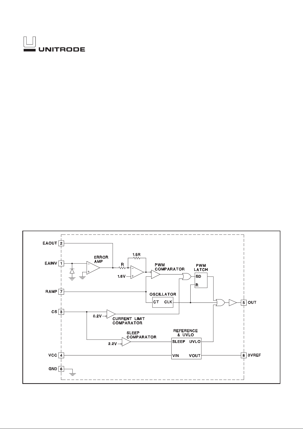
The UC3572 is a negative output flyback pulse width modulator which converts a positive input voltage to a regulated negative output voltage. The
chip is optimized for use in a single inductor negative flyback switching
converter employing an external PMOS switch. The block diagram consists
of a precision reference, an error amplifier configured for voltage mode operation, an oscillator, a PWM comparator with latching logic, and a 0.5A
peak gate driver. The UC3572 includes an undervoltage lockout circuit to
insure sufficient input supply voltage is present before any switching activity can occur, and a pulse-by-pulse current limit. Output current can be
sensed and limited to a user determined maximum value. The UVLO circuit
turns the chip off when the input voltage is below the UVLO threshold. In
addition, a sleep comparator interfaces to the UVLO circuit to turn the chip
off. This reduces the supply current to only 50µA, making the UC3572 ideal
for battery powered applications.
Negative Output Flyback Pulse Width Modulator
FEATURES
• Simple Single Inductor Flyback PWM
for Negative Voltage Generation
• Drives External PMOS Switch
• Contains UVLO Circuit
• Includes Pulse-by-Pulse Current Limit
• Low 50µA Sleep Mode Current
03/99
BLOCK DIAGRAM
UDG-94094-2
2
UC1572
UC2572
UC3572
ABSOLUTE MAXIMUM RATINGS
VCC. . . . . . . . . . . . . . . . . . . . . . . . . . . . . . . . . . . . . . . . . . . 35V
EAINV. . . . . . . . . . . . . . . . . . . . . . . . . . . . . . . . . . -0.6V to VCC
IEAOUT. . . . . . . . . . . . . . . . . . . . . . . . . . . . . . . . . . . . . . . . 25mA
RAMP. . . . . . . . . . . . . . . . . . . . . . . . . . . . . . . . . . . . -0.3V to 4V
CS. . . . . . . . . . . . . . . . . . . . . . . . . . . . . . . . . . . . . -0.3V to VCC
Iout . . . . . . . . . . . . . . . . . . . . . . . . . . . . . . . . . . . . -0.7A to 0.7A
I3VREF . . . . . . . . . . . . . . . . . . . . . . . . . . . . . . . . . . . . . . .-15mA
Storage Temperature . . . . . . . . . . . . . . . . . . . -65°C to +150°C
Junction Temperature . . . . . . . . . . . . . . . . . . . -65°C to +150°C
Lead Temperature (Soldering, 10 sec.). . . . . . . . . . . . . +300°C
Currents are positive into, negative out of the specified
terminal. Consult Packaging Section of Databook for thermal
limitations and considerations of packages.
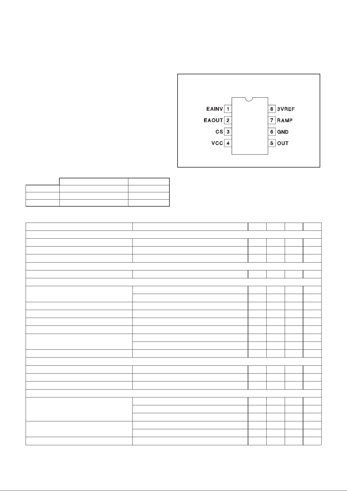
DIL-8, SOIC-8 (TOP VIEW)
D, N or J Packages
CONNECTION DIAGRAM
TEMPERATURE RANGE PACKAGE
UC1572 –55°C to +125°C J
UC2572 –40°C to +85°C D, N or J
UC3572 0°C to +70°C D or N
ORDERING INFORMATION
ELECTRICAL CHARACTERISTICS:
Unless otherwise specified, VCC = 5V, CT = 680pF, TA=T
J
.
PARAMETER TEST CONDITIONS MIN TYP MAX UNITS
Reference Section
3VREF 2.94 3 3.06 V
Line Regulation VCC = 4.75 to 30V 1 10 mV
Load Regulation I
3VREF = 0V to –5mA 1 10 mV
Oscillator Section
Frequency VCC = 5V to 30V 85 100 115 kHz
Error Amp Section
EAINV EAOUT = 2V –10 0 10 mV
I
EANV = –1mA –0.2 –0.9 V
IEAINV EAOUT = 2V –0.2 –1.0 µA
AVOL EAOUT = 0.5V to 3V 65 90 dB
EAOUT High EAINV = –100mV 3.6 4 4.4 V
EAOUT Low EAINV = 100mV 0.1 0.2 V
IEAOUT EAINV = –100mV, EAOUT = 2V –350 –500 µA
EAINV = 100mV, EAOUT = 2V 7 20 mA
Unity Gain Bandwidth TJ = 25°C, F = 10kHz 0.6 1 MHz
Current Sense Comparator Section
Threshold 0.195 0.215 0.235 V
Input Bias Current CS = 0 –0.4 –1 µA
CS Propogation Delay 300 nS
Gate Drive Output Section
OUT High Saturation I
OUT = 0 0 0.3 V
IOUT = –10mA 0.7 1.5 V
IOUT = –100mA 1.5 2.5 V
OUT Low Saturation IOUT = 10mA 0.1 0.4 V
IOUT = 100mA 1.5 2.2 V
Rise Time TJ = 25°C, CLOAD = 1nF + 3.3 Ohms 30 80 nS
3
UC1572
UC2572
UC3572
ELECTRICAL CHARACTERISTICS:
Unless otherwise specified, VCC = 5V, CT = 680pF, TA=T
J
.
PARAMETER TEST CONDITIONS MIN TYP MAX UNITS
Fall Time TJ = 25°C, CLOAD = 1nF + 3.3 Ohms 30 80 nS
Pulse Width Modulator Section
Maximum Duty Cycle EAINV = +100mV, VCC = 5V to 30V 92 96 %
Minimum Duty Cycle EAINV = –100mV, VCC = 5V to 30V 0 %
Modulator Gain EAOUT = 1.5V to 2.5V 45 55 65 %/V
Undervoltage Lockout Section
Start Threshold 3.5 4.2 4.5 V
Hysteresis 100 200 300 mV
Sleep Mode Section
Threshold 1.8 2.2 2.6 V
Supply Current Section
IVCC VCC = 5V, 30V 9 12 mA
VCC = 30, CS = 3V 50 150 µA
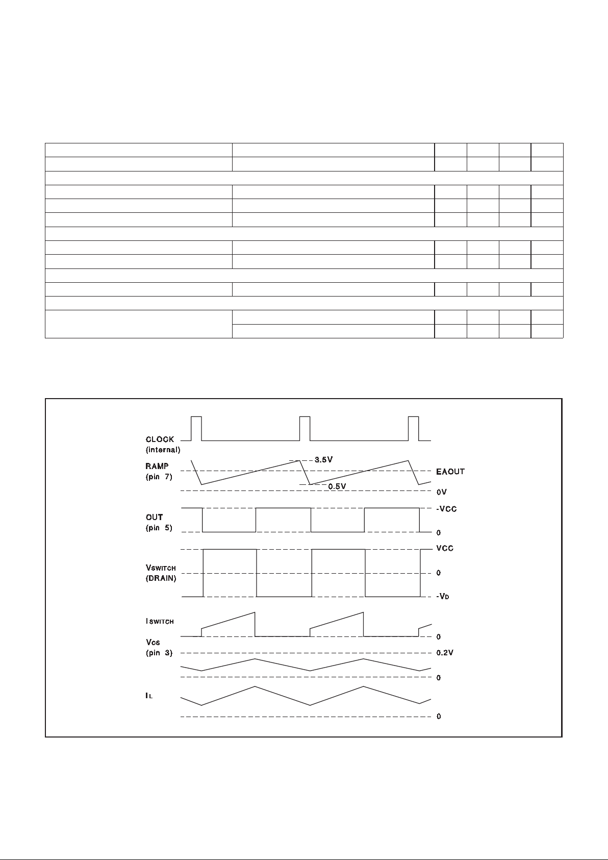
Figure 1. Typical waveforms.
UDG-94095
4
UC1572
UC2572
UC3572
4
8
7
1
2
6
5
3
R
SLEEP1
56k
R
SLEEP2
33k
R
COMP
R
REF
RV
SENSE
40k
RSLEEP3
1MEG
R
CS
C
IN
10µF
COUT
100µF
VOUT
GND
–12V OUT
D
FLYBACK
L
FLYBACK
M
SWITCH
C
RAMP
680pF
CV
CC
10µF
M
SLEEP
GND
SLEEP
VIN
VCC
3VREF
RAMP
EAINV
EAOUT
GND
CS
OUT
UC1572
C3V
REF
100nF
C
COMP
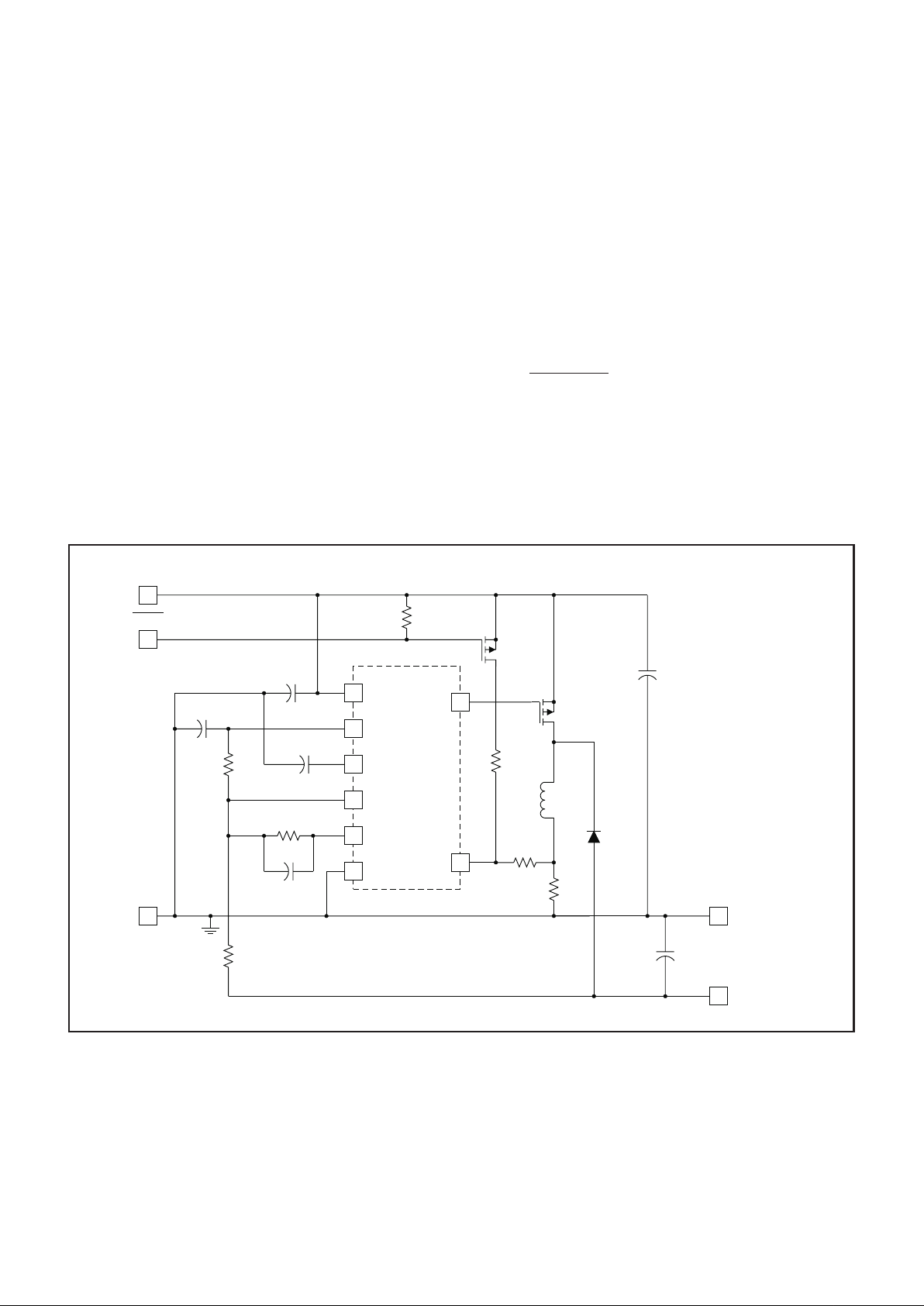
Figure 2. Typical application: +5V to –12V flyback converter.
UDG-99057
UNITRODE CORPORATION
7 CONTINENTALBLVD. • MERRIMACK, NH 03054
TEL. (603) 424-2410 • FAX (603) 424-3460
PIN DESCRIPTIONS
3VREF: Precision 3V reference. Bypass with 100nF ca-
pacitor to GND.
CS: Current limit sense pin. Connect to a ground refer-
enced current sense resistor in series with the flyback inductor. OUT will be held high (PMOS switch off) if CS
exceeds 0.2V.
EAINV: Inverting input to error amplifier. Summing junction for 3VREF and VOUT sense. The non-inverting input
of the error amplifier is internally connected to GND. This
pin will source a maximum of 1mA.
EAOUT: Output of error amplifier. Use EAOUT and
EAINV for loop compensation components.
GND: Circuit Ground.
OUT: Gate drive for external PMOS switch connected
between V
CC and the flyback inductor. OUT drives the
gate of the PMOS switch between VCC and GND.
RAMP: Oscillator and ramp for pulse width modulator.
Frequency is set by a capacitor to GND by the equation
F
kC
RAMP
=
•
1
15
Recommended operating frequency range is 10kHz to
200kHz.
VCC: Input voltage supply to chip. Range is 4.75 to 30V.
Bypass with a 1µF capacitor.

IMPORTANT NOTICE
T exas Instruments and its subsidiaries (TI) reserve the right to make changes to their products or to discontinue
any product or service without notice, and advise customers to obtain the latest version of relevant information
to verify, before placing orders, that information being relied on is current and complete. All products are sold
subject to the terms and conditions of sale supplied at the time of order acknowledgement, including those
pertaining to warranty, patent infringement, and limitation of liability.
TI warrants performance of its semiconductor products to the specifications applicable at the time of sale in
accordance with TI’s standard warranty. T esting and other quality control techniques are utilized to the extent
TI deems necessary to support this warranty. Specific testing of all parameters of each device is not necessarily
performed, except those mandated by government requirements.
CERT AIN APPLICATIONS USING SEMICONDUCTOR PRODUCTS MAY INVOLVE POTENTIAL RISKS OF
DEATH, PERSONAL INJURY, OR SEVERE PROPERTY OR ENVIRONMENTAL DAMAGE (“CRITICAL
APPLICATIONS”). TI SEMICONDUCTOR PRODUCTS ARE NOT DESIGNED, AUTHORIZED, OR
WARRANTED TO BE SUITABLE FOR USE IN LIFE-SUPPORT DEVICES OR SYSTEMS OR OTHER
CRITICAL APPLICATIONS. INCLUSION OF TI PRODUCTS IN SUCH APPLICA TIONS IS UNDERSTOOD T O
BE FULLY AT THE CUSTOMER’S RISK.
In order to minimize risks associated with the customer’s applications, adequate design and operating
safeguards must be provided by the customer to minimize inherent or procedural hazards.
TI assumes no liability for applications assistance or customer product design. TI does not warrant or represent
that any license, either express or implied, is granted under any patent right, copyright, mask work right, or other
intellectual property right of TI covering or relating to any combination, machine, or process in which such
semiconductor products or services might be or are used. TI’s publication of information regarding any third
party’s products or services does not constitute TI’s approval, warranty or endorsement thereof.
Copyright 1999, Texas Instruments Incorporated
 Loading...