

查询UC2526ADWTRG4供应商
Regulating Pulse Width Modulator
UC1526A
UC2526A
UC3526A
FEATURES
• Reduced Supply Current
• Oscillator Frequency to 600kHz
• Precision Band-Gap Reference
• 7 to 35V Operation
• Dual 200mA Source/Sink Outputs
• Minimum Output Cross-Conduction
• Double-Pulse Suppr ession Logic
• Under-Voltage Lockout
• Programmable Soft-Start
• Thermal Shutdown
• TTL/CMOS Compatible L ogic Ports
• 5 Volt Operation (V
IN = VC = V REF = 5.0V)
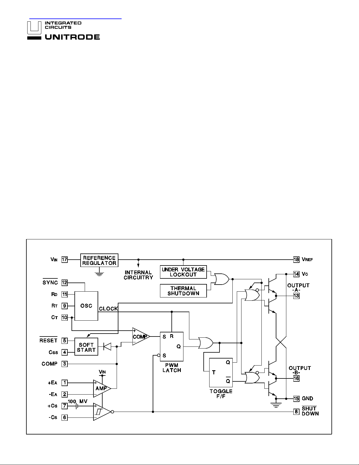
BLOCK DIAGRA M
DESCRIPTION
The UC1526A Series are improved-performance pulse-width modulator circuits intended for direct replacement of equivalent non- “A”
versions in all a pplications. Higher frequency ope ration has been
enhanced by several significant improvements including: a more accurate oscillator with less minimum dead time, reduced circuit delays (particularly i n current limiting), and an improved output stage
with negligible cross-condu ction current. Additional improvements
include the incorporation of a precisi on, band-g ap reference generator, reduced overall supply current, and the addition of thermal
shutdown protection.
Along with these improvements, the UC1526A Series retains the
protective features of under-voltage lockou t, soft-start, digital current limiting, double pulse suppression logic, and adjustable
deadtime. For ease of interfacing, all digital control ports are TTL
compatible with active low logic.
Five volt (5V) operation is possible for “logic level” applications by
connecting V
factory for additional information.
IN, VC and VREF to a precision 5V input supply. Consult
6/93
UC1526A
UC2526A
UC3526A
ABSOLUTE MAXI MUM RATING S (Note 1, 2)
Input Voltage (+VIN) . . . . . . . . . . . . . . . . . . . . . . . . . . . . . . +40V
Collector Supply Voltage (+V
C) . . . . . . . . . . . . . . . . . . . . . +40V
Logic Inputs . . . . . . . . . . . . . . . . . . . . . . . . . . . . -0.3V t o +5.5 V
Analog Input s . . . . . . . . . . . . . . . . . . . . . . . . . . . . -0.3V to +V
Source/ S ink Load Curr ent (each out pu t) . . . . . . . . . . . . 200mA
Referen ce Loa d Curr ent. . . . . . . . . . . . . . . . . . . . . . . . . . 50mA
Logic Sink Curren t . . . . . . . . . . . . . . . . . . . . . . . . . . . . . . 15mA
Power Dissipation at T
Power Dissipation at T
A = +25°C (Note 2) . . . . . . . . . 1000mW
C = +25°C (Note 2). . . . . . . . . . 3000mW
Operating Junct ion Te mp era ture . . . . . . . . . . . . . . . . . . +150°C
Storage Temperature Range . . . . . . . . . . . . . . -65°C to +150°C
Lead Tempera tu re (solder ing, 10 seconds ). . . . . . . . . . +300°C
Note 1: Values beyond which damage may oc cur.
Note 2: Consult packagin g Section of Dat aboo k for ther mal
limitations and considerations of package.
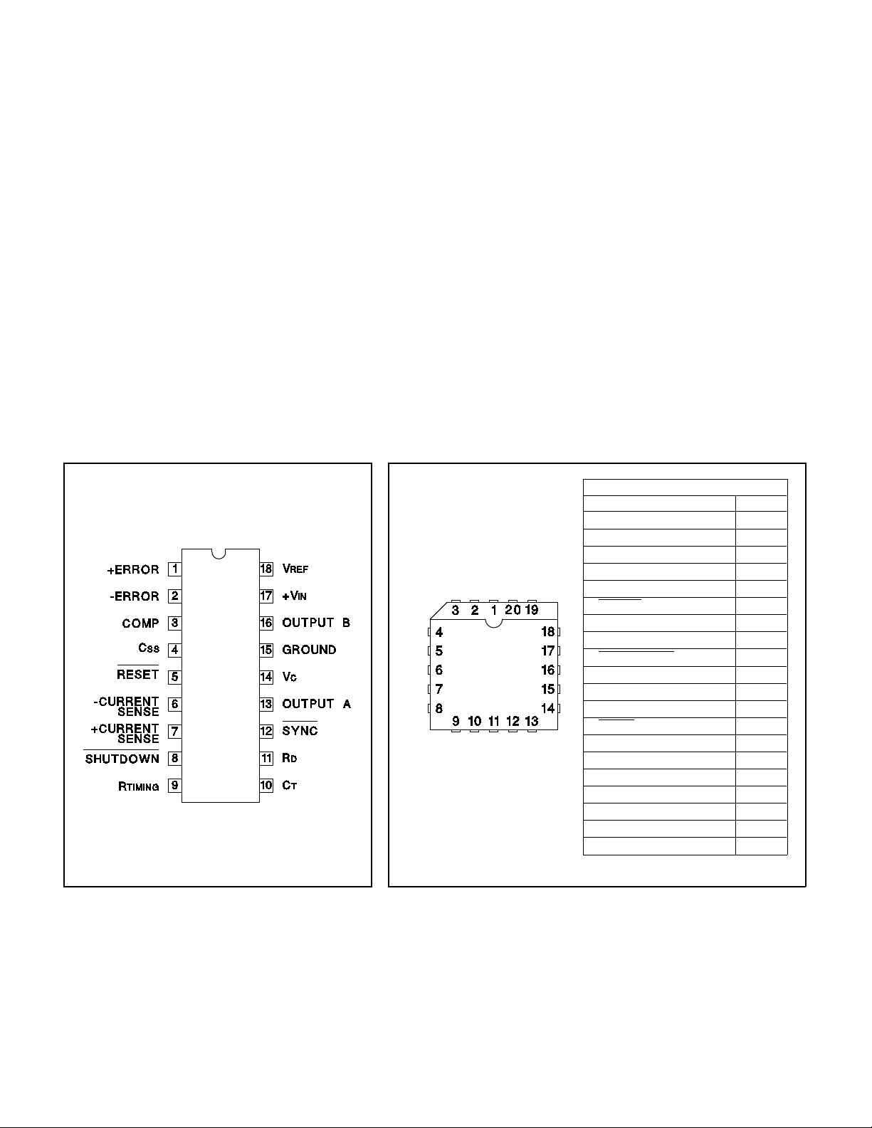
CONNECTION DIAGRAMS
DIL-18, SOIC-18 (TOP VIEW)
J or N Package, DW Package
PLCC-20, LCC- 20
(TOP VIEW)
Q and L Packages
RECOMMENDED OPERATING CONDITIONS
(Note 3)
Input Voltage. . . . . . . . . . . . . . . . . . . . . . . . . . . . . . +7V to +35V
Collector Supply Voltage . . . . . . . . . . . . . . . . . . +4.5V to +35V
Sink/Source Load Cur ren t (each output) . . . . . . . . 0 to 100m A
IN
Reference Load Cur re nt. . . . . . . . . . . . . . . . . . . . . . 0 to 20mA
Oscillator Frequency Range. . . . . . . . . . . . . . . . 1Hz to 600kHz
Oscillator Timing Resistor. . . . . . . . . . . . . . . . . . . 2k Ω to 150kΩ
Oscillator Timing Capacito r. . . . . . . . . . . . . . . . . 400pF to 20µF
Available Deadtime Range at 40kHz . . . . . . . . . . . . 1% to 50%
Operating Am bient Temperature Range
UC1526A. . . . . . . . . . . . . . . . . . . . . . . . . . . . -55°C to +125°C
UC2526A. . . . . . . . . . . . . . . . . . . . . . . . . . . . . -25°C to +85°C
UC3526A. . . . . . . . . . . . . . . . . . . . . . . . . . . . . . . 0°C to +70 ° C
Note 3: Range over which the device is functional and
parame te r limit s are guar ant eed .
PACKAGE PIN FUNCTION
FUNCTION PIN
N/C 1
+ERROR 2
-ERROR 3
COMP. 4
SS 5
C
RESET 6
- CURRENT SENSE 7
+ CURRENT SENSE 8
SHUTDOWN 9
TIMING 10
R
T 11
C
D 12
R
SYNC 13
OUTPUT A 14
C 15
V
N/C 16
GROUND 17
OUTPUT B 18
IN 19
+V
REF 20
V
2
UC1526A
UC2526A
UC3526A
+V
ELECTRICAL CHARACTERISTICS:
PARAMETER TEST CONDITIONS
Reference Sec tion (Note 4)
Output Volt age T
Line Regulatio n +V
Load Regulation I
Temperature Stability Over Operating T
Total Output Voltage
Range
Short Circuit Current V
Under-Voltage Lockout
RESET Output Voltage VREF = 3.8V 0.2 0.4 0.2 0.4 V
Oscillato r Sect io n (Note 6)
Initial Accuracy T
Voltage Stability +V
Temperature Stability Over Operating T
Minimum Frequency R
Maximum Frequency R
Sawtooth Peak Voltage + V
Sawtooth Valley Voltage +V
SYNC Pulse Width TJ = 25°C, RL = 2.7kΩ to V
Error Ampl i fier Section (Note 7)
Input Offs et Vo lta ge R
Input Bias Cur rent -350 -1000 -350 -2000 nA
Input Offs et Cu rr ent 35 100 35 200 nA
DC Open Loop Gai n R
HIGH Output Voltage V
LOW Output Voltage V
Common Mode Rejec tion R
Supply Voltage Rejection +V
PWM Comparator (Note 6)
Minimum Duty Cycle V
Maximum Duty Cycle V
Digi tal Ports (
SYNC, SHUTDOWN, and RESET)
HIGH Output Voltage I
LOW Output Voltage I
HIGH Input Current V
LOW Input Current V
Shutdown Delay From Pin 8, T
Current Limit Compar ato r (Note 8)
Sense Voltage R
Input Bias Cur rent -3 -10 -3 -10 µA
Shutdown Delay From pin 7, 100m V Over driv e, T
Note 4: I
L =
0mA.
Note 5: Guaranteed by design, not 100% tested in product ion.
Note 6: F
OSC
= 40kHz, (RT = 4.12 kΩ ± 1%, CT = 0.01µF± 1%,
D
= 0 Ω).
R
J = +25°C 4.95 5.00 5.05 4.90 5.00 5.10 V
IN = 7 to 35V 2 10 2 15 mV
L = 0 to 20mA 5 20 5 20 mV
Over Recomme nded Opera ting
Conditio ns
REF = 0V 25 50 100 25 50 100 mA
VREF = 4.7V 2.4 4.7 2.4 4.8 V
J = +25°C ±3 ±8 ±3 ±8%
IN = 7 to 35V 0.5 1 0.5 1 %
T = 150kΩ, CT = 20µF (Note 5) 1 1 Hz
T = 2kΩ, CT = 470pF 5 50 650 kHz
IN = 35V 3.0 3.5 3.0 3.5 V
IN =7V 0.5 1.0 0.5 1.0 V
S ≤ 2kΩ 25 210mV
L ≥ 10MΩ 64 72 60 72 dB
PIN 1 - VPIN 2 ≥ 150mV, ISOURCE = 100µA 3.6 4.2 3.6 4.2 V
PIN 2 - VPIN 1 ≥ 150 mV, ISINK = 100µA 0.2 0.4 0.2 0.4 V
S ≤ 2kΩ 70 94 70 94 dB
IN = 12 to 18V 66 80 66 80 dB
COMPENSATION = +0.4V 0 0 %
COMPENSATION = +3.6V 45 49 45 49 %
SOURCE = 40µA 2.4 4.0 2.4 4.0 V
SINK = 3.6mA 0.2 0.4 0 .2 0.4 V
IH = +2.4V -125 -200 -125 -200 µA
IL = +0.4V -225 -36 0 -225 -360 µA
S ≤ 50Ω 90 100 110 80 100 120 mV
IN = 15V, and over operating ambient temper ature, unless ot herwise specified TA = TJ.
UC1526A / UC2526A UC3526A
MIN TYP MAX MIN TYP MAX
J (Note 5) 15 50 15 50 mV
4.90 5.00 5.10 4.85 5.00 5.15 V
J (Note 5) 26 13%
REF
J = 25°C 160 160 ns
J = 25°C 260 260 ns
Note 7: V
Note 8: V
Note 9: V
Note 10 :V
CM
CM
C
IN
1.1 1.1 µs
= 0 to +5.2V
= 0 to +12V.
= +15V .
= +35V , RT = 4.12kΩ.
UNITS
3
UC1526A
UC2526A
UC3526A
ELECTRICAL CHARACTERISTICS:
PARAMETER TEST CONDITIONS
+VIN = 15V, and over operating ambient temperature, unless otherwise specified T A = TJ.
UC1526A
UC3526A
UC2526A
MIN TYP MAX MIN TYP MAX
Soft-Start Sec tion
Error Clamp Voltage
C
S Charging Current RESET = +2.4V 50 100 150 50 100 150 µA
RESET = +0.4V 0.1 0.4 0.1 0 .4 V
Output Drivers (Each Output) (Note 9)
HIGH Output Voltage I
LOW Output Voltage I
Collector Leakage V
Rise Time C
Fall Time C
Cross-Conductio n Charge Per cycle, T
SOURCE = 20mA 12.5 13.5 12.5 13.5 V
SOURCE = 100m A 12 13 12 13 V
I
SINK = 20mA 0.2 0.3 0.2 0.3 V
I
SINK = 100mA 1.2 2.0 1.2 2.0 V
C = 40V 50 150 50 150 µA
L = 1000pF (Note 5) 0.3 0.6 0.3 0.6 µs
L = 1000pF (Note 5) 0.1 0.2 0.1 0.2 µs
J = 25°C 8 8 nC
Power Consumption (Note 10)
Standby Current
Note 4: I
L =
0mA.
SHUTDOWN = +0.4V 14 20 14 20 mA
Note 5: Guaranteed by design, not 100% tested in product ion.
Note 6: F
Note 7: V
Note 8: V
Note 9: V
Note 10 :V
OSC
= 40kHz, (RT = 4.12 kΩ ± 1%, CT = 0.01µF± 1%,
D
= 0 Ω).
R
CM
= 0 to +5.2V
CM
= 0 to +12V.
C
= +15V .
IN
= +35V , RT = 4.12kΩ.
UNITS
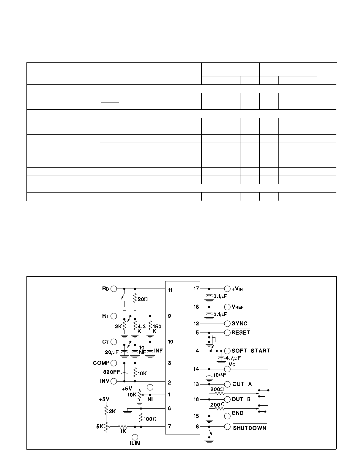
Open Loop Test Circ uit UC15 26A
4
APPLICATIONS INFORMATION
Volt age Reference
The reference regulator of the UC1526A is based on a
precision band-gap reference, internally trimmed to ±1%
accuracy. The circui try is fully active at supply voltages
above +7V, and provides up to 20mA of load current to
external circuitry a t +5.0V. In systems where additional
current is required, an externa l PNP transistor can be
used to boost the available current. A rugged low frequency audio-type transistor should be used, and lead
lengths between the PWM and transistor should be as
short as possible to minimize the risk of oscillations.
Even so, some types of transistors may require collector-base capacitance for stability. Up to 1 amp of load
current can be obtai ned with excelle nt regulation if the
device selected maintains high current ga in.
Figure 1. Extending Reference O ut put Curr ent
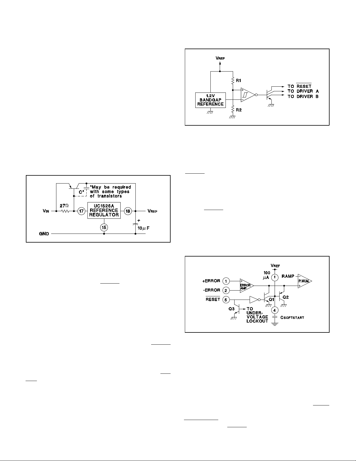
Under-V olta ge Loc kout
The under-voltage locko ut circuit protects the UC1526A
and the power devices it controls from inadequate supply voltage , If +V
output drivers and holds the
vents spurious output pulses while the control circuitry is
stabilizing, and holds the soft-start timing capaci tor in a
discharged state.
IN is too low, the circuit disables the
RESET pin LOW. This pre-
UC1526A
UC2526A
UC3526A
Figure 2. Under-Voltage Loc kout Schemat ic
Soft-Start Circuit
The soft-start circuit protects the power transistors and
rectifier diodes from high curren t surges during power
supply turn-on. When supply voltage is first applied to
the UC1526A, the under-voltage lockout circuit holds
RESET LOW with Q3. Q1 is turned on, which holds the
soft-start capacitor voltage at zero. The second collector
of Q
1 clamps the outpu t of the error amplifier to ground,
guaranteeing zero duty cycle at the driver outputs.
When the supply voltage reaches normal operating
range,
internal 100µA current source to charge C
the error amplifier output to 1V
C
cycle of the PWM l inearly increases to whatever value
the voltage regulation loop requires for an error null.
RESET will go HIGH. Q1 turns off, allowing the
S. Q2 clamps
BE above the voltage on
S. As the soft-start voltage ramps up to +5V, the duty
The circuit consi sts of a +1.2V bandgap reference and
comparator circuit which is active when the reference
voltage has risen t o 3V
BE or +1.8V at 25°C. When the
reference voltage rises to approximately +4.4V, the circuit enables the output drivers and rele ases the
RESET
pin, allowing a normal soft-start. The comparator has
350mV of hysteresis to minimize oscillation at the trip
point. When +V
ence drops to +4.2V, the under-voltage circuit pulls
IN to the PWM is removed and the refer-
RESET LOW again. The soft-start capacitor is immediately
discharged, and the PWM is re ady for another soft-start
cycle.
The UC1526A can operate from a +5V supply by connecting the V
REF pin to the +VIN pin and maintaining the
supply between +4.8 and +5.2V.
Figure 3. Soft-Start Circuit Schematic
Digital Control Ports
The three digital control ports of the UC1526A are bi-directional. Each pin can drive TTL and 5V CMOS logic directly, up to a fan-out of 10 low-power Schottky gates.
Each pin can also be directly driven by open-collector
TTL, open-drain CMOS, and open-collector voltage
comparators; fan-in is equivalent to 1 low-power Schottky gate. Each port i s normally HIGH; the pi n is pulled
LOW to activate the particular function. Driving
LOW initiates a discha rge cycle in the osci llator. Pulling
SHUTDOWN LOW immediately inhibits all PWM output
pulses. Holding
RESET LOW discharges the soft-start
5
SYNC

APPLICATIONS INFORMATION (cont.)
capacitor. The logic threshol d is +1.1V at +25°C. Noise
immunity can be gained at the expense of fan-out with an
external 2k pull-up resistor to +5V.
UC1526A
UC2526A
UC3526A
the SYNC pin will then lock the oscillator to the external
frequency.
Multiple devices can be synchronized together by programming one master unit for the desired frequency, and
then sharing its sawtooth and clock waveforms with the
slave units. All C
of the master and all
nected to the
nals are left open or connected to V
terminal may be either left open or grounded.
T terminals are connected to the CT pin
SYNC terminals are likewise con-
SYNC pin of the master. Slave RT termi-
REF. Slave RD
Figure 4.
Digital Co ntr ol Port Schematic
Oscillators
The oscillator is programmed for frequency and dead
time with three components: R
forms are generated : a sawtooth waveform at pin 10 for
pulse width modulation, and a logic clock at pin 12. The
following procedure is recommended for choosing timing
values:
1. With R
RT and CT from the graph on page 4 to give the de-
for
D= 0Ω (pi n 11 shorted to ground) select values
sired oscilla tor period. Remember that the frequency at
each driver output is half the oscillator frequency, and the
frequency at the +V
C terminal is the same as the oscilla-
tor frequency.
2. If more dead time is required, select a larger value of
D. At 40kHz dead time increases by 400ns/ Ω.
R
3. Increasing the dead time will cause the oscillator frequency to decrease slig htly. Go back and decrease the
value of R
T slightly to bring the frequency back to the
nominal design value.
The UC1526A can be synchronized to an external logic
clock by programming the oscillator to free-run at a frequency 10% slower than the
T, CT and RD. Two wave-
SYNC frequency.
Figure 6. Error Amplifier C onnections
Error Amplifie r
The error amplifier is a transconductance design, with an
output impedance of 2MΩ. Since all vo ltage gain takes
place at the output pin, the open-loop gain/frequency
characteristics can be controlled with shunt reactance to
ground. When compensated for unity-gain stability with
100pF, the amplifier has an open-loop pole at 800Hz.
The input connections to the error amplifier are determined by the pola rity of the swi tchin g supp ly output voltage. For positive supplies, the common-mode voltage is
+5.0V and the feedback connections in Figure 6A are
used. With negative supplies, the common-mode voltage
is ground and the feedback divider is connected between
the negative output an d the +5.0V reference voltage, as
shown in Figure 6B.
A period ic LOW logic pulse appro ximately 0.5µs wide at
Figure 5. Oscillator Connections and Waveforms
Figure 7. Push-Pull Configuration
6
OUTPUT BLANKING
APPLICATIONS INFORMATION (cont.)
Output Drivers
The totem pole output drivers of the UC1526A are designed to source and sink 100mA continuously and
200mA peak. Loads can be driven either from the output
pins 13 and 16, or from the +V
Since the bottom transistor of the totem-pole is allowed to
saturate, there is a momentary condu ction path from the
C, as required.
UC1526A
UC2526A
UC3526A
+V
C terminal to ground during switching; however, im-
proved design has limited this cross-conduction period to
less than 50ns. Capacitor decoupling at V
mended and careful g rounding of Pin 15 is needed to insure that high peak sink currents from a capacitive load
do not cause ground transients.
C is recom-
Figure 8. Single-Ended Conf i gur ation
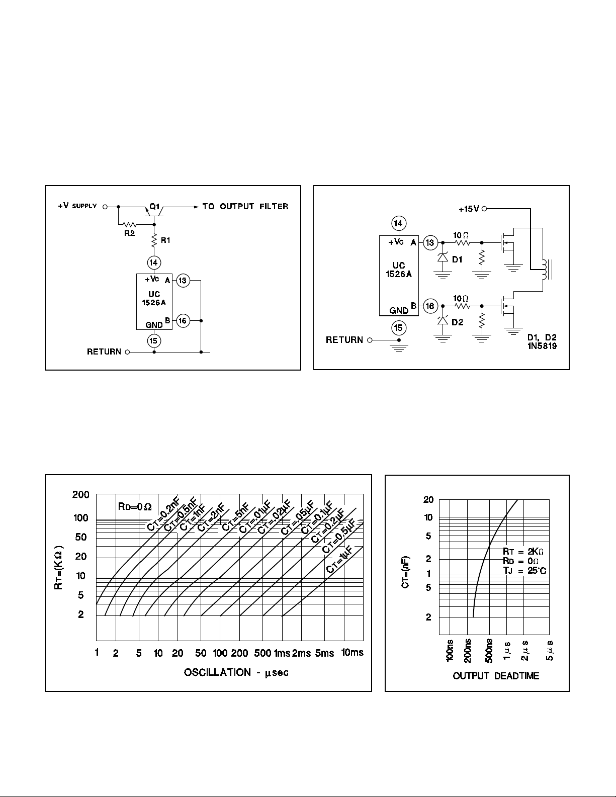
TYPICAL CHARACTERIS TICS
OSCILLATOR PERIOD vs RT and CT
Figure 9. Driving N-Channel Power MOSFETs
7
TYPICAL CHARACTERIS TICS (Co nt.)
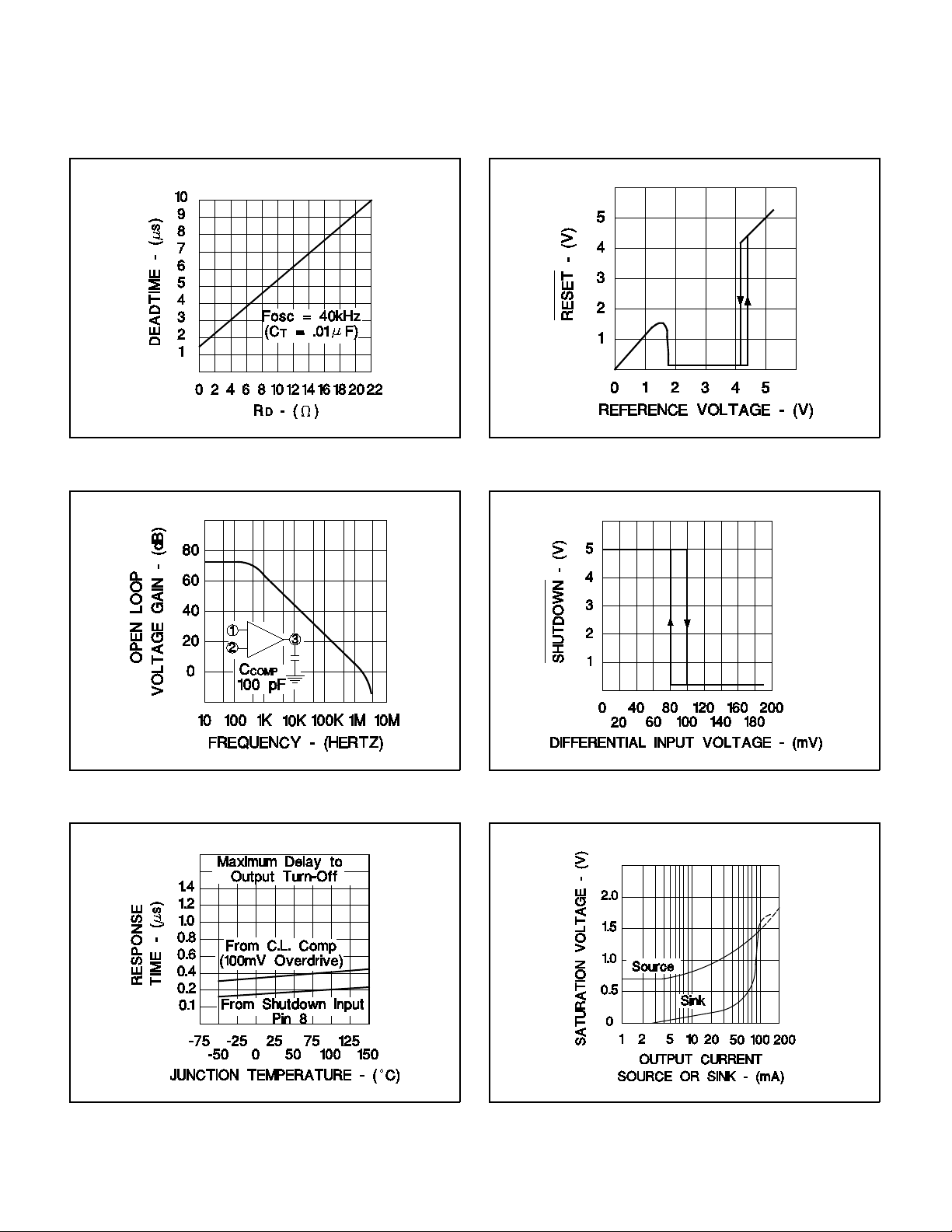
Output Driver Deadtime vs. RD Value Under Voltage Lockout Characteristic
UC1526A
UC2526A
UC3526A
Error Amplifier Open Loop Gain vs. Freq u ency
Shutdow n Delay Output Driver Saturation Voltage
Current Limit Transfer Function
UNITRODE INTEGRATED CIRCUITS
7 CONTINENTAL BLVD. • MERRIMACK, NH 03054
TEL. (603) 424-2410 • FAX (603) 424-3460
8

PACKAGE OPTION ADDENDUM
www.ti.com
15-Nov-2005
PACKAGING INFORMATION
Orderable Device Status
(1)
Package
Type
Package
Drawing
Pins Package
Qty
Eco Plan
85515022A ACTIVE LCCC FK 20 1 TBD POST-PLATE Level-NC-NC-NC
8551502VA ACTIVE CDIP J 18 1 TBD A42 SNPB Level-NC-NC-NC
UC1526AJ ACTIVE CDIP J 18 1 TBD A42 SNPB Level-NC-NC-NC
UC1526AJ883B ACTIVE CDIP J 18 1 TBD A42 SNPB Level-NC-NC-NC
UC1526AL ACTIVE LCCC FK 20 1 TBD POST-PLATE Level-NC-NC-NC
UC1526AL883B ACTIVE LCCC FK 20 1 TBD POST-PLATE Level-NC-NC-NC
UC2526ADW ACTIVE SOIC DW 18 40 Green (RoHS &
no Sb/Br)
UC2526ADWTR ACTIVE SOIC DW 18 2000 Green (RoHS &
no Sb/Br)
UC2526ADWTRG4 ACTIVE SOIC DW 18 2000 Green (RoHS &
no Sb/Br)
UC2526AJ ACTIVE CDIP J 18 1 TBD A42 SNPB Level-NC-NC-NC
UC2526AN ACTIVE PDIP N 18 20 Green (RoHS &
no Sb/Br)
UC2526ANG4 ACTIVE PDIP N 18 20 Green (RoHS &
no Sb/Br)
UC2526AQ ACTIVE PLCC FN 20 46 Green (RoHS &
no Sb/Br)
UC3526ADW ACTIVE SOIC DW 18 40 Green (RoHS &
no Sb/Br)
UC3526ADWG4 ACTIVE SOIC DW 18 40 Green (RoHS &
no Sb/Br)
UC3526ADWTR ACTIVE SOIC DW 18 2000 Green (RoHS &
no Sb/Br)
UC3526ADWTRG4 ACTIVE SOIC DW 18 2000 Green (RoHS &
no Sb/Br)
UC3526AJ ACTIVE CDIP J 18 1 TBD A42 SNPB Level-NC-NC-NC
UC3526AN ACTIVE PDIP N 18 20 Green (RoHS &
no Sb/Br)
UC3526ANG4 ACTIVE PDIP N 18 20 Green (RoHS &
no Sb/Br)
UC3526AQ ACTIVE PLCC FN 20 46 Green (RoHS &
no Sb/Br)
(1)
The marketing status values are defined as follows:
ACTIVE: Product device recommended for new designs.
LIFEBUY: TI has announced that the device will be discontinued, and a lifetime-buy period is in effect.
NRND: Not recommended for new designs. Device is in production to support existing customers, but TI does not recommend using this part in
a new design.
PREVIEW: Device has been announced but is not in production. Samples may or may not be available.
OBSOLETE: TI has discontinued the production of the device.
(2)
Lead/Ball Finish MSL Peak Temp
CU NIPDAU Level-2-260C-1 YEAR
CU NIPDAU Level-2-260C-1 YEAR
CU NIPDAU Level-2-260C-1 YEAR
CU NIPDAU Level-NC-NC-NC
CU NIPDAU Level-NC-NC-NC
CU SN Level-2-260C-1 YEAR
CU NIPDAU Level-2-260C-1 YEAR
CU NIPDAU Level-2-260C-1 YEAR
CU NIPDAU Level-2-260C-1 YEAR
CU NIPDAU Level-2-260C-1 YEAR
CU NIPDAU Level-NC-NC-NC
CU NIPDAU Level-NC-NC-NC
CU SN Level-2-260C-1 YEAR
(3)
(2)
Eco Plan - The planned eco-friendly classification: Pb-Free (RoHS) or Green (RoHS & no Sb/Br) - please check
http://www.ti.com/productcontent for the latest availability information and additional product content details.
TBD: The Pb-Free/Green conversion plan has not been defined.
Pb-Free (RoHS): TI's terms "Lead-Free" or "Pb-Free" mean semiconductor products that are compatible with the current RoHS requirements
for all 6 substances, including the requirement that lead not exceed 0.1% by weight in homogeneous materials. Where designed to be soldered
at high temperatures, TI Pb-Free products are suitable for use in specified lead-free processes.
Green (RoHS & no Sb/Br): TI defines "Green" to mean Pb-Free (RoHS compatible), and free of Bromine (Br) and Antimony (Sb) based flame
retardants (Br or Sb do not exceed 0.1% by weight in homogeneous material)
Addendum-Page 1

PACKAGE OPTION ADDENDUM
www.ti.com
(3)
MSL, Peak Temp. -- The Moisture Sensitivity Level rating according to the JEDEC industry standard classifications, and peak solder
temperature.
Important Information and Disclaimer:The information provided on this page represents TI's knowledge and belief as of the date that it is
provided. TI bases its knowledge and belief on information provided by third parties, and makes no representation or warranty as to the
accuracy of such information. Efforts are underway to better integrate information from third parties. TI has taken and continues to take
reasonable steps to provide representative and accurate information but may not have conducted destructive testing or chemical analysis on
incoming materials and chemicals. TI and TI suppliers consider certain information to be proprietary, and thus CAS numbers and other limited
information may not be available for release.
In no event shall TI's liability arising out of such information exceed the total purchase price of the TI part(s) at issue in this document sold by TI
to Customer on an annual basis.
15-Nov-2005
Addendum-Page 2

IMPORTANT NOTICE
Texas Instruments Incorporated and its subsidiaries (TI) reserve the right to make corrections, modifications,
enhancements, improvements, and other changes to its products and services at any time and to discontinue
any product or service without notice. Customers should obtain the latest relevant information before placing
orders and should verify that such information is current and complete. All products are sold subject to TI’s terms
and conditions of sale supplied at the time of order acknowledgment.
TI warrants performance of its hardware products to the specifications applicable at the time of sale in
accordance with TI’s standard warranty. Testing and other quality control techniques are used to the extent TI
deems necessary to support this warranty . Except where mandated by government requirements, testing of all
parameters of each product is not necessarily performed.
TI assumes no liability for applications assistance or customer product design. Customers are responsible for
their products and applications using TI components. To minimize the risks associated with customer products
and applications, customers should provide adequate design and operating safeguards.
TI does not warrant or represent that any license, either express or implied, is granted under any TI patent right,
copyright, mask work right, or other TI intellectual property right relating to any combination, machine, or process
in which TI products or services are used. Information published by TI regarding third-party products or services
does not constitute a license from TI to use such products or services or a warranty or endorsement thereof.
Use of such information may require a license from a third party under the patents or other intellectual property
of the third party, or a license from TI under the patents or other intellectual property of TI.
Reproduction of information in TI data books or data sheets is permissible only if reproduction is without
alteration and is accompanied by all associated warranties, conditions, limitations, and notices. Reproduction
of this information with alteration is an unfair and deceptive business practice. TI is not responsible or liable for
such altered documentation.
Resale of TI products or services with statements different from or beyond the parameters stated by TI for that
product or service voids all express and any implied warranties for the associated TI product or service and
is an unfair and deceptive business practice. TI is not responsible or liable for any such statements.
Following are URLs where you can obtain information on other Texas Instruments products and application
solutions:
Products Applications
Amplifiers amplifier.ti.com Audio www.ti.com/audio
Data Converters dataconverter.ti.com Automotive www.ti.com/automotive
DSP dsp.ti.com Broadband www.ti.com/broadband
Interface interface.ti.com Digital Control www.ti.com/digitalcontrol
Logic logic.ti.com Military www.ti.com/military
Power Mgmt power.ti.com Optical Networking www.ti.com/opticalnetwork
Microcontrollers microcontroller.ti.com Security www.ti.com/security
Telephony www.ti.com/telephony
Video & Imaging www.ti.com/video
Wireless www.ti.com/wireless
Mailing Address: Texas Instruments
Post Office Box 655303 Dallas, Texas 75265
Copyright 2005, Texas Instruments Incorporated

Copyright © Each Manufacturing Company.
All Datasheets cannot be modified without permission.
This datasheet has been download from :
www.AllDataSheet.com
100% Free DataSheet Search Site.
Free Download.
No Register.
Fast Search System.
www.AllDataSheet.com
 Loading...