Advanced Regulating Pulse Width Modulators
UC1524
UC2524
UC3524
FEATURES
Complete PWM Power Control
•
Circuitry
Uncommitted Outputs for
•
Single-ended or Push-pull
Applications
Low Standby Current…8mA Typical
•
Interchangeable with SG1524,
•
SG2524 and SG3524, Respectively
DESCRIPTION
The UC1524, UC2524 and UC3524 incorporate on a single monolithic chip
all the functions required for the construction of regulating power supplies, in
verters or switching regulators. They can also be used as the control element
for high-power-output applications. The UC1524 family was designed for
switching regulators of either polarity, transformer-coupled dc-to-dc convert
ers, transformerless voltage doublers and polarity converter applications em
ploying fixed-frequency, pulse-width modulation techniques. The dual
alternating outputs allow either single-ended or push-pull applications. Each
device includes an on-chip reference, error amplifier, programmable oscilla
tor, pulse-steering flip-flop, two uncommitted output transistors, a high-gain
comparator, and current-limiting and shut-down circuitry. The UC1524 is
characterized for operation over the full military temperature range of -55°C
to +125°C. The UC2524 and UC3524 are designed for operation from -25°C
to +85°C and 0° to +70°C, respectively.
-
-
-
-
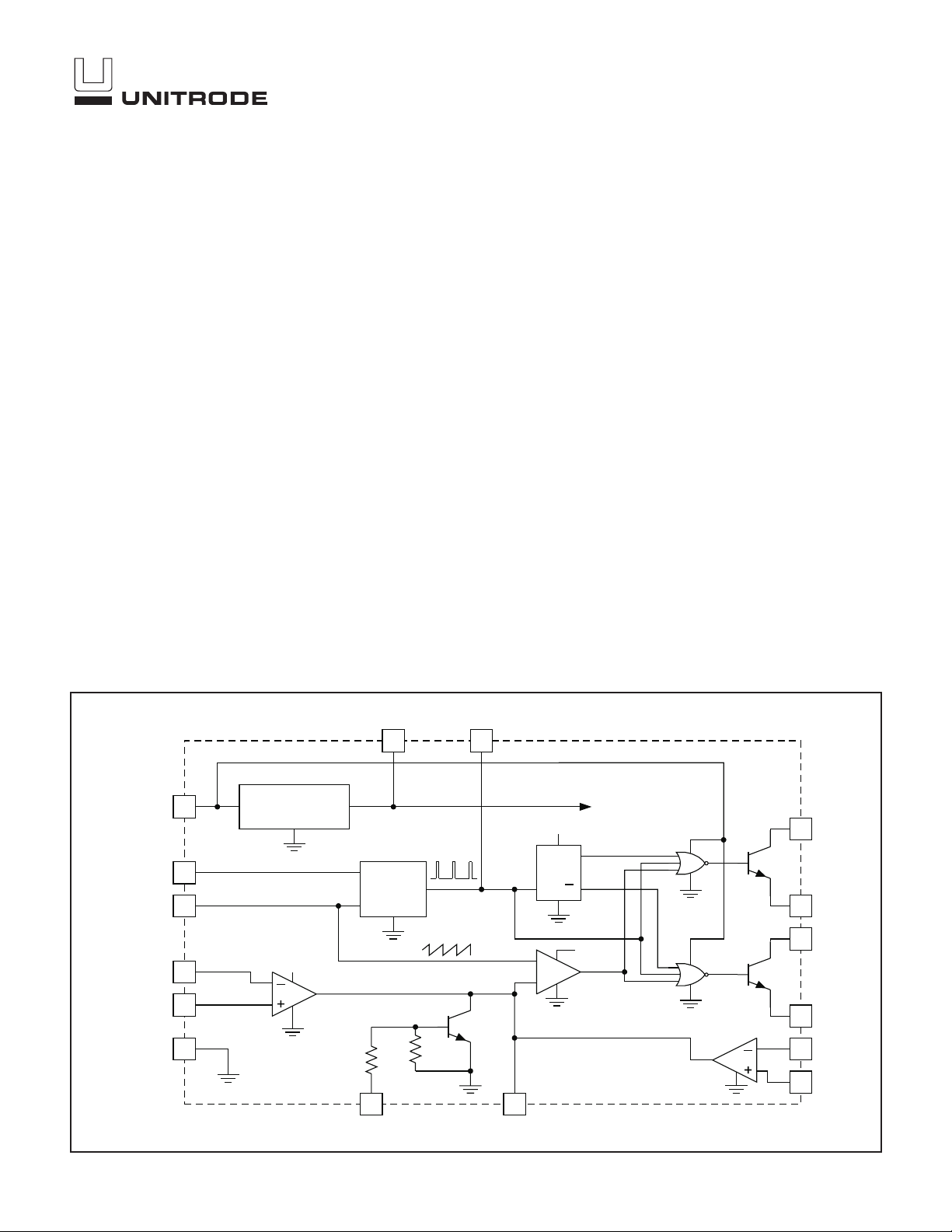
BLOCK DIAGRAM
15
V
IN
6
R
T
7
C
T
(RAMP)
INV INPUT
NI INPUT
GROUND
(SUBSTRATE)
1
2
8
REFERENCE
REGULATOR
+5V
EA
10
V
REF
16
OSC
1k
OSC OUT
COMPARATOR
10k
3
+5V TO ALL
INTERNAL
Q
QR
CIRCUITRY
+5V
CL
11
13
14
5
4
C
A
E
A
C
B
E
B
–SENSE
+SENSE
+5V 12
9
SLUS180A - NOVEMBER 1999
SHUTDOWN
COMPENSATION

ABSOLUTE MAXIMUM RATINGS (Note 1)
Supply Voltage, VCC(Notes 2 and 3) . . . . . . . . . . . . . . . . . 40V
Collector Output Current. . . . . . . . . . . . . . . . . . . . . . . . . 100mA
Reference Output Current . . . . . . . . . . . . . . . . . . . . . . . . 50mA
Current Through C
Power Dissipation at T
Power Dissipation at T
Terminal . . . . . . . . . . . . . . . . . . . . . . –5mA
T
= +25°C (Note 4). . . . . . . . . . 1000mW
A
= +25°C (Note 4). . . . . . . . . . 2000mW
C
Operating Junction Temperature Range . . . . –55°C to +150°C
Storage Temperature Range . . . . . . . . . . . . . –65°C to +150°C
Note 1: Over operating free-air temperature range unless oth
erwise noted.
Note 2: All voltage values are with respect to the ground termi
nal, pin 8.
Note 3: The reference regulator may be bypassed for opera
tion from a fixed 5V supply by connecting the V
CC
-
and
reference output pins both to the supply voltage. In this
configuration the maximum supply voltage is 6V.
Note 4: Consult packaging section of databook for thermal lim
itations and considerations of package.
RECOMMENDED OPERATING CONDITIONS
Supply Voltage, VCC. . . . . . . . . . . . . . . . . . . . . . . . . . 8V to 40V
Reference Output Current . . . . . . . . . . . . . . . . . . . . . 0 to 20mA
Current through C
Timing Resistor, R
Timing Capacitor, C
Operating Ambient Temperature Range
UC1524 . . . . . . . . . . . . . . . . . . . . . . . . . . . . –55°C to +125°C
UC2524 . . . . . . . . . . . . . . . . . . . . . . . . . . . . . –25°C to +85°C
UC3524 . . . . . . . . . . . . . . . . . . . . . . . . . . . . . . . 0°C to +70°C
Terminal . . . . . . . . . . . . . –0.03mA to –2mA
T
. . . . . . . . . . . . . . . . . . . . . 1.8kΩ to 100kΩ
T
. . . . . . . . . . . . . . . . . . . 0.001µF to 0.1µF
T
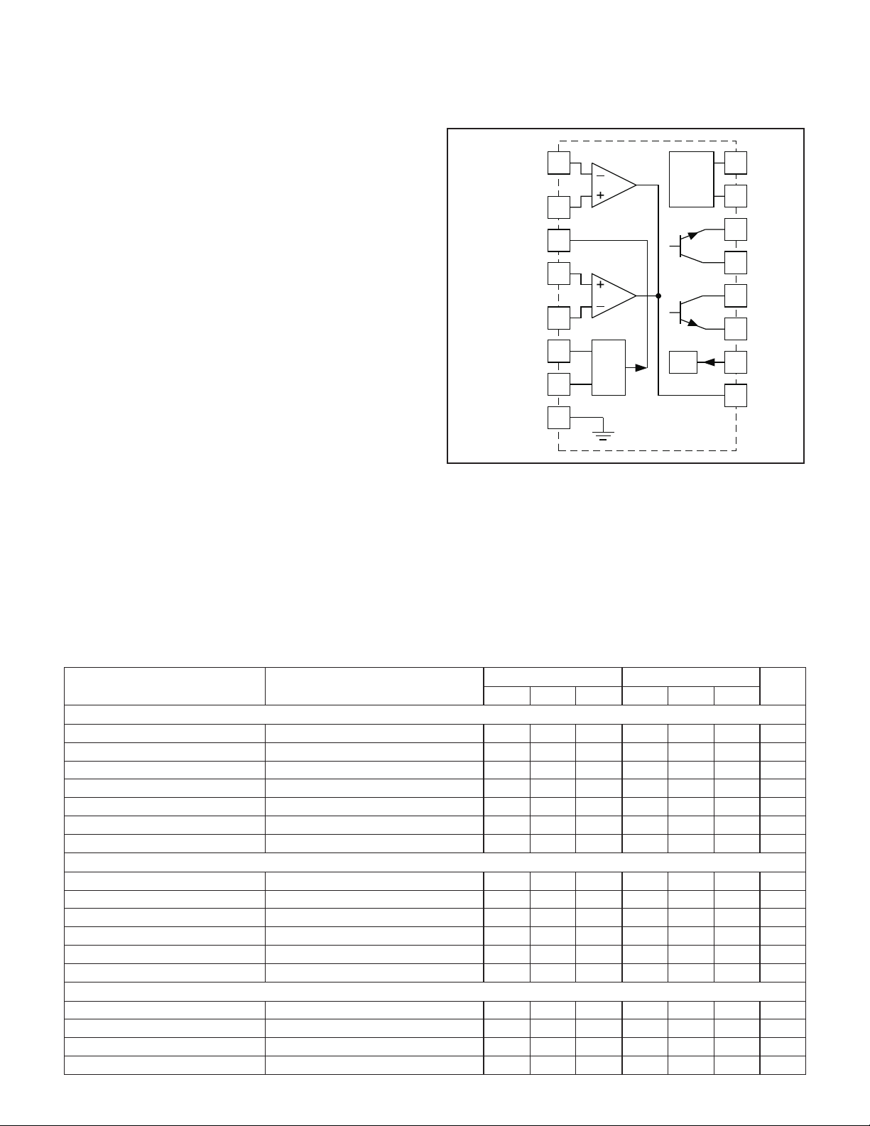
CONNECTION DIAGRAM
INV INPUT
NON INV
INPUT
OSC OUT
-
-
-
CLSENSE(+)
CLSENSE (–-)
R
C
GND
T
T
UC1524
UC2524
UC3524
1
EA
2
3
4
CL
5
6
OSC
7
8
REF
REG
S/D
16
15
14
13
12
11
10
V
REF
V
IN
E
B
C
B
C
A
E
A
S/D
9
COMP
ELECTRICAL CHARACTERISTICS: Unless otherwise stated, these specifications apply for T
for the UC1524, –25°C to +85°C for the UC2524, and 0°C to +70°C for the UC3524, V
T
A=TJ
.
= 20V, and f = 20kHz,
IN
= –55°C to +125°C
A
UC1524/UC2524 UC3524 UNITS
PARAMETER TEST CONDITIONS
MIN MAX MIN MAX
Reference Section
Output Voltage 4.8 5.0 5.2 4.6 5.0 5.4 V
Line Regulation V
Load Regulation I
Ripple Rejection f = 120Hz, T
Short Circuit Current Limit V
IN = 8 to 40V 10 20 10 30 mV
L = 0 to 20mA 20 50 20 50 mV
J = 25°C 66 66 dB
REF = 0, TJ = 25°C 100 100 mA
Temperature Stability Over Operating Temperature Range 0.3 1 0.3 1 %
Long Term Stability T
J = 125°C, t = 1000 Hrs. 20 20 mV
Oscillator Section
Maximum Frequency C
Initial Accuracy R
Voltage Stability V
= .001mfd, RT= 2kΩ 300 300 kHz
T
and CTConstant 5 5 %
T
= 8 to 40V, TJ= 25°C 1 1 %
IN
Temperature Stability Over Operating Temperature Range 5 5 %
Output Amplitude Pin 3, T
Output Pulse Width C
T
= 25°C 3.5 3.5 V
J
= .01mfd, TJ= 25°C 0.5 0.5
Error Amplifier Section
Input Offset Voltage V
Input Bias Current V
= 2.5V 0.5 5 2 10 mV
CM
= 2.5V 2 10 2 10
CM
Open Loop Voltage Gain 72 80 60 80 dB
Common Mode Voltage T
= 25°C 1.8 3.4 1.8 3.4 V
J
2
µs
µA
 Loading...