

Texas Instruments TXB0104D, TXB0104PWR, TXB0104RUTR, TXB0104YZTR, TXB0104ZXUR Schematic [ru]
Product
Folder
Sample &
Buy
Technical
Documents
Tools &
Software
Support &
Community
TXB0104
SCES650G –APRIL 2006–REVISED NOVEMBER 2014
TXB0104 4-Bit Bidirectional Voltage-level Translator With Automatic Direction Sensing
and ±15-kV ESD Protection
1 Features 3 Description
1
• 1.2 V to 3.6 V on A Port and 1.65 V to 5.5 V on B
Port (V
CCA
≤ V
CCB
)
• VCCIsolation Feature – If Either VCCInput Is at
GND, All Outputs Are in the High-Impedance
State
• OE Input Circuit Referenced to V
• Low Power Consumption, 5-μA Max I
• I
Supports Partial-Power-Down Mode Operation
off
CCA
CC
• Latch-Up Performance Exceeds 100 mA Per
JESD 78, Class II
• ESD Protection Exceeds JESD 22
– A Port
– 2500-V Human-Body Model (A114-B)
– 1500-V Charged-Device Model (C101)
– B Port
– ±15-kV Human-Body Model (A114-B)
– 1500-V Charged-Device Model (C101)
2 Applications
• Headset
• Smartphone
• Tablet
• Desktop PC
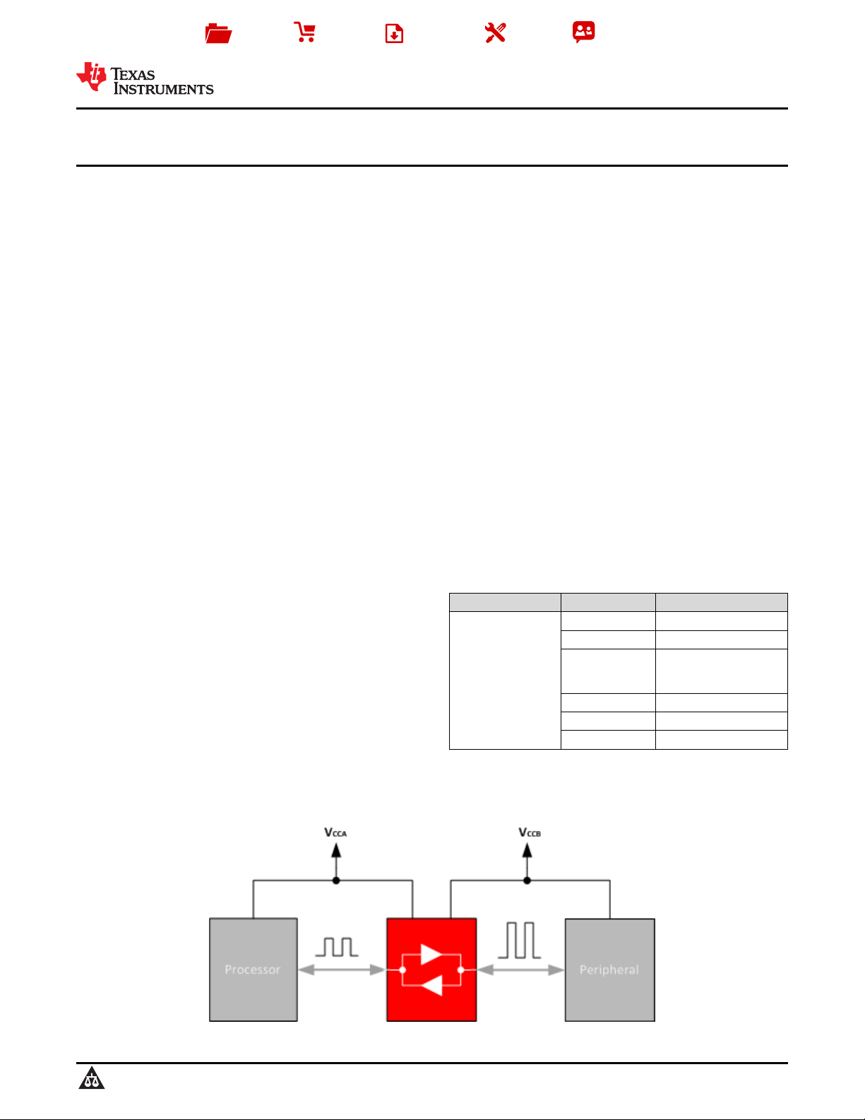
This 4-bit non-inverting translator uses two separate
configurable power-supply rails. The A port is
designed to track V
CCA
. V
accepts any supply
CCA
voltage from 1.2 V to 3.6 V. The B port is designed to
track V
CCB
. V
accepts any supply voltage from
CCB
1.65 V to 5.5 V. This allows for universal low-voltage
bidirectional translation between any of the 1.2-V,
1.5-V, 1.8-V, 2.5-V, 3.3-V, and 5-V voltage nodes.
V
should not exceed V
CCA
CCB
.
When the output-enable (OE) input is low, all outputs
are placed in the high-impedance state. To ensure
the high-impedance state during power up or power
down, OE should be tied to GND through a pulldown
resistor; the minimum value of the resistor is
determined by the current-sourcing capability of the
driver.
The TXB0104 is designed so that the OE input circuit
is supplied by V
CCA
.
This device is fully specified for partial-power-down
applications using I
. The I
off
circuitry disables the
off
outputs, preventing damaging current backflow
through the device when it is powered down.
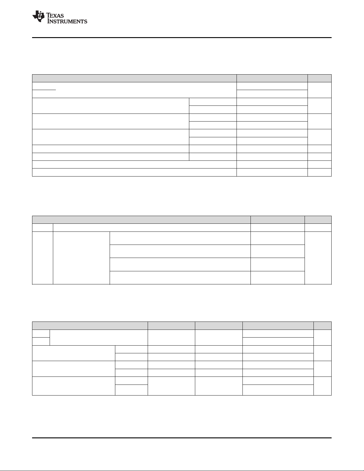
Device Information
PART NUMBER PACKAGE BODY SIZE (NOM)
UQFN (12) 2.00 mm x 1.70 mm
SOIC (14) 8.65 mm x 3.91 mm
BGA
TXB0104
(1) For all available packages, see the orderable addendum at
the end of the datasheet.
MICROSTAR 2.00 mm x 2.50 mm
JUNIOR (12)
TSSOP (14) 5.00 mm x 4.40 mm
VQFN (14) 3.50 mm x 3.50 mm
DSBGA (12) 1.40 mm x 1.90 mm
(1)
Typical Application Block Diagram for TXB010X
1
An IMPORTANT NOTICE at the end of this data sheet addresses availability, warranty, changes, use in safety-critical applications,
intellectual property matters and other important disclaimers. PRODUCTION DATA.
TXB0104
SCES650G –APRIL 2006–REVISED NOVEMBER 2014
www.ti.com
Table of Contents
1 Features.................................................................. 1
2 Applications ........................................................... 1
3 Description ............................................................. 1
4 Revision History..................................................... 2
5 Pin Configuration and Functions......................... 3
6 Specifications......................................................... 5
6.1 Absolute Maximum Ratings ..................................... 5
6.2 Handling Ratings....................................................... 5
6.3 Recommended Operating Conditions....................... 5
6.4 Thermal Information.................................................. 6
6.5 Electrical Characteristics .......................................... 6
6.6 Timing Requirements: V
6.7 Timing Requirements: V
6.8 Timing Requirements: V
6.9 Timing Requirements: V
6.10 Timing Requirements: V
6.11 Switching Characteristics: V
6.12 Switching Characteristics: V
6.13 Switching Characteristics: V
6.14 Switching Characteristics: V
6.15 Switching Characteristics: V
= 1.2 V ......................... 7
CCA
= 1.5 V ± 0.1 V ............ 7
CCA
= 1.8 V ± 0.15 V .......... 7
CCA
= 2.5 V ± 0.2 V ............ 7
CCA
= 3.3 V ± 0.3 V .......... 8 12 Device and Documentation Support ................. 19
CCA
= 1.2 V ................. 8 12.1 Trademarks........................................................... 19
CCA
= 1.5 V ± 0.1 V .... 8 12.2 Electrostatic Discharge Caution............................ 19
CCA
= 1.8 V ± 0.15 V .. 8 12.3 Glossary................................................................ 19
CCA
= 2.5 V ± 0.2 V .... 9
CCA
= 3.3 V ± 0.3 V .... 9
CCA
6.16 Operating Characteristics...................................... 10
6.17 Typical Characteristics.......................................... 11
7 Parameter Measurement Information ................ 12
8 Detailed Description ............................................ 13
8.1 Overview................................................................. 13
8.2 Functional Block Diagram ....................................... 13
8.3 Feature Description................................................. 14
8.4 Device Functional Modes........................................ 15
9 Application and Implementation ........................ 16
9.1 Application Information............................................ 16
9.2 Typical Application ................................................. 16
10 Power Supply Recommendations ..................... 18
11 Layout................................................................... 18
11.1 Layout Guidelines ................................................. 18
11.2 Layout Example .................................................... 18
13 Mechanical, Packaging, and Orderable
Information........................................................... 19
4 Revision History
NOTE: Page numbers for previous revisions may differ from page numbers in the current version.
Changes from Revision F (March 2012) to Revision G Page
• Added Pin Configuration and Functions section, Handling Rating table, Feature Description section, Device
Functional Modes, Application and Implementation section, Power Supply Recommendations section, Layout
section, Device and Documentation Support section, and Mechanical, Packaging, and Orderable Information
section ................................................................................................................................................................................... 1
Changes from Revision E (February 2010) to Revision F Page
• Added notes to pin out graphics............................................................................................................................................. 3
2 Submit Documentation Feedback Copyright © 2006–2014, Texas Instruments Incorporated
Product Folder Links: TXB0104
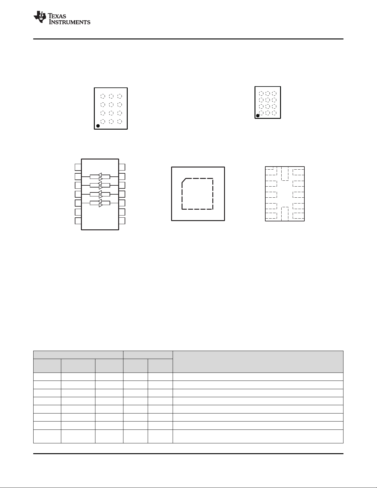
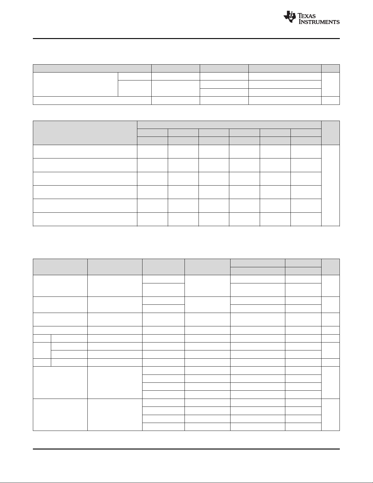
14
13
12
11
10
9
8
1
2
3
4
5
6
7
OE
D OR PW PACKAGE
(TOP VIEW)
GND
NC
A4
A3
A2
V
CCA
NC
B4
B3
B2
B1
V
CCB
A1
RGY PACKAGE
Exposed
Center
Pad
(TOP VIEW)
1 14
7 8
2
3
4
5
6
13
12
11
10
9
B1
B2
B3
B4
NC
A1
A2
A3
A4
NC
OE
V
CCB
GND
V
CCA
V
CCB
B1
B2
B3
RUT PACKAGE
(TOP VIEW)
3
2
6
10
1
4
8
9
11
12
A2
A3
V
CCA
A1
OE
GND
B4
5
7
A4
GXU/ZXU PACKAGE
(TOP VIEW)
4
3
2
1
A B C
YZT PACKAGE
(TOP VIEW)
D
C
B
A
3
2
1
www.ti.com
5 Pin Configuration and Functions
TXB0104
SCES650G –APRIL 2006–REVISED NOVEMBER 2014
A. N.C. − No internal connection
B. For RGY, if the exposed center pad is used, it must only be connected as a secondary ground or left
electrically open.
C. Pullup resistors are not required on both sides for Logic I/O.
D. If pull up or pull down resistors are needed, the resistor value must be over 50 kΩ.
E. 50 kΩ is a safe recommended value, if the customer can accept higher VOLor lower VOH, smaller pullup or
pulldown resistor is allowed, the draft estimation is VOL= V
RDW/(4.5 k + RDW).
F. If pullup resistors are needed, please refer to the TXS0104 or contact TI.
G. For detailed information, please refer to application note SCEA043.
NAME RUT NO. YZT NO.
Copyright © 2006–2014, Texas Instruments Incorporated Submit Documentation Feedback 3
× 4.5 k/(4.5 k + RPU) and VOH= V
CCOUT
Pin Functions
PIN BALL
.
FUNCTION
CCA
.
CCA
.
CCA
.
CCA
.
CCA
≤ 3.6 V and V
D, PW, OR GXU/
RGY NO. ZXU NO.
V
CCA
A1 2 2 A1 A3 Input/output 1. Referenced to V
A2 3 3 A2 B3 Input/output 2. Referenced to V
A3 4 4 A3 C3 Input/output 3. Referenced to V
A4 5 5 A4 D3 Input/output 4. Referenced to V
NC 6 – – – No connection. Not internally connected.
GND 7 6 B4 D2 Ground
OE 8 12 B3 C2
1 1 B2 B2 A-port supply voltage 1.2 V ≤ V
3-state output-mode enable. Pull OE low to place all outputs in 3-state
mode. Referenced to V
Product Folder Links: TXB0104
CCA
CCA
≤ V
CCB
CCOUT
.
×
TXB0104
SCES650G –APRIL 2006–REVISED NOVEMBER 2014
Pin Functions (continued)
PIN BALL
NAME RUT NO. YZT NO.
D, PW, OR GXU/
RGY NO. ZXU NO.
NC 9 – – – No connection. Not internally connected.
B4 10 7 C4 D1 Input/output 4. Referenced to V
B3 11 8 C3 C1 Input/output 3. Referenced to V
B2 12 9 C2 B1 Input/output 2. Referenced to V
B1 13 10 C1 A1 Input/output 1. Referenced to V
V
CCB
14 11 B1 A2 B-port supply voltage 1.65 V ≤ V
Pin Assignments (GXU / ZXU Package)
A B C
4 A4 GND B4
3 A3 OE B3
2 A2 V
1 A1 V
CCA
CCB
Pin Assignments (YZT Package)
3 2 1
D A4 GND B4
C A3 OE B3
B A2 V
A A1 V
CCA
CCB
FUNCTION
.
CCB
.
CCB
.
CCB
.
CCB
≤ 5.5 V.
CCB
www.ti.com
B2
B1
B2
B1
4 Submit Documentation Feedback Copyright © 2006–2014, Texas Instruments Incorporated
Product Folder Links: TXB0104
www.ti.com
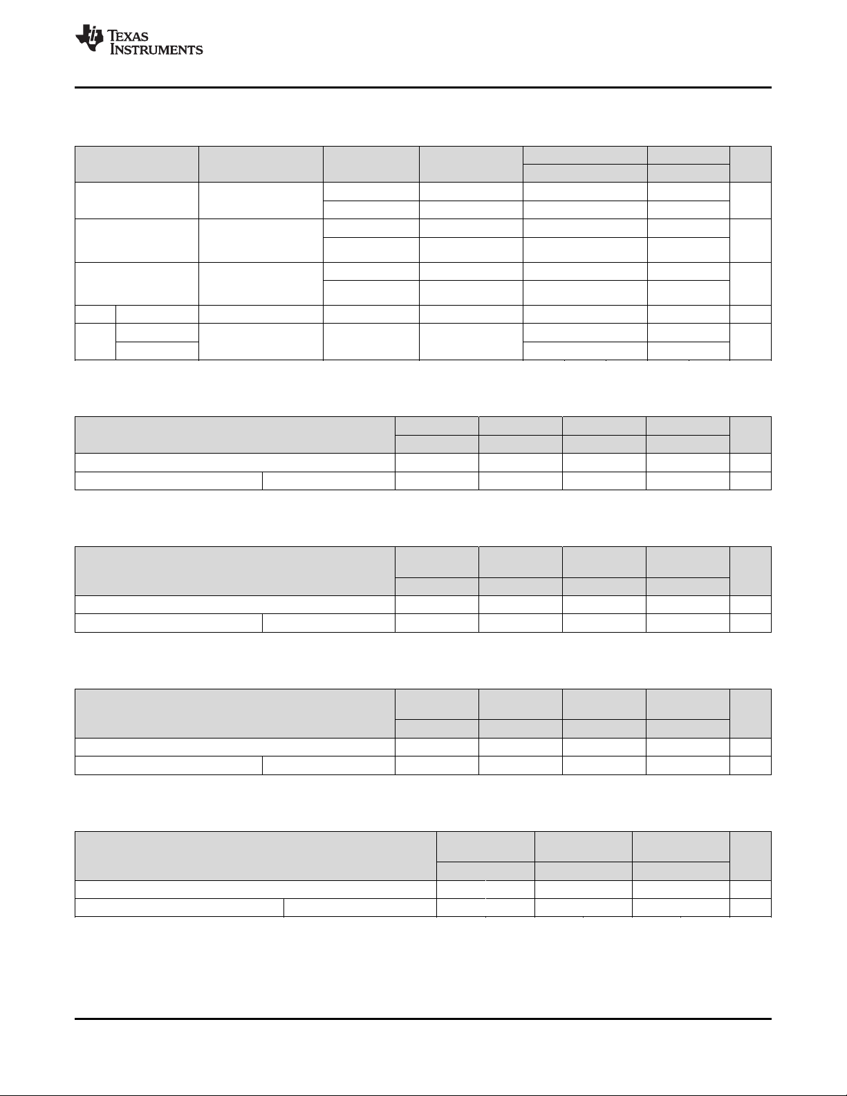
6 Specifications
TXB0104
SCES650G –APRIL 2006–REVISED NOVEMBER 2014
6.1 Absolute Maximum Ratings
(1)
over operating free-air temperature range (unless otherwise noted)
MIN MAX UNIT
V
CCA
V
CCB
V
I
V
O
V
O
I
IK
I
OK
I
O
Supply voltage range V
Input voltage range V
Voltage range applied to any output in the high-impedance or
power-off state
Voltage range applied to any output in the high or low
(2)
state
A port –0.5 4.6
B port –0.5 6.5
A port –0.5 4.6
B port -0.5 6.5
A port –0.5 V
B port –0.5 V
Input clamp current VI< 0 –50 mA
Output clamp current VO< 0 –50 mA
Continuous output current –50 50 mA
Continuous current through V
CCA
, V
, or GND –100 100 mA
CCB
–0.5 4.6
–0.5 6.5
CCA
CCB
+ 0.5
+ 0.5
V
V
(1) Stresses beyond those listed under Absolute Maximum Ratings may cause permanent damage to the device. These are stress ratings
only, and functional operation of the device at these or any other conditions beyond those indicated under Recommended Operating
Conditions is not implied. Exposure to absolute-maximum-rated conditions for extended periods may affect device reliability.
(2) The value of V
CCA
and V
are provided in the recommended operating conditions table.
CCB
6.2 Handling Ratings
MIN MAX UNIT
T
V
(1) JEDEC document JEP155 states that 500-V HBM allows safe manufacturing with a standard ESD control process.
(2) JEDEC document JEP157 states that 250-V CDM allows safe manufacturing with a standard ESD control process.
Storage temperature range –65 150 °C
stg
Human body model (HBM), per ANSI/ESDA/JEDEC JS-001, all
(1)
pins
, A Port
Human body model (HBM), per ANSI/ESDA/JEDEC JS-001, all
(1)
pins
Electrostatic discharge V
(ESD)
, B Port
Charged device model (CDM), per JEDEC specification
JESD22-C101, all pins
Charged device model (CDM), per JEDEC specification
JESD22-C101, all pins
(2)
, A Port
(2)
, B Port
–15 15
2.5
1.5
1.5
6.3 Recommended Operating Conditions
over operating free-air temperature range (unless otherwise noted)
V
CCA
V
CCA
Supply voltage V
V
CCB
V
High-level input voltage V
IH
V
Low-level input voltage V
IL
Voltage range applied to any A-port 0 3.6
V
output in the high-impedance 1.2 V to 3.6 V 1.65 V to 5.5 V V
O
or power-off state
(1) The A and B sides of an unused data I/O pair must be held in the same state, i.e., both at V
(2) V
(3) V
Copyright © 2006–2014, Texas Instruments Incorporated Submit Documentation Feedback 5
must be less than or equal to V
CCA
is the supply voltage associated with the input port.
CCI
Data inputs 1.2 V to 3.6 V 1.65 V to 5.5 V V
OE 1.2 V to 3.6 V 1.65 V to 5.5 V V
Data inputs 1.2 V to 5.5 V 1.65 V to 5.5 V 0 V
OE 1.2 V to 3.6 V 1.65 V to 5.5 V 0 V
B-port 0 5.5
and must not exceed 3.6 V.
CCB
Product Folder Links: TXB0104
(1)(2)
V
CCB
× 0.65
CCI
CCA
or both at GND.
CCI
MIN MAX UNIT
1.2 3.6
1.65 5.5
(3)
V
CCI
× 0.65 5.5
(3)
× 0.35
CCI
× 0.35
CCA
TXB0104
SCES650G –APRIL 2006–REVISED NOVEMBER 2014
www.ti.com
Recommended Operating Conditions (continued)
over operating free-air temperature range (unless otherwise noted)
V
CCA
Input transition
Δt/Δv 1.65 V to 3.6 V 40 ns/V
rise or fall rate
T
Operating free-air temperature –40 85 °C
A
A-port inputs 1.2 V to 3.6 V 1.65 V to 5.5 V 40
B-port inputs 1.2 V to 3.6 V
(1)(2)
V
CCB
MIN MAX UNIT
4.5 V to 5.5 V 30
6.4 Thermal Information
TXB0104
THERMAL METRIC
R
R
R
ψ
ψ
R
Junction-to-ambient thermal
θJA
resistance
Junction-to-case (top) thermal
θJC(top)
resistance
Junction-to-board thermal
θJB
resistance
Junction-to-top characterization
JT
parameter
Junction-to-board characterization
JB
parameter
Junction-to-case (bottom) thermal
θJC(bot)
resistance
(1) For more information about traditional and new thermal metrics, see the IC Package Thermal Metrics application report, SPRA953.
(1)
D GXU/ZXU PW RGY RUT YZT UNIT
14 PINS 12 PINS 14 PINS 14 PINS 12 PINS 12 PINS
90.7 127.1 121.0 52.8 119.8 89.2
50.5 92.8 50.0 67.7 42.6 0.9
45.4 62.2 62.8 28.9 52.5 14.4
°C/W
14.7 2.3 6.4 2.6 0.7 3.0
45.1 62.2 62.2 29.0 52.3 14.4
─ ─ ─ ─ ─ ─
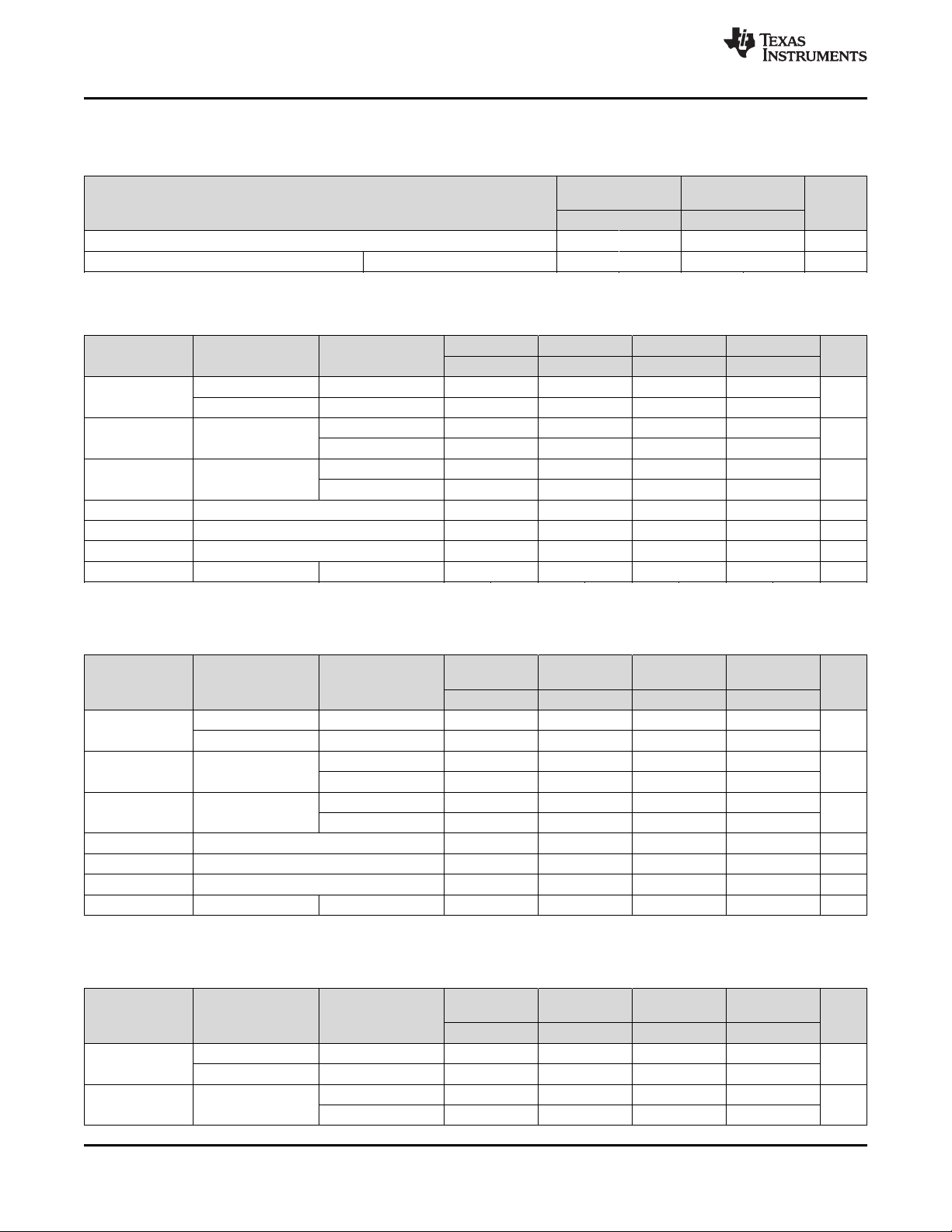
6.5 Electrical Characteristics
(1)(2)
over recommended operating free-air temperature range (unless otherwise noted)
PARAMETER TEST CONDITIONS V
CCA
1.2 V 1.1
V
OHA
V
OLA
V
OHB
V
OLB
I
OE VI= V
I
A port VIor VO= 0 to 3.6 V 0 V 0 V to 5.5 V –1 1 –2 2
I
off
B port VIor VO= 0 to 5.5 V 0 V to 3.6 V 0 V –1 1 –2 2
I
A or B port OE = GND 1.2 V to 3.6 V 1.65 V to 5.5 V –1 1 –2 2 μA
OZ
IOH= –20 μA V
IOL= 20 μA V
1.4 V to 3.6 V
1.2 V 0.3
1.4 V to 3.6 V 0.4
IOH= –20 μA 1.65 V to 5.5 V V
IOL= 20 μA 1.65 V to 5.5 V 0.4 V
or GND 1.2 V to 3.6 V 1.65 V to 5.5 V –1 1 –2 2 μA
CCI
1.2 V 1.65 V to 5.5 V 0.06
I
CCA
VI= V
IO= 0
CCI
or GND,
1.4 V to 3.6 V 1.65 V to 5.5 V 5
3.6 V 0 V 2
0 V 5.5 V –2
1.2 V 1.65 V to 5.5 V 3.4
I
CCB
VI= V
IO= 0
CCI
or GND,
1.4 V to 3.6 V 1.65 V to 5.5 V 5
3.6 V 0 V –2
0 V 5.5 V 2
V
CCB
TA= 25°C –40°C to 85°C
MIN TYP MAX MIN MAX
V
CCA
– 0.4
V
CCB
– 0.4
UNIT
μA
μA
μA
(1) V
(2) V
is the supply voltage associated with the input port.
CCI
is the supply voltage associated with the output port.
CCO
6 Submit Documentation Feedback Copyright © 2006–2014, Texas Instruments Incorporated
Product Folder Links: TXB0104
www.ti.com
TXB0104
SCES650G –APRIL 2006–REVISED NOVEMBER 2014
Electrical Characteristics
(1)(2)
(continued)
over recommended operating free-air temperature range (unless otherwise noted)
PARAMETER TEST CONDITIONS V
I
CCA
+ I
CCB
VI= V
IO= 0
VI= V
I
CCZA
IO= 0, μA
OE = GND
VI= V
I
CCZB
C
OE 1.2 V to 3.6 V 1.65 V to 5.5 V 3 4 pF
i
A port 5 6
C
io
B port 11 14
IO= 0, μA
OE = GND
6.6 Timing Requirements: V
TA= 25°C, V
CCA
= 1.2 V
or GND,
CCI
or GND, 1.2 V 1.65 V to 5.5 V 0.05
CCI
or GND, 1.2 V 1.65 V to 5.5 V 3.3
CCI
CCA
Data rate 20 20 20 20 Mbps
t
Pulse duration Data inputs 50 50 50 50 ns
w
CCA
1.2 V 1.65 V to 5.5 V 3.5
1.4 V to 3.6 V 1.65 V to 5.5 V 10
1.4 V to 3.6 V 1.65 V to 5.5 V 5
1.4 V to 3.6 V 1.65 V to 5.5 V 5
1.2 V to 3.6 V 1.65 V to 5.5 V pF
= 1.2 V
V
CCB
V
CCB
= 1.8 V V
CCB
TYP TYP TYP TYP
TA= 25°C –40°C to 85°C
MIN TYP MAX MIN MAX
= 2.5 V V
= 3.3 V V
CCB
CCB
= 5 V
UNIT
μA
UNIT
6.7 Timing Requirements: V
= 1.5 V ± 0.1 V
CCA
over recommended operating free-air temperature range, V
Data rate 40 40 40 40 Mbps
t
Pulse duration Data inputs 25 25 25 25 ns
w
6.8 Timing Requirements: V
= 1.8 V ± 0.15 V
CCA
over recommended operating free-air temperature range, V
Data rate 60 60 60 60 Mbps
t
Pulse duration Data inputs 17 17 17 17 ns
w
6.9 Timing Requirements: V
= 2.5 V ± 0.2 V
CCA
over recommended operating free-air temperature range, V
Data rate 100 100 100 Mbps
t
Pulse duration Data inputs 10 10 10 ns
w
= 1.5 V ± 0.1 V (unless otherwise noted)
CCA
V
= 1.8 V V
CCB
± 0.15 V ± 0.2 V ± 0.3 V ± 0.5 V
= 2.5 V V
CCB
= 3.3 V V
CCB
CCB
= 5 V
MIN MAX MIN MAX MIN MAX MIN MAX
= 1.8 V ± 0.15 V (unless otherwise noted)
CCA
V
= 1.8 V V
CCB
± 0.15 V ± 0.2 V ± 0.3 V ± 0.5 V
= 2.5 V V
CCB
= 3.3 V V
CCB
CCB
= 5 V
MIN MAX MIN MAX MIN MAX MIN MAX
= 2.5 V ± 0.2 V (unless otherwise noted)
CCA
V
= 2.5 V V
CCB
± 0.2 V ± 0.3 V ± 0.5 V
= 3.3 V V
CCB
CCB
= 5 V
MIN MAX MIN MAX MIN MAX
UNIT
UNIT
UNIT
Copyright © 2006–2014, Texas Instruments Incorporated Submit Documentation Feedback 7
Product Folder Links: TXB0104
TXB0104
SCES650G –APRIL 2006–REVISED NOVEMBER 2014
www.ti.com
6.10 Timing Requirements: V
over recommended operating free-air temperature range, V
= 3.3 V ± 0.3 V
CCA
= 3.3 V ± 0.3 V (unless otherwise noted)
CCA
V
= 3.3 V V
CCB
± 0.3 V ± 0.5 V
CCB
= 5 V
MIN MAX MIN MAX
Data rate 100 100 Mbps
t
w
6.11 Switching Characteristics: V
TA= 25°C, V
PARAMETER UNIT
Pulse duration Data inputs 10 10 ns
= 1.2 V
CCA
= 1.2 V
CCA
V
t
t
t
trA, t
trB, t
t
SK(O)
= 1.8 V V
FROM TO
(INPUT) (OUTPUT)
CCB
TYP TYP TYP TYP
A B 6.9 5.7 5.3 5.5
pd
en
dis
fA
fB
B A 7.4 6.4 6 5.8
OE μs
OE ns
A 1 1 1 1
B 1 1 1 1
A 18 15 14 14
B 20 17 16 16
A-port rise and fall times 4.2 4.2 4.2 4.2 ns
B-port rise and fall times 2.1 1.5 1.2 1.1 ns
Channel-to-channel skew 0.4 0.5 0.5 1.4 ns
= 2.5 V V
CCB
= 3.3 V V
CCB
CCB
= 5 V
Max data rate 20 20 20 20 Mbps
UNIT
ns
6.12 Switching Characteristics: V
over recommended operating free-air temperature range, V
PARAMETER UNIT
t
pd
t
en
t
dis
trA, t
fA
trB, t
fB
t
SK(O)
FROM TO
(INPUT) (OUTPUT)
A B 1.4 12.9 1.2 10.1 1.1 10 0.8 9.9
B A 0.9 14.2 0.7 12 0.4 11.7 0.3 13.7
OE μs
OE ns
A-port rise and fall times 1.4 5.1 1.4 5.1 1.4 5.1 1.4 5.1 ns
B-port rise and fall times 0.9 4.5 0.6 3.2 0.5 2.8 0.4 2.7 ns
Channel-to-channel skew 0.5 0.5 0.5 0.5 ns
= 1.5 V ± 0.1 V
CCA
= 1.5 V ± 0.1 V (unless otherwise noted)
CCA
V
= 1.8 V V
CCB
± 0.15 V ± 0.2 V ± 0.3 V ± 0.5 V
= 2.5 V V
CCB
= 3.3 V V
CCB
CCB
= 5 V
MIN MAX MIN MAX MIN MAX MIN MAX
A 1 1 1 1
B 1 1 1 1
A 5.9 31 5.7 25.9 5.6 23 5.7 22.4
B 5.4 30.3 4.9 22.8 4.8 20 4.9 19.5
Max data rate 40 40 40 40 Mbps
6.13 Switching Characteristics: V
over recommended operating free-air temperature range, V
PARAMETER UNIT
t
pd
t
en
FROM TO
(INPUT) (OUTPUT)
A B 1.6 11 1.4 7.7 1.3 6.8 1.2 6.5
B A 1.5 12 1.3 8.4 1 7.6 0.9 7.1
OE μs
= 1.8 V ± 0.15 V
CCA
= 1.8 V ± 0.15 V (unless otherwise noted)
CCA
V
= 1.8 V V
CCB
± 0.15 V ± 0.2 V ± 0.3 V ± 0.5 V
= 2.5 V V
CCB
= 3.3 V V
CCB
CCB
= 5 V
MIN MAX MIN MAX MIN MAX MIN MAX
A 1 1 1 1
B 1 1 1 1
ns
ns
8 Submit Documentation Feedback Copyright © 2006–2014, Texas Instruments Incorporated
Product Folder Links: TXB0104
www.ti.com
TXB0104
SCES650G –APRIL 2006–REVISED NOVEMBER 2014
Switching Characteristics: V
over recommended operating free-air temperature range, V
PARAMETER UNIT
t
dis
trA, t
fA
trB, t
fB
t
SK(O)
FROM TO
(INPUT) (OUTPUT)
OE ns
A-port rise and fall times 1 4.2 1.1 4.1 1.1 4.1 1.1 4.1 ns
B-port rise and fall times 0.9 3.8 0.6 3.2 0.5 2.8 0.4 2.7 ns
Channel-to-channel skew 0.5 0.5 0.5 0.5 ns
= 1.8 V ± 0.15 V (continued)
CCA
= 1.8 V ± 0.15 V (unless otherwise noted)
CCA
V
= 1.8 V V
CCB
± 0.15 V ± 0.2 V ± 0.3 V ± 0.5 V
MIN MAX MIN MAX MIN MAX MIN MAX
A 5.9 31 5.1 21.3 5 19.3 5 17.4
B 5.4 30.3 4.4 20.8 4.2 17.9 4.3 16.3
= 2.5 V V
CCB
= 3.3 V V
CCB
CCB
= 5 V
Max data rate 60 60 60 60 Mbps
6.14 Switching Characteristics: V
over recommended operating free-air temperature range, V
PARAMETER UNIT
t
pd
t
en
t
dis
trA, t
fA
trB, t
fB
t
SK(O)
FROM TO
(INPUT) (OUTPUT)
A B 1.1 6.3 1 5.2 0.9 4.7
B A 1.2 6.6 1.1 5.1 0.9 4.4
OE μs
OE ns
A-port rise and fall times 0.8 3 0.8 3 0.8 3 ns
B-port rise and fall times 0.7 2.6 0.5 2.8 0.4 2.7 ns
Channel-to-channel skew 0.5 0.5 0.5 ns
= 2.5 V ± 0.2 V
CCA
= 2.5 V ± 0.2 V (unless otherwise noted)
CCA
V
= 2.5 V V
CCB
± 0.2 V ± 0.3 V ± 0.5 V
= 3.3 V V
CCB
MIN MAX MIN MAX MIN MAX
A 1 1 1
B 1 1 1
A 5.1 21.3 4.6 15.2 4.6 13.2
B 4.4 20.8 3.8 16 3.9 13.9
CCB
= 5 V
Max data rate 100 100 100 Mbps
ns
6.15 Switching Characteristics: V
over recommended operating free-air temperature range, V
PARAMETER UNIT
t
pd
t
en
t
dis
trA, t
fA
trB, t
fB
t
SK(O)
FROM TO
(INPUT) (OUTPUT)
A B 0.9 4.7 0.8 4
B A 1 4.9 0.9 3.8
OE μs
OE ns
A-port rise and fall times 0.7 2.5 0.7 2.5 ns
B-port rise and fall times 0.5 2.1 0.4 2.7 ns
Channel-to-channel skew 0.5 0.5 ns
= 3.3 V ± 0.3 V
CCA
= 3.3 V ± 0.3 V (unless otherwise noted)
CCA
V
= 3.3 V V
CCB
± 0.3 V ± 0.5 V
CCB
= 5 V
MIN MAX MIN MAX
A 1 1
B 1 1
A 4.6 15.2 4.3 12.1
B 3.8 16 3.4 13.2
ns
Max data rate 100 100 Mbps
Copyright © 2006–2014, Texas Instruments Incorporated Submit Documentation Feedback 9
Product Folder Links: TXB0104
TXB0104
SCES650G –APRIL 2006–REVISED NOVEMBER 2014
6.16 Operating Characteristics
TA= 25°C
V
CCA
1.2 V 1.2 V 1.5 V 1.8 V 2.5 V 2.5 V 3.3 V
V
PARAMETER TEST CONDITIONS UNIT
5 V 1.8 V 1.8 V 1.8 V 2.5 V 5 V to
TYP TYP TYP TYP TYP TYP TYP
A-port input, B-port output 7.8 10 9 8 8 8 9
C
pdA
B-port input, A-port output 12 11 11 11 11 11 11
A-port input, B-port output 38.1 28 28 28 29 29 29
C
pdB
B-port input, A-port output 25.4 19 18 18 19 21 22
A-port input, B-port output 0.01 0.01 0.01 0.01 0.01 0.01 0.01
C
pdA
B-port input, A-port output 0.01 0.01 0.01 0.01 0.01 0.01 0.01
A-port input, B-port output 0.01 0.01 0.01 0.01 0.01 0.01 0.03
C
pdB
B-port input, A-port output 0.01 0.01 0.01 0.01 0.01 0.01 0.04
CL= 0, f = 10 MHz,
tr= tf= 1 ns,
OE = V
(outputs enabled)
CCA
CL= 0, f = 10 MHz,
tr= tf= 1 ns,
OE = GND
(outputs disabled)
CCB
www.ti.com
3.3 V
5 V
pF
pF
10 Submit Documentation Feedback Copyright© 2006–2014, Texas Instruments Incorporated
Product Folder Links: TXB0104
www.ti.com
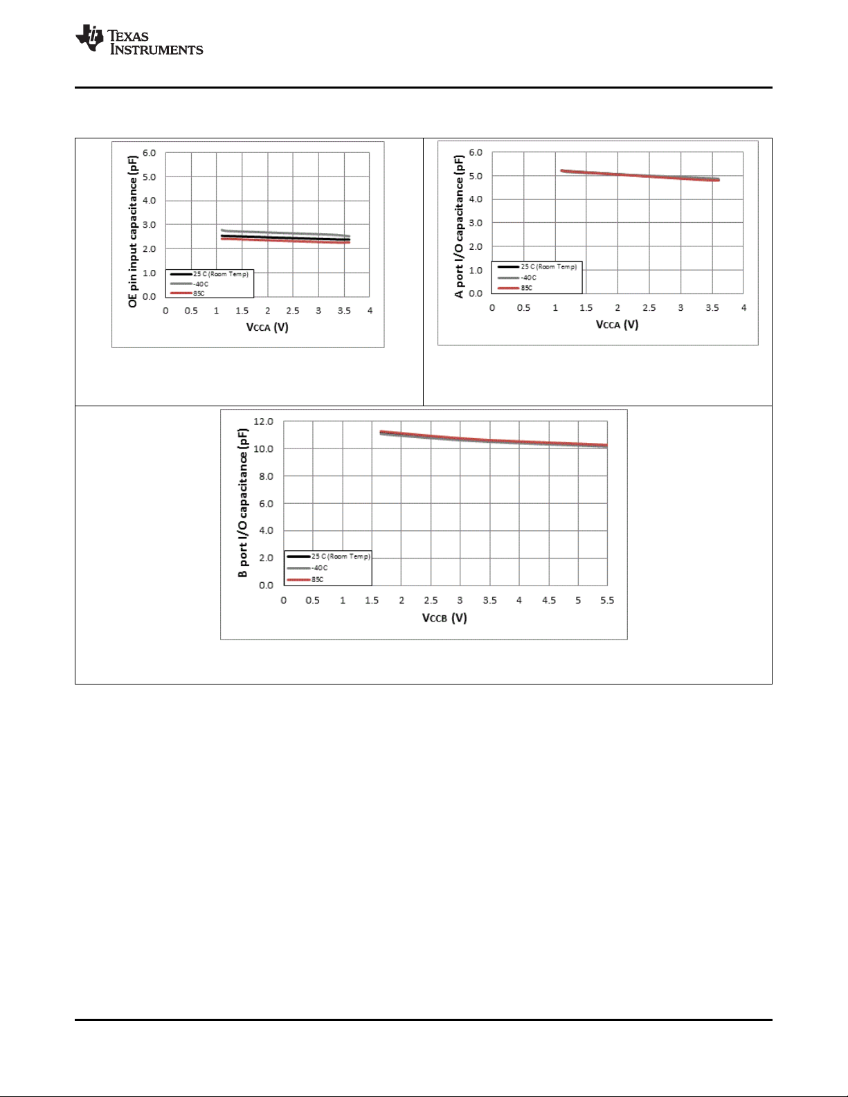
6.17 Typical Characteristics
V
= 3.3 V
CCB
Figure 1. Input capacitance for OE pin (CI) vs Power Supply
(V
)
CCA
TXB0104
SCES650G –APRIL 2006–REVISED NOVEMBER 2014
V
= 3.3 V
CCB
Figure 2. Capacitance for A port I/O pins (CiO) vs Power
Supply (V
CCA
)
V
= 1.8 V
CCA
Figure 3. Capacitance for B port I/O pins (CiO) vs Power Supply (V
Copyright © 2006–2014, Texas Instruments Incorporated Submit Documentation Feedback 11
CCB
)
Product Folder Links: TXB0104
 Loading...