
www.DataSheet4U.com
VSB/QAM Receiver
Data Manual
TVP9900
Literature Number: SLEA064
March 2007
PRODUCTION DATA information is current as of publication date.
Products conform to specifications per the terms of the Texas
Instruments standard warranty. Production processing does not
necessarily include testing of all parameters.

www.ti.com
TVP9900
VSB/QAM Receiver
SLEA064 – MARCH 2007
Contents
1 Introduction ......................................................................................................................... 7
1.1 Features ....................................................................................................................... 7
1.2 Ordering Information ........................................................................................................ 7
2 Block Diagram ..................................................................................................................... 8
3 Terminal Assignments .......................................................................................................... 9
3.1 Pinout .......................................................................................................................... 9
3.2 Terminal Functions ......................................................................................................... 10
4 Functional Description ........................................................................................................ 12
4.1 Analog Front End ........................................................................................................... 12
4.2 VSB/QAM Demodulator ................................................................................................... 12
4.3 Forward Error Correction .................................................................................................. 12
4.4 Output Formatter ........................................................................................................... 13
4.5 I
4.6 Tuner Control Interface .................................................................................................... 17
4.7 Antenna Control Interface ................................................................................................. 19
4.8 General-Purpose IO (GPIO) .............................................................................................. 21
4.9 Clock Circuits ............................................................................................................... 22
4.10 Power-Up Sequence ....................................................................................................... 22
4.11 Reset ......................................................................................................................... 22
4.12 Power Down ................................................................................................................ 23
4.13 Power-Supply Voltage Requirements ................................................................................... 23
5 High-K PCB Design Recommendations ................................................................................. 24
6 Host Processor I
6.1 Overview ..................................................................................................................... 25
6.2 I
2
C Host Interface .......................................................................................................... 14
4.5.1 I
4.5.2 I
4.6.1 Tuner Write Operation .......................................................................................... 18
4.6.2 Tuner Read Operation .......................................................................................... 18
4.7.1 Antenna Interrogation/Initialization ............................................................................ 20
4.7.2 Transmit Data to Antenna Operation ......................................................................... 21
4.7.3 Receive Data from Antenna Operation ....................................................................... 21
2
C Register Definitions .................................................................................................... 27
6.2.1 Receiver Control Register 1 / Soft Reset ..................................................................... 27
6.2.2 Receiver Control Register 2 .................................................................................... 28
6.2.3 VSB Control Register ........................................................................................... 28
6.2.4 AGC Control Register ........................................................................................... 29
6.2.5 VSB FEC Time Counter Register 1 ........................................................................... 29
6.2.6 VSB FEC Time Counter Register 2 ........................................................................... 30
6.2.7 VSB FEC Time Counter Register 3 ........................................................................... 30
6.2.8 QAM FEC Time Counter Register 1 .......................................................................... 31
6.2.9 QAM FEC Time Counter Register 2 .......................................................................... 31
6.2.10 QAM FEC Time Counter Register 3 .......................................................................... 31
6.2.11 VSB FEC Segment Error Count Threshold Register 1 ..................................................... 32
6.2.12 VSB FEC Segment Error Count Threshold Register 2 ..................................................... 32
6.2.13 Update Status Control Register ............................................................................... 32
6.2.14 Receiver Status Register ....................................................................................... 33
6.2.15 AGC Status Register 1 .......................................................................................... 33
6.2.16 AGC Status Register 2 .......................................................................................... 33
6.2.17 AGC Status Register 3 .......................................................................................... 34
6.2.18 NTSC Rejection Filter Status Register ....................................................................... 34
2
C Write Operation ............................................................................................. 15
2
C Read Operation ............................................................................................. 16
2
C Register Summary .................................................................................. 25
Contents 2 Submit Documentation Feedback

www.ti.com
TVP9900
VSB/QAM Receiver
SLEA064 – MARCH 2007
6.2.19 Timing Recovery Status Register 1 ........................................................................... 34
6.2.20 Timing Recovery Status Register 2 ........................................................................... 34
6.2.21 Timing Recovery Status Register 3 ........................................................................... 35
6.2.22 Timing Recovery Status Register 4 ........................................................................... 35
6.2.23 Timing Recovery Status Register 5 ........................................................................... 35
6.2.24 Timing Recovery Status Register 6 ........................................................................... 35
6.2.25 Pilot Tracking Status Register 1 ............................................................................... 36
6.2.26 Pilot Tracking Status Register 2 ............................................................................... 36
6.2.27 Pilot Tracking Status Register 3 ............................................................................... 36
6.2.28 Carrier Recovery Status Register 1 ........................................................................... 36
6.2.29 Carrier Recovery Status Register 2 ........................................................................... 37
6.2.30 Carrier Recovery Status Register 3 ........................................................................... 37
6.2.31 Carrier Recovery Status Register 4 ........................................................................... 37
6.2.32 Carrier Recovery Status Register 5 ........................................................................... 37
6.2.33 Carrier Recovery Status Register 6 ........................................................................... 38
6.2.34 FEC Status Register 1 .......................................................................................... 38
6.2.35 FEC Status Register 2 .......................................................................................... 39
6.2.36 FEC Status Register 3 .......................................................................................... 39
6.2.37 FEC Status Register 4 .......................................................................................... 39
6.2.38 GPIO Alternate Function Select Register .................................................................... 40
6.2.39 GPIO Output Data Register .................................................................................... 40
6.2.40 GPIO Output Enable Register ................................................................................. 41
6.2.41 GPIO Input Data Register ...................................................................................... 41
6.2.42 MPEG Interface Output Enable Register 1 .................................................................. 42
6.2.43 MPEG Interface Output Enable Register 2 .................................................................. 43
6.2.44 Tuner Control Interface – I
6.2.45 Tuner Control Interface – Data Register 1 Through 8 ...................................................... 43
6.2.46 Tuner Control Interface – Control and Status Register ..................................................... 44
6.2.47 Antenna Control Interface – Control and Status Register .................................................. 44
6.2.48 Antenna Control Interface – Transmit Data Register 1 ..................................................... 45
6.2.49 Antenna Control Interface – Transmit Data Register 2 ..................................................... 45
6.2.50 Antenna Control Interface – Receive Data Register 1 ...................................................... 45
6.2.51 Antenna Control Interface – Receive Data Register 2 ...................................................... 46
6.2.52 Firmware ID – ROM Version Register ........................................................................ 46
6.2.53 Firmware ID – RAM Major Version Register ................................................................. 46
6.2.54 Firmware ID – RAM Minor Version Register ................................................................. 46
6.2.55 Device ID LSB Register ........................................................................................ 47
6.2.56 Device ID MSB Register ........................................................................................ 47
6.2.57 Miscellaneous Control Register ................................................................................ 47
6.2.58 Software Interrupt Raw Status Register ...................................................................... 48
6.2.59 Software Interrupt Status Register ............................................................................ 48
6.2.60 Software Interrupt Mask Register ............................................................................. 49
6.2.61 Software Interrupt Clear Register ............................................................................. 50
7 Electrical Specifications ...................................................................................................... 51
7.1 Absolute Maximum Ratings ............................................................................................... 51
7.2 Recommended Operating Conditions ................................................................................... 52
7.3 DC Electrical Characteristics ............................................................................................. 52
7.4 Analog Input Characteristics .............................................................................................. 53
7.5 Timing Characteristics ..................................................................................................... 54
7.5.1 Crystal and Input Clock ......................................................................................... 54
7.5.2 Device Reset ..................................................................................................... 54
7.5.3 MPEG Interface .................................................................................................. 55
7.5.3.1 Parallel Mode (Data Only) ...................................................................................... 55
2
C Slave Device Address Register ............................................ 43
Contents 3

www.ti.com
TVP9900
VSB/QAM Receiver
SLEA064 – MARCH 2007
7.5.3.2 Serial Mode (Data Only) ........................................................................................ 56
7.5.3.3 Parallel Mode (Data With Redundancy) ...................................................................... 57
7.5.3.4 Serial Mode (Data With Redundancy) ........................................................................ 58
7.5.4 Host and Tuner I
8 Application Circuit .............................................................................................................. 60
2
C Interface .................................................................................. 59
Contents 4 Submit Documentation Feedback

www.ti.com
TVP9900
VSB/QAM Receiver
SLEA064 – MARCH 2007
List of Figures
2-1 TVP9900 Block Diagram .......................................................................................................... 8
4-1 Parallel Transport Stream Timing Diagram (Data Only) ..................................................................... 13
4-2 Serial Transport Stream Timing Diagram (Data Only) ....................................................................... 13
4-3 Parallel Transport Stream Timing Diagram (Data + Redundancy) ......................................................... 14
4-4 Serial Transport Stream Timing Diagram (Data + Redundancy) ........................................................... 14
4-5 Tuner Control Interface System ................................................................................................. 17
4-6 Antenna Control Interface System .............................................................................................. 19
4-7 25-MHz Crystal Oscillation ....................................................................................................... 22
4-8 4-MHz Clock Input ................................................................................................................ 22
5-1 Thermal Land Size and Via Array ............................................................................................... 24
7-1 Crystal or Clock Timing Waveform ............................................................................................. 54
7-2 Device Reset Signal Timing Waveforms ....................................................................................... 54
7-3 MPEG Interface – Parallel Mode (Data Only) Timing Waveforms .......................................................... 55
7-4 MPEG Interface – Serial Mode (Data Only) Timing Waveforms ............................................................ 56
7-5 MPEG Interface – Parallel Mode (Data With Redundancy) Timing Waveforms .......................................... 57
7-6 MPEG Interface – Serial Mode (Data with Redundancy) Timing Waveforms ............................................. 58
7-7 I
7-8 I
2
C SCL and SDA Timing Waveforms .......................................................................................... 59
2
C Start and Stop Conditions Timing Waveforms ............................................................................ 59
List of Figures 5

www.ti.com
TVP9900
VSB/QAM Receiver
SLEA064 – MARCH 2007
List of Tables
3-1 Terminal Functions ................................................................................................................ 10
4-1 MPEG-2 Transport Stream Interface ........................................................................................... 13
4-2 MPEG-2 Transport Stream Output Clock Frequency ........................................................................ 14
4-3 I
4-4 I
4-5 I
4-6 Tuner Control Interface Registers ............................................................................................... 17
4-7 Antenna Control Interface Registers ............................................................................................ 19
4-8 Antenna Control Interface Pins .................................................................................................. 20
6-1 I
7-1 Crystal and Input Clock Timing .................................................................................................. 54
7-2 Device Reset Timing .............................................................................................................. 54
7-3 Parallel Mode (Data Only) Timing .............................................................................................. 55
7-4 Serial Mode (Data Only) Timing ................................................................................................. 56
7-5 Parallel Mode (Data With Redundancy) Timing ............................................................................... 57
7-6 Serial Mode (Data With Redundancy) Timing ................................................................................. 58
7-7 Host and Tuner I
2
C Terminal Description ......................................................................................................... 15
2
C Host Interface Device Write Addresses .................................................................................... 15
2
C Host Interface Device Read Address ...................................................................................... 16
2
C Host Interface Registers ..................................................................................................... 25
2
C Interface Timing .......................................................................................... 59
6 List of Tables Submit Documentation Feedback

www.ti.com
1 Introduction
The TVP9900 is a cost-effective digital TV (DTV) front-end IC targeted for low-cost high-volume DTV
receivers. The TVP9900 is a system-on-chip (SoC) device that integrates the main functions of a DTV
front-end system, including programmable gain amplifier (PGA), A/D converter, VSB demodulator, ATSC
forward error correction (FEC), QAM demodulator, and ITU-T Annex B FEC. It provides rich peripheral
support including AGC control, tuner control, CEA-909 antenna control, and host I2C interface. The
TVP9900 supports processing of ATSC VSB or ITU-T Annex B QAM IF inputs.
1.1 Features
• ATSC 8-VSB Demodulation and FEC
• ITU-J.83B Compliant 64/256 QAM
Demodulation and FEC
• Direct 44-MHz IF Sampling Eliminates Need for
External Downconverter
• Integrated IF PGA
• Integrated High-Speed 10-bit A/D Converter
• Integrated Digital Filter Relaxes External Tuner
Filters
• Sigma-Delta DAC for AGC Control
• Adjacent Channel Filter
• NTSC Co-Channel Rejection Filter
• All Digital Timing Recovery
• Pilot Tracking Loop With Lock Status Indicator
Signal
• Decision-Directed Carrier Phase Tracking
Loop
• Field and Segment Synchronization With Sync
Status Indicator Signal
TVP9900
VSB/QAM Receiver
SLEA064 – MARCH 2007
• Host Interrupt for Remote Monitoring of Signal
Quality
• SNR Monitor
• BER Monitor
• Integrated De-Interleaver RAM
• Parallel/Serial MPEG Output Interface With
Error Packet Indicator
• Direct Tuner Control Interface
• EIA/CEA-909 Antenna Control Interface
• Option for 4-MHz Clock Input Driven by MOP
IC in Tuner, So No Quartz Crystal Required for
Demodulator
• External DAC and VCXO for Clock Recovery
Not Required
• Equalizer Covers Echo Profile Required by
ATSC A.74 Guideline
• Superior Multipath Performance Demodulating
for Brazil Ensembles A Through E
• Power-Down Mode
• 80-Pin TQFP Package
1.2 Ordering Information
T
A
0 ° C to 70 ° C
(1) For the most current package and ordering information, see the Package Option Addendum at the end of this document, or see the TI
Web site at www.ti.com .
Please be aware that an important notice concerning availability, standard warranty, and use in critical applications of Texas
Instruments semiconductor products and disclaimers thereto appears at the end of this document.
PRODUCTION DATA information is current as of publication date.
Products conform to specifications per the terms of the Texas
Instruments standard warranty. Production processing does not
necessarily include testing of all parameters.
(1)
PACKAGED DEVICES
80-Pin TQFP-PowerPAD
TVP9900PFP Tray
TVP9900PFPR Tape and Reel
Copyright © 2007, Texas Instruments Incorporated
PACKAGE OPTION
www.ti.com
VSB/QAM
Demodulator
ITU-T J.83
Annex B FEC
ATSC FEC
I2CSDA
I2CSCL
TUNSDA
TUNSCL
AIFIN_P
AIFIN_N
Tuner
Interface
AGCOUT
GPIO [7:0]
Output
Formatter
CEA-909
Interface
GPIO
Interface
ANTCNTLIO
VBUS
ROM RAM
MCU
Host
Interface
Interrupt Ctrl
JTAG
DCLK
BYTE_START
PACCLK
DATAOUT[7:0]
DERROR
PLL
INTREQ
PWRDOWN
AFE
VSB/QAM
Demodulator
ITU-T J.83
Annex B FEC
ATSC FEC
AIFIN_P
AIFIN_N
Tuner
Interface
AGCOUT
GPIO [7:0]
XTALIN
XTALOUT
CLKIN
CLKSEL
CLKOUT
Output
Formatter
CEA-909
Interface
GPIO
Interface
VBUS
ROM RAM
Host
Interface
Interrupt Ctrl
JTAG
DCLK
BYTE_START
PACCLK
DATAOUT[7:0]
DERROR
PLL
TVP9900
VSB/QAM Receiver
SLEA064 – MARCH 2007
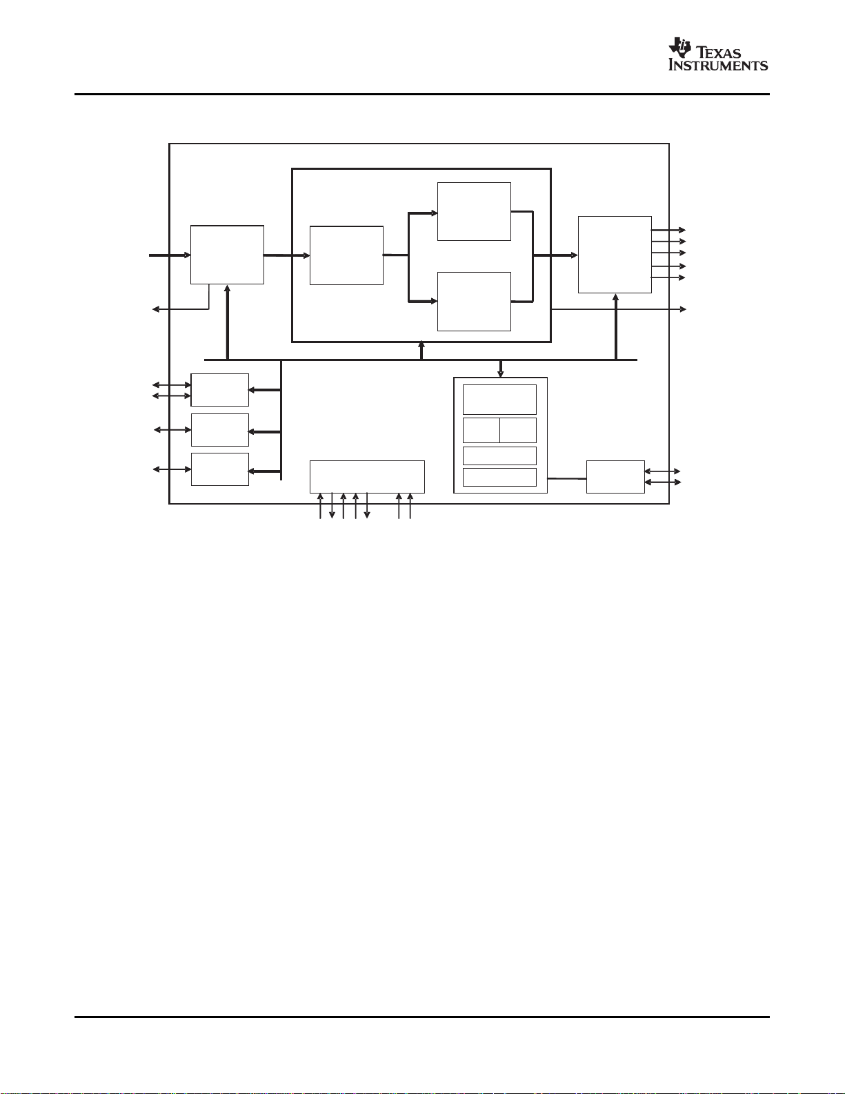
2 Block Diagram
Figure 2-1. TVP9900 Block Diagram
8 Block Diagram Submit Documentation Feedback

www.ti.com
3 Terminal Assignments
TVP9900
80-PinTQFP
(TopView)
1
AGND
2
AVDD_3_3
3
AIFIN_P
4
AIFIN_N
5
AVDD_3_3
6
AGND
7
AVDD_1_5
8
AGND
9
AGND_PLL
10
AVDD_PLL_1_5
11
XTALOUT
12
XTALREF
13
XTALIN
14
CLKIN
15
DIVINSEL
16
CLKOUT
17
DGND
18
DVDD_1_5
19
IOGND
20
IOVDD_3_3
21
RESETZ
22
TMSEL0
23
TMSEL1
24
DGND
25
D
VDD_1_5
26
TMSEL2
27
TMSEL3
28
A
GCOUT
29
ANTCNTLIO
30
TUNSDA
31
TUNSCL
32
IOGND
33
IOVDD_3_3
34
I2CSDA
35
I2CSCL
36
DGND
37
DVDD_1_5
38
I2CA0
39
PWRD
WN
40
DERROR
60
59
58
57
56
55
54
53
52
51
50
49
48
47
46
45
44
43
42
41
DATAOUT0
DATAOUT1
DVDD_1_5
DGND
DATAOUT2
DATAOUT3
DATAOUT4
IOVDD_3_3
IOGND
DATAOUT5
DATAOUT6
DATAOUT7/SERDATA0
DVDD_1_5
DGND
PACCLK
BYTESTART
IOVDD_3_3
IOGND
DCLK
DGND
80
79
78
77
76
75
74
73
72
71
70
69
68
67
66
65
64
63
62
61
NSUB
BGREFCAP
BIASRES
AVDD_REF_3_3
AGND_REF
AGND
DGND
DVDD_1_5
GPIO0/ANTCNTLIN
GPIO1
GPIO2
DGND
DVDD_1_5
GPIO3
GPIO4
GPIO5/SYNCOUT
IO
VDD_3_3
IOGND
GPIO6
GPIO7/INTREQ
3.1 Pinout
TVP9900
VSB/QAM Receiver
SLEA064 – MARCH 2007
Submit Documentation Feedback Terminal Assignments 9

www.ti.com
TVP9900
VSB/QAM Receiver
SLEA064 – MARCH 2007
3.2 Terminal Functions
Table 3-1. Terminal Functions
TERMINAL
NAME NO.
IF INTERFACE
AIFIN_P 3 I Analog positive differential IF input
AIFIN_N 4 I Analog negative differential IF input
TRANSPORT STREAM INTERFACE
DCLK 42 O MPEG-2 data clock output
BYTE_START 45 O
PACCLK 46 O
DERROR 40 O data output packet. Indicates an error in the input data. This pin should be tied low if not
DATAOUT7/SERDATA0 49 O
50, 51,
DATAOUT[6:0] O MPEG-2 parallel data output bits 6-0.
CLOCK SIGNALS
XTALIN 13 I a crystal. When using an external clock source, a 4 MHz or 25 MHz clock must be used.
XTALOUT 11 O Crystal output. Output from the on-chip oscillator to an external crystal.
XTALREF 12 I
CLKIN 14 I Test clock input. For normal operation, this input should be tied low.
DIVINSEL 15 I
CLKOUT 16 O Test clock output. For normal operation, this output is not used.
MISCELLANEOUS SIGNALS
AGCOUT 28 O AGC control Delta-Sigma DAC output.
ANTCNTLIO 29 I/O Smart antenna control interface input/output.
TUNSDA 30 I/O Tuner I2C serial data input/output. NOTE: The output functions as an open-drain.
TUNSCL 31 I/O Tuner I2C serial clock. NOTE: The output functions as an open-drain.
GPIO7/INTREQ 61 I/O
GPIO6 62 I/O
GPIO5/SYNCOUT 65 I/O
GPIO[4:2] I/O General purpose I/O
GPIO1 71 O
54, 55,
56, 59,
60
66, 67,
70
I/O DESCRIPTION
MPEG-2 Byte Start signal. An active high output signal that indicates the first byte of a
transport stream data packet.
MPEG-2 interface packet framing signal. An active high output signal that remains high
for the entire length of the valid data packet.
MPEG-2 interface data error. An active high output signal that indicates an error in the
in use.
1. MPEG-2 parallel data output. Bit 7 is the first bit of the transport stream.
2. MPEG-2 serial data output
Crystal input. Input to the on-chip oscillator from an external crystal. The required crystal
frequency is 25 MHz. This input can also be driven by an external clock source instead of
NOTE: If an external clock source is used, the input can only be used with 1.5-V signal
levels.
External crystal reference. This pin is used for the external crystal capacitor ground
reference.
PLL VCO divider default input select. This input is used to select the default VCO divider
value for the PLL. If a 25-MHz crystal or clock is used for XTALIN, then DIVINSEL should
be driven low. If a 4-MHz crystal or clock is used for XTALIN, then DIVINSEL should be
driven high.
1. General purpose I/O
2. Interrupt request output
1. General purpose I/O
2. Reserved
1. General purpose I/O
2. Sync output
Dedicated to Smart Antenna support. Outputs direction of signal on pin 29 in Smart
Antenna 1-pin mode.
0 = Signal input from antenna to TVP9900, pin 29
1 = Signal output from TVP9900 pin 29 to antenna
Terminal Assignments10 Submit Documentation Feedback

www.ti.com
VSB/QAM Receiver
Table 3-1. Terminal Functions (continued)
TERMINAL
NAME NO.
GPIO0/ANTCNTLIN 72 I/O
RESETZ 21 I
PWRDOWN 39 I Power down terminal. An active high signal puts the device in a low power state.
TMSEL[3:0] I Test mode select. Tie low for normal operation.
HOST INTERFACE
I2CSDA 34 I/O Host I2C serial data input/output. NOTE: The pin functions as an open-drain output.
I2CSCL 35 I/O Host I2C serial clock. NOTE: The pin functions as an open-drain output.
I2CA0 38 I address.
POWER SUPPLIES
DVDD_1_5 P Digital power supply. Connect to 1.5-V digital supply.
DGND P Digital power supply return. Connect to digital ground.
IOVDD_3_3 44, 53, P IO power supply. Connect to 3.3-V digital supply.
IOGND 43, 52, P IO power supply return. Connect to digital ground.
AVDD_3_3 2, 5 P Analog power supply. Connect to 3.3-V analog supply.
AVDD_1_5 7 P Analog power supply. Connect to 1.5-V analog supply.
AGND P Analog power supply return. Connect to analog ground.
AVDD_PLL_1_5 10 P PLL power supply. Connect to 1.5-V analog supply.
AGND_PLL 9 P PLL power supply return. Connect to analog ground.
NSUB 80 P Die substrate. Connect to PCB ground.
AVDD_REF_3_3 77 P Analog reference power supply. Connect to 3.3-V analog supply.
AGND_REF 76 P Analog reference ground. Connect to analog ground.
BGREFCAP 79 O Band-gap reference capacitor connection
BIASRES 78 O Analog bias register. Connect through a 24-k Ω resistor to PCB ground.
22, 23,
26, 27
18, 25,
37, 48,
58, 68,
73
17, 24,
36, 41,
47, 57,
69, 74
20, 33,
64
19, 32,
63
1, 6, 8,
75
I/O DESCRIPTION
1. General purpose I/O
2. Antenna Control Input
System reset. An active-low asynchronous input that initializes the device to the default
state.
Host I2C device address select. Determines address for I2C (sampled during reset). A
pullup or pulldown 10-k Ω resistor is needed to program the terminal to the desired
0 = Address is 0xB8h
1 = Address is 0xBAh
TVP9900
SLEA064 – MARCH 2007
Submit Documentation Feedback Terminal Assignments 11

www.ti.com
TVP9900
VSB/QAM Receiver
SLEA064 – MARCH 2007
4 Functional Description
4.1 Analog Front End
The TVP9900 receiver has an analog input channel that accepts one differential or single-ended 44-MHz
center frequency IF input, which are ac-coupled. The receiver supports a maximum input differential
voltage range of 1 Vpp with PGA setting at unity gain. The programmable gain amplifier (PGA) and the
AGC circuit work together and ensure that the input signal is amplified sufficiently to ensure the proper
input range for the ADC. The ADC has 10 bits of resolution. The clock input for the ADC comes from the
PLL. An external downconverter is not required to use this IF direct sampling method. The analog front
end and adjacent digital filter can potentially relax the requirement for external analog filters, and only one
external SAW filter is required.
4.2 VSB/QAM Demodulator
The VSB/QAM demodulator is designed for 8-VSB demodulation compliant with ATSC, and 64/256 QAM
demodulation compliant with ITU-T J83 Annex B. The VSB/QAM demodulator in the TVP9900 is
composed of the following blocks:
• Automatic gain control
• Adjacent channel filter
• NTSC rejection filter
• Timing recovery
• Pilot tracking
• Matched filter
• Decision feedback equalizer
• Carrier recovery
The all-digital demodulator architecture does not require an external downconverter, AGC control DAC,
clock recovery VCXO, or carrier recovery VCXO. This architecture makes a low-cost system
implementation possible.
4.3 Forward Error Correction
Forward Error Correction (FEC) in the TVP9000 includes the following blocks:
• QAM FEC
• VSB FEC
The Trellis decoder is designed for help protect against short-burst interference. The VSB synchronizer
performs segment and frame synchronization and outputs the synchronization signal with data. An internal
RAM is shared by both VSB and QAM modes, and additional external RAM is not required.
– Trellis decoder
– Synchronizer
– De-randomizer
– De-interleaver
– Reed Solomon decoder
– MPEG deframer
– Trellis decoder
– Synchronizer
– De-interleaver
– Reed Solomon decoder
– De-randomizer
Functional Description12 Submit Documentation Feedback
www.ti.com
4.4 Output Formatter
DCLK
DATAOUT[7:0]
BYTE_START
PACCLK
Data 188 bytes
DCLK
DATAOUT[7:0]
BYTE_START
PACCLK
Data 188 bytes
Data 188 bytes
7 6 5 4 3 2 1 0
7 6 1 0
1stbyte
7 6 5 4 3 2 1 0
7 6
DCLK
DATAOUT[7:0]
BYTE_START
PACCLK
Data 188 bytes
7 6 5 4 3 2 1 0
7 6 1 0
1stbyte
7 6 5 4 3 2 1 0
7 6
DCLK
DATAOUT[7:0]
BYTE_START
PACCLK
The TVP9900 transport stream interfaces directly to the back-end IC, which provides transport stream
compliance with ISO/IEC 13818-1 in parallel or serial modes. The details of the transport stream interface
are shown in Table 4-1 . In serial mode, DATAOUT[7] is used as the serial data output, with the MSB
output first. The maximum output rate is 42.1 Mbit/s in serial mode. The polarity of DCLK, BYTE_START,
DERROR, and PACCLK is programmable.
Table 4-1. MPEG-2 Transport Stream Interface
TERMINAL TYPE DESCRIPTION
DCLK O Parallel/serial clock output
Parallel/serial data output
DATAOUT[7:0] O DATAOUT7 is the first bit of the transport stream in parallel mode.
DATAOUT7 is the serial data output in serial mode.
BYTE_START O Packet sync, indicates the start byte of a transport packet
PACCLK O Packet enable, indicates the valid packet data
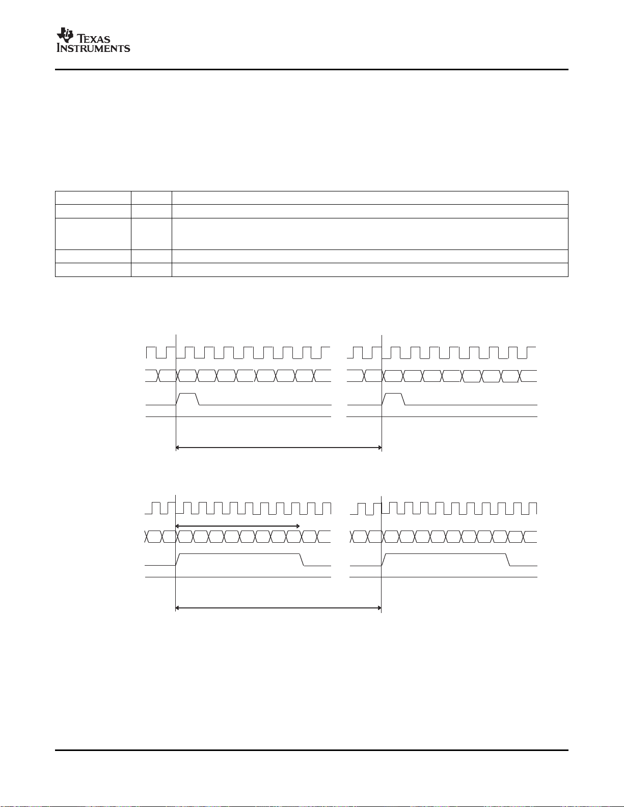
Figure 4-1 and Figure 4-2 show the parallel and serial transport stream timing diagrams in data-only
mode. In data-only mode, 188 bytes of data is transferred from the transport stream interface
continuously. PACCLK is always kept high.
TVP9900
VSB/QAM Receiver
SLEA064 – MARCH 2007
Figure 4-1. Parallel Transport Stream Timing Diagram (Data Only)
Figure 4-2. Serial Transport Stream Timing Diagram (Data Only)
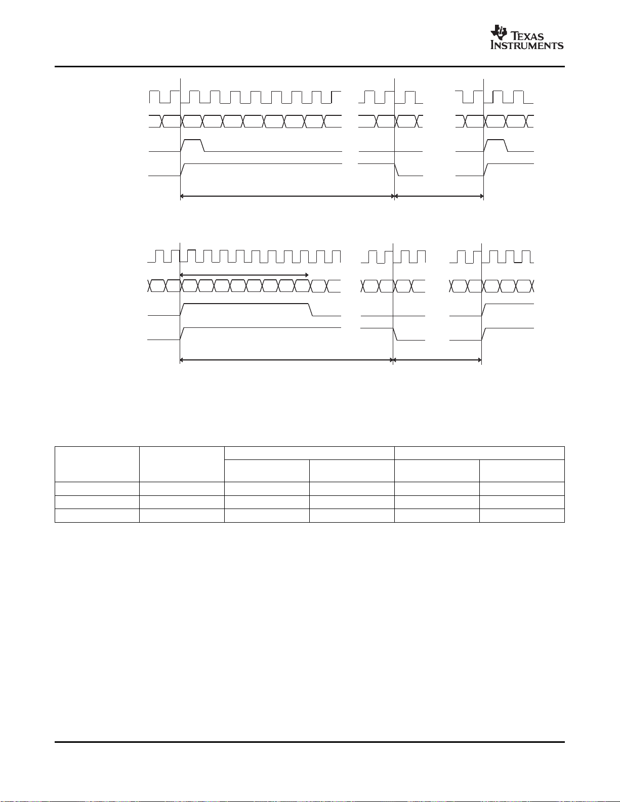
Figure 4-3 and Figure 4-4 show the parallel and serial transport stream timing diagrams in data and
redundancy mode. In data and redundancy mode, 188 bytes of data is transferred from the transport
stream interface with redundant data bytes. PACCLK only becomes high when the data is valid.
Redundancy data is 20 bytes in the ATSC standard and 16 bytes in ITU-T J.83 Annex B.
Submit Documentation Feedback Functional Description 13
www.ti.com
Parity 16 or 20 bytesData 188 bytes
DCLK
DATAOUT[7:0]
BYTE_START
PACCLK
Parity 16 or 20 bytesData 188 bytes
DCLK
DATAOUT[7:0]
BYTE_START
PACCLK
Data 188 bytes Parity 16 or 20 bytes
7 6 5 4 3 2 1 0
7 6 1 0 7 6 1 0 7 6 5
1stbyte
DCLK
DATAOUT[7:0]
BYTE_START
PACCLK
Data 188 bytes Parity 16 or 20 bytes
7 6 5 4 3 2 1 0
7 6 1 0 7 6 1 0 7 6 5
1stbyte
DCLK
DATAOUT[7:0]
BYTE_START
PACCLK
TVP9900
VSB/QAM Receiver
SLEA064 – MARCH 2007
Figure 4-3. Parallel Transport Stream Timing Diagram (Data + Redundancy)
Figure 4-4. Serial Transport Stream Timing Diagram (Data + Redundancy)
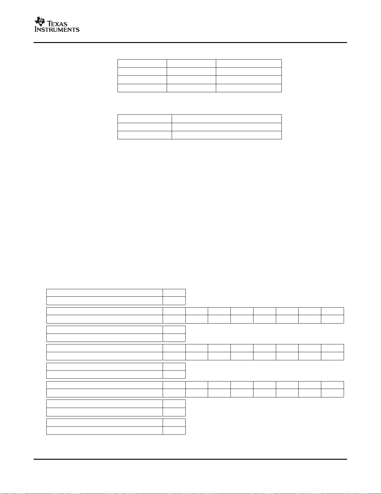
Table 4-2 shows the transport stream clock frequency in each mode.
Table 4-2. MPEG-2 Transport Stream Output Clock Frequency
MODE
8VSB 19.39266 19.39266 2.42408 21.45571 2.68196
64QAM 26.97035 26.97035 3.37129 29.26570 3.65821
256QAM 38.81070 38.81070 4.85133 42.11374 5.26422
BIT RATE
(Mbps)
SERIAL CLOCK PARALLEL CLOCK SERIAL CLOCK PARALLEL CLOCK
DATA ONLY DATA + REDUNDANCY
(MHz) (MHz) (MHz) (MHz)
4.5 I2C Host Interface
Communication with the TVP9900 receiver is via an I2C host interface. The I2C standard consists of two
signals, the serial input/output data (I2CSDA) line and the input/output clock line (I2CSCL), which carry
information between the devices connected to the bus. A 1-bit control signal (I2CA0) is used for slave
address selection. Although an I2C system can be multi-mastered, the TVP9900 can function as a slave
device only. Since I2CSDA and I2CSCL are kept open-drain at logic high output level or when the bus is
not driven, the user should connect I2CSDA and I2CSCL to IOVDD_3.3 via a pullup resistor on the board.
At the trailing edge of reset, the status of the I2CA0 line is sampled to determine the device address used.
Table 4-3 summarizes the terminal functions of the I2C-mode host interface. Table 4-4 and Table 4-5
show the device address selection options.
14 Functional Description Submit Documentation Feedback
www.ti.com
TVP9900
VSB/QAM Receiver
SLEA064 – MARCH 2007
Table 4-3. I2C Terminal Description
SIGNAL TYPE DESCRIPTION
I2CA0 I Slave address selection
I2CSCL I/O (open drain) Input/output clock line
I2CSDA I/O (open drain) Input/output data line
Table 4-4. I2C Host Interface Device Write Addresses
I2CA0 WRITE ADDRESS
0 B8h
1 BAh
Data transfer rate on the bus is up to 400 kbits/s. The number of interfaces connected to the bus is
dependent on the bus capacitance limit of 400 pF. The data on the SDA line must be stable during the
high period of the SCL, except for start and stop conditions. The high or low state of the data line can only
change with the clock signal on the SCL line being low. A high-to-low transition on the SDA line while the
SCL is high indicates an I2C start condition. A low-to-high transition on the SDA line while the SCL is high
indicates an I2C stop condition.
Every byte placed on the SDA must be 8 bits long. The number of bytes that can be transferred is
unrestricted. Each byte must be followed by an acknowledge bit. The acknowledge-related clock pulse is
generated by the I2C master.
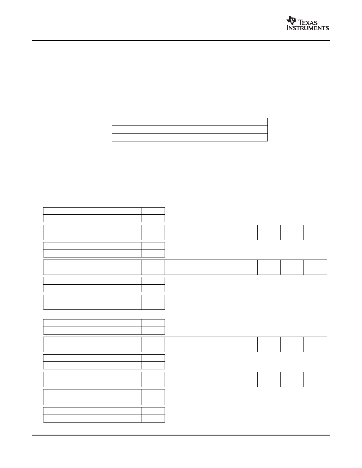
4.5.1 I2C Write Operation
Data transfers occur utilizing the following illustrated formats. An I2C master initiates a write operation to
the TVP9900 receiver by generating a start condition (S), followed by the TVP9900 I2C address (as shown
below), in MSB first bit order, followed by a 0 to indicate a write cycle. After receiving an acknowledge
from the TVP9900 receiver, the master presents the sub-address of the register or the first of a block of
registers it wants to write, followed by one or more bytes of data, MSB first. The TVP9900 receiver
acknowledges each byte after completion of each transfer. The I2C master terminates the write operation
by generating a stop condition (P).
Step 1 0
I2C Start (master)
Step 2 7 6 5 4 3 2 1 0
I2C General address (master)
Step 3 9
I2C Acknowledge (slave)
Step 4 7 6 5 4 3 2 1 0
I2C Write register address (master)
Step 5 9
I2C Acknowledge (slave)
Step 6 7 6 5 4 3 2 1 0
I2C Write data (master)
(1)
Step 7
I2C Acknowledge (slave)
Step 8 0
I2C Stop (master)
(1) Repeat steps 6 and 7 until all data have been written.
S
1 0 1 1 1 0 X 0
A
Addr Addr Addr Addr Addr Addr Addr Addr
A
Data Data Data Data Data Data Data Data
9
A
P
Submit Documentation Feedback Functional Description 15
www.ti.com
TVP9900
VSB/QAM Receiver
SLEA064 – MARCH 2007
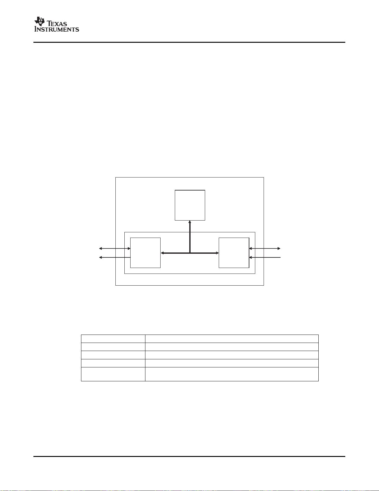
4.5.2 I2C Read Operation
The read operation consists of two phases. The first phase is the address phase. In this phase, an I2C
master initiates a write operation to the TVP9900 receiver by generating a start condition (S) followed by
the TVP9900 I2C address, in MSB first bit order, followed by a 0 to indicate a write cycle. After receiving
acknowledges from the TVP9900 receiver, the master presents the sub-address of the register or the first
of a block of registers it wants to read. After the cycle is acknowledged, the master terminates the cycle
immediately by generating a stop condition (P).
Table 4-5. I2C Host Interface Device Read Address
I2CA0 READ ADDRESS
0 B8h
1 BAh
The second phase is the data phase. In this phase, an I2C master initiates a read operation to the
TVP9900 receiver by generating a start condition, followed by the TVP9900 I2C address (as shown below
for a read operation), in MSB-first bit order, followed by a 1 to indicate a read cycle. After an acknowledge
from the TVP9900 receiver, the I2C master receives one or more bytes of data from the TVP9900
receiver. The I2C master acknowledges the transfer at the end of each byte. After the last data byte
desired has been transferred from the TVP9900 receiver to the master, the master generates a not
acknowledge, followed by a stop.
Read Phase 1
Step 1 0
I2C Start (master)
Step 2 7 6 5 4 3 2 1 0
I2C General address (master)
Step 3 9
I2C Acknowledge (slave)
Step 4 7 6 5 4 3 2 1 0
I2C Write register address (master)
Step 5 9
I2C Acknowledge (slave)
Step 6 0
I2C Stop (master)
Read Phase 2
Step 7 0
I2C Start (master)
Step 8 7 6 5 4 3 2 1 0
I2C General address (master)
Step 9 9
I2C Acknowledge (slave)
Step 10 7 6 5 4 3 2 1 0
I2C Read data (slave)
(1)
Step 11
I2C Not Acknowledge (master)
Step 12 0
I2C Stop (master)
(1) Repeat steps 10 and 11 for all bytes read. Master does not acknowledge the last read data received.
S
1 0 1 1 1 0 X 0
A
Addr Addr Addr Addr Addr Addr Addr Addr
A
P
S
1 0 1 1 1 0 X 0
A
Data Data Data Data Data Data Data Data
9
A
P
Functional Description16 Submit Documentation Feedback
www.ti.com
4.6 Tuner Control Interface
Tuner
Control
Interface
Host
I2C
Interface
MCU
From
Host
Processor
SDA
SCL
TUNSDA
TUNSCL
To
Tuner
Tuner
Control
Interface
Host
I2C
Interface
From
Host
Processor
SDA
SCL
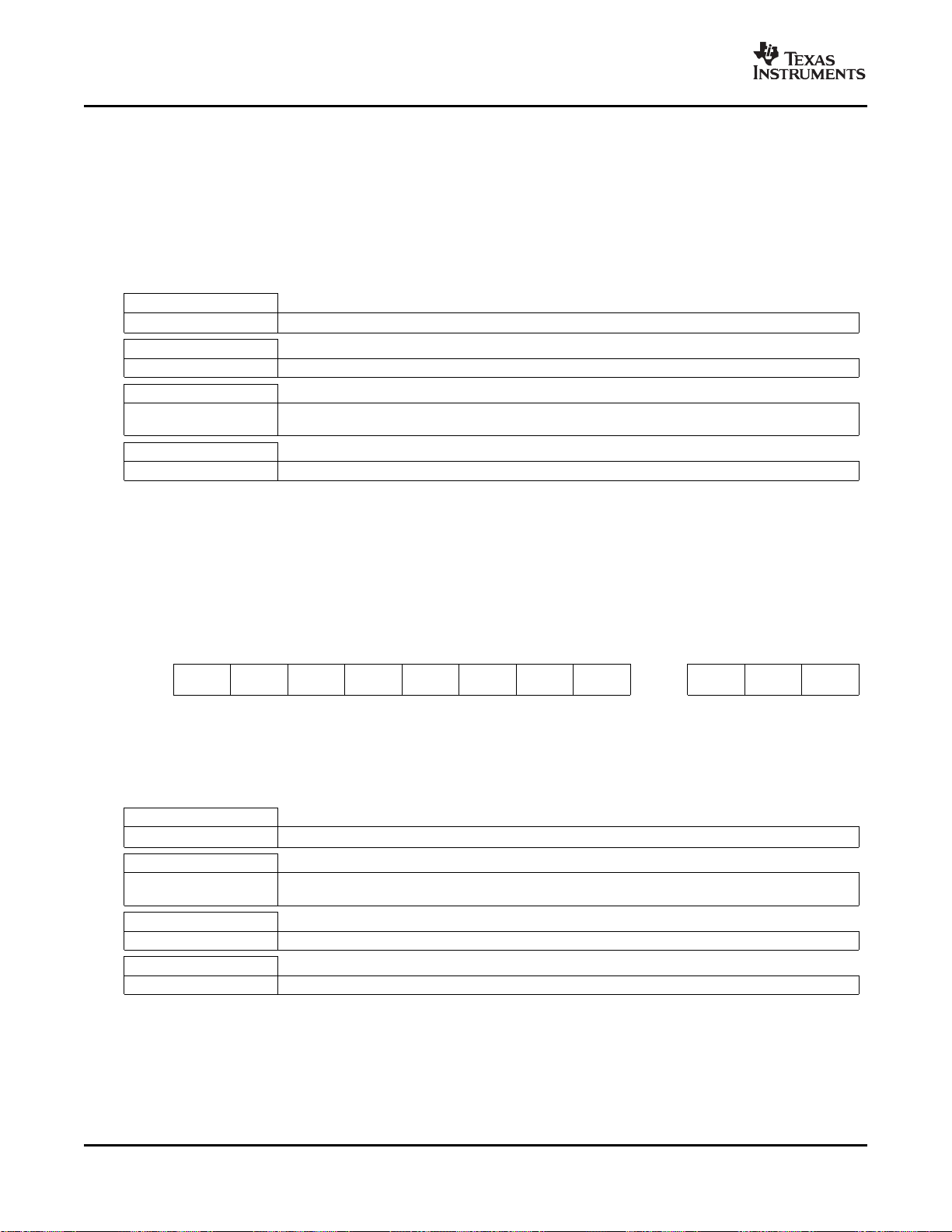
The TVP9900 has an I2C-compatible two-wire serial interface that can be used by the host processor for
tuner control. This dedicated tuner interface can be used by the host processor to transfer data to/from the
tuner in order to isolate the tuner from the main system I2C bus. As a result, noise coupling to the tuner
from host processor I2C bus transfers should be minimized.
The TVP9900 tuner control interface operates as an I2C bus master and supports both 100-kbps and
400-kbps data transfer rates. The mode and transfer rate is set in the Tuner Control Interface – Control
and Status Register (5Eh), bit 0. The device does not support a multi-master bus environment (bus
arbitration is not supported).
To transfer data to/from the tuner, the host processor first writes the transaction to a set of registers in the
TVP9900 via the host processor I2C interface. Then the TVP9900 internal MCU transfers the data to/from
the tuner via the tuner control interface.
TUNSCL and TUNSDA need to be pulled up to the 3.3-V supply (IOVDD) and not to a 5-V supply.
Figure 4-5 shows the block diagram of the tuner control interface system.
TVP9900
VSB/QAM Receiver
SLEA064 – MARCH 2007
Figure 4-5. Tuner Control Interface System
Table 4-6 lists the I2C registers and their functions used to control the tuner interface.
Table 4-6. Tuner Control Interface Registers
REGISTER FUNCTION
55h Tuner I2C slave address and R/W control
56h to 5Dh Data registers 1 through 8
5Eh Byte Count, Transaction Start, and I2C Mode
F9, FB, FD, FFh
Software Interrupt Raw Status, Status, Mask, and Clear – Transaction Error
and Done Status
When the TVP9900 tuner I2C interface is used, rather than controlling the tuner over the host processor
I2C bus interface, two status bits are provided in the TVP9900 to indicate a transaction error or the
completion of a successful transaction. The TCIERROR bit in the TVP9900 Software Interrupt Status
Register (FBh) gets set as a result of a transaction error. The TCIDONE bit in the same register gets set
at the end of a normal transaction; it does not get set for an abnormal transaction. The TVP9900 can be
configured so that setting the TCIERROR or TCODONE status bits can assert the INTREQ output of the
TVP9900; this requires the mask bits to be configured correctly in the TVP9900 Software Interrupt Mask
Register (FDh).
Submit Documentation Feedback Functional Description 17
www.ti.com
TVP9900
VSB/QAM Receiver
SLEA064 – MARCH 2007
If the host INTREQ is not used, the TCIDONE and TCIERROR interrupts should be masked and the host
should poll the TCIDONE status bit to determine when the transaction is complete, and the host should
poll the TCIERROR status bit to determine when an error has occurred.
Tuner data transfers occur utilizing the following illustrated formats.
4.6.1 Tuner Write Operation
The following steps are required to initiate a write operation to the tuner. The host processor first writes
the required transaction data to a set of registers in the TVP9900 via the host processor I2C interface.
Step 1
Register 55h
Step 2
Registers 56h to 5Dh Write data bytes to be sent to tuner; 56h is first byte sent
Step 3
Register 5Eh
Step 4
Register FBh Check state of bits 1:0 or INTREQ pin to verify successful transaction
Set tuner I2C slave address (bits 7:1) and read/write control (bit 0 = 0)
Set byte count (bits 7:5) and I2C mode (bit 0)
Set bit 2 to 1 to start transaction to tuner
After the transaction has been initiated, the TVP9900 internal MCU transfers the data to the tuner via the
tuner control interface. Acting as the I2C master, the TVP9900 initiates a write operation to the tuner (as
shown below), by generating a start condition, followed by the tuner I2C address, in MSB-first bit order,
followed by a 0 to indicate a write cycle. After receiving an acknowledge from the tuner, the TVP9900
presents the sub-address of the register, if needed, followed by one or more bytes of data, MSB first. The
tuner acknowledges each byte after completion of each transfer. The TVP9900 terminates the write
operation by generating a stop condition.
TVP9900/Tuner Write Operation
SDA Start W Ack Ack Data 1 Ack ... Data N Ack Stop
Device Base
Address Address
4.6.2 Tuner Read Operation
The following steps are required to initiate a read operation from the tuner. The host processor first writes
the required transaction data to a set of registers in the TVP9900 via the host processor I2C interface,
then reads the data bytes received from the tuner stored in TVP9900 registers.
Step 1
Register 55h
Step 2
Register 5Eh
Step 3
Register FBh Check state of bits 1:0 or INTREQ pin to verify successful transaction
Step 4
Registers 56h to 5Dh Read data bytes from tuner; 56h is first byte received
Set tuner I2C slave address (bits 7:1) and read/write control (bit 0 = 1)
Set byte count (bits 7:5) and I2C mode (bit 0)
Set bit 2 to 1 to start transaction to tuner
After the transaction has been initiated, the TVP9900 internal MCU transfers the data from the tuner via
the tuner control interface. The read operation consists of two phases, as shown below. The first phase is
the address phase. In this phase, the TVP9900 I2C master initiates a write operation to the tuner by
generating a start condition, followed by the tuner I2C address, in MSB-first bit order, followed by a 0 to
indicate a write cycle. After receiving an acknowledge from the tuner, the TVP9900 presents the
sub-address of the register, if needed. After the cycle is acknowledged, the master terminates the cycle
immediately by generating a stop condition.
Functional Description18 Submit Documentation Feedback
www.ti.com
TVP9900
VSB/QAM Receiver
SLEA064 – MARCH 2007
The second phase is the data phase. In this phase, the TVP9900 I2C master initiates a read operation to
the tuner by generating a start condition, followed by the tuner I2C address, in MSB-first bit order, followed
by a 1 to indicate a read cycle. After an acknowledge from the tuner, the TVP9900 receives one or more
bytes of data from the tuner. The TVP9900 acknowledges the transfer at the end of each byte. After the
last data byte desired has been transferred from the tuner to the TVP9900, the TVP9900 generates a not
acknowledge, followed by a stop.
TVP9900/Tuner Set Start Address, Then Read Operation
SDA Start W Ack Ack Stop
SDA Start R Ack Data 1 Ack ... Data N Ack Stop
4.7 Antenna Control Interface
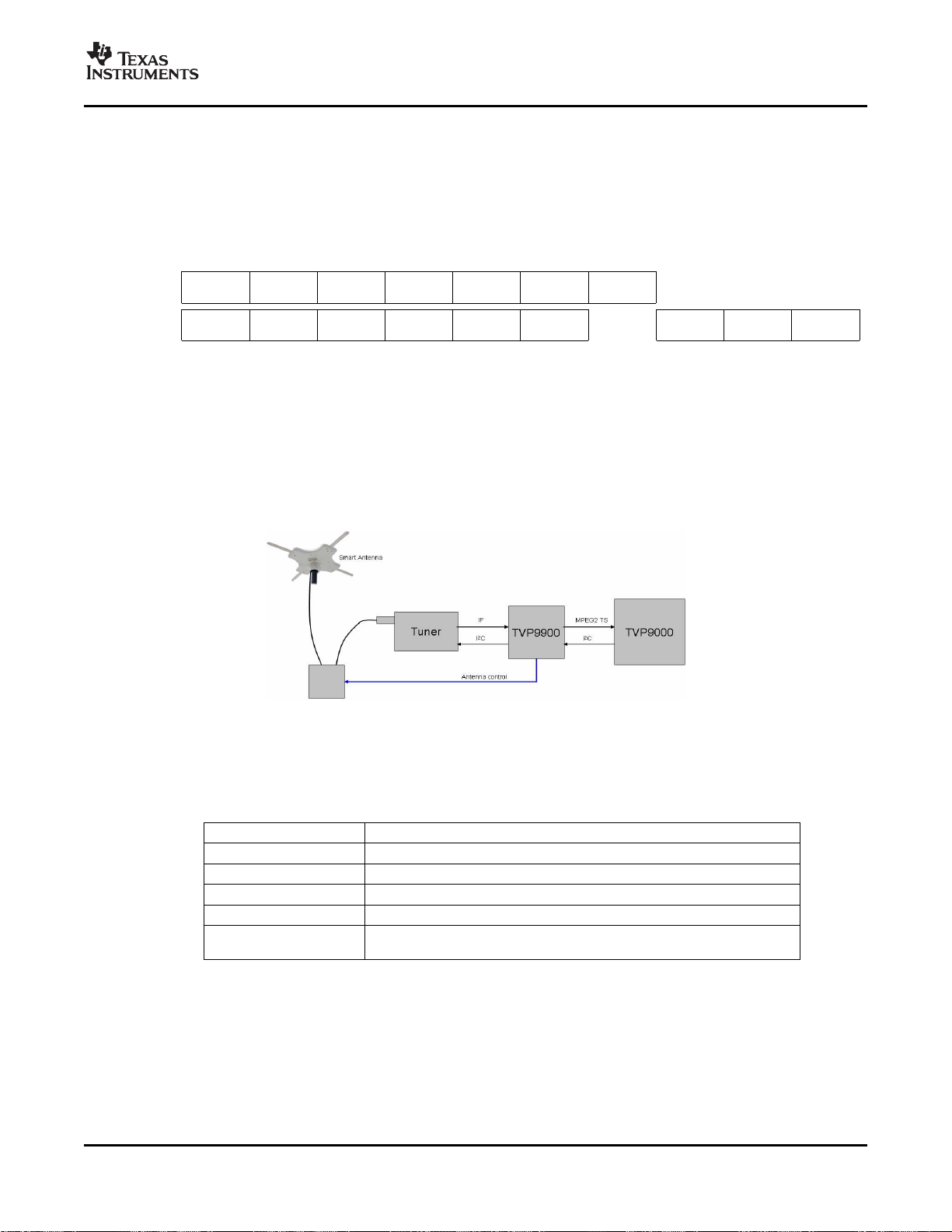
The TVP9900 has an antenna control interface compliant with EIA/CEA-909. The TVP9900 receives the
antenna parameters from the host processor via I2C, and sends a modulated PWM signal to the antenna.
The antenna parameters include antenna direction, antenna polarization, preamplifier gain and channel
number. This interface can be used to automatically optimize the signal by adjusting the antenna
configuration for the best possible reception.
Figure 4-6 shows the block diagram of the antenna control interface system.
Device Base
Address Address
Device
Address
Figure 4-6. Antenna Control Interface System
Table 4-7 lists the I2C registers and their functions used with the antenna control interface.
Table 4-7. Antenna Control Interface Registers
REGISTER FUNCTION
4Fh GPIO Alternate Function Select
5Fh Antenna Control Interface – Control and Status
60h to 61h Antenna Control Interface – Transmit Data
62h to 63h Antenna Control Interface – Receive Data
F9, FB, FD, FFh
Software Interrupt Raw Status, Status, Mask, and Clear – Transaction
Complete and Timeout Status
The TVP9900 supports two modes of antenna control: Mode A for basic control (transmit transaction only)
and Mode B for advanced control (transmit and receive transactions) as defined in the CEA-909 standard.
For Mode B operation, the TVP9900 supports both 1-pin and 2-pin operation. In 1-pin mode, the data
input and output are muxed into one pin (pin 29), and in 2-pin mode the input and output use separate
pins (pin 29 for output, pin 72 for input.) The desired pin mode is selected by setting register 5Fh, bit 0.
Submit Documentation Feedback Functional Description 19

www.ti.com
TVP9900
VSB/QAM Receiver
SLEA064 – MARCH 2007
Table 4-8 lists the TVP9900 pins and their functions used with the antenna control interface.
Table 4-8. Antenna Control Interface Pins
PIN NAME FUNCTION
29 ANTCNTLIO Antenna control interface input/output
71 GPIO1 Signal direction of pin 29 in 1-pin mode
72 GPIO0/ANTCNTLIN Antenna control input for 2-pin mode
The GPIO1 pin provides dedicated smart antenna control support, and in 1-pin mode this pin outputs the
direction of the signal on pin 29:
GPIO1 = 0 indicates signal input from antenna to TVP9900 pin 29
GPIO1 = 1 indicates signal output from TVP9900 pin 29 to antenna
Four status bit are provided in the TVP9900 to indicate the completion of a successful receive or transmit
transaction, or if a transaction timeout has occurred.
• The ACIRXCT bit in the TVP9900 Software Interrupt Status Register (FBh) gets set when the receive
transaction from a Mode B antenna is complete.
• The ACITXCT bit in the same register gets set when the transmit transaction to the antenna is
complete.
• The ACIRXTO bit in the same register gets set when an interface timeout has occurred due to no reply
form the antenna following a transmit transaction, or an incomplete receive transaction from the
antenna.
• The RXERR bit in the Antenna Control Interface Control and Status Register (5Fh) is set if an
incomplete receive transaction occurs.
The TVP9900 can be configured so that setting the ACIRXCT, ACITXCT, or ACIRXTO status bits can
assert the INTREQ output of the TVP9900; this requires the mask bits to be configured correctly in the
TVP9900 Software Interrupt Mask Register (FDh).
If the host INTREQ is not used, the ACIRXCT, ACITXCT, and ACIRXTO interrupts should be masked and
the host should poll the ACIRXCT and ACITXCT status bits to determine when the transactions are
complete, and the host should poll the ACIRXTO and RXERR status bits to determine when a receive
timeout or error has occurred.
Antenna control data transfers occur utilizing the following illustrated formats.
4.7.1 Antenna Interrogation/Initialization
The following steps are required to interrogate and initialize a smart antenna. The host processor first
writes the required transaction data to a set of registers in the TVP9900 via the host processor I2C
interface.
1. The system host processor transmits to the antenna a basic Mode A 14-bit serial data stream with an
RF channel number of zero.
2. The system tri-states the line and waits 100 ms for a reply message from the antenna controller. If no
response is received, a timeout occurs, and the antenna controller is assumed to be a Mode A system.
The system uses only transmit operations for antenna control.
3. If the antenna responds with a 10-bit program identifier, the antenna controller is assumed to be a
Mode B system, and the system uses transmit and receive operations for antenna control.
This initialization is optional. If the system has only Mode A enabled, with no Mode B support, then this
initialization step may be omitted.
Functional Description20 Submit Documentation Feedback
 Loading...