

现货库存、技术资料、百科信息、热点资讯,精彩尽在鼎好!
www.ti.com
TRIPLE 8/10-BIT, 165/110 MSPS, VIDEO
AND GRAPHICS DIGITIZER WITH ANALOG PLL
FEATURES APPLICATIONS
• Analog Channels
– -6 dB to 6 dB Analog Gain
– Analog Input MUXs
– Auto Video Clamp
– Three Digitizing Channels, Each With
Independently Controllable Clamp, PGA,
and ADC
– Clamping: Selectable Clamping Between
Bottom Level and Mid-level
– Offset: 1024-Step Programmable RGB or
YPbPr Offset Control
– PGA: 8-Bit Programmable Gain Amplifier
– ADC: 8/10-Bit 165/110 MSPS A/D Converter
– Automatic Level Control Circuit
– Composite Sync: Integrated Sync-on-Green
Extraction From GreenLuminance Channel
– Support for DC and AC-Coupled Input
Signals
• PLL
– Fully Integrated Analog PLL for Pixel Clock
Generation
– 12-165 MHz Pixel Clock Generation From
HSYNC Input
– Adjustable PLL Loop Bandwidth for
Minimum Jitter
– 5-Bit Programmable Subpixel Accurate
Positioning of Sampling Phase
• Output Formatter
– Support for RGB/YCbCr 4:4:4 and YCbCr TVP7001 also contains a complete analog PLL block
4:2:2 Output Modes to Reduce Board Traces
– Dedicated DATACLK Output for Easy
Latching of Output Data
• System
– Industry-Standard Normal/Fast I2C Interface
With Register Readback Capability
– Space-Saving TQFP-100 Pin Package
– Thermally-Enhanced PowerPAD™ Package
for Better Heat Dissipation
TVP7001
SLES164 – FEBBRUARY 2006
• LCD TV/Monitors/Projectors
• DLP TV/Projectors
• PDP TV/Monitors
• PCTV Set-Top Boxes
• Digital Image Processing
• Video Capture/Video Editing
• Scan Rate/Image Resolution Converters
• Video Conferencing
• Video/Graphics Digitizing Equipment
DESCRIPTION
TVP7001 is a complete solution for digitizing video
and graphic signals in RGB or YPbPr color spaces.
The device supports pixel rates up to 165 MHz.
Therefore, it can be used for PC graphics digitizing
up to the VESA standard of UXGA (1600 × 1200)
resolution at 60 Hz screen refresh rate, and in video
environments for the digitizing of digital TV formats,
including HDTV up to 1080p. TVP7001 can be used
to digitize CVBS and S-video signal with 10-bit ADCs.
The TVP7001 is powered from 3.3-V and 1.8-V
supply and integrates a triple high-performance A/D
converter with clamping functions and variable gain,
independently programmable for each channel. The
clamping timing window is provided by an external
pulse or can be generated internally. The TVP7001
includes analog slicing circuitry on the Y or G input to
support sync-on-luminance or sync-on-green
extraction. In addition, TVP7001 can extract discrete
HSYNC and VSYNC from composite sync using a
sync slicer.
to generate a pixel clock from the HSYNC input. Pixel
clock output frequencies range from 12 MHz to 165
MHz.
All programming of the part is done via an
industry-standard I2C interface, which supports both
reading and writing of register settings. The TVP7001
is available in a space-saving TQFP 100-pin
PowerPAD package.
Please be aware that an important notice concerning availability, standard warranty, and use in critical applications of Texas
Instruments semiconductor products and disclaimers thereto appears at the end of this data sheet.
PowerPAD is a trademark of Texas Instruments.
PRODUCTION DATA information is current as of publication date.
Products conform to specifications per the terms of the Texas
Instruments standard warranty. Production processing does not
necessarily include testing of all parameters.
Copyright © 2006, Texas Instruments Incorporated
www.ti.com
Output
Formatter
ROUT[9:0]
GOUT[9:0]
Host
Interface
Timing Processor
and Clock generation
RIN_1
SCL
SDA
I2CA
GIN_1
BIN_1
Clamp
Clamp
Clamp
PGA
PGA
PGA
10−bit
ADC
10−bit
ADC
10−bit
ADC
HSYNC_A
VSYNC_A
COAST
CLAMP
FILT1
SOGIN_1
RESETB
PWDN
BOUT[9:0]
SOGOUT
HSOUT
VSOUT
DATACLK
RIN_2
GIN_2
BIN_2
EXT_CLK
SOGIN_2
HSYNC_B
VSYNC_B
FILT2
RIN_3
GIN_3
GIN_4
SOGIN_3
BIN_3
TVP7001
SLES164 – FEBBRUARY 2006
T
A
0 ° C to 70 ° C
ORDERING INFORMATION
PACKAGED DEVICES
100-PIN PLASTIC FLATPACK PowerPAD™
TVP7001PZP Tray
TVP7001PZPR Reel
FUNCTIONAL BLOCK DIAGRAM
PACKAGE OPTION
2
Submit Documentation Feedback
www.ti.com
TVP7001
100−Pin TQFP Package
(Top View)
SOGIN_1
GIN_1
A18GND
A18VDD
A18GND
A18VDD
A18VDD
A18GND
RIN_3
RIN_2
RIN_1
A33GND
A33VDD
A33VDD
A33GND
BIN_3
BIN_2
BIN_1
A18VDD
A18GND
NSUB
TEST
VSOUT
HSOUT
SOGOUT
IOVDD
IOGND
B_9
B_8
B_7
B_6
B_5
B_4
B_3
B_2
B_1
B_0
DVDD
GND
IOVDD
IOGND
G_9
G_8
G_7
G_6
G_5
G_4
G_3
G_2
SDA
SCL
I2CA
TMS
RESETB
PWDN
DVDD
GND
IOGND
IOVDD
R_0
R_1
R_2
R_3
R_4
IOGND
R_5
R_6
R_7
R_8
R_9
IOGND
IOVDD
G_0
G_1
GIN_2
SOGIN_2
GIN_3
SOGIN_3
GIN_4
A33GND
A33VDD
A33VDD
A33GND
NSUB
PLL_A18GND
PLL_F
FILT2
FILT1
PLL_A18GND
PLL_A18VDD
PLL_A18VDD
PLL_A18GND
HSYNC_B
HSYNC_A
EXT_CLK
VSYNC_B
VSYNC_A
COAST
CLAMP
1
2
3
4
5
6
7
8
9
10
11
12
13
14
15
16
17
18
19
20
21
22
23
24
25
75
74
73
72
71
70
69
68
67
66
65
64
63
62
61
60
59
58
57
56
55
54
53
52
51
100
9998979695949392919089888786858483828180797877
76
26272829303132333435363738394041424344454647484950
TVP7001
SLES164 – FEBBRUARY 2006
TERMINAL ASSIGNMENTS
Submit Documentation Feedback
3
www.ti.com
TVP7001
SLES164 – FEBBRUARY 2006
TERMINAL FUNCTIONS
TERMINAL
NAME NO.
ANALOG VIDEO
RIN_1 11 I Analog video input for R/Pr 1
RIN_2 10 I Analog video input for R/Pr 2
RIN_3 9 I Analog video input for R/Pr 3
GIN_1 2 I Analog video input for G/Y 1
GIN_2 100 I Analog video input for G/Y 2
GIN_3 98 I Analog video input for G/Y 3
GIN_4 96 I Analog video input for G/Y 4
BIN_1 18 I Analog video input for B/Pb 1
BIN_2 17 I Analog video input for B/Pb 2
BIN_3 16 I Analog video input for B/Pb 3
CLOCK SIGNALS
DATACLK 28 O Data clock output
EXT_CLK 80 I External clock input for free running mode
TEST 22 O Internal 5 MHz clock output, coast output, high-Z, or SOG output
DIGITAL VIDEO
ROUT [9:0] 55–59, 61–65 O Digital video output of R/Cr, ROUT [9] is MSB.
GOUT [9:0] 43-52 O Digital video output of G/Y, GOUT [9] is MSB.
BOUT [9:0] 29-38 O Digital video output of B/Cb, BOUT [9] is MSB. For a 4:2:2 mode BOUT outputs CbCr data.
MISCELLANEOUS SIGNALS
PWDN 70 I Power down input. 1: Power down 0: Normal mode
RESETB 71 I Reset input, active low
TMS 72 I Connect to ground
FILT1 87 O External filter connection for PLL. The recommended capacitor is 0.1 µ F. see Figure 4
FILT2 88 O External filter connection for PLL. The recommended capacitor is 4.7 nF. See Figure 4
HOST INTERFACE
I2C A 73 I I2C Address input
SCL 74 I I2C Clock input
SDA 75 I/O I2C Data bus
POWER SUPPLIES
NSUB 21, 91 I Substrate ground. Connect to analog ground.
A33VDD 13, 14, 93, 94 I Analog power. Connect to 3.3 V.
A33GND 12, 15, 92, 95 I Analog 3.3 V return. Connect to Ground.
A18GND 3, 5, 8, 20 I Analog 1.8V return. Connect to Ground
A18VDD 4, 6, 7, 19 I Analog power. Connect to 1.8 V.
PLL_A18VDD 84, 85 I PLL analog power. Connect to 1.8 V.
PLL_F 89 I PLL filter internal supply connection
PLL_A18GND 83, 86, 90 I PLL analog power return. Connect to Ground.
GND 40, 68 I Digital return. Connect to Ground.
DVDD 39, 69 I Digital power. Connect to 1.8 V
IOGND I
IOVDD 26, 41, 53, 66 I Digital power. Connect to 3.3 V or less for reduced noise.
SYNC SIGNALS
CLAMP 76 I External Clamp input. Unused inputs can be connected to ground.
COAST 77 I External PLL COAST signal input. Unused inputs can be connected to ground
27, 42, 54, 60, Digital power return. Connect to Ground.
67
I/O DESCRIPTION
The inputs must be AC coupled. The recommended coupling capacitor is 0.1 µ F. Unused analog
inputs should be connected to ground using a 10 nF capacitor.
Unused outputs can be left unconnected.
4
Submit Documentation Feedback
www.ti.com
SLES164 – FEBBRUARY 2006
TERMINAL FUNCTIONS (continued)
TERMINAL
NAME NO.
VSYNC_A 78 I Vertical sync input A
VSYNC_B 79 I Vertical sync input B. Unused inputs can be connected to ground.
HSYNC_A 81 I Horizontal Sync input A
HSYNC_B 82 I Horizontal Sync input B. Unused inputs can be connected to ground.
SOGIN1 1 I Sync-on-green input 1
SOGIN2 99 I Sync-on-green input 2
SOGIN3 97 I Sync-on-green input 3. Unused inputs should be connected to ground using a 10 nF capacitor.
VSOUT 23 O Vertical sync output
HSOUT 24 O Horizontal sync output
SOGOUT 25 O Sync-on-green slicer output
I/O DESCRIPTION
ABSOLUTE MAXIMUM RATINGS
over operating free-air temperature range (unless otherwise noted)
IOVDD to IOGND –0.5 V to 4.5 V
Supply voltage range
Digital input voltage range VI to GND –0.5 V to 4.5 V
Analog input voltage range AI to A33GND –0.2 V to 2.3 V
Digital output voltage range VO to GND –0.5 V to 4.5 V
TA Operating free-air temperature 0 ° C to 70 ° C
Tstg Storage temperature –65 ° C to 150 ° C
(1) Stresses beyond those listed under absolute maximum ratings may cause permanent damage to the device. These are stress ratings
only and functional operation of the device at these or any other conditions beyond those indicated under recommended operating
conditions is not implied. Exposure to absolute–maximum–rated conditions for extended periods may affect device reliability.
DVDD to GND –0.5 V to 2.3 V
PLL_A18VDD to PLL_A18GND and A18VDD to A18GND –0.5 V to 2.3 V
A33VDD to A33GND – 0.5 V to 4.5 V
(1)
UNIT
TVP7001
RECOMMENDED OPERATING CONDITIONS
over operating free-air temperature range, TA= 0 ° C to 70 ° C (unless otherwise noted)
MIN NOM MAX UNIT
IOVDD Digital I/O supply voltage 3.0 3.3 3.6 V
DVDD Digital supply voltage 1.70 1.8 2.0 V
PLL_A18VDD Analog PLL supply voltage 1.8 1.9 2.0 V
A18VDD Analog supply voltage 1.8 1.9 2.0 V
A33VDD Analog supply voltage 3.0 3.3 3.6 V
V
I(P–P)
V
IH
V
IL
I
OH
I
OL
I
OH_DATACLK
I
OL_DATACLK
T
A
Analog input voltage (ac–coupling necessary) 0.5 2.0 V
Digital input voltage high 0.7 IOVDD V
Digital input voltage low 0.3 IOVDD V
High–level output current 2 mA
Low–level output current –2 mA
DATACLK high–level output current 4 mA
DATACLK low–level output current –4 mA
Operating free–air temperature 0 70 ° C
Submit Documentation Feedback
5

www.ti.com
TVP7001
SLES164 – FEBBRUARY 2006
ELECTRICAL CHARACTERISTICS
IOVDD = 3.3 V, DVDD = 1.8 V, PLL_A18VDD = 1.9 V, A18VDD = 1.9 V, A33VDD = 3.3 V, TA= 25 ° C
PARAMETER TEST CONDITIONS MIN TYP
POWER SUPPLY
I
A33VDD
I
IOVDD
I
A18VDD
I
PLL_18VDD
I
DVDD
P
TOT
I
A33VDD
I
IOVDD
I
A18VDD
I
PLL_18VDD
I
DVDD
P
TOT
P
DOWN
(1) SMPTE color bar RGB input pattern used.
(2) Worst case vertical line RGB input pattern used.
3.3-V supply current 78.75 MHz 60 60 mA
3.3-V supply current 78.75 MHz 32 78 mA
1.8-V supply current 78.75 MHz 225 225 mA
1.8-V supply current 78.75 MHz 14 14 mA
1.8-V supply current 78.75 MHz 7 9 mA
Total power dissipation, normal mode 78.75 MHz 746 901 mW
3.3-V supply current 162 MHz 95 95 mA
3.3-V supply current 162 MHz 44 125 mA
1.8-V supply current 162 MHz 230 230 mA
1.8-V supply current 162 MHz 20 20 mA
1.8-V supply current 162 MHz 17 20 mA
Total power dissipation, normal mode 162 MHz 936 1200 mW
Total power dissipation, power–down mode 1 mW
(1)
(2)
MAX
UNIT
6
Submit Documentation Feedback
www.ti.com
TVP7001
SLES164 – FEBBRUARY 2006
ELECTRICAL CHARACTERISTICS
IOVDD = 3.3 V, DVDD = 1.8 V ± 0.1, PLL_A18VDD = 1.9 V ± 0.1, A18VDD = 1.9 V ± 0.1, A33VDD = 3.3 V, TA= 0 ° C to 70 ° C
(unless otherwise noted)
PARAMETER TEST CONDITIONS MIN TYP MAX UNIT
ANALOG INTERFACE
Input voltage range By design 0.5 1.0 2.0 Vpp
Z
I
DIGITAL LOGIC INTERFACE
C
I
Z
I
V
OH
V
OL
V
OH_SCLK
V
OL_SCLK
V
IH
V
IL
A/D CONVERTERS
DNL DC differential nonlinearity LSB
INL DC integral nonlinearity LSB
SNR Signal-to-noise ratio 10 MHz, 1.0 V
PLL
Input impedance, analog video inputs By design 500 k Ω
Input capacitance By design 10 pF
Input impedance By design 500 k Ω
Output voltage high IOH= 2 mA 0.8 IOVDD V
Output voltage low IOL= –2 mA 0.2 IOVDD V
DATACLK output voltage high IOH= 4 mA 0.8 IOVDD V
DATACLK output voltage low IOH= –2 mA 0.2 IOVDD V
High-level input voltage By design 0.7 IOVDD V
Low-level input voltage By design 0.3 IOVDD V
Conversion rate 12 165 MSPS
10 bit, 110 MHz -1 ± 0.5 +1
8 bit, 162 MHz -1 ± 0.5 +1
10 bit, 110 MHz -4 ± 1 +4
8 bit, 162 MHz -4 ± 1 +4
Missing code 8 bit, 162 MHz none
at 110 52 dB
MSPS
P–P
Analog bandwidth By design 500 MHz
Clock jitter 500 ps
Phase adjustment 11.6 degree
VCO frequency range 12 165 MHz
Submit Documentation Feedback
7
www.ti.com
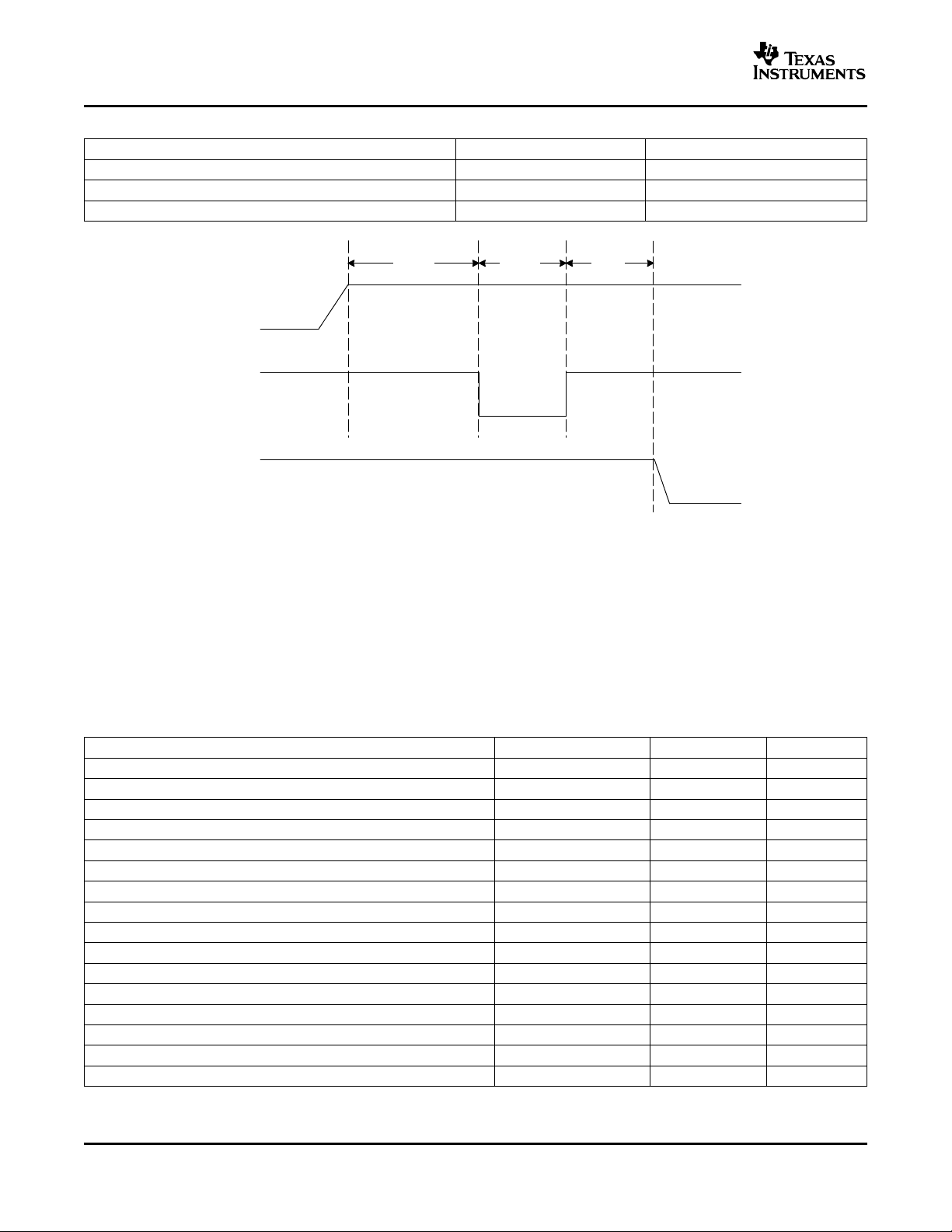
DATACLK
t1
t2
t3
Valid DataR, G, B, HSOUT Valid Data
TVP7001
SLES164 – FEBBRUARY 2006
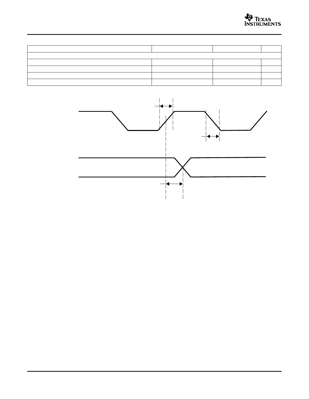
TIMING REQUIREMENTS
PARAMETER TEST CONDITIONS
CLOCKS, VIDEO DATA, SYNC TIMING
Duty cycle DATACLK 50%
t
t
t
(1) Measured with a load of 15 pF.
DATACLK rise time 10% to 90% 1 ns
1
DATACLK fall time 90% to 10% 1 ns
2
Output delay time 1.5 3.5 ns
3
(1)
MIN TYP MAX UNIT
Figure 1. Clock, Video Data, and Sync Timing
8
Submit Documentation Feedback
www.ti.com
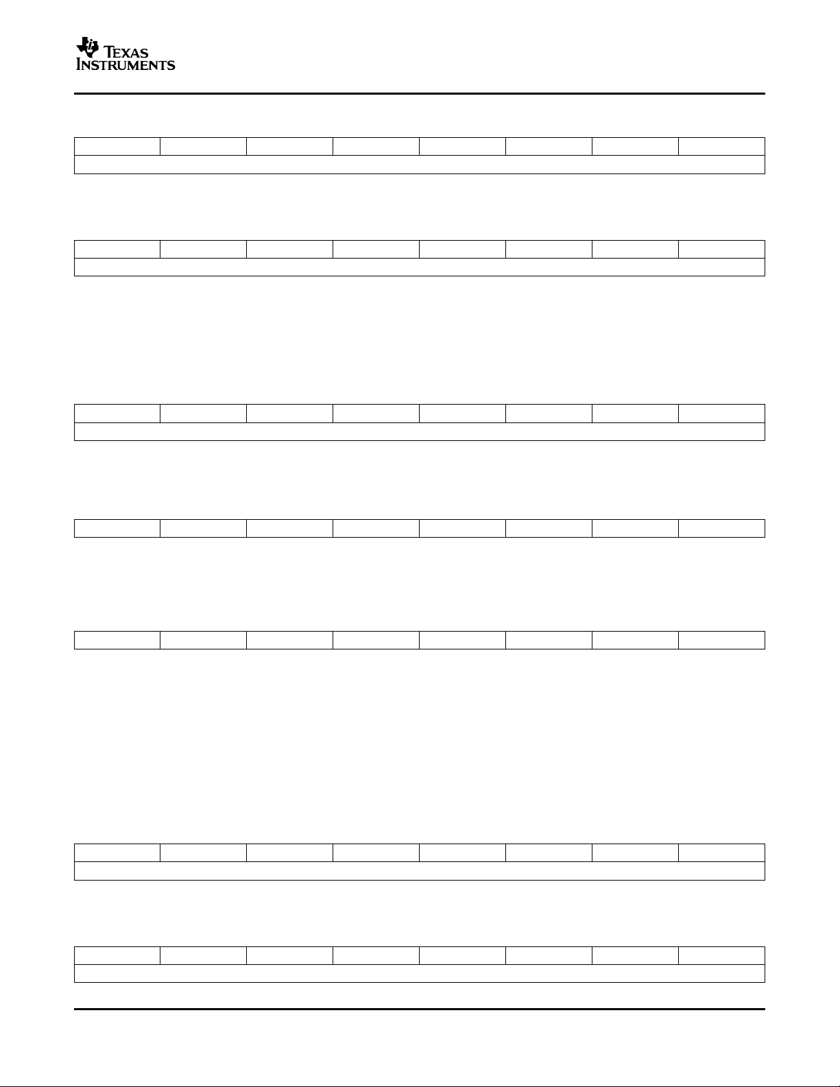
TIMING REQUIREMENTS
SDA
t1
t6
t7
t2
t8
t3
t4
t6
SCL
Data
Stop Start Stop
t5
I2C HOST PORT TIMING
t
1
t
2
t
3
t
4
t
5
t
6
t
7
t
8
C
b
f
12C
TVP7001
SLES164 – FEBBRUARY 2006
PARAMETER TEST CONDITIONS MIN TYP MAX UNIT
Bus free time between STOP and START Specified by design 1.3 µ s
Setup time for a (repeated) START condition Specified by design 0.6 µ s
Hold time (repeated) START condition Specified by design 0.6 µ s
Setup time for a STOP condition Specified by design 0.6 ns
Data setup time Specified by design 100 ns
Data hold time Specified by design 0 0.9 µ s
Rise time SDA and SCL signal Specified by design 250 ns
Fall time SDA and SCL signal Specified by design 250 ns
Capacitive load for each bus line Specified by design 400 pF
I2C clock frequency Specified by design 400 kHz
Figure 2. I2C Host Port Timing
Submit Documentation Feedback
9

www.ti.com
TVP7001
SLES164 – FEBBRUARY 2006
FUNCTIONAL DESCRIPTION
Analog Channel
The TVP7001 contains three identical analog channels that are independently programmable. Each channel
consists of a clamping circuit, a programmable gain amplifier, automatic offset control and an A/D converter.
Analog Input Switch Control
TVP7001 has 3 analog channels that accept up to 10 video inputs. The user can configure the internal analog
video switches via the I2C interface. The 10 analog video inputs can be used for different input configurations
some of which are:
• Up to 10 selectable individual composite video inputs
• Up to 2 selectable RGB graphics inputs
• Up to 3 selectable YPbPr video HD/SD inputs
The input selection is performed by the input select register at I2C subaddress 0 × 19 and 0 × 1A (see Input Mux
Select 1 and Input Mux Select 2)
Analog Input Clamping
An internal clamping circuit restores the AC-coupled video/graphic signal to a fixed DC level. The clamping circuit
provides line-by-line restoration of the signal black level to a fixed DC reference voltage. The selection between
bottom and mid level clamping is performed by I2C subaddress 0 × 10 (see Sync On_Green Threshold). Fine
clamps must also be enabled in the I2C register 2Ah for proper operation.
The internal clamping time can be adjusted by I2C clamp start and width registers at subaddress 0 × 05 and 0 × 06
(see Clamp Start and Clamp Width).
Programmable Gain Amplifier (PGA)
The TVP7001 PGA can scale a signal with a voltage-input compliance of 0.5-Vpp to 2-Vpp to a full-scale 10-bit
A/D output code range. A 4-bit code sets the coarse gain (Red Coarse Gain, Green Coarse Gain, Blue Coarse
Gain) with individual adjustment per channel. Minimum gain corresponds to a code 0 × 0 (2-Vpp full-scale input,
–6 dB gain) while maximum gain corresponds to code 0 × F (0.5-Vpp full-scale, +6 dB gain). TVP7001 also has
8-bit fine gain control (Red Fine Gain, Green Fine Gain, Blue Fine Gain) for RGB independently ranging from 1
to 2. For a normal PC graphics input, the fine gain will be used mostly.
Programmable Offset Control and Automatic Level Control (ALC)
The TVP7001 supports a programmable offset control for RGB independently. A 6-bit code sets the coarse offset
(Red Coarse Offset, Green Coarse Offset, Blue Coarse Offset) with individual adjustment per channel. The
coarse offset ranges from –32 LSB to +31 LSB. The coarse offset registers apply before the ADC. A 10-bit fine
offset registers (Red Fine Offset, Green Fine Offset, Blue Fine Offset) apply after the ADC. The fine offset ranges
from –512 LSB to +511 LSB.
ALC circuit maintains the level of the signal to be set at a value which is programmed at fine offset I2C register. It
consists of pixel averaging filter and feedback loop. This ALC function can be enabled or disabled by I2C register
address at 0 × 26. ALC circuit needs a timing pulse generated internally but user should program the position
properly. The ALC pulse must be positioning after the clamp pulse. The position of ALC pulse is controlled by
ALC placement I2C register at address 0 × 31. This is available only for internal ALC pulse timing. For external
clamp, the timing control of clamp is not applicable so the ALC pulse control is also not applicable. Therefore it is
suggested to keep the external clamp pulse as long as possible. ALC is applied as same position of external
clamp pulse.
A/D Converters
All ADCs have a resolution of 10-bits and can operate up to 165 MSPS. All A/D channels receive an identical
clock from the on-chip phase-locked loop (PLL) at a frequency between 12 MHz and 165 MHz. All ADC
reference voltages are generated internally. Also the external sampling clock can be used.
10
Submit Documentation Feedback

www.ti.com
COAST
HSYNC
Phase
Detector
PLL Control
Register 0x03
Bit [5:3]
PLL Control
Register 0x03
Bit [7:6]
Phase Select
Register 0x04
Bit [7:3]
Charge
Pump
VCO
Phase
Select
Divider
ADC
Sampling
CLK
External
Clock
PLL Divide
Register 0x01
and 0x02
Bit [11:0]
Loop
Filter
÷ N
N = 1 or 2
TVP7001
SLES164 – FEBBRUARY 2006
Analog PLL
The analog PLL generates a high-frequency internal clock used by the ADC sampling and data clocking out to
derive the pixel output frequency with programmable phase. The reference signal for this PLL is the horizontal
sync signal supplied on the HSYNC input or from extracted horizontal sync of sync slicer block for embedded
sync signals. The analog PLL consisted of phase detector, loop filter, voltage controlled oscillator (VCO), divider
and phase select. The analog block diagram is shown at Figure 3 .
Figure 3. PLL Block Diagram
The COAST signal is used to allow the PLL to keep running at the same frequency, in the absence of the
incoming HSYNC signal or disordered HSYNC period. This is useful during the vertical sync period, or any other
time that the HSYNC is not available.
There are several PLL controls to produce the correct sampling clock. The 12-bit divider register is
programmable to select exact multiplication number to generate the pixel clock in the range of 12 MHz to 165
MHz. The 3-bit loop filter current control register is to control the charge pump current that drives the low-pass
loop filter. The applicable current values are listed in the Table 1 .
The 2-bit VCO range control is to improve the noise performance of the TVP7001. The frequency ranges for the
VCO are shown in Table 1 . The phase of the PLL generated clock can be programmed in 32 uniform steps over
a single clock period (360/32=11.25 degrees phase resolution) so that the sampling phase of the ADC can be
accurately controlled.
In addition to sourcing the ADC channel clock from the PLL, an external pixel clock can be used (from pin 80).
The PLL characteristics are determined by the loop filter design, by the PLL charge pump current, and by the
VCO range setting. The loop filter design is shown in Figure 4 . Supported settings of VCO range and charge
pump current for VESA standard display modes are listed in Table 1 .
Submit Documentation Feedback
11

www.ti.com
0.1 µF
4.7 nF
1.5 kΩ
TVP7000
PLL_F
FILT2
FILT1
89
88
87
TVP7001
SLES164 – FEBBRUARY 2006
Figure 4. PLL Loop Filter
Table 1. Recommended VCO Range and Charge Pump Current Settings for Supporting Standard Display
Formats
STANDAR RESOL. REFRESH HORIZ. PIXEL PLL Divider PLLDIV [11:4] PLLDIV [3:0] Reg 03h Output VCO CP CURRENT
D RATE FREQ. (kHz) RATE Total Reg 01h [7:0] Reg 02h [7:4] Divider Reg RANGE Reg Reg 03h [5:3]
VGA 640 × 480 60 Hz 31.5 25.175 1600(2 × ) 64h 00h 68h 1 Low (01b) 101b
72 Hz 37.9 31.5 1664(2 × ) 68h 00h 58h 1 Low (01b) 011b
75 Hz 37.5 31.5 1680(2 × ) 69h 00h 58h 1 Low (01b) 011b
85 Hz 43.3 36 832 34h 00h 68h 0 Low (01b) 101b
SVGA 800 × 600 56 Hz 35.1 36 1024 40h 00h 68h 0 Low (01b) 101b
60 Hz 37.9 40 1056 42h 00h 68h 0 Low (01b) 101b
72 Hz 48.1 50 1040 41h 00h 68h 0 Low (01b) 101b
75 Hz 46.9 49.5 1056 42h 00h 68h 0 Low (01b) 101b
85 Hz 53.7 56.25 1048 41h 80h 68h 0 Low (01b) 101b
XGA 1024 × 768 60 Hz 48.4 65 1344 54h 00h 58h 0 Low (01b) 011b
70 Hz 56.5 75 1328 53h 00h A8h 0 Med (10b) 101b
75 Hz 60 78.75 1312 52h 00h A8h 0 Med (10b) 101b
85 Hz 68.7 94.5 1376 56h 00h A8h 0 Med (10b) 101b
SXGA 1280 × 1024 60 Hz 64 108 1688 69h 80h A8h 0 Med (10b) 101b
75 Hz 80 135 1688 69h 80h 98h 0 Med (10b) 011b
UXGA 1600 × 1200 60 Hz 75 162 2160 87h 00h F8h 0 High (11b) 011b
Video 720 × 480p 60 Hz 31.468 27 1716(2 × ) 6Bh 40h 68h 1 Low (01b) 101b
720 × 576p 50 Hz 31.25 27 1728(2 × ) 6Ch 00h 68h 1 Low (01b) 101b
1280 × 720p 60 Hz 45 74.25 1650 67h 20h A8h 0 Med (10b) 101b
1280 × 720p 50 Hz 37.5 74.25 1980 7Bh C0h A8h 0 Med (10b) 101b
1920 × 1080i 60 Hz 33.75 74.25 2200 89h 80h A8h 0 Med (10b) 101b
1920 × 1080i 50 Hz 28.125 74.25 2640 A5h 00h A8h 0 Med (10b) 101b
1920 × 1080p 60 Hz 67.5 148.5 2200 89h 80h D8h 0 High (11b) 011b
1920 × 1080p 50 Hz 56.25 148.5 2640 A5h 00h D8h 0 High (11b) 011b
(MHz) pix/line 04h [0] 03h [7:6]
Sync Slicer
TVP7001 includes a circuit that compares the input signal on Green channel to a level 150mV (typical value)
above the clamped level (sync tip). The slicing level is programmable by I2C register subaddress at 0x10. The
digital output of the composite sync slicer is available on the SOGOUT pin.
Sync Separator
The sync separator automatically extracts VSYNC and HSYNC from the sliced composite sync input supplied at
the SOG input. The G or Y input containing the composite sync must be AC coupled to the SOG input pin using
a 10-nF capacitor. Support for PC graphics, SDTV, and HDTV up to 1080p is provided.
12
Submit Documentation Feedback

www.ti.com
Clock
Generation
SYNC
Slicer
SYNC
Separator
5MHz
CLK
Polarity
Detect
SOG
Phase
Select
ADCDIV
HSYNC
VSYNC
COAST
Activity
Detect
Activity
Detect
DATACLK
SOGOUT
VSOUT
COAST
HSYNC
Activity
Detect
HSOUT
TVP7001
SLES164 – FEBBRUARY 2006
Figure 5. Sync Processing
Timing
The TVP7001 supports RGB/YCbCr 4:4:4 and YCbCr 4:2:2 modes. Output timing is shown in Figure 6 . All timing
diagrams are shown for operation with internal PLL clock at phase 0. For a 4:2:2 mode, CbCr data outputs at
BOUT[9:0] pins.
Submit Documentation Feedback
13

www.ti.com
RGBin
HSYNC
DATACLK
RGBout
HSOUT
RGBin
HSYNC
DATACLK
HSOUT
GOUT
BOUT
P0 P1 P3 P10 P11 P12
13 clocks latency
D0 D1 D3 D4 D5
Programmable Width
P0 P1 P3 P10 P11 P12
13 clocks latency
Programmable Width
Y0 Y1 Y2 Y3 Y4
Cb2 Cr2 Cb4Cb0 Cr0
4:4:4: RGB/YCbCr Output Timing
4:2:2 YCbCr Output Timing
TVP7001
SLES164 – FEBBRUARY 2006
14
Figure 6. Output Timing Diagram
Submit Documentation Feedback

www.ti.com
TVP7001
SLES164 – FEBBRUARY 2006
I2C Host Interface
Communication with the TVP7001 device is via an I2C host interface. The I2C standard consists of two signals,
serial input/output data (SDA) line and input clock line (SCL), which carry information between the devices
connected to the bus. A third signal (I2CA) is used for slave address selection. Although an I2C system can be
multi-mastered, the TVP7001 can function as a slave device only.
Since SDA and SCL are kept open-drain at logic high output level or when the bus is not driven, the user should
connect SDA and SCL to a positive supply voltage via a pull up resistor on the board. SDA is implemented
bi-directional. The slave addresses select, terminal 73 (I2CA), enables the use of two TVP7001 devices tied to
the same I2C bus since it controls the least significant bit of the I2C device address
Table 2. I2C Host Interface Terminal Description
SIGNAL TYPE DESCRIPTION
I2C A I Slave address selection
SCL I Input clock line
SDA I/O Input/output data line
Reset and I2C Bus Address Selection
TVP7001 can respond to two possible chip addresses. The address selection is made at reset by an externally
supplied level on the I2C A pin. The TVP7001 device samples the level of terminal 73 at power- up or at the
trailing edge of RESETB and configures the I2C bus address bit A0. The I2C A terminal has an internal pull-down
resistor to pull the terminal low to set a zero.
Table 3. I2C Host Interface Device Addresses
A6 A5 A4 A3 A2 A1 A0 (I2C A) R/W HEX
1 0 1 1 1 0 0 (default) 1/0 B9/B8
1 0 1 1 1 0 1
(1) If terminal 73 strapped to DVDD via a 2.2 k Ω resistor, I2C device address A0 is set to 1.
(1)
1/0 BB/BA
I2C Operation
Data transfers occur utilizing the following illustrated formats.
S 10111000 ACK subaddress ACK send data ACK P
Read from I2C control registers
S 10111000 ACK subaddress ACK S 10111001 ACK receive data NAK P
S = I2C Bus Start condition
P = I2C Bus Stop condition
ACK = Acknowledge generated by the slave
NAK = Acknowledge generated by the master, for multiple byte read master with ACK each byte except last byte
Subaddress = Subaddress byte
Data = Data byte, if more than one byte of DATA is transmitted (read and write), the subaddress pointer is automatically
I2C bus address = Example shown that I2C A is in default mode. Write (B8h), Read (B9h)
incremented
Power-up, Reset, and Initialization
No specific power-up sequence is required, but all power supplies should be active and stable within 500 ms of
each other. Reset may be low during power-up, but must remain low for at least 1 µ s after the power supplies
become stable. Alternately reset may be asserted any time with minimum 5 ms delay after power-up and must
remain asserted for at least 1 µ s. Reset timing is shown in Figure 7 . It is also recommended that any I2C
operation starts 1 µ s after reset ended. Table 4 describes the status of the TVP7001 terminals during and
immediately after reset.
Submit Documentation Feedback
15
www.ti.com
Power
Reset
I2C
5 ms 1 µs 1 µs
TVP7001
SLES164 – FEBBRUARY 2006
Table 4. Reset Sequence
SIGNAL NAME DURING RESET RESET COMPLETED
ROUT[9:0], BOUT[9:0], BOUT[9:0] High impedance Output
HSOUT, VSOUT, SOGOUT High impedance Output
DATACLK High impedance Output
Figure 7. Reset Timing
Control Registers
The TVP7001 is initialized and controlled by a set of internal registers that define the operating parameters of the
entire device. Communication between the external controller and the TVP7001 is through a standard I2C host
port interface, as described earlier.
Table 5 shows the summary of these registers. Detailed programming information for each register is described
in the following sections.
Table 5. Control Registers Summary
Register Name I2C Subaddress Default R/W
Chip Revision 00h 00h R
PLL Divide MSB 01h 69h R/W
PLL Divide LSB 02h D0h R/W
PLL Control 03h 48h R/W
Phase Select 04h 80h R/W
Clamp Start 05h 80h R/W
Clamp Width 06h 80h R/W
HSYNC Output Width 07h 20h R/W
Blue Fine Gain 08h 80h R/W
Green Fine Gain 09h 80h R/W
Red Fine Gain 0Ah 80h R/W
Blue Fine Offset 0Bh 80h R/W
Green Fine Offset 0Ch 80h R/W
Red Fine Offset 0Dh 80h R/W
Sync Control 1 0Eh 40h R/W
PLL and Clamp Control 0Fh 4Eh R/W
(1) Register addresses not shown in the register map summary are reserved and must not be written to.
(2) Writing to or reading from any value labeled “Reserved” register may cause erroneous operation of the TVP7001. For registers with
reserved bits, a 0b must be written to reserved bit locations unless otherwise stated.
(1) (2)
16
Submit Documentation Feedback

www.ti.com
SLES164 – FEBBRUARY 2006
Table 5. Control Registers Summary (continued)
Register Name I2C Subaddress Default R/W
Sync On Green Threshold 10h B8h R/W
Sync Separator Threshold 11h 20h R/W
Pre-Coast 12h 00h R/W
Post-Coast 13h 00h R/W
Sync Detect Status 14h R
Output Formatter 15h 00h R/W
Test Register 16h 00h R/W
Reserved 17h–18h
Input Mux Select 1 19h 00h R/W
Input Mux Select 2 1Ah 00h R/W
Blue and Green Coarse Gain 1Bh 55h R/W
Red Coarse Gain 1Ch 05h R/W
Fine Offset LSB 1Dh 00h R/W
Blue Coarse Offset 1Eh 20h R/W
Green Coarse Offset 1Fh 20h R/W
Red Coarse Offset 20h 20h R/W
HSOUT Output Start 21h 09h R/W
MISC Control 22h 00h R/W
Reserved 23h–25h
Automatic Level Control Enable 26h 00h R/W
Reserved 27h
Automatic Level Control Filter 28h 00h R/W
Reserved 29h
Fine Clamp Control 2Ah 00h R/W
Power Control 2Bh 00h R/W
ADC Setup 2Ch 00h R/W
Coarse Clamp Control 1 2Dh 00h R/W
SOG Clamp 2Eh 00h R/W
Reserved 2Fh–30h
ALC Placement 31h 00h R/W
R = Read only
W = Write only
R/W = Read Write
TVP7001
Register Definitions
Chip Revision
Subaddress 00h Read Only
7 6 5 4 3 2 1 0
Chip revision [7:0]
Chip revision [7:0]: Chip revision number
Submit Documentation Feedback
17

www.ti.com
TVP7001
SLES164 – FEBBRUARY 2006
PLL Divide
Subaddress 01h–02h Default (69D0h)
7 6 5 4 3 2 1 0
PLL divide MSB [11:4]
PLL divide LSB [3:0] Reserved
PLL divide [11:0]: PLL divide number sets the number of pixels per line. Controls the PLL feedback divider. MSB [11:4] bits should be loaded
first whenever a change is required
PLL Control
Subaddress 03h Default (48h)
7 6 5 4 3 2 1 0
VCO[1:0] Charge Pump Current [2:0] Reserved Reserved Reserved
VCO [1:0]: Selects VCO frequency range
00 = Ultra low, less than 20 MHz
01 = Low (default), 20 MHz to 69 MHz
10 = Medium, 70 MHz to 135 MHz
11 = High, 136 MHz to 165 MHz
Charge Pump Current [2:0]: Selects charge current of PLL LPF
000 = Small (default)
111 = Large
Phase Select
Subaddress 04h Default (80h)
7 6 5 4 3 2 1 0
Phase Select [4:0] Reserved DIV2
Phase Select [4:0]: ADC Sampling clock phase select. (1 LSB = 360/32 = 11.25 ° )
DATACLK Divide-by-2
0 = DATACLK/1
1 = DATACLK/2
Clamp Start
Subaddress 05h Default (80h)
7 6 5 4 3 2 1 0
Clamp Start [7:0]
Clamp Start [7:0]: Positions the clamp signal an integer number of clock periods after the HSYNC signal. If external clamping is selected this
value has no meaning. Clamp Start must be correctly positioned for proper operation. See Table 6 for the recommended settings.
Clamp Width
Subaddress 06h Default (80h)
7 6 5 4 3 2 1 0
Clamp Width [7:0]
Clamp Width [7:0]: Sets the width in pixels for clamp. See register Clamp Start.
Table 6. Recommended Fine Clamp Settings
VIDEO STANDARD CLAMP START CLAMP WIDTH
HDTV (tri-level) 50 (32h) 32 (20h)
SDTV (bi-level) 6 (06h) 16 (10h)
PC Graphics 6 (06h) 16 (10h)
18
Submit Documentation Feedback
www.ti.com
SLES164 – FEBBRUARY 2006
HSYNC Output Width
Subaddress 07h Default (20h)
7 6 5 4 3 2 1 0
HSOUT Width [7:0]
HSOUT Width [7:0]: Sets the width in pixels for HSYNC output.
Blue Fine Gain
Subaddress 08h Default (80h)
7 6 5 4 3 2 1 0
Blue Gain [7:0]
Blue Gain [7:0]: PGA digital gain (contrast) for Blue channel applied after the ADC. Fine Gain = 1 + Blue Gain[7:0]/256
Blue Fine Gain Fine Gain
00h 1.0
80h 1.5 (default)
FFh 2.0
Green Fine Gain
Subaddress 09h Default (80h)
7 6 5 4 3 2 1 0
Green Gain [7:0]
Green Gain [7:0]: PGA digital gain (contrast) for Green channel applied after the ADC. Fine Gain = 1 + Green Gain[7:0]/256
80h = 1.5 (default)
TVP7001
Red Fine Gain
Subaddress 0Ah Default (80h)
7 6 5 4 3 2 1 0
Red Gain [7:0]
Red Gain [7:0]: Sets PGA digital gain (contrast) for Red channel applied after the ADC. Fine Gain = 1 + Red Gain[7:0]/256
80h = 1.5 (default).
Blue Fine Offset
Subaddress 0Bh Default (80h)
7 6 5 4 3 2 1 0
Blue Offset [9:2]
Blue Offset [9:2]: DC digital offset (brightness) for Blue channel applied after the ADC.
The default setting of 80h will place the bottom-level (YRGB) clamped output blank levels at 0 and mid-level clamped (PbPr) output blank
levels at 512.
Blue Offset Description
11111111 maximum
100000001 1 LSB
10000000 0 (default)
01111111 –1 LSB
00000000 minimum
Green Fine Offset
Subaddress 0Ch Default (80h)
7 6 5 4 3 2 1 0
Green Offset [9:2]
Green Offset [9:2]: DC digital offset (brightness) for Green channel applied after the ADC. See Red Fine Offset register at I2C address 0x0B
Red Fine Offset
Subaddress 0Dh Default (80h)
7 6 5 4 3 2 1 0
Red Offset [9:2]
Red Offset [9:2]: DC digital offset (brightness) for Red channel applied after the ADC. See Blue Fine Offset register at I2C address 0x0B.
Submit Documentation Feedback
19
www.ti.com
TVP7001
SLES164 – FEBBRUARY 2006
Sync Control 1
Subaddress 0Eh Default (40h)
7 6 5 4 3 2 1 0
HSPO HSIP HSOP AHSO AHSS VSOI AVSO AVS
HSPO: HSYNC Polarity Override
0 = Polarity determined by chip (default)
1 = Polarity set by Bit 6 in register 0Eh
HSIP: HSYNC Input Polarity
0 = Indicates input HSYNC polarity active low
1 = Indicates input HSYNC polarity active high (default)
HSOP: HSYNC Output Polarity
0 = Active low (default)
1 = Active high
AHSO: Active HSYNC Override
0 = The active interface is selected via Bit 6 in register 14h, selected by chip (default)
1 = The user can select HSYNC to be used via Bit 3
AHSS: Active HSYNC Select. The indicated HSYNC will be used only if Bit 4 is set to 1 or both syncs are active (Bits 1,7 =1 in 14h)
0 = Select HSYNC as the active sync (default)
1 = Select Sync-on-green as the active sync
VSOI: VSYNC Output Invert (relative to VSYNC IN polarity)
0 = No invert (default)
1 = Invert
AVSO: Active VSYNC Override
0 = The active interface is selected via Bit3 in register 14h, selected by chip (default)
1 = The user can select the VSYNC to be used via Bit 0
AVS: Active VSYNC select, This bit is effective when AVSO Bit 1 is set to 1.
0 = Raw VSYNC (default)
1 = Sync separated VSYNC
PLL and Clamp Control
Subaddress 0Fh Default (4Eh)
7 6 5 4 3 2 1 0
CF CP Coast Sel CPO CPC Reserved FCPD Free run
Clamp Function:
0 = Internal Clamp(default)
1 = External Clamp
Clamp Polarity:
0 = Active high
1 = Active low (default)
Coast Select:
0 = External coast (default)
1 = Internal Coast
Coast Polarity Override:
0 = Polarity determined by chip (default)
1 = Polarity set be Bit 3 in register 0Fh
Coast Polarity Change:
0 = Active low
1 = Active high (default)
Full Chip Power-Down:
0 = Power-down mode
1 = Normal operation (default)
Free run: Also ADC test mode, ADC uses external clock
0 = PLL normal operation (default)
1 = Enabled
20
Submit Documentation Feedback
www.ti.com
TVP7001
SLES164 – FEBBRUARY 2006
Sync On_Green Threshold
Subaddress 10h Default (B8h)
7 6 5 4 3 2 1 0
SOG Threshold [4:0] Blue CS Green CS Red CS
SOG Threshold [4:0]: Sets the voltage level of the SOG slicer comparator. The minimum setting is 0 mV and the maximum is 350 mV. The
step is 11.2 mV. (default 17h, 10h recommended)
Blue Clamp Select: When free running mode this bit is no effect
0 = Bottom level clamp (default)
1 = Mid level clamp
Green Clamp Select: When free running mode this bit is no effect
0 = Bottom level clamp (default)
1 = Mid level clamp
Red Clamp Select: When free running mode this bit is no effect.
0 = Bottom level clamp (default)
1 = Mid level clamp
NOTE:
Bottom level clamping is required for Y and RGB inputs, while mid level clamping is
required for Pb and Pr inputs. The internal clamp pulse must also be correctly
positioned for proper clamp operation. See register 05h.
Sync Separator Threshold
Subaddress 11h Default (20h)
7 6 5 4 3 2 1 0
Sync Separator Threshold [7:0]
Sync Separator Threshold [7:0]: Sets how many internal 5 MHz clock periods the sync separator will count to before toggling high or low.
SyncSeparator Threshold [7:0] x 133 ns must be greater than the width of the negative sync pulse. This setting can also affect the position of
VSOUT. See register 22h.
Pre-Coast
Subaddress 12h Default (00h)
7 6 5 4 3 2 1 0
Pre-Coast [7:0]
Pre-Coast [7:0]: Sets the number of HSYNC periods that coast becomes active prior to VSYNC.
Post-Coast
Subaddress 13h Default (00h)
7 6 5 4 3 2 1 0
Post-Coast [7:0]
Post-Coast [7:0]: Sets the number of HSYNC periods that coast stays active following VSYNC. Post-Coast settings must be extended to
include Macrovision pseudo syncs when Macrovision is present.
Table 7. Recommended Pre and Post-Coast Settings
STANDARD PRE_COAST POST-COAST
480i/p with Macrovision 3 0Ch
576i/p with Macrovision 3 0Ch
1080i 0 0
1080p 0 0
720p 0 0
Submit Documentation Feedback
21
www.ti.com
TVP7001
SLES164 – FEBBRUARY 2006
Sync Detect Status
Subaddress 14h Read Only
7 6 5 4 3 2 1 0
HSD AHS IHSPD VSD AVS VSPD SOGD ICPD
HSYNC Detect:
0 = No HSYNC detected
1 = HSYNC detected
Active HSYNC:
0 = HSYNC input pin
1 = HSYNC from SOG
Input HSYNC Polarity Detect:
0 = Active low
1 = Active high
VSYNC Detect:
0 = No VSYNC detected
1 = VSYNC detected
AVS:
0 = VSYNC input pin
1 = VSYNC from Sync separator
VSYNC Polarity Detect:
0 = Active low
1 = Active high
SOG Detect:
0 = No SOG detected
1 = SOG is present on the SOG interface
Input Coast Polarity Detect:
0 = Active low
1 = Active high
Output Formatter
Subaddress 15h Default (00h)
7 6 5 4 3 2 1 0
Reserved Clamp REF CbCr order 422/444 Reserved
Clamp REF:
0 = Clamp pulse placement respect to the trailing edge of HSYNC (default)
1 = Clamp pulse placement respect to the leading edge of HSYNC
CbCr order: This bit is effective when Bit 1 is set to 1.
0 = CrCb (default)
1 = CbCr
422/444:
0 = Output is in 4:4:4 format (default)
1 = Output is in 4:2:2 format
22
Submit Documentation Feedback
www.ti.com
SLES164 – FEBBRUARY 2006
Test Register
Subaddress 16h Default (00h)
7 6 5 4 3 2 1 0
Pixel tolerance [2:0] Reserved Test output PLL PD STRTB
Pixel tolerance: Controls sensitivity to HSYNC input stability. Increasing the pixel tolerance may be required for input
signals having horizontal instability.
000 = No tolerance (default)
001 = 1 pixel tolerance (recommended setting for nominal input)
111 = 7 pixel tolerance (maximum)
Test output: Controls TEST 1 pin output
00 = 5 MHz clock (default)
01 = Coast output
10 = Clamp
11 = High impedance
PLL PD: PLL power-down
0 = Normal operation (default)
1 = PLL powered down
STRTB: PLL start-up circuit enable
0 = Disabled (default)
1 = Enabled
Input Mux Select 1
Subaddress 19h Default (00h)
7 6 5 4 3 2 1 0
SOG Select [1:0] Red Select [1:0] Green Select [1:0] Blue Select [1:0]
SOG Select [1:0]:
00 = CH1 selected (default)
01 = CH2 selected
10 = CH3 selected
11 = Reserved
Red Select [1:0]:
00 = CH1 selected (default)
01 = CH2 selected
10 = CH3 selected
11 = Reserved
Green Select [1:0]:
00 = CH1 selected (default)
01 = CH2 selected
10 = CH3 selected
11 = CH4 selected
Blue Select [1:0]:
00 = CH1 selected (default)
01 = CH2 selected
10 = CH3 selected
11 = Reserved
TVP7001
Input Mux Select 2
Subaddress 1Ah Default (00h)
7 6 5 4 3 2 1 0
1 Reserved VSYNC Select Reserved HSYNC Select
Bit 7: It must be written to 1.
VSYNC Select:
0 = VSYNC_A selected (default)
1 = VSYNC_B selected
HSYNC Select [1:0]:
0 = HSYNC_A selected (default)
1 = HSYNC_B selected
Submit Documentation Feedback
23
www.ti.com
TVP7001
SLES164 – FEBBRUARY 2006
Blue and Green Coarse Gain
Subaddress 1Bh Default (55h)
7 6 5 4 3 2 1 0
Green Gain [3:0] Blue Gain [3:0]
Green Coarse Gain [3:0]: Coarse analog gain for Green channel applied before the ADC. To avoid clipping at the ADC, Vp-p in X Gain must
be less than 1 Vp-p.
Gain [3:0] Description
0000 = 0.5
0001 = 0.6
0010 = 0.7
0011 = 0.8
0100 = 0.9
0101 = 1.0
0110 = 1.1
0111 = 1.2
1000 = 1.3 Maximum recommended gain for 700mVp-p input.
1001 = 1.4
1010 = 1.5
1011 = 1.6
1100 = 1.7
1101 = 1.8
1110 = 1.9
1111 = 2.0
Blue Coarse Gain [3:0]: Coarse gain for Blue channel
Red Coarse Gain
Subaddress 1Ch Default (05h)
7 6 5 4 3 2 1 0
Reserved Red Gain [3:0]
Red Coarse Gain [3:0]: Coarse analog gain for Red channel applied before the ADC.
Fine Offset LSB
Subaddress 1Dh Default (00h)
7 6 5 4 3 2 1 0
Reserved Red Offset [1:0] Green Offset [1:0] Blue Offset [1:0]
Red Offset [1:0] : Offset LSB for red channel. This is LSB of register 0x0D
Green Offset [1:0] : Offset LSB for green channel. This is LSB of register 0x0C
Blue Offset [1:0] : Offset LSB for blue channel. This is LSB of register 0x0B
Blue Coarse Offset
Subaddress 1Eh Default (20h)
7 6 5 4 3 2 1 0
Reserved Blue offset [5:0]
Blue Coarse offset [5:0]: Coarse analog offset for blue channel applied before the ADC.
1Fh = +124 LSB (Recommended for optimum ALC performance)
01h = 4 LSB
00h = 0 LSB
20h = -4 LSB (default)
3Fh = -128 LSB
24
Submit Documentation Feedback
www.ti.com
SLES164 – FEBBRUARY 2006
Green Coarse Offset
Subaddress 1Fh Default (20h)
7 6 5 4 3 2 1 0
Reserved Coarse Green offset [5:0]
Green Coarse offset [5:0]: Coarse analog offset for green channel applied before the ADC.
1Fh = +124 LSB (Recommended for optimum ALC performance)
Red Coarse Offset
Subaddress 20h Default (20h)
7 6 5 4 3 2 1 0
Reserved Coarse Red offset [5:0]
Red Coarse offset [5:0]: Coarse analog offset for blue channel applied before the ADC.
1Fh = +124 LSB (Recommended for optimum ALC performance)
HSOUT Output Start
Subaddress 21h Default (09h)
7 6 5 4 3 2 1 0
HSOUT Start [7:0]
HSOUT Start [7:0]: HSYNC output Start pixel number.
TVP7001
MISC Control
Subaddress 22h Default (00h)
7 6 5 4 3 2 1 0
Reserved MAC_EN Reserved VS_ALIGN Reserved
MAC_EN:
0 = Macrovision compatibility disabled (default)
1 = Macrovision compatibility enabled
The MAC_EN bit can be left set to logic 0 for video formats that do not have Macrovision pseudosyncs present.
When switching to video formats with Macrovision present, the MAC_EN bit must be set to logic 0 for 3 ms before setting it to logic 1.
VS_ALIGN
0 = VSOUT is derived from both the sync separator and the internal pixel/line counters.
1 = VSOUT is derived directly from the sync separator. VSOUT delay will vary with sync separator threshold (Reg 11h). This
setting is recommended for most applications.
Automatic Level Control Enable
Subaddress 26h Default (00h)
7 6 5 4 3 2 1 0
ALC enable Reserved
ALC enable: Automatic level control enable
0 = Disabled (default)
1 = Enabled
Submit Documentation Feedback
25

www.ti.com
TVP7001
SLES164 – FEBBRUARY 2006
Automatic Level Control Filter
Subaddress 28h Default (00h)
7 6 5 4 3 2 1 0
Reserved NSV[3:0] NSH [2:0]
The horizontal ALC coefficient (NSH) specifies the number of the horizontal samples (N) used to calculate the average blank level per
horizontal line. Offset error correction is applied immediately based on the vertical (NSV) coefficient.
The vertical coefficient (NSV) specifies the amount of offset error correction (derived from NSH) that is applied to each line update.
NSV [3:0]: ALC vertical filter coefficient
NSV [3:0] Description
0000 = 1 (default) Maximum error correction applied per line update
0001 = ½
0010 = 1/4
0011 = 1/8
0100 = 1/16
0101 = 1/32
0110 = 1/64
0111 = 1/128
1000 = ½56
1001 = 1/512
1010 = 1/1024 Minimum error correction applied per
1011 = 1/1024
1100 = 1/1024
1101 = 1/1024
1110 = 1/1024
1111 = 1/1024
NSH [2:0]: ALC horizontal sample filter coefficient
NSH [2:0] Description
000 = 1/2 (default) Minimum number of pixels (2) used in horizontal filter
001 = 1/4
010 = 1/8
011 = 1/16
100 = 1/32
101 = 1/64
110 = 1/128
111 = 1/256 Maximum number of pixels (256) used in horizontal filter
line update
26
Submit Documentation Feedback

www.ti.com
SLES164 – FEBBRUARY 2006
Fine Clamp Control
Subaddress 2Ah Default (00h)
7 6 5 4 3 2 1 0
Reserved Fine swsel[1:0] Fine B Fine G Fine R
Fine swsel: Fine clamp time constant adjustment
00 = Highest (default), Recommended setting
01 =
10 =
11 = Lowest
Fine B:
0 = Blue channel fine clamp is off (default)
1 = Blue channel fine clamp is on, Recommended setting
Fine G:
0 = Green channel fine clamp is off (default)
1 = Green channel fine clamp is on, Recommended setting
Fine R:
0 = Red channel fine clamp is off (default)
1 = Red channel fine clamp is on, Recommended setting
NOTE:
Fine clamp must be turned on for proper clamp operation. See register 10h for mid
and bottom level clamping control.
TVP7001
Power Control
Subaddress 2Bh (Default 00h)
7 6 5 4 3 2 1 0
SOG SLICER REF CURRENT PW ADC B PW ADC G PW ADC R
SOG:
0 = Normal operation (default)
1 = SOG power-down
Slicer:
0 = Normal operation (default)
1 = Slicer power-down
Reference:
0 = Normal operation (default)
1 = Reference block power-down
Current control:
0 = Normal operation (default)
1 = Current control block power-down
PW ADC B: Power-down ADC blue channel
0 = PW ADC R: Power-down ADC blue channel
1 = ADC channel 1 power-down
PW ADC G: Power-down ADC green channel
0 = PW ADC R: Power-down ADC green channel
1 = ADC channel 2 power-down
PW ADC R: Power-down ADC red channel
0 = PW ADC R: Power-down ADC red channel
1 = ADC channel 3 power-down
ADC Setup
Subaddress 2Ch (Default 00h)
7 6 5 4 3 2 1 0
0 1 1 0 0 0 0 0
50h = Recommended setting
Submit Documentation Feedback
27

www.ti.com
TVP7001
SLES164 – FEBBRUARY 2006
Coarse Clamp Control
Subaddress 2Dh Default (00h)
7 6 5 4 3 2 1 0
CCCLP_cur_CH1 Reserved Coarse B Coarse G Coarse R
Coarse clamp charge current switch selection:
00 = Highest (default)
01 =
10 =
11 = Lowest
Course B:
0 = Coarse clamp off at BLUE channel (default)
1 = Coarse clamp on at BLUE channel
Coarse G :
0 = Coarse clamp off at GREEN channel (default)
1 = Coarse clamp on at GREEN channel
Coarse R :
0 = Coarse clamp off at RED channel (default)
1 = Coarse clamp on at RED channel
SOG Clamp
Subaddress 2Eh (Default 00h)
7 6 5 4 3 2 1 0
SOG_CE Reserved
SOG_CE:
0 = SOG Clamp disabled (default)
1 = SOG Clamp enabled. Set to 1 for SOG operation.
ALC Placement
Subaddress 31h (Default 00h)
7 6 5 4 3 2 1 0
ALC placement [7:0]
ALC placement [7:0]:
0 = Default
18h = PC graphics and SDTV with
bi-level syncs
5Ah = HDTV with tri-level syncs
Positions the ALC signal an integer number of clock periods after the HSYNC signal. ALC must be applied after the clamp end.
28
Submit Documentation Feedback

www.ti.com
10 nF
0.1 µF
0.1 µF
0.1 µF
0.1 µF
4.7 nF
75 Ω
75 Ω
75 Ω
2.2 kΩ x 2
2.2 kΩ x 3
G/Y
B/Pb
R/Pr
HSYNC
VSYNC
+3.3 V
GIN1
BIN1
RIN1
HSYNC_A
VSYNC_A
RESETB
SOG1
PLL_F
FILT2
FILT1
SDA
SCL
I2C
COAST
PWDN
CLAMP
TMS
1.5 kΩ
GOUT[9:0]
BOUT[9:0]
ROUT[9:0]
DATACLK
SOGOUT
VSOUT
HSOUT
TVP7001
TVP7001
SLES164 – FEBBRUARY 2006
APPLICATION INFORMATION
Schematic
Figure 8. TVP7001 Application Example
Submit Documentation Feedback
29

654321
A1.8VA3.3V
0.1uF
D
C
B
0.1uF
0.1uF 0.1uF 0.1uF0.1uF 0.1uF 0.1uF
0.1uF0.1uF0.1uF 0.1uF0.1uF
D3.3V D1.8V
VSYNC_A
VSYNC_B
HSYNC_A
HSYNC_B
GIN_4
GIN_3
GIN_2
GIN_1
RIN_3
RIN_2
RIN_1
BIN_3
BIN_2
BIN_1
TEST
TP
1
0.1uF
78
VSYNC_A
1.5k
4.7nF 0.1uF
FILT1
FILT2
PLL_F
PLL_F
FILT2
FILT1
76
77
U1
COAST
CLAMP
75
SDA
74
SCL
73
I2CA
72
TMS
71
RESETB
70
PWDN
69
DVDD
68
GND
67
IOGND
66
IOVDD
65
R_0
64
R_1
63
R_2
62
R_3
61
R_4
60
IOGND
59
R_5
58
R_6
57
R_7
56
R_8
55
R_9
54
IOGND
53
IOVDD
52
G_0
51
G_1
50
EXT_CLK
TP
1
D3.3V
D1.8V
2.2k (2)
PLLA1.8V
0.1uF
0.1uF
0.1uF
10nF
0.1uF
10nF
0.1uF
A3.3V
A1.8V
10nF
0.1uF
0.1uF
0.1uF
0.1uF
0.1uF
0.1uF
0.1uF
97
98
99
100
GIN_3
GIN_2
1
SOGIN_1
SOGIN_3
SOGIN_2
2
GIN_1
3
A18GND
4
A18VDD
5
A18GND
6
A18VDD
7
A18VDD
8
A18GND
9
RIN_3
10
RIN_2
11
RIN_1
12
A33GND
13
A33VDD
14
A33VDD
15
A33GND
16
BIN_3
17
BIN_2
18
BIN_1
19
A18VDD
20
A18GND
21
NSUB
22
TEST
23
VSOUT
24
HSOUT
25
SOGOUT
IOVDD26IOGND27DATACLK28B_929B_830B_731B_632B_533B_434B_335B_236B_137B_038DVDD39GND40IOVDD41IOGND42G_943G_844G_745G_646G_547G_448G_349G_2
PwrPad
PLLA1.8V
A3.3V
79
80
81
82
86
88
89
90
91
95
96
FILT187FILT2
NSUB
PLL_F
GIN_4
A33GND92A33VDD93A33VDD94A33GND
PLL_A18GND
EXT_CLK
VSYNC_B
HSYNC_B
HSYNC_A
PLL_A18GND83PLL_A18VDD84PLL_A18VDD85PLL_A18GND
TVP7001
I2C ADDRESS SELECTION
2-3: Base Addr 0xBA
1-2: Base Addr 0xB8 - Default
I2CA
D3.3V
2.2k (2)
49.9
49.9
49.9
49.9
D3.3V
10k
2
JMP3
1 3
10k
SDA
SCL
I2CA
RESETB
PWDN
R[9..0]
R[9..0]
G[9..0]
G[9..0]
B[9..0]
B[9..0]
D
C
B
DCLK
SOGOUT
HSOUT
49.9 (3)
A
1 2 3 4 5 6
VSOUT
Title
TVP7000
C
Date: 31-Aug-2005 Sheet of
File: C:\Documents and Settings\a0214685.ENT\Desktop\TVP7000_EVM_MODULE_REV1.0.ddbDrawn By:
A
Number RevisionSize
REV 1.1

 Loading...