


Texas Instruments TVP7000PZPRG4, TVP7000 Datasheet
www.ti.com
FEATURES APPLICATIONS
DESCRIPTION
TVP7000
SLES143 – SEPTEMBER 2005
TRIPLE 8/10-BIT, 150/110 MSPS, VIDEO
AND GRAPHICS DIGITIZER WITH ANALOG PLL
• LCD TV/Monitors/Projectors
• Analog Channels
• DLP TV/Projectors
– -6 dB to 6 dB Analog Gain
• PDP TV/Monitors
– Analog Input MUXs
• PCTV Set-Top Boxes
– Auto Video Clamp
• Digital Image Processing
– Three Digitizing Channels, Each With
• Video Capture/Video Editing
Independently Controllable Clamp, PGA,
• Scan Rate/Image Resolution Converters
and ADC
• Video Conferencing
– Clamping: Selectable Clamping Between
• Video/Graphics Digitizing Equipment
Bottom Level and Mid-level
– Offset: 1024-Step Programmable RGB or
YPbPr Offset Control
TVP7000 is a complete solution for digitizing video
– PGA: 8-Bit Programmable Gain Amplifier
and graphic signals in RGB or YPbPr color spaces.
– ADC: 8/10-Bit 150/110 MSPS A/D Converter
The device supports pixel rates up to 150 MHz.
– Automatic Level Control Circuit
Therefore, it can be used for PC graphics digitizing
up to the VESA standard of SXGA (1280 × 1024)
– Composite Sync: Integrated Sync-on-Green
resolution at 75 Hz screen refresh rate, and in video
Extraction From GreenLuminance Channel
environments for the digitizing of digital TV formats,
– Support for DC and AC-Coupled Input
including HDTV up to 1080p. TVP7000 can be used
Signals
to digitize CVBS and S-Video signal with 10-bit
• PLL
ADCs.
– Fully Integrated Analog PLL for Pixel Clock
The TVP7000 is powered from 3.3-V and 1.8-V
Generation
supply and integrates a triple high-performance A/D
converter with clamping functions and variable gain,
– 12-150 MHz Pixel Clock Generation From
independently programmable for each channel. The
HSYNC Input
clamping timing window is provided by an external
– Adjustable PLL Loop Bandwidth for
pulse or can be generated internally. The TVP7000
Minimum Jitter
includes analog slicing circuitry on the Y or G input to
– 5-Bit Programmable Subpixel Accurate
support sync-on-luminance or sync-on-green extrac-
Positioning of Sampling Phase
tion. In addition, TVP7000 can extract discrete
HSYNC and VSYNC from composite sync using a
• Output Formatter
sync slicer.
– Support for RGB/YCbCr 4:4:4 and YCbCr
TVP7000 also contains a complete analog PLL block
4:2:2 Output Modes to Reduce Board Traces
to generate a pixel clock from the HSYNC input. Pixel
– Dedicated DATACLK Output for Easy
clock output frequencies range from 12 MHz to 150
Latching of Output Data
MHz.
• System
All programming of the part is done via an indus-
– Industry-Standard Normal/Fast I2C Interface
try-standard I2C interface, which supports both read-
With Register Readback Capability
ing and writing of register settings. The TVP7000 is
– Space-Saving TQFP-100 Pin Package
available in a space-saving TQFP 100-pin PowerPAD
package.
– Thermally-Enhanced PowerPAD™ Package
for Better Heat Dissipation
Please be aware that an important notice concerning availability, standard warranty, and use in critical applications of Texas
Instruments semiconductor products and disclaimers thereto appears at the end of this data sheet.
PowerPAD is a trademark of Texas Instruments.
PRODUCTION DATA information is current as of publication date.
Copyright © 2005, Texas Instruments Incorporated
Products conform to specifications per the terms of the Texas
Instruments standard warranty. Production processing does not
necessarily include testing of all parameters.
www.ti.com
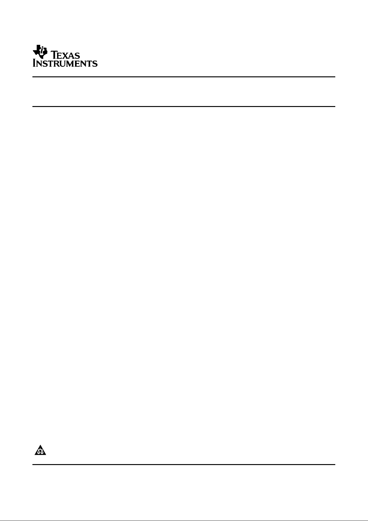
Output
Formatter
ROUT[9:0]
GOUT[9:0]
Host
Interface
Timing Processor
and Clock generation
RIN_1
SCL
SDA
I2CA
GIN_1
BIN_1
Clamp
Clamp
Clamp
PGA
PGA
PGA
10−bit
ADC
10−bit
ADC
10−bit
ADC
HSYNC_A
VSYNC_A
COAST
CLAMP
FILT1
SOGIN_1
RESETB
PWDN
BOUT[9:0]
SOGOUT
HSOUT
VSOUT
DATACLK
RIN_2
GIN_2
BIN_2
EXT_CLK
SOGIN_2
HSYNC_B
VSYNC_B
FILT2
RIN_3
GIN_3
GIN_4
SOGIN_3
BIN_3
TVP7000
SLES143 – SEPTEMBER 2005
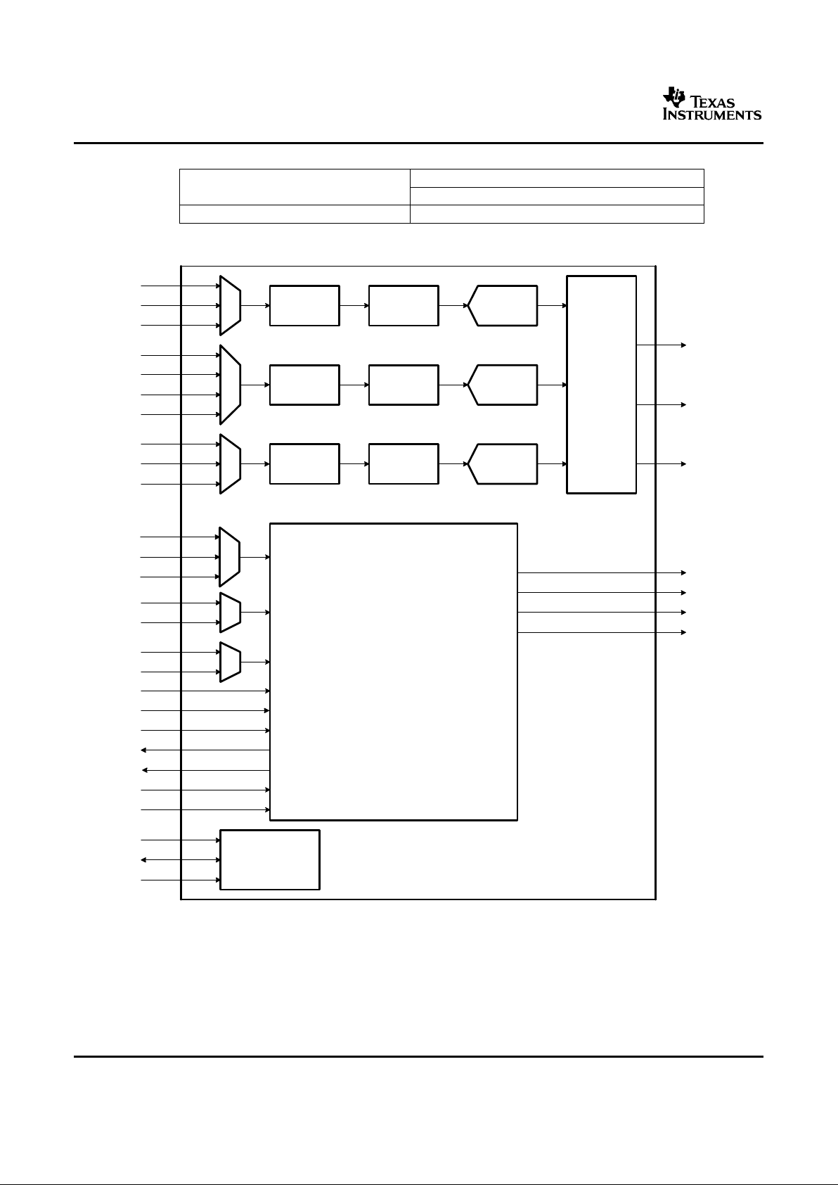
ORDERING INFORMATION
PACKAGED DEVICES
T
A
100-PIN PLASTIC FLATPACK PowerPAD™
0 ° C to 70 ° C TVP7000PZP
FUNCTIONAL BLOCK DIAGRAM
2
www.ti.com
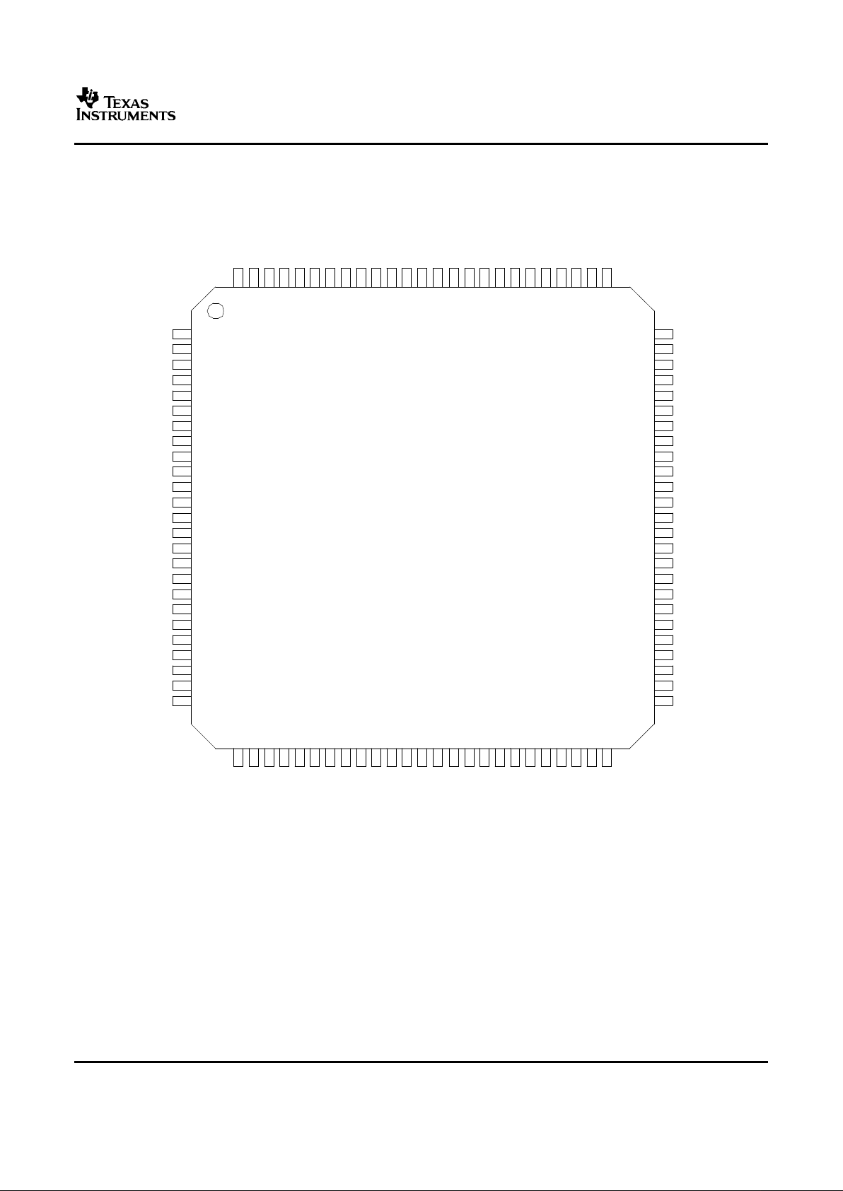
TERMINAL ASSIGNMENTS
TVP7000
100−Pin TQFP Package
(Top View)
SOGIN_1
GIN_1
A18GND
A18VDD
A18GND
A18VDD
A18VDD
A18GND
RIN_3
RIN_2
RIN_1
A33GND
A33VDD
A33VDD
A33GND
BIN_3
BIN_2
BIN_1
A18VDD
A18GND
NSUB
TEST
VSOUT
HSOUT
SOGOUT
IOVDD
IOGND
B_9
B_8
B_7
B_6
B_5
B_4
B_3
B_2
B_1
B_0
DVDD
GND
IOVDD
IOGND
G_9
G_8
G_7
G_6
G_5
G_4
G_3
G_2
SDA
SCL
I2CA
TMS
RESETB
PWDN
DVDD
GND
IOGND
IOVDD
R_0
R_1
R_2
R_3
R_4
IOGND
R_5
R_6
R_7
R_8
R_9
IOGND
IOVDD
G_0
G_1
GIN_2
SOGIN_2
GIN_3
SOGIN_3
GIN_4
A33GND
A33VDD
A33VDD
A33GND
NSUB
PLL_A18GND
PLL_F
FILT2
FILT1
PLL_A18GND
PLL_A18VDD
PLL_A18VDD
PLL_A18GND
HSYNC_B
HSYNC_A
EXT_CLK
VSYNC_B
VSYNC_A
COAST
CLAMP
1
2
3
4
5
6
7
8
9
10
11
12
13
14
15
16
17
18
19
20
21
22
23
24
25
75
74
73
72
71
70
69
68
67
66
65
64
63
62
61
60
59
58
57
56
55
54
53
52
51
100
9998979695949392919089888786858483828180797877
76
26272829303132333435363738394041424344454647484950
TVP7000
SLES143 – SEPTEMBER 2005
3
www.ti.com
TVP7000
SLES143 – SEPTEMBER 2005
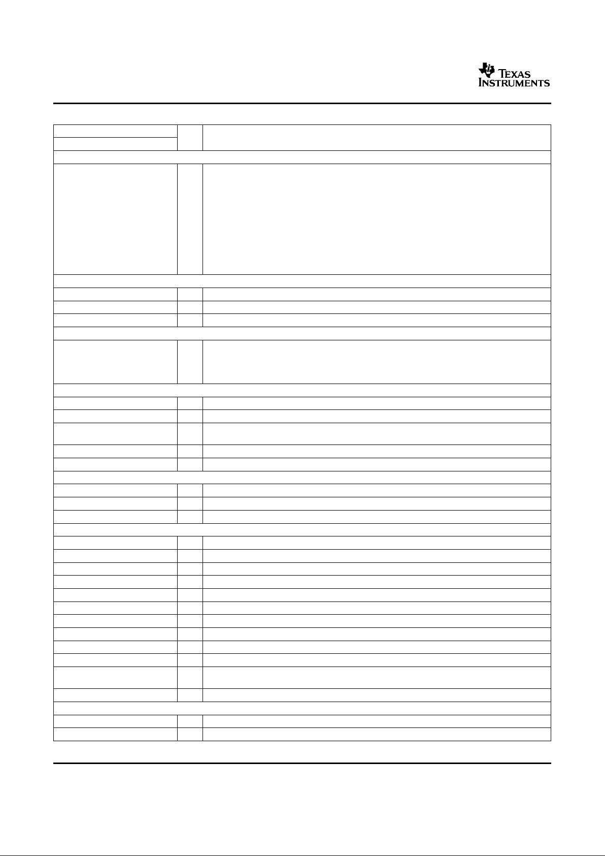
TERMINAL FUNCTIONS
TERMINAL
I/O DESCRIPTION
NAME NO.
ANALOG VIDEO
Analog video input for R/Pr 1
RIN_1 11 I Analog video input for R/Pr 2
RIN_2 10 I Analog video input for R/Pr 3
RIN_3 9 I Analog video input for G/Y 1
GIN_1 2 I Analog video input for G/Y 2
GIN_2 100 I Analog video input for G/Y 3
GIN_3 98 I Analog video input for G/Y 4
GIN_4 96 I Analog video input for B/Pb 1
BIN_1 18 I Analog video input for B/Pb 2
BIN_2 17 I Analog video input for B/Pb 3
BIN_3 16 I The inputs must be AC coupled. The recommended coupling capacitor is 0.1 µ F. Unused analog
inputs should be connected to ground using a 10 nF capacitor.
CLOCK SIGNALS
DATACLK 28 O Data clock output
EXT_CLK 80 I External clock input for free running mode
TEST 22 O Internal 5 MHz clock output, coast output, high-Z, or SOG output
DIGITAL VIDEO
ROUT [9:0] 55–59, 61–65 O Digital video output of R/Cr, ROUT [9] is MSB.
GOUT [9:0] 43-52 O Digital video output of G/Y, GOUT [9] is MSB.
BOUT [9:0] 29-38 O Digital video output of B/Cb, BOUT [9] is MSB. For a 4:2:2 mode BOUT outputs CbCr data.
Unused outputs can be left unconnected.
MISCELLANEOUS SIGNALS
PWDN 70 I Power down input. 1: Power down 0: Normal mode
RESETB 71 I Reset input, active low
Test Mode Select input. Used to enable JTAG test mode. Active high. Normal mode, this terminal
TMS 72 I
should be connected to a ground.
FILT1 87 O External filter connection for PLL. The recommended capacitor is 0.1 µ F. see Figure 4
FILT2 88 O External filter connection for PLL. The recommended capacitor is 4.7 nF. See Figure 4
HOST INTERFACE
I2C A 73 I I2C Address input
SCL 74 I I2C Clock input
SDA 75 I/O I2C Data bus
POWER SUPPLIES
NSUB 21, 91 I Substrate ground. Connect to analog ground.
A33VDD 13, 14, 93, 94 I Analog power. Connect to 3.3 V.
A33GND 12, 15, 92, 95 I Analog 3.3 V return. Connect to Ground.
A18GND 3, 5, 8, 20 I Analog 1.8V return. Connect to Ground
A18VDD 4, 6, 7, 19 I Analog power. Connect to 1.8 V.
PLL_A18VDD 84, 85 I PLL analog power. Connect to 1.8 V.
PLL_F 89 I PLL filter internal supply connection
PLL_A18GND 83, 86, 90 I PLL analog power return. Connect to Ground.
GND 40, 68 I Digital return. Connect to Ground.
DVDD 39, 69 I Digital power. Connect to 1.8 V
27, 42, 54, 60, Digital power return. Connect to Ground.
IOGND I
67
IOVDD 26, 41, 53, 66 I Digital power. Connect to 3.3 V or less for reduced noise.
SYNC SIGNALS
CLAMP 76 I External Clamp input. Unused inputs can be connected to ground.
COAST 77 I External PLL COAST signal input. Unused inputs can be connected to ground
4
www.ti.com
ABSOLUTE MAXIMUM RATINGS
RECOMMENDED OPERATING CONDITIONS
TVP7000
SLES143 – SEPTEMBER 2005
TERMINAL FUNCTIONS (continued)
TERMINAL
I/O DESCRIPTION
NAME NO.
VSYNC_A 78 I Vertical sync input A
VSYNC_B 79 I Vertical sync input B. Unused inputs can be connected to ground.
HSYNC_A 81 I Horizontal Sync input A
HSYNC_B 82 I Horizontal Sync input B. Unused inputs can be connected to ground.
SOGIN1 1 I Sync-on-green input 1
SOGIN2 99 I Sync-on-green input 2
SOGIN3 97 i Sync-on-green input 3. Unused inputs should be connected to ground using a 10 nF capacitor.
VSOUT 23 O Vertical sync output
HSOUT 24 O Horizontal sync output
SOGOUT 25 O Sync-on-green slicer output
over operating free-air temperature range (unless otherwise noted)
(1)
UNIT
IOVDD to IOGND –0.5 V to 4.5 V
DVDD to GND –0.5 V to 2.3 V
Supply voltage range
PLL_A18VDD to PLL_A18GND and A18VDD to A18GND –0.5 V to 2.3 V
A33VDD to A33GND – 0.5 V to 4.5 V
Digital input voltage range VI to GND –0.5 V to 4.5 V
Analog input voltage range AI to A33GND –0.2 V to 2.3 V
Digital output voltage range VO to GND –0.5 V to 4.5 V
TA Operating free-air temperature 0 ° C to 70 ° C
Tstg Storage temperature –65 ° C to 150 ° C
(1) Stresses beyond those listed under absolute maximum ratings may cause permanent damage to the device. These are stress ratings
only and functional operation of the device at these or any other conditions beyond those indicated under recommended operating
conditions is not implied. Exposure to absolute–maximum–rated conditions for extended periods may affect device reliability.
over operating free-air temperature range, TA= 0 ° C to 70 ° C (unless otherwise noted)
MIN NOM MAX UNIT
IOVDD Digital I/O supply voltage 3.0 3.3 3.6 V
DVDD Digital supply voltage 1.70 1.8 1.9 V
PLL_A18VDD Analog PLL supply voltage 1.70 1.8 1.9 V
A18VDD Analog supply voltage 1.70 1.8 1.9 V
A33VDD Analog supply voltage 3.0 3.3 3.6 V
V
I(P–P)
Analog input voltage (ac–coupling necessary) 0.5 2.0 V
V
IH
Digital input voltage high 0.7 IOVDD V
V
IL
Digital input voltage low 0.3 IOVDD V
I
OH
High–level output current 2 mA
I
OL
Low–level output current –2 mA
I
OH_DATACLK
DATACLK high–level output current 4 mA
I
OL_DATACLK
DATACLK low–level output current –4 mA
T
A
Operating free–air temperature 0 70 ° C
5
www.ti.com
ELECTRICAL CHARACTERISTICS
TVP7000
SLES143 – SEPTEMBER 2005
IOVDD = 3.3 V, DVDD = 1.8 V, PLL_A18VDD = 1.8 V, A18VDD = 1.8 V, A33VDD = 3.3 V, TA= 25 ° C
PARAMETER TEST CONDITIONS MIN TYP
(1)
MAX
(2)
UNIT
POWER SUPPLY
I
IOVDDD
3.3-V supply current 78.75 MHz 80 130 mA
I
DVDD
1.8-V supply current 78.75 MHz 253 260 mA
P
TOT
Total power dissipation, normal mode 78.75 MHz 719 897 mW
I
IOVDDD
3.3-V supply current 108 MHz 101 160 mA
I
DVDD
1.8-V supply current 108 MHz 261 275 mA
P
TOT
Total power dissipation, normal mode 108 MHz 803 1023 mW
I
IOVDDD
3.3-V supply current 148.5 MHz 128 240 mA
I
DVDD
1.8-V supply current 148.5 MHz 250 280 mA
P
TOT
Total power dissipation, normal mode 148.5 MHz 872 1296 mW
P
DOWN
Total power dissipation, power–down mode 1 mW
(1) SMPTE color bar RGB input pattern used.
(2) Worst case vertical line RGB input pattern used.
6
www.ti.com
ELECTRICAL CHARACTERISTICS
TVP7000
SLES143 – SEPTEMBER 2005
IOVDD = 3.3 V, DVDD = 1.8 V ± 0.1, PLL_A18VDD = 1.8 V ± 0.1, A18VDD = 1.8 V ± 0.1, A33VDD = 3.3 V, TA= 0 ° C to 70 ° C
(unless otherwise noted)
PARAMETER TEST CONDITIONS MIN TYP MAX UNIT
ANALOG INTERFACE
Input voltage range By design 0.5 1.0 2.0 Vpp
Z
I
Input impedance, analog video inputs By design 500 k Ω
DIGITAL LOGIC INTERFACE
C
i
Input capacitance By design 10 pF
Z
i
Input impedance By design 500 k Ω
V
OH
Output voltage high IOH= 2 mA 0.8 IOVDD V
V
OL
Output voltage low IOL= –2 mA 0.2 IOVDD V
V
OH_SCLK
DATACLK output voltage high IOH= 4 mA 0.8 IOVDD V
V
OL_SCLK
DATACLK output voltage low IOH= –2 mA 0.2 IOVDD V
V
IH
High-level input voltage By design 0.7 IOVDD V
V
IL
Low-level input voltage By design 0.3 IOVDD V
A/D CONVERTERS
Conversion rate 12 150 MSPS
10 bit, 110 MHz -1 ± 0.5 +1
DNL DC differential nonlinearity LSB
8 bit, 150 MHz -1 ± 0.5 +1
10 bit, 110 MHz -4 ± 1 +4
INL DC integral nonlinearity LSB
8 bit, 150 MHz -4 ± 1 +4
Missing code 8 bit, 150 MHz none
SNR Signal-to-noise ratio 10 MHz, 1.0 V
P–P
at 110 52 dB
MSPS
Analog bandwidth By design 500 MHz
PLL
Clock jitter 500 ps
Phase adjustment 11.6 degree
VCO frequency range 12 150 MHz
7
www.ti.com
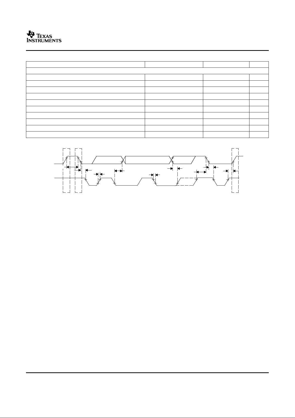
TIMING REQUIREMENTS
DATACLK
t1
t2
t3
Valid DataR, R, B, HSOUT Valid Data
TVP7000
SLES143 – SEPTEMBER 2005
PARAMETER TEST CONDITIONS
(1)
MIN TYP MAX UNIT
CLOCKS, VIDEO DATA, SYNC TIMING
Duty cycle DATACLK 50%
t
1
DATACLK rise time 10% to 90% 1 ns
t
2
DATACLK fall time 90% to 10% 1 ns
t
3
Output delay time 1.5 3.5 ns
(1) Measured with a load of 15 pF.
Figure 1. Clock, Video Data, and Sync Timing
8
www.ti.com
TIMING REQUIREMENTS
SDA
t1
t6
t7
t2
t8
t3
t4
t6
SCL
Data
Stop Start Stop
t5
TVP7000
SLES143 – SEPTEMBER 2005
PARAMETER TEST CONDITIONS MIN TYP MAX UNIT
I2C HOST PORT TIMING
t
1
Bus free time between STOP and START Specified by design 1.3 µ s
t
2
Setup time for a (repeated) START condition Specified by design 0.6 µ s
t
3
Hold time (repeated) START condition Specified by design 0.6 µ s
t
4
Setup time for a STOP condition Specified by design 0.6 ns
t
5
Data setup time Specified by design 100 ns
t
6
Data hold time Specified by design 0 0.9 µ s
t
7
Rise time SDA and SCL signal Specified by design 250 ns
t
8
Fall time SDA and SCL signal Specified by design 250 ns
C
b
Capacitive load for each bus line Specified by design 400 pF
f
12C
I2C clock frequency Specified by design 400 kHz
Figure 2. I2C Host Port Timing
9

www.ti.com
FUNCTIONAL DESCRIPTION
Analog Channel
TVP7000
SLES143 – SEPTEMBER 2005
The TVP7000 contains three identical analog channels that are independently programmable. Each channel
consists of a clamping circuit, a programmable gain amplifier, automatic offset control and an A/D converter.
Analog Input Switch Control
TVP7000 has 3 analog channels that accept up to 10 video inputs. The user can configure the internal analog
video switches via the I2C interface. The 10 analog video inputs can be used for different input configurations
some of which are:
• Up to 10 selectable individual composite video inputs
• Up to 2 selectable RGB graphics inputs
• Up to 3 selectable YPbPr video HD/SD inputs
The input selection is performed by the input select register at I2C subaddress 0 × 19 and 0 × 1A (see Input Mux
Select 1 and Input Mux Select 2)
Analog Input Clamping
An internal clamping circuit restores the AC-coupled video/graphic signal to a fixed DC level. The clamping circuit
provides line-by-line restoration of the signal black level to a fixed DC reference voltage. The selection between
bottom and mid level clamping is performed by I2C subaddress 0 × 10 (see Sync On_Green Threshold)
The internal clamping time can be adjusted by I2C clamp start and width registers at subaddress 0 × 05 and 0 × 06
(see Clamp Start and Clamp Width)
Programmable Gain Amplifier (PGA)
The TVP7000 PGA can scale a signal with a voltage-input compliance of 0.5-Vpp to 2-Vpp to a full-scale 10-bit
A/D output code range. A 4-bit code sets the coarse gain (Red Coarse Gain, Green Coarse Gain, Blue Coarse
Gain) with individual adjustment per channel. Minimum gain corresponds to a code 0 × 0 (2-Vpp full-scale input,
–6 dB gain) while maximum gain corresponds to code 0 × F (0.5-Vpp full-scale, +6 dB gain). TVP7000 also has
8-bit fine gain control (Red Fine Gain, Green Fine Gain, Blue Fine Gain) for RGB independently ranging from 1
to 2. For a normal PC graphics input, the fine gain will be used mostly.
Programmable Offset Control and Automatic Level Control (ALC)
The TVP7000 supports a programmable offset control for RGB independently. A 6-bit code sets the coarse offset
(Red Coarse Offset, Green Coarse Offset, Blue Coarse Offset) with individual adjustment per channel. The
coarse offset ranges from –32 LSB to +31 LSB. The coarse offset registers apply before the ADC. A 10-bit fine
offset registers (Red Fine Offset, Green Fine Offset, Blue Fine Offset) apply after the ADC. The fine offset ranges
from –512 LSB to +511 LSB.
ALC circuit maintains the level of the signal to be set at a value which is programmed at fine offset I2C register. It
consists of pixel averaging filter and feedback loop. This ALC function can be enabled or disabled by I2C register
address at 0 × 26. ALC circuit needs a timing pulse generated internally but user should program the position
properly. The ALC pulse must be positioning after the clamp pulse. The position of ALC pulse is controlled by
ALC placement I2C register at address 0 × 31. This is available only for internal ALC pulse timing. For external
clamp, the timing control of clamp is not applicable so the ALC pulse control is also not applicable. Therefore it is
suggested to keep the external clamp pulse as long as possible. ALC is applied as same position of external
clamp pulse.
A/D Converters
All ADCs have a resolution of 10-bits and can operate up to 150 MSPS. All A/D channels receive an identical
clock from the on-chip phase-locked loop (PLL) at a frequency between 12 MHz and 150 MHz. All ADC
reference voltages are generated internally. Also the external sampling clock can be used.
10
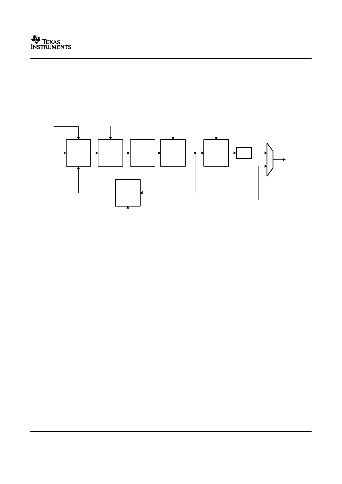
www.ti.com
COAST
HSYNC
Phase
Detector
PLL Control
Register 0x03
Bit [5:3]
PLL Control
Register 0x03
Bit [7:6]
Phase Select
Register 0x04
Bit [7:3]
Charge
Pump
VCO
Phase
Select
Divider
ADC
Sampling
CLK
External
Clock
PLL Divide
Register 0x01
and 0x02
Bit [11:0]
Loop
Filter
÷ N
N = 1 or 2
TVP7000
SLES143 – SEPTEMBER 2005
Analog PLL
The analog PLL generates a high-frequency internal clock used by the ADC sampling and data clocking out to
derive the pixel output frequency with programmable phase. The reference signal for this PLL is the horizontal
sync signal supplied on the HSYNC input or from extracted horizontal sync of sync slicer block for embedded
sync signals. The analog PLL consisted of phase detector, loop filter, voltage controlled oscillator (VCO), divider
and phase select. The analog block diagram is shown at Figure 3 .
Figure 3. PLL Block Diagram
The COAST signal is used to allow the PLL to keep running at the same frequency, in the absence of the
incoming HSYNC signal or disordered HSYNC period. This is useful during the vertical sync period, or any other
time that the HSYNC is not available.
There are several PLL controls to produce the correct sampling clock. The 12-bit divider register is
programmable to select exact multiplication number to generate the pixel clock in the range of 12 MHz to 150
MHz. The 3-bit loop filter current control register is to control the charge pump current that drives the low-pass
loop filter. The applicable current values are listed in the Table 1 .
The 2-bit VCO range control is to improve the noise performance of the TVP7000. The frequency ranges for the
VCO are shown in Table 1 . The phase of the PLL generated clock can be programmed in 32 uniform steps over
a single clock period (360/32=11.25 degrees phase resolution) so that the sampling phase of the ADC can be
accurately controlled.
In addition to sourcing the ADC channel clock from the PLL, an external pixel clock can be used (from pin 80).
The PLL characteristics are determined by the loop filter design, by the PLL charge pump current, and by the
VCO range setting. The loop filter design is shown in Figure 4 . Supported settings of VCO range and charge
pump current for VESA standard display modes are listed in Table 1 .
11
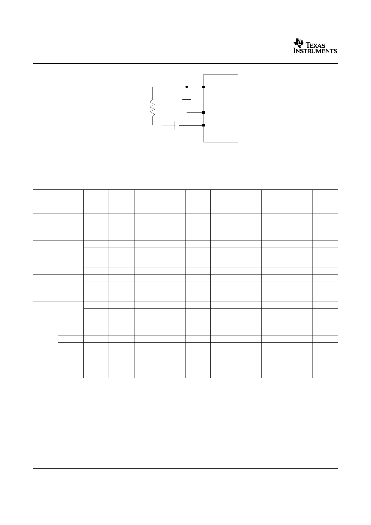
www.ti.com
0.1 µF
4.7 nF
1.5 kΩ
TVP7000
PLL_F
FILT2
FILT1
89
88
87
TVP7000
SLES143 – SEPTEMBER 2005
Figure 4. PLL Loop Filter
Table 1. Recommended VCO Range and Charge Pump Current Settings for Supporting Standard Display
Formats
STANDARD RESOL- REFRESH HORIZON- PIXEL RATE PLL Divider PLLDIV PLLDIV LSB Reg 03h Output Div- VCO CP CUR-
UTION RATE TAL (MHz) Total MSB Reg Reg 02h ider Reg RANGE Reg RENT Reg
FRE- pix/line 01h [11:4] 04h [0] 03h [7:6] 03h [5:3]
QUENCY
(kHz)
VGA 640 × 480 60 Hz 31.5 25.175 1600(2 × ) 64h 00h 68h 1 Low (01b) 101b
72 Hz 37.9 31.5 1664(2 × ) 68h 00h 58h 1 Low (01b) 011b
75 Hz 37.5 31.5 1680(2 × ) 69h 00h 58h 1 Low (01b) 011b
85 Hz 43.3 36 832 34h 00h 68h 0 Low (01b) 101b
SVGA 800 × 600 56 Hz 35.1 36 1024 40h 00h 68h 0 Low (01b) 101b
60 Hz 37.9 40 1056 42h 00h 68h 0 Low (01b) 101b
72 Hz 48.1 50 1040 41h 00h 68h 0 Low (01b) 101b
75 Hz 46.9 49.5 1056 42h 00h 68h 0 Low (01b) 101b
85 Hz 53.7 56.25 1048 41h 80h 68h 0 Low (01b) 101b
XGA 1024 × 768 60 Hz 48.4 65 1344 54h 00h 58h 0 Low (01b) 011b
70 Hz 56.5 75 1328 53h 00h A8h 0 Med (10b) 101b
75 Hz 60 78.75 1312 52h 00h A8h 0 Med (10b) 101b
85 Hz 68.7 94.5 1376 56h 00h A8h 0 Med (10b) 101b
SXGA 1280 × 1024 60 Hz 64 108 1688 69h 80h A8h 0 Med (10b) 101b
75 Hz 80 135 1688 69h 80h 98h 0 Med (10b) 011b
Video 720 × 480p 60 Hz 31.468 27 1716(2 × ) 6Bh 40h 68h 1 Low (01b) 101b
720 × 576p 50 Hz 31.25 27 1728(2 × ) 6Ch 00h 68h 1 Low (01b) 101b
1280 × 720p 60 Hz 45 74.25 1650 67h 20h A8h 0 Med (10b) 101b
1280 × 720p 50 Hz 37.5 74.25 1980 7Bh C0h A8h 0 Med (10b) 101b
1920 × 1080i 60 Hz 33.75 74.25 2200 89h 80h A8h 0 Med (10b) 101b
1920 × 1080i 50 Hz 28.125 74.25 2640 A5h 00h A8h 0 Med (10b) 101b
1920 × 60 Hz 67.5 148.5 2200 89h 80h D8h 0 High (11b) 011b
1080p
1920 × 50 Hz 56.25 148.5 2640 A5h 00h D8h 0 High (11b) 011b
1080p
Sync Slicer
TVP7000 includes a circuit that compares the input signal on Green channel to a level 150mV (typical value)
above the clamped level (sync tip). The slicing level is programmable by I2C register subaddress at 0x10. The
digital output of the composite sync slicer is available on the SOGOUT pin.
Sync Separator
The sync separator automatically extracts VSYNC and HSYNC from the sliced composite sync input supplied at
the SOG input. The G or Y input containing the composite sync must be AC coupled to the SOG input pin using
a 10-nF capacitor. Support for PC graphics, SDTV, and HDTV up to 1080p is provided.
12