

Page 1

现货库存、技术资料、百科信息、热点资讯,精彩尽在鼎好!
TVP6000C
Data Manual
NTSC/PAL Digital Video Encoder
SLAS184
July 1998
Printed on Recycled Paper
Page 2

IMPORTANT NOTICE
T exas Instruments and its subsidiaries (TI) reserve the right to make changes to their products or to discontinue
any product or service without notice, and advise customers to obtain the latest version of relevant information
to verify, before placing orders, that information being relied on is current and complete. All products are sold
subject to the terms and conditions of sale supplied at the time of order acknowledgement, including those
pertaining to warranty, patent infringement, and limitation of liability.
TI warrants performance of its semiconductor products to the specifications applicable at the time of sale in
accordance with TI’s standard warranty. Testing and other quality control techniques are utilized to the extent
TI deems necessary to support this warranty . Specific testing of all parameters of each device is not necessarily
performed, except those mandated by government requirements.
CERT AIN APPLICATIONS USING SEMICONDUCTOR PRODUCTS MAY INVOLVE POTENTIAL RISKS OF
DEATH, PERSONAL INJURY, OR SEVERE PROPERTY OR ENVIRONMENTAL DAMAGE (“CRITICAL
APPLICATIONS”). TI SEMICONDUCTOR PRODUCTS ARE NOT DESIGNED, AUTHORIZED, OR
WARRANTED TO BE SUITABLE FOR USE IN LIFE-SUPPORT DEVICES OR SYSTEMS OR OTHER
CRITICAL APPLICA TIONS. INCLUSION OF TI PRODUCTS IN SUCH APPLICATIONS IS UNDERST OOD TO
BE FULLY AT THE CUSTOMER’S RISK.
In order to minimize risks associated with the customer’s applications, adequate design and operating
safeguards must be provided by the customer to minimize inherent or procedural hazards.
TI assumes no liability for applications assistance or customer product design. TI does not warrant or represent
that any license, either express or implied, is granted under any patent right, copyright, mask work right, or other
intellectual property right of TI covering or relating to any combination, machine, or process in which such
semiconductor products or services might be or are used. TI’s publication of information regarding any third
party’s products or services does not constitute TI’s approval, warranty or endorsement thereof.
Copyright 1998, Texas Instruments Incorporated
Page 3

Contents
Section Title Page
1 Introduction 1–1. . . . . . . . . . . . . . . . . . . . . . . . . . . . . . . . . . . . . . . . . . . . . . . . . . . . . . . . . . . . . . .
1.1 Features 1–1. . . . . . . . . . . . . . . . . . . . . . . . . . . . . . . . . . . . . . . . . . . . . . . . . . . . . . . . . . . . . .
1.2 Applications 1–2. . . . . . . . . . . . . . . . . . . . . . . . . . . . . . . . . . . . . . . . . . . . . . . . . . . . . . . . . . .
1.3 Functional Block Diagram 1–2. . . . . . . . . . . . . . . . . . . . . . . . . . . . . . . . . . . . . . . . . . . . . . .
1.4 Terminal Assignments 1–3. . . . . . . . . . . . . . . . . . . . . . . . . . . . . . . . . . . . . . . . . . . . . . . . . .
1.5 Ordering Information 1–4. . . . . . . . . . . . . . . . . . . . . . . . . . . . . . . . . . . . . . . . . . . . . . . . . . .
1.6 Terminal Functions 1–4. . . . . . . . . . . . . . . . . . . . . . . . . . . . . . . . . . . . . . . . . . . . . . . . . . . . .
2 Detailed Description 2–1. . . . . . . . . . . . . . . . . . . . . . . . . . . . . . . . . . . . . . . . . . . . . . . . . . . . . . .
2.1 Initialization 2–1. . . . . . . . . . . . . . . . . . . . . . . . . . . . . . . . . . . . . . . . . . . . . . . . . . . . . . . . . . .
2
2.2 I
2.3 Data Manager 2–4. . . . . . . . . . . . . . . . . . . . . . . . . . . . . . . . . . . . . . . . . . . . . . . . . . . . . . . . .
2.4 Scaling Processor 2–5. . . . . . . . . . . . . . . . . . . . . . . . . . . . . . . . . . . . . . . . . . . . . . . . . . . . .
2.5 Video Encoder 2–6. . . . . . . . . . . . . . . . . . . . . . . . . . . . . . . . . . . . . . . . . . . . . . . . . . . . . . . . .
2.6 Closed Caption 2–9. . . . . . . . . . . . . . . . . . . . . . . . . . . . . . . . . . . . . . . . . . . . . . . . . . . . . . . .
2.7 Clock Generation 2–11. . . . . . . . . . . . . . . . . . . . . . . . . . . . . . . . . . . . . . . . . . . . . . . . . . . . .
2.8 Analog Output 2–11. . . . . . . . . . . . . . . . . . . . . . . . . . . . . . . . . . . . . . . . . . . . . . . . . . . . . . . .
2.9 Video Port Interface 2–12. . . . . . . . . . . . . . . . . . . . . . . . . . . . . . . . . . . . . . . . . . . . . . . . . . .
2.10 Modes of Operation 2–13. . . . . . . . . . . . . . . . . . . . . . . . . . . . . . . . . . . . . . . . . . . . . . . . . . .
2.11 Register Descriptions 2–15. . . . . . . . . . . . . . . . . . . . . . . . . . . . . . . . . . . . . . . . . . . . . . . . . .
C Interface 2–3. . . . . . . . . . . . . . . . . . . . . . . . . . . . . . . . . . . . . . . . . . . . . . . . . . . . . . . . . .
2.5.1 Luminance Encoding 2–6. . . . . . . . . . . . . . . . . . . . . . . . . . . . . . . . . . . . . . . . . . .
2.5.2 Luminance Low-Pass and Interpolation Filter 2–6. . . . . . . . . . . . . . . . . . . . . .
2.5.3 Cross Color Reduction Filter 2–8. . . . . . . . . . . . . . . . . . . . . . . . . . . . . . . . . . . .
2.5.4 Chrominance Encoding 2–8. . . . . . . . . . . . . . . . . . . . . . . . . . . . . . . . . . . . . . . .
2.9.1 RCV1 2–12. . . . . . . . . . . . . . . . . . . . . . . . . . . . . . . . . . . . . . . . . . . . . . . . . . . . . . .
2.9.2 RCV2 2–12. . . . . . . . . . . . . . . . . . . . . . . . . . . . . . . . . . . . . . . . . . . . . . . . . . . . . . .
2.9.3 RCM1 2–12. . . . . . . . . . . . . . . . . . . . . . . . . . . . . . . . . . . . . . . . . . . . . . . . . . . . . . .
2.9.4 RCM2 2–13. . . . . . . . . . . . . . . . . . . . . . . . . . . . . . . . . . . . . . . . . . . . . . . . . . . . . . .
2.10.1 Master Mode 2–13. . . . . . . . . . . . . . . . . . . . . . . . . . . . . . . . . . . . . . . . . . . . . . . . .
2.10.2 Slave Mode 2–13. . . . . . . . . . . . . . . . . . . . . . . . . . . . . . . . . . . . . . . . . . . . . . . . . .
2.10.3 Demand Mode 2–14. . . . . . . . . . . . . . . . . . . . . . . . . . . . . . . . . . . . . . . . . . . . . . .
2.10.4 Genlock Mode 2–14. . . . . . . . . . . . . . . . . . . . . . . . . . . . . . . . . . . . . . . . . . . . . . .
2.1 1.1 DEV_ID 2–17. . . . . . . . . . . . . . . . . . . . . . . . . . . . . . . . . . . . . . . . . . . . . . . . . . . . .
2.1 1.2 REV_ID 2–17. . . . . . . . . . . . . . . . . . . . . . . . . . . . . . . . . . . . . . . . . . . . . . . . . . . . .
2.1 1.3 STA TUS 2–17. . . . . . . . . . . . . . . . . . . . . . . . . . . . . . . . . . . . . . . . . . . . . . . . . . . . .
2.1 1.4 F_CONTROL 2–18. . . . . . . . . . . . . . . . . . . . . . . . . . . . . . . . . . . . . . . . . . . . . . . .
2.1 1.5 C_PHASE 2–19. . . . . . . . . . . . . . . . . . . . . . . . . . . . . . . . . . . . . . . . . . . . . . . . . . .
2.1 1.6 GAIN_U 2–19. . . . . . . . . . . . . . . . . . . . . . . . . . . . . . . . . . . . . . . . . . . . . . . . . . . . .
2.1 1.7 GAIN_V 2–19. . . . . . . . . . . . . . . . . . . . . . . . . . . . . . . . . . . . . . . . . . . . . . . . . . . . .
2.1 1.8 BLACK_LEVEL 2–19. . . . . . . . . . . . . . . . . . . . . . . . . . . . . . . . . . . . . . . . . . . . . .
2.1 1.9 BLANK_LEVEL 2–20. . . . . . . . . . . . . . . . . . . . . . . . . . . . . . . . . . . . . . . . . . . . . .
iii
Page 4

Contents (Continued)
Section Title Page
2.11.10 GAIN_Y 2–20. . . . . . . . . . . . . . . . . . . . . . . . . . . . . . . . . . . . . . . . . . . . . . . . . . . . .
2.1 1.1 1 X_COLOR 2–20. . . . . . . . . . . . . . . . . . . . . . . . . . . . . . . . . . . . . . . . . . . . . . . . . . .
2.1 1.12 M_CONTROL 2–21. . . . . . . . . . . . . . . . . . . . . . . . . . . . . . . . . . . . . . . . . . . . . . . .
2.1 1.13 BST AMP 2–21. . . . . . . . . . . . . . . . . . . . . . . . . . . . . . . . . . . . . . . . . . . . . . . . . . . .
2.11.14 S_CARR1, 2, 3, 4 2–22. . . . . . . . . . . . . . . . . . . . . . . . . . . . . . . . . . . . . . . . . . . .
2.1 1.15 LINE21_O0 2–23. . . . . . . . . . . . . . . . . . . . . . . . . . . . . . . . . . . . . . . . . . . . . . . . . .
2.1 1.16 LINE21_O1 2–23. . . . . . . . . . . . . . . . . . . . . . . . . . . . . . . . . . . . . . . . . . . . . . . . . .
2.1 1.17 LINE21_E0 2–23. . . . . . . . . . . . . . . . . . . . . . . . . . . . . . . . . . . . . . . . . . . . . . . . . .
2.1 1.18 LINE21_E1 2–23. . . . . . . . . . . . . . . . . . . . . . . . . . . . . . . . . . . . . . . . . . . . . . . . . .
2.1 1.19 LN_SEL 2–23. . . . . . . . . . . . . . . . . . . . . . . . . . . . . . . . . . . . . . . . . . . . . . . . . . . . .
2.1 1.20 SYN_CTRL0 2–24. . . . . . . . . . . . . . . . . . . . . . . . . . . . . . . . . . . . . . . . . . . . . . . . .
2.1 1.21 RCM_L21 2–26. . . . . . . . . . . . . . . . . . . . . . . . . . . . . . . . . . . . . . . . . . . . . . . . . . .
2.1 1.22 HTRIGGER0 2–28. . . . . . . . . . . . . . . . . . . . . . . . . . . . . . . . . . . . . . . . . . . . . . . . .
2.1 1.23 HTRIGGER1 2–28. . . . . . . . . . . . . . . . . . . . . . . . . . . . . . . . . . . . . . . . . . . . . . . . .
2.1 1.24 VTRIGGER 2–28. . . . . . . . . . . . . . . . . . . . . . . . . . . . . . . . . . . . . . . . . . . . . . . . . .
2.1 1.25 BMRQ 2–29. . . . . . . . . . . . . . . . . . . . . . . . . . . . . . . . . . . . . . . . . . . . . . . . . . . . . .
2.1 1.26 EMRQ 2–29. . . . . . . . . . . . . . . . . . . . . . . . . . . . . . . . . . . . . . . . . . . . . . . . . . . . . .
2.1 1.27 BEMRQ 2–29. . . . . . . . . . . . . . . . . . . . . . . . . . . . . . . . . . . . . . . . . . . . . . . . . . . . .
2.1 1.28 BRCV 2–29. . . . . . . . . . . . . . . . . . . . . . . . . . . . . . . . . . . . . . . . . . . . . . . . . . . . . . .
2.1 1.29 ERCV 2–30. . . . . . . . . . . . . . . . . . . . . . . . . . . . . . . . . . . . . . . . . . . . . . . . . . . . . . .
2.1 1.30 BERCV 2–30. . . . . . . . . . . . . . . . . . . . . . . . . . . . . . . . . . . . . . . . . . . . . . . . . . . . .
2.1 1.31 FLEN 2–30. . . . . . . . . . . . . . . . . . . . . . . . . . . . . . . . . . . . . . . . . . . . . . . . . . . . . . .
2.1 1.32 FAL 2–30. . . . . . . . . . . . . . . . . . . . . . . . . . . . . . . . . . . . . . . . . . . . . . . . . . . . . . . . .
2.1 1.33 LAL 2–31. . . . . . . . . . . . . . . . . . . . . . . . . . . . . . . . . . . . . . . . . . . . . . . . . . . . . . . . .
2.1 1.34 FLAL 2–31. . . . . . . . . . . . . . . . . . . . . . . . . . . . . . . . . . . . . . . . . . . . . . . . . . . . . . .
2.1 1.35 SYN_CTRL1 2–31. . . . . . . . . . . . . . . . . . . . . . . . . . . . . . . . . . . . . . . . . . . . . . . . .
2.1 1.36 SCM 2–32. . . . . . . . . . . . . . . . . . . . . . . . . . . . . . . . . . . . . . . . . . . . . . . . . . . . . . . .
2.1 1.37 SLPF 2–32. . . . . . . . . . . . . . . . . . . . . . . . . . . . . . . . . . . . . . . . . . . . . . . . . . . . . . .
2.1 1.38 SPPL 2–33. . . . . . . . . . . . . . . . . . . . . . . . . . . . . . . . . . . . . . . . . . . . . . . . . . . . . . .
2.1 1.39 SLPH 2–33. . . . . . . . . . . . . . . . . . . . . . . . . . . . . . . . . . . . . . . . . . . . . . . . . . . . . . .
2.1 1.40 DLPF 2–33. . . . . . . . . . . . . . . . . . . . . . . . . . . . . . . . . . . . . . . . . . . . . . . . . . . . . . .
2.1 1.41 DPPL 2–33. . . . . . . . . . . . . . . . . . . . . . . . . . . . . . . . . . . . . . . . . . . . . . . . . . . . . . .
2.1 1.42 DLPH 2–34. . . . . . . . . . . . . . . . . . . . . . . . . . . . . . . . . . . . . . . . . . . . . . . . . . . . . . .
2.1 1.43 VDT AL 2–34. . . . . . . . . . . . . . . . . . . . . . . . . . . . . . . . . . . . . . . . . . . . . . . . . . . . . .
2.1 1.44 VDT AH 2–34. . . . . . . . . . . . . . . . . . . . . . . . . . . . . . . . . . . . . . . . . . . . . . . . . . . . . .
2.1 1.45 HDT AL 2–34. . . . . . . . . . . . . . . . . . . . . . . . . . . . . . . . . . . . . . . . . . . . . . . . . . . . . .
2.1 1.46 HDT AH 2–35. . . . . . . . . . . . . . . . . . . . . . . . . . . . . . . . . . . . . . . . . . . . . . . . . . . . .
2.1 1.47 VOFS 2–35. . . . . . . . . . . . . . . . . . . . . . . . . . . . . . . . . . . . . . . . . . . . . . . . . . . . . . .
2.1 1.48 HOFS 2–35. . . . . . . . . . . . . . . . . . . . . . . . . . . . . . . . . . . . . . . . . . . . . . . . . . . . . . .
2.1 1.49 NLR 2–35. . . . . . . . . . . . . . . . . . . . . . . . . . . . . . . . . . . . . . . . . . . . . . . . . . . . . . . .
2.11.50 TEST1, TEST2, TEST3 2–35. . . . . . . . . . . . . . . . . . . . . . . . . . . . . . . . . . . . . . .
iv
Page 5

Contents (Continued)
Section Title Page
3 Electrical Characteristics 3–1. . . . . . . . . . . . . . . . . . . . . . . . . . . . . . . . . . . . . . . . . . . . . . . . . .
3.1 Absolute Maximum Ratings Over Operating Free-Air Temperature Range 3–1. . . . .
3.2 Recommended Operating Conditions 3–1. . . . . . . . . . . . . . . . . . . . . . . . . . . . . . . . . . . . .
3.3 DC Electrical Characteristics, T
3.4 AC Electrical Characteristics, T
3.5 Timing Requirements 3–2. . . . . . . . . . . . . . . . . . . . . . . . . . . . . . . . . . . . . . . . . . . . . . . . . . .
3.6 Demand Mode Timing 3–2. . . . . . . . . . . . . . . . . . . . . . . . . . . . . . . . . . . . . . . . . . . . . . . . . .
3.7 Switching Characteristics 3–2. . . . . . . . . . . . . . . . . . . . . . . . . . . . . . . . . . . . . . . . . . . . . . .
A Example Register Settings A–1. . . . . . . . . . . . . . . . . . . . . . . . . . . . . . . . . . . . . . . . . . . . . . . . .
B Mechanical Data B–1. . . . . . . . . . . . . . . . . . . . . . . . . . . . . . . . . . . . . . . . . . . . . . . . . . . . . . . . . . .
= 25°C, DVDD = AVDD = 5 V 3–1. . . . . . . . . . . . . . .
A
= 25°C, DVDD = AVDD = 5 V 3–2. . . . . . . . . . . . . . .
A
List of Illustrations
Figure Title Page
1–1 Terminal Assignments 1–3. . . . . . . . . . . . . . . . . . . . . . . . . . . . . . . . . . . . . . . . . . . . . . . . . . . . . .
2–1 Block Diagram 2–2. . . . . . . . . . . . . . . . . . . . . . . . . . . . . . . . . . . . . . . . . . . . . . . . . . . . . . . . . . . . .
2
2–2 I
C Start and Stop Conditions 2–3. . . . . . . . . . . . . . . . . . . . . . . . . . . . . . . . . . . . . . . . . . . . . . .
2
2–3 I
C Access Cycles 2–3. . . . . . . . . . . . . . . . . . . . . . . . . . . . . . . . . . . . . . . . . . . . . . . . . . . . . . . . .
2
2–4 I
C Write Cycle 2–4. . . . . . . . . . . . . . . . . . . . . . . . . . . . . . . . . . . . . . . . . . . . . . . . . . . . . . . . . . . .
2
2–5 I
C Read Cycle 2–4. . . . . . . . . . . . . . . . . . . . . . . . . . . . . . . . . . . . . . . . . . . . . . . . . . . . . . . . . . . .
2–6 Luma Path Frequency Response 2–7. . . . . . . . . . . . . . . . . . . . . . . . . . . . . . . . . . . . . . . . . . . .
2–7 Luma Cross Color Reduction Filter 2–7. . . . . . . . . . . . . . . . . . . . . . . . . . . . . . . . . . . . . . . . . . .
2–8 Chroma Path Frequency Response 2–9. . . . . . . . . . . . . . . . . . . . . . . . . . . . . . . . . . . . . . . . . .
2–9 NTSC CCIR601 Rate Closed Caption Line 2–10. . . . . . . . . . . . . . . . . . . . . . . . . . . . . . . . . . .
2–10 PAL CCIR601 Pixel Rate Closed Caption Line 2–10. . . . . . . . . . . . . . . . . . . . . . . . . . . . . . .
2–11 NTSC Square Pixel Rate Closed Caption Line 2–11. . . . . . . . . . . . . . . . . . . . . . . . . . . . . . .
2–12 PAL Square Pixel Rate Closed Caption Line 2–11. . . . . . . . . . . . . . . . . . . . . . . . . . . . . . . . .
2–13 Output Filter 2–12. . . . . . . . . . . . . . . . . . . . . . . . . . . . . . . . . . . . . . . . . . . . . . . . . . . . . . . . . . . . .
2–14 Transmission Timing 2–15. . . . . . . . . . . . . . . . . . . . . . . . . . . . . . . . . . . . . . . . . . . . . . . . . . . . .
3–1 Data Setup and Hold Timing 3–3. . . . . . . . . . . . . . . . . . . . . . . . . . . . . . . . . . . . . . . . . . . . . . . . .
3–2 Demand Mode Timing 3–3. . . . . . . . . . . . . . . . . . . . . . . . . . . . . . . . . . . . . . . . . . . . . . . . . . . . . .
v
Page 6

List of Tables
Table Title Page
2–1 16-Bit Video Port YUV 4:2:2 2–5. . . . . . . . . . . . . . . . . . . . . . . . . . . . . . . . . . . . . . . . . . . . . . . . .
2–2 8-Bit Multiplexed Video Port CCIR656 YUV 4:2:2 2–5. . . . . . . . . . . . . . . . . . . . . . . . . . . . . . .
2–3 100/100 Color Bar in Twos Complement 2–5. . . . . . . . . . . . . . . . . . . . . . . . . . . . . . . . . . . . . .
2–4 Master Mode 2–13. . . . . . . . . . . . . . . . . . . . . . . . . . . . . . . . . . . . . . . . . . . . . . . . . . . . . . . . . . . . .
2–5 Crystal Frequencies 2–13. . . . . . . . . . . . . . . . . . . . . . . . . . . . . . . . . . . . . . . . . . . . . . . . . . . . . . .
2–6 Slave Mode Signals 2–14. . . . . . . . . . . . . . . . . . . . . . . . . . . . . . . . . . . . . . . . . . . . . . . . . . . . . . .
2–7 Base Addresses 2–15. . . . . . . . . . . . . . . . . . . . . . . . . . . . . . . . . . . . . . . . . . . . . . . . . . . . . . . . . .
2–8 Register Bit Allocation Map 2–15. . . . . . . . . . . . . . . . . . . . . . . . . . . . . . . . . . . . . . . . . . . . . . . . .
2–9 Input Format and Data Sampling 2–18. . . . . . . . . . . . . . . . . . . . . . . . . . . . . . . . . . . . . . . . . . . .
2–10 Chroma Channel Delays 2–20. . . . . . . . . . . . . . . . . . . . . . . . . . . . . . . . . . . . . . . . . . . . . . . . . .
2–11 Total Horizontal Pixel Selection 2–22. . . . . . . . . . . . . . . . . . . . . . . . . . . . . . . . . . . . . . . . . . . .
2–12 S_CARR Values 2–22. . . . . . . . . . . . . . . . . . . . . . . . . . . . . . . . . . . . . . . . . . . . . . . . . . . . . . . . .
2–13 RCV1 Pin Configurations 2–25. . . . . . . . . . . . . . . . . . . . . . . . . . . . . . . . . . . . . . . . . . . . . . . . .
2–14 RCV1 Symbols and Signal Descriptions 2–25. . . . . . . . . . . . . . . . . . . . . . . . . . . . . . . . . . . .
2–15 RCV2 Pin Configurations 2–25. . . . . . . . . . . . . . . . . . . . . . . . . . . . . . . . . . . . . . . . . . . . . . . . .
2–16 RCV2 Symbols and Signal Descriptions 2–26. . . . . . . . . . . . . . . . . . . . . . . . . . . . . . . . . . . .
2–17 RCM1 Output Signals 2–27. . . . . . . . . . . . . . . . . . . . . . . . . . . . . . . . . . . . . . . . . . . . . . . . . . . .
2–18 RCM2 Pin Configurations 2–27. . . . . . . . . . . . . . . . . . . . . . . . . . . . . . . . . . . . . . . . . . . . . . . . .
2–19 Encoding Setting 2–27. . . . . . . . . . . . . . . . . . . . . . . . . . . . . . . . . . . . . . . . . . . . . . . . . . . . . . . .
2–20 Phase Reset Modes 2–28. . . . . . . . . . . . . . . . . . . . . . . . . . . . . . . . . . . . . . . . . . . . . . . . . . . . . .
2–21 Active Video Modes 2–32. . . . . . . . . . . . . . . . . . . . . . . . . . . . . . . . . . . . . . . . . . . . . . . . . . . . . .
vi
Page 7

1 Introduction
The TVP6000 is a digital video encoder designed for multimedia systems requiring high-quality flicker free
display of computer graphics, video, and internet content.
The TVP6000 provides advanced horizontal and vertical scaling for overscan compensation. It features a
3 tap antiflicker filter. The encoder has different filters in the luma and the chroma channels. Additionally,
the output is interpolated to twice the pixel frequency . All of these features combine to produce a high-quality
display of non-interlaced data on a traditional interlaced TV.
The TVP6000 converts Y Cb Cr video data to base-band analog video output. The input can come from a
video decoder (such as the TI TVP5010/TVP5020), a 3D graphics controller (such as the TI 4020), or a
MPEG decoding device. Simultaneous composite and S-video (Y , C separated) provides high-quality video
output.
1.1 Features
• Digital Input Formats:
– YUV 4:2:2 on a 16-Bit Port
– CCIR-656 YUV 4:2:2 on an 8-Bit Port
– YUV 4:2:2 on an 8-Bit Port
• CCIR601 or Square Pixel Operation
• Analog Output Formats:
– NTSC-M
– PAL-B,D,G,H,I
– PAL-M
– PAL-N
– PAL-Nc
• Simultaneous S-Video and CVBS (Composite Baseband Video) Output
• 2x Over-Sampling
• 3-Tap Antiflicker Filter
• Triple 10-Bit DACs
• Overscan Compensation
• Programmable Video Port Interface
• Supports Master, Slave, CCIR656 and Demand Mode Video Port Interface
• Programmable Blank Level, Black Level, and Color Burst Amplitude
• Programmable Luminance and Chrominance Gains
• Programmable Subcarrier Frequency
• Programmable SCH
• Subcarrier Genlock Capability
1–1
Page 8
• Programmable Luminance Delay
2
C Serial Interface
• I
• On Chip Color Bar Generation
• Closed Caption Support
• Software Detection of TV Connection
• On Chip Voltage Reference
• Cross Color Reduction Filter
• Power Down Mode
• 80-pin TQFP Package
• 5-V Operation
• Supports PC98 Hardware Design Specification
• SMPTE 170M NTSC Composite Video Specification Compliant
• CCIR624/CCIR601 PAL Composite Video Specification Compliant
1.2 Applications
• Digital Entertainment/ Set Top Box
• Internet PC
• Internet Appliance
• PC-to-TV Appliance
• Digital Video Disk (DVD)
• Digital Video Camera
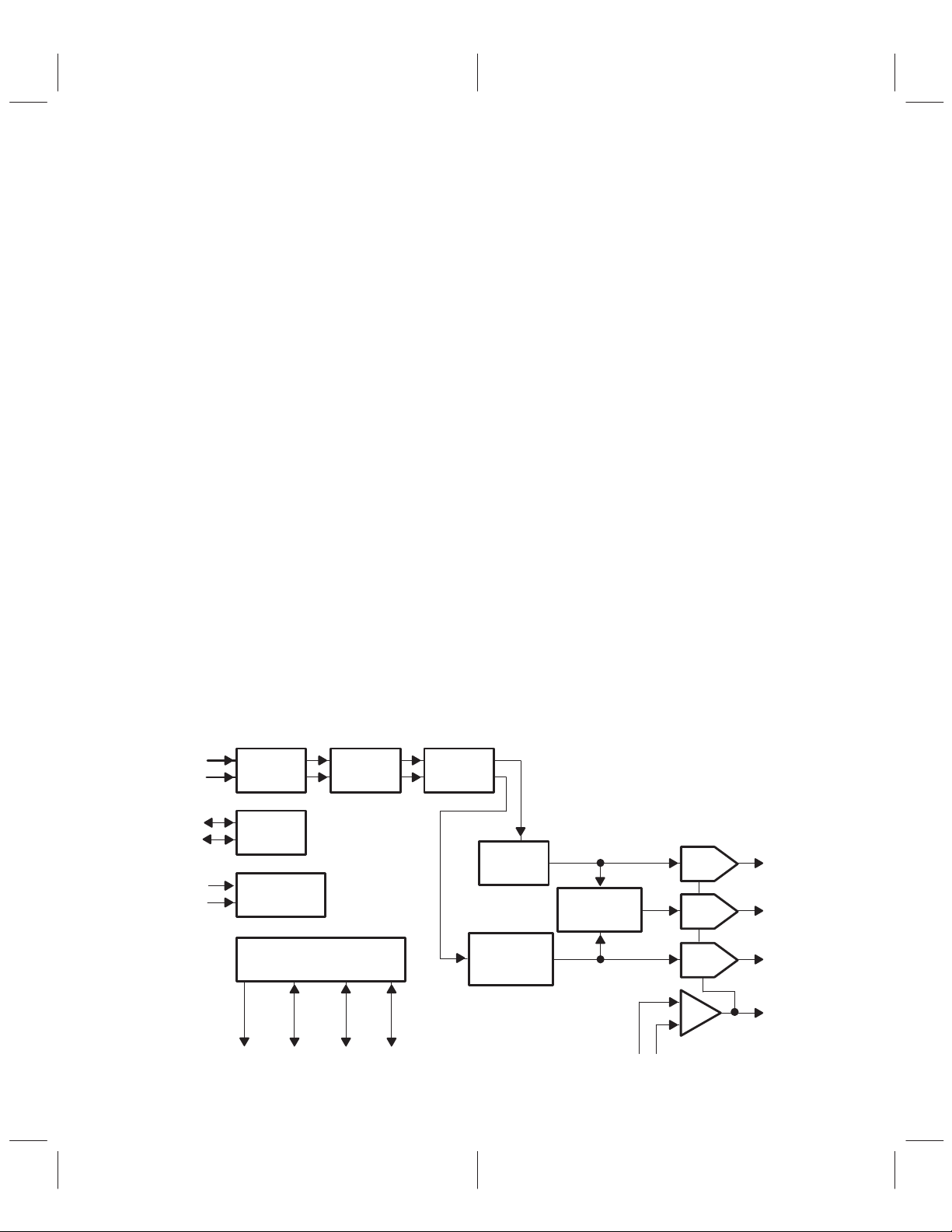
1.3 Functional Block Diagram
VP1(0–7)
VP2(0–7)
SDA
SCL
XTAL1
XTAL2
1–2
Data
Manager
Serial
Interface
Clock
Generation
RCM1
Scaling Filter
Timing and
Synchronization
RCM2
RCV1 RCV2
Closed
Caption
Modulator
and Gain
Control
Cross Color
Reduction
REF
Y
CVBS
C
COMP
FSADJ
Page 9

1.4 Terminal Assignments
PFP PACKAGE
(TOP VIEW)
DD
NC
NC
NC
XDAC
CCIR
NTSQ
PASQ
DVDD
VP1[7]
DGND
VP1[6]
VP1[5]
DGND
VP1[4]
DVDD
VP1[3]
VP1[2]
VP1[1]
VP1[0]
NC
VP2[0]
VP2[1]
59 58 57 56 5560 54
61
62
63
64
65
66
67
68
69
70
71
72
73
74
75
76
77
78
79
80
23
1
VP2[2]
VP2[3]
5678
4
VP2[4]
VP2[5]
VP2[6]
VP2[7]
52 51 5053
9
VSUB
DVDD
49 48
10 11 12 13
DGND
DVDD
47 46 45 44
14 15 16 17
INVGND
REFV
REFGND
FSADJ
DREF
43 42 41
18 19 20
COMP
VREF
40
39
38
37
36
35
34
33
32
31
30
29
27
27
26
25
24
23
22
21
NC
AVDD
CVBS
AGND
AVDD
Y
AGND
AVDD
C
AGND
NC
NC
NC
NC
NC
NC
NC
NC
NC
NC
RCV1
RCM1
RCV2
RCM2
CREF
DGND
LLC
RES
DVDD
GLCI DGND
SDEN
TST
Figure 1–1. Terminal Assignments
XT AL1
XT AL2
SA
SCL
SDA
CDIR
DGND
DVDD
1–3
Page 10
1.5 Ordering Information
I/O
DESCRIPTION
Device TVP6000CPFP
PFP: Plastic Flat Pack With Power Pad
1.6 Terminal Functions
TERMINAL
NAME NO.
AGND 31,34,37 Analog ground
AVDD 33,36,39 Analog power supply
C 32 O Chrominance analog output signal for S-video output
External clock source select. CCIR can be programmed to select different external
CCIR 65 O
CDIR 18 I
COMP 41 I/O
CREF 5 I/O Clock reference signal
CVBS 38 O Composite video output signal
DGND
DREF 43 I/O T est pin. For normal applications no connect.
DVDD
FSADJ 44 I/O
GLCI 10 I Genlock control input. GLCI is used for communicating with TVP5xxx decoder series.
INVGND 47 INVGND should be connected to AGND for normal applications.
LLC 7 I/O
NC
NTSQ 66 O
PASQ 67 O
6,19,48,
51,70,73
8,20,49,
52,68,75
21–30,40,
61–63,80
clock sources. When CCIR = 1, the encoder is set to CCIR601 mode. For detailed
programming information, refer to Table 2–11.
Clock direction input. When CDIR = 0, LLC and CREF are outputs. When CDIR = 1, LLC
and CREF are inputs.
Compensation pin for the internal reference amplifier. A 0.1-µF capacitor should be
connected between COMP and A VDD.
Digital ground
Digital power supply
Full scale adjust control. A 264-Ω resistor should be connected between FSADJ and
AGND to control the full-scale output current on the analog outputs.
Line locked clock. One of the 24.54 MHz, 27.00 MHz, or 29.5 MHz clocks for different
standards and pixel rates.
No connect
External clock source select. NTSQ can be programmed to select different external
clock sources. When NTSQ = 1, the encoder is set to NTSC square pixel mode. For
detailed programming information, refer to Table 2–11.
External clock source select. PASQ can be programmed to select different external
clock sources. When PASQ = 1, the encoder is set to PAL square pixel mode. For
detailed programming information, refer to Table 2–11.
1–4
Page 11

1.6 Terminal Functions (Continued)
I/O
DESCRIPTION
TERMINAL
NAME NO.
RCM1 1 O
RCM2 3 I/O
RCV1 2 I/O
RCV2 4 I/O
VREF 42 I/O
REFGND 45 Reference ground of output DACs. REFGND should be connected to AGND.
REFV
DD
RES 9 I Reset input, active low
SA 15 I I2C slave address select
SCL 16 I/O I2C serial clock input. Maximum clock rate of 400 kHz.
SDA 17 I/O I2C serial data line
SDEN 11 I Test pin. For normal applications connect to DGND.
TST 12 I T est pin. For normal applications connect to DGND.
VP1[7:0]
VP2[7:0] 53–60 I
VSUB 50 VSUB should be connected to AGND.
XDAC 64 I
XTAL1 13 I Crystal or oscillator input. CMOS input levels
XTAL2 14 I Crystal input. Crystal is connected between XTAL1 and XTAL2.
Y 35 O Luminance analog output signal for S-video output
46 Reference power supply of the DACs. REFVDD should be connected to AVDD.
69,71,72,
74,76–79
Programmable video vertical timing signal. For detailed programming information,
see the RCM_L21 register definition.
Programmable video horizontal timing signal (can also be programmed for horizontal
active video signal. For detailed programming information, see RCM_L21 register
definition.
Programmable video vertical timing signal. For programming infromation, see
SYN_CTRL0 register definition.
Programmable video horizontal timing signal (can also be programmed for horizontal
active video signal). For detailed programming infromation, see SYN_CTRL0
register definition.
Test pin. VREF can be used for bandgap voltage output. For normal operation no
connection.
Y input port in 16-bit mode. For 8-bit multiplexed mode, VP1[7:0] is either the YUV
I
multiplexed port or should be left unconnected based on the FMT(2) register bit.
UV input port in 16-bit mode. For 8-bit multiplexed mode, VP2[7:0] is either the YUV
multiplexed port or should be left unconnected based on the FMT(2) register bit.
XDAC sets the initial mode of operation for the output DACs immediately after reset. If
XDAC = GND the DACs will be in normal operation mode after reset. If XDAC = VDD,
the DACs will be in power down mode.
1–5
Page 12

1–6
Page 13

2 Detailed Description
The TVP6000 is a digital video encoder designed for systems requiring high-quality display of computer
graphics, video, video conferencing, and Internet content. It is designed to convert a digital video input data
stream into NTSC or P AL composite video output. Digital input formats include 8 or 16 bit YUV 4:2:2 or 8
bit CCIR–656 YUV. Analog output formats are NTSC and PAL.
The encoder provides picture quality enhancement features such as overscan compensation, which allows
up to a 12.5% down scaling of pixels (horizontal) and lines (vertical) to allow fitting a VGA frame on a NTSC.
A 3-tap antiflicker filter greatly reduces annoying flicker associated with displaying progressive scan
graphics data or text on an interlace display , like TV. The output has simultaneous S-video and composite
baseband video (CVBS) via three 10-bit DACs. Programmable features such as blank levels, color burst
amplitude, luminance and chrominance gains, subcarrier frequency, luminance delay allow for easy
optimization of picture quality and subcarrier genlock capability when used with a compatible video decoder
provides accurate color reproduction even with nonstandard or unstable video sources such as a VCR.
See Figure 2–1 for an overview of the major functional blocks of the TVP6000.
2.1 Initialization
Upon power up, the TVP6000 is initialized by the internal logic to display a color bar. With this feature, the
TVP6000 is able to demonstrate basic functionality while using only a 27-MHz clock signal at the LLC pin
or the XTAL1 and XTAL2 crystal pins. No software programming is required for this initial operation. This
serves as a quick diagnostic tool during the initial debug of a system.
The DACs can also be optionally turned off immediately after reset by connecting the XDAC pin (pin 64) to
if the initial color bar display is not desired. In this case, video is not output after reset. See Section 2.1 1,
V
DD
Register Descriptions
for details about the default values immediately after power up.
2–1
Page 14
Y
35
DAC
10-Bit
Filter
Reduction
Cross Color
CVBS
38
10-Bit
+
DAC
C
32
10-Bit
COMP
41
DAC
42 44
VREF FSADJ
sin
Closed
Caption
Generator
Scaling
Processor
+
and
Filters
LowPass
Interpolation
Y
Y
Y
76–79
69,71,72,74
Y
(5.7 MHz)
Data
Manager
Modulator
and
LowPass
UV
Unit
Cr/Cb
53–60
and
Gain Control
Filters
(1.3 MHz)
Interpolation
Cr/Cb
Cr/Cb
cos
sin
16
SCL
L.U.T.
SIN/COS
Generator
Sync. Clock
Logic
I2C Control
17
SDA
2–2
Figure 2–1. Block Diagram
Page 15
2.2 I2C Interface
The I2C interface is used to access the internal registers of the TVP6000 encoder. This two pin interface
consists of one clock line, SCL, and one serial data line, SDA. The basic I2C access cycles are shown in
Figure 2–3.
SDA
SCL
Start Condition (S) Stop Condition (P)
Figure 2–2. I2C Start and Stop Conditions
The basic access cycle consists of the following:
1. A start condition
2. A slave address cycle
3. A subaddress cycle
4. Any number of data cycles
5. A stop condition
The start and stop conditions are shown in Figure 2–2. The high-to-low transition of SDA while SCL is high,
defines the start condition. The low-to-high transition of SDA while SCL is high, defines the stop condition.
Each cycle, data or address, consists of 8 bits of serial data followed by one acknowledge bit generated by
the receiving device. Thus, each data/address cycle contains nine bits as shown in Figure 2–3.
123456789123456789123456789
SCL
SDA
MSB
Slave Address Subaddress Data
Acknowledge Acknowledge Acknowledge
Stop
Figure 2–3. I2C Access Cycles
2
As indicated in Figure 2–3, following a start condition, each I
C device decodes the slave address. The
TVP6000 responds with an acknowledge by pulling the SDA line low during the ninth clock cycle, if it
decodes the address as its address. During subsequent subaddress and data cycles, the TVP6000
responds with an acknowledge as shown in Figure 2–3. The subaddress is auto-incremented after each
data cycle.
The transmitting device must not drive the SDA signal during the acknowledge cycle so that the receiving
device may drive the SDA signal low. The not acknowledge, A
, condition is indicated by the master by
keeping the SDA signal high just before it asserts the stop, P, condition. This sequence terminates a read
cycle as shown in Figure 2–5.
2–3
Page 16
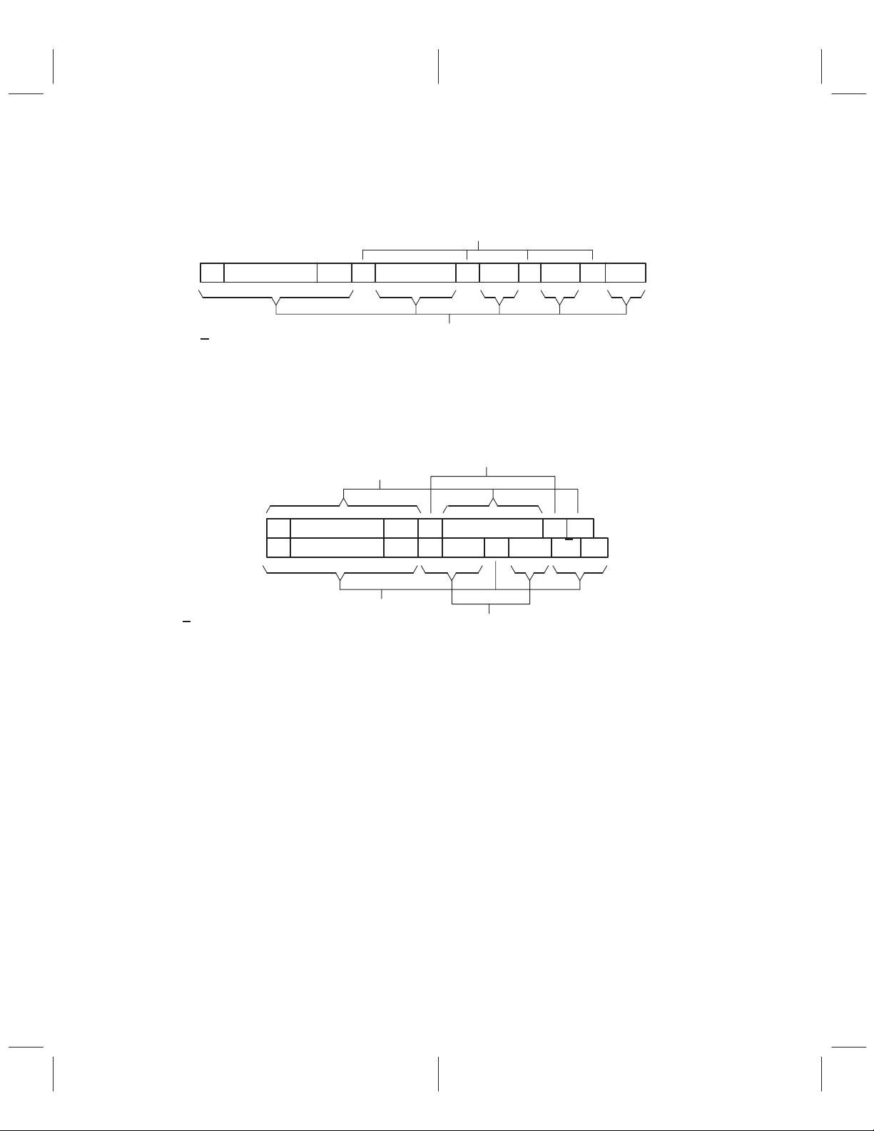
The slave address consists of 7 bits of address along with 1 bit of read/write information as shown in
Figures 2–4 and 2–5. For the TVP6000, the possible slave addresses (including the read/write bit) are 0x40
or 0x42 for write cycles or 0x41 and 0x43. Refer to Table 2–7 for additional base address information.
From Receiver
S Slave Address W Sub Address A Data A PA Data A
= No Acknowledge (SDA High)
A
A = Acknowledge
S = Start Condition
P = Stop Condition
W = Write
S Slave Address W A PA
S Slave Address R A PA Data A Data
A = No Acknowledge (SDA High)
A = Acknowledge
S = Start Condition
P = Stop Condition
W = Write
R = Read
From Transmitter
Figure 2–4. I2C Write Cycle
Receiver
Transmitter
Sub Address
Transmitter
Receiver
Figure 2–5. I2C Read Cycle
2.3 Data Manager
The data manager resides at the very beginning of the processing pipeline. It receives the Y Cb Cr pixel data
from the pixel bus and converts it to its internal YUV representation. Register F_CONTROL at subaddress
3A and the SCN bit of the SCM register at subaddress 90 define the function of the data manager.
The data manager can receive data on either an 8-bit or 16-bit video port. In the 8-bit format, it receives data
at port VP1 or VP2 (both 8-bits wide) depending on register bit FMT2, at every rising edge of LLC if scan
conversion is disabled, and at every (rising and falling) edge of LLC if scan conversion is enabled. In the
16-bit format, it receives luminance information on the VP1 port and chrominance information on the VP2
port, at alternate rising edges of LLC (qualified by CREF) if scan conversion is disabled, or at every rising
edge of LLC if scan conversion is enabled. Additionally , the data manager can generate pixels internally for
a 100/100 color bar if the CBAR bit is set. The Y, U, and V values for this color bar are shown in T able 2–3.
2–4
Page 17
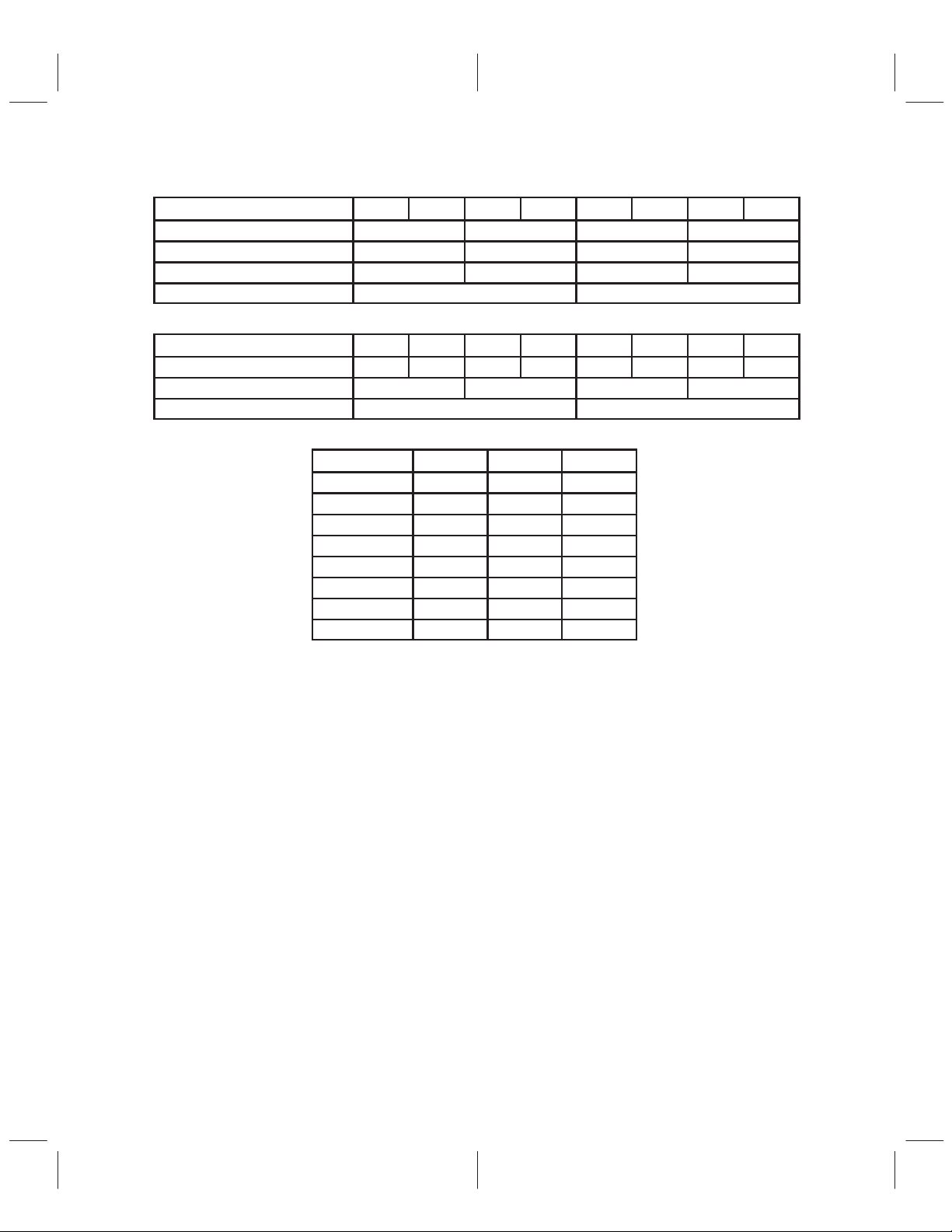
Table 2–1. 16-Bit Video Port YUV 4:2:2
TIME 0 1 2 3 4 5 6 7
VP1[7:0] Y0 Y1 Y2 Y3
VP2[7:0] Cb0 Cb1 Cb2 Cb3
Luma pixel number 0 1 2 3
Chroma pixel number 0 2
Table 2–2. 8-Bit Multiplexed Video Port CCIR656 YUV 4:2:2
TIME 0 1 2 3 4 5 6 7
VP1[7:0] or VP2[7:0] Cb0 Y0 Cr0 Y1 Cb2 Y2 Cr2 Y3
Luma pixel number 0 1 2 3
Chroma pixel number 0 2
Table 2–3. 100/100 Color Bar in Twos Complement
COLOR Y (hex) Cb (hex) Cr (hex)
White 6B 00 00
Yellow 52 90 12
Cyan 2A 26 90
Green 11 B6 A2
Magenta EA 4A 5E
Red D1 DA 70
Blue A9 70 EE
Black 90 00 00
The SCN bit in the SCM register enables or disables scan conversion. When scan conversion is disabled
(SCN = 0), the input scan lines are interlaced at a field rate of 60 Hz for 525-line systems or 50 Hz for 625-line
systems. When scan conversion is enabled (SCN = 1), the input scan lines are non-interlaced at a frame
rate of 60 Hz or 50 Hz.
2.4 Scaling Processor
The scaling processor scales down the input image in both horizontal and vertical directions. In addition to
scaling, the scaling processor filters the image in the vertical direction and removes annoying flickers, which
are common when a computer-generated graphics or text, especially a static image, is displayed on TV . The
scaling processor uses a 3-tap adaptive filter, whose coef ficients are dynamically adjusted on a line-by-line
basis to maintain optimal performance.
The scaling processor is enabled by setting the SCN register bit to 1. When scan conversion is enabled,
the data manager receives non-interlaced pixel data via the demand mode interface and passes pixel data
on to the scaling processor for overscan-compensation processing. The output of the scaling processor
feeds the video encoder core for encoding. See Section 2.5,
Video Encoder
When the scaling processor is disabled, SCN reset to 0, the data manager receives pixel data via master
or slave mode and passes pixel data directly to the video encoder core, bypassing the scaling processor.
The scaling processor, when enabled, is controlled by the following registers: SPPL, DPPL, SLPF, and
DLPF . These registers define the size of the image before and after scaling. The SPPL register defines the
number of active pixels per line before scaling and the DPPL register defines the number of active pixels
per line after scaling. The SLPF register defines the number of active lines before scaling and the DLPF
register defines the number of active lines after scaling. Refer to Section 2.11,
additional information on these registers.
for a detailed description.
Register Descriptions
for
2–5
Page 18

Vertical and horizontal over-scan compensation ratios are independently controlled by two pairs of registers.
The VDTAH and VDTAL register pair define the vertical scaling ratio and the HDTAH and HDTAL register
pair define the horizontal scaling ratio. The scaling ratio equations are given in the register description
section. An over-scan compensation ratio up to 12.5% in both vertical and horizontal directions is supported.
When enabled, three modes of vertical scaling and two modes of horizontal scaling are provided for optimal
performance of the target application. For computer graphics and text intensive static images, mode 2
vertical scaling (VSC[1:0] = 2) should be used for maximum flicker reduction. For DVD playback, mode 3
(VSC[1:0] =3) should be used for sharpness. The nearest neighbor mode is provided only for comparison
and diagnostic purposes, and should not be used for normal applications.
Finally, the scaled image can be placed on the TV screen at a location defined by the VOFS and HOFS
registers. VOFS and HOFS define the location of the upper left corner of the output image. See the
definitions of the VOFS and HOFS registers for details.
Note that the SWPF bit is provided for test and diagnostic purposes. For normal applications, this bit must
be set to 0 at all times.
2.5 Video Encoder
2.5.1 Luminance Encoding
Programmable gain is first applied to the luminance data output from the data manger or scaling processor
depending on whether the TVP6000 is in regular or scan-conversion mode. The luminance gain is defined
by the GAIN_Y register at subaddresses 5F and 60. The horizontal sync, vertical sync, and setup insertion
are then performed. Both black level and blank level are programmable through the BLACK_LEVEL and
BLANK_LEVEL registers at subaddresses 5D and 5E, respectively.
All of the transition edges of the luminance signal such as the sync edges and active video edges are
properly shaped and filtered to limit the bandwidth within the standards.
2.5.2 Luminance Low-Pass and Interpolation Filter
After all of the necessary components of the luminance signal have been added, the resultant signal is
low-passed and interpolated to a 2x pixel rate. This 2x interpolation simplifies the external analog
reconstruction filter design and improves the signal-to-noise ratio. Refer to Figure 2–6 for the filter frequency
response.
2–6
Page 19

0.5
0
–0.5
–1
–1.5
G – Gain – dB
–2
–2.5
–3
0123456
0
–5
–10
–15
–20
G – Gain – dB
–25
–30
–35
NTSC_SQP
PAL_SQP
PAL_CCIR/NTSC_CCIR
78910
f – Frequency – MHz
Figure 2–6. Luma Path Frequency Response
NTSC_CCIR
NTSC_SQP
PAL_SQP
PAL_CCIR
–40
012 3 456
f – Frequency – MHz
Figure 2–7. Luma Cross Color Reduction Filter
78 910
2–7
Page 20

2.5.3 Cross Color Reduction Filter
An optional cross color reduction filter can be applied to the luminance signal before the luminance signal
combines with the chrominance signal to form the composite signal. The cross color reduction filter reduces
the interference between the luminance and chrominance in the composite signal. The cross reduction filter
does not apply to S-video.
2.5.4 Chrominance Encoding
The time-multiplexed U/V signal is adjusted by a pair of programmable gains. The gain for U and the gain
for V are independently controlled by the GAIN_U and GAIN_V register bits respectively at subaddresses
5B, 5C, 5D, and 5E. The gain-adjusted signal then passes through a chrominance low-pass filter to limit the
bandwidth of the U/V signal. The chrominance low-pass filter can be optionally bypassed by setting the CBW
bit of the M_CONTROL register at subaddress 61 to 0. This setting enlarges the bandwidth on U/V for
S-video output.
The low-passed U/V signal is then subjected to a 1-to-4 interpolation through an interpolation filter. The data
rate for both U and V is now at a 2x pixel rate.
The U and V signals are then quadrature-modulated by the internally generated subcarrier signal to form
the chrominance (C) signal. The subcarrier reference signal color burst is inserted right before the active
video.
The frequency, the phase of the modulating subcarrier, and the amplitude of the color burst are all
programmable. When genlock is disabled (the GLCE bit of the M_CONTROL register set to 0), the
subcarrier frequency is controlled by the S_CARR registers at subaddresses 63, 64, 65, and 66. The values
of the registers are computed based on the desired subcarrier frequency and the LLC clock using the
equation in the register description. T able 2–12 lists the most commonly used values for various standards.
When genlock is enabled (GLCE set to 1), the subcarrier frequency is updated once every scan line using
the frequency control bits serially shifted in at the GLCI pin.
The C_PHASE register at subaddress 5A controls the phase of the subcarrier. The phase of the color
subcarrier is reset to C_PHASE when enabled. Four modes of color subcarrier reset are provided: reset
every two lines, every two fields, every eight fields, or at a reset bit input at the GLCI pin if genlock is enabled.
Users can use the C_PHASE register to adjust the subcarrier-to-horizontal sync phase. The bits BSTAP[6:0]
of the BSTAMP register at subaddress 62 sets the amplitude of the color burst. The PAL bit of the
M_CONTROL register enables phase alternation line encoding. A sweeping subcarrier is generated to
encode the chrominance signal when the P AL bit is set to 1. Otherwise a normal subcarrier is generated.
Phase alternation line refers to an encoding scheme in which the subcarrier alternates between two different
phases every scan line. There are two possible alternate sequences and the PALPHS bit of the
M_CONTROL register selects one of the sequences.
2–8
Page 21

0
NTSC_SQP
–10
–20
–30
G – Gain – dB
–40
–50
–60
0 0.5 1 1.5 2 2.5 3
f – Frequency – MHz
PAL_SQP
PAL_CCIR/NTSC_CCIR
3.5 4 4.5 5
Figure 2–8. Chroma Path Frequency Response
2.6 Closed Caption
The TVP6000 can be programmed to encode closed caption data and extended data in the selected line.
The closed caption data are sent to the TVP6000 through the I
seven-bit US-ASCII code and one odd parity bit as shown below.
MSB
odd-parity bit6 bit5 bit4 bit3 bit2 bit1 bit0
Closed caption data format
US-ASCII LSB
The standard service encodes closed caption only in the odd field, while the extended service encodes
closed caption in both fields. L21ENA, when set to 1, enables closed caption encoding in the odd field and
L21ENB, when set to 1 enables closed caption encoding in the even field.
The scan line where closed caption is to be encoded is programmable through the SLINE register at
subaddress 6B.
Four closed caption data registers contain the closed caption data to be encoded. Registers LINE21_O0
and LINE21_O1 contain the first byte and the second byte of the close caption data to be encoded in the
odd field. Registers LINE21_E0 and LINE21_E1 contain the first byte and the second byte of the closed
caption data to be encoded in the even field. Immediately after the closed caption data is written to the closed
caption data registers either for the odd field or even field, the corresponding closed caption status bit, CCE
or CCO in the STA TUS register at subaddress 02, is reset to 0 to indicate the closed caption data is available
in the closed caption data registers and yet to be encoded. Immediately after the closed caption is encoded,
the CCE or CCO bit is set to 1 to indicate the closed caption data has been encoded and is ready to accept
new data. The null character is automatically inserted if the closed caption data is not written to the closed
caption data registers in time for encoding.
The run-in clock frequency is 503496.5 Hz ( 32 × fline of NTSC ). The closed caption data is encoded in the
format of non-return to zero (NRZ). Additionally , the data translates to the IRE scale in the following manner:
0= 0 IRE; 1 = 50 IRE.
2
C interface. The data stream consists of a
2–9
Page 22
The following four figures present the parameters of a closed caption line implemented in different
standards.
59.65 µS
2 Null Characters
10 µS
27.4 µS
(7 Cycles)
13.9 µS
Transition
Time: 220 ns
Figure 2–9. NTSC CCIR601 Rate Closed Caption Line
59.67 µS
2 Null Characters
10 µS
27.4 µS
(7 Cycles)
13.9 µS
Transition
Time: 240 ns
2–10
Figure 2–10. P AL CCIR601 Pixel Rate Closed Caption Line
Page 23

59.67 µS
2 Null Characters
27.4 µS
10 µS
(7 Cycles)
13.9 µS
Figure 2–11. NTSC Square Pixel Rate Closed Caption Line
61.2 µS
2 Null Characters
27.5 µS
10.2 µS
(7 Cycles)
13.9 µS
Transition
Time: 200 ns
Transition
Time: 200 ns
Figure 2–12. P AL Square Pixel Rate Closed Caption Line
2.7 Clock Generation
When the CDIR pin is tied low, the TVP6000 generates the clock from the crystal connected between XTAL1
and XT AL2. Optionally , an oscillator connected to XT AL1 can also be used. The clock is used internally and
is also properly buffered and output at the LLC pin. The clock qualifying reference signal, CREF, is also an
output in this mode.
When CDIR is tied high, the LLC and CREF pins are inputs. The TVP6000 receives the clock signal from
the LLC pin and the clock qualifying reference signal from the CREF pin.
2.8 Analog Output
The TVP6000 supports simultaneous composite and S-video outputs. Additionally, the DACs may be
independently turned off via software to minimize power dissipation.
The output DACs are current sources and are optimal for driving a 37.5-Ω load with double 75-Ω termination.
A 264-Ω full-scale adjust resistor must be connected between the FSADJ pin and ground.
2–11
Page 24

For cost-sensitive consumer applications, passive low-pass filters are recommended. Figure 2–13
illustrates the termination of the output DACs. An external analog filter, as shown in the figure, is also
required.
1 µH 2.7 µH 0.7 µH
TVP6000
CVBS/Y/C
To 75-Ω Cable
75 Ω
470 pF 330 pF 56 pF
Figure 2–13. Output Filter
2.9 Video Port Interface
The TVP6000 provides a highly flexible video port interface, which users can tailor to fit their target
applications. The video port interface consists of four raster controls: RCV1, RCV2, RCM1, and RCM2, an
8-bit or 16-bit pixel port: VP1 and/or VP2, and two clock related signals: LLC and CREF.
2.9.1 RCV1
When scan conversion is disabled (SCN reset to 0), RCV1 can be programmed as an input or an output.
When RCV1 is used as an input, RCV1 can be programmed to receive vertical sync, frame sync, or
sequence sync. At the same time, RCV1 can optionally be selected as the source of horizontal sync. The
TVP6000 maintains three counters internally; horizontal counter, vertical counter , and field counter in order
to generate correct timing for encoding. The horizontal sync input re-triggers the horizontal counter by
resetting the horizontal counter to a preset value defined by the HTRIGGER0 and HTRIGGER1 registers.
Similarly , the vertical sync input re-triggers the vertical counter by resetting the vertical counter to a preset
value defined by the VTRIGGER0 and VTRIGGER1 registers. The frame sync input forces the field to be
the odd field. The sequence sync resets the field to be the first field of the field sequence.
When RCV1 is used as an output, RCV1 can be programmed to generate either vertical sync, frame sync,
or sequence sync.
When scan-conversion is enabled (SCN =1), the demand mode video port interface is activated and RCV
is output only and operates as the new frame indicator.
The polarity of RCV1 is programmable. Refer to the description of the SYN_CTRL0 register for details.
2.9.2 RCV2
When scan conversion is disabled, the RCV2 pin can be programmed as an input or an output.
When RCV2 is used as an input, RCV2 can be used as the horizontal sync based on the HSINSEL bit of
the SYN_CTRL0 register. RCV2 is used as the blanking signal if the CBLFV2 bit of the SYN_CTRL0 register
is set to 1, regardless whether or not RCV2 has been selected as the horizontal sync.
When scan-conversion is enabled, the demand mode video port interface is activated and RCV2 is output
only and operates as the new line indicator.
Similar to RCV1, the polarity of RCV2 is programmable. Refer to the description of the SYN_CTRL0 register
for details.
2.9.3 RCM1
RCM1 is always an output. This pin may be programmed to output either vertical sync, frame sync, or
sequence sync. Unlike RCV1 and RCV2, the polarity of RCM1 is not programmable. Refer to the description
of the RCM_L21 register for details.
2–12
Page 25

2.9.4 RCM2
The RCM2 pin may be configured as an input or an output as shown in T able 2–19. The polarity of the RCM2
pin is programmable via this register as well.
As an output, this pin may be operated as a horizontal sync, composite blank, or a demand mode data
request signal. As in input, this pin is always a composite blanking input.
When scan-conversion is enabled, the demand mode video port interface is activated and the RCM2 pin
acts as the request output pin.
2.10 Modes of Operation
With a highly programmable video port interface, the TVP6000 may be configured to operate in various
modes, each tailored for a target application. In the following sections, several of the most commonly used
modes are described.
2.10.1 Master Mode
In the master mode, the TVP6000 generates all of the video timing signals for controlling an external
graphics controller or MPEG decoder device. Table 2–4 lists the timing signals that are output from the
TVP6000 during master mode.
T able 2–4. Master Mode
PIN NAME I/O TYPE DESCRIPTION
LLC Input/output Line locked clock; with 2X pixel clock frequency.
CREF Input/output Data phase reference clock.
RCM1 Output Output vertical/field timing, can be programmed as VSO/FSO/FSEQO
RCV1 Output Output vertical/field timing, can be programmed as VSO/FSO/FSEQO
RCM2 Output
RCV2 Output
Output horizontal timing, programmed as CBNO. Active duration is defined
by registers BMRQ and EMRQ, excluding vertical blanking interval.
Output horizontal timing, programmed as HSO. Active duration is defined
by registers BRCV and ERCV.
Refer to Table 2–15 and Table 2–17 for the definitions of VSO, FSO, FSEQO, and HSO.
A crystal with the correct frequency according to Table 2–5 should be connected between pins XTAL1 and
XT AL2.
T able 2–5. Crystal Frequencies
PIXEL RATE CLOCK FREQUENCY
CCIR-601 27 MHz 27 MHz
Square pixel 24.5454 MHz 29.5 MHz
2.10.2 Slave Mode
In slave mode, all clock and video timing signals are supplied from an external source. The source may be
a graphics controller, an MPEG device, or a TV decoder such as the TVP5010/TVP5020 decoders.
Table 2–6 lists the signal definitions for slave mode.
2–13
Page 26
T able 2–6. Slave Mode Signals
PIN NAME I/O TYPE DESCRIPTION
LLC Input
CREF Input
RCM1 Output
RCV1 Input
RCM2 Input
RCV2 Input
Line locked clock with 2X pixel clock frequency. CDIR pin is tied high.
Data phase reference clock. CDIR pin is tied high.
Output Vertical/Field timing, can be programmed as VSO/FSO/FSEQO
Can be programmed as VSI/FSI/FSEQI.
Programmed as CBNI.
Programmed as HSI.
Refer to T able 2–15 and Table 2–17 for the definition of VSO, FSO, FSEQO, HSO, VSI, FSI, FSEQI, CBNI,
and HSI.
2.10.3 Demand Mode
Demand mode is an interface specially designed for scan conversion. When scan conversion is enabled,
the TVP6000 accepts non-interlaced pixel data, performs signal processing functions which include
non-interlace-to-interlace conversion, flicker filtering and overscan-compensation, and outputs interlaced
NTSC/PAL video. Due to the nature of the functions that the TVP6000 performs during scan conversion,
the bandwidth of the input pixel increases and exceeds what the master and slave mode interface can
provide. Demand mode provides extra bandwidth to meet the needs of the TVP6000.
Unlike master mode and slave mode, the video port interface timing for demand mode is decoupled from
the timing of the internal encoder core.
The TVP6000 operates in demand mode when it requests data from an external graphics controller or an
MPEG device. Demand mode is enabled by setting SCM[0] = 1, the SCN bit.
In demand mode, the TVP6000 asserts the RCM2 pin high to request additional data from the external
source and negates the RCM2 pin to stop additional data transfer. Table 2–19 shows how the RCM2 pin
may be programmed to operate as a request signal during demand mode. In addition, the NLR register is
used to program the threshold where the RCM2 pin is toggled for requests.
2.10.4 Genlock Mode
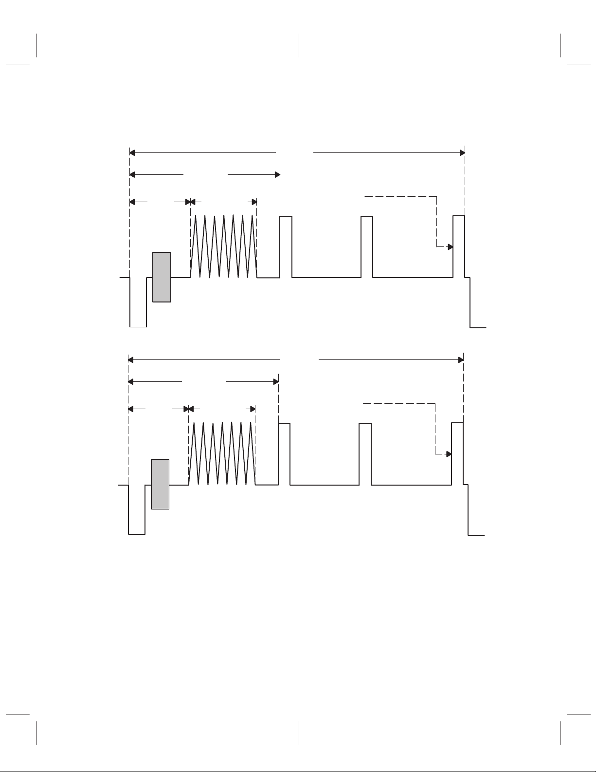
The TVP6000 may be configured in a genlock mode to an external TV decoder such as the
TVP5000/TVP5010 device. This configuration allows the decoder to drive video timing information to the
TVP6000 encoder. The genlock mode is used to control clock jitter and thus allows the encoder to generate
accurate color burst information.
In this configuration, GLCI pin is connected to the GLCO pin of the decoder, and the line-lock clock pin, LLC,
is fed by the decoder main pixel clock output. Moreover, the color sub-carrier information is formatted as
a 23-bit binary number and is transmitted serially . The transmission timing diagram is shown in Figure 2–13.
2–14
Page 27

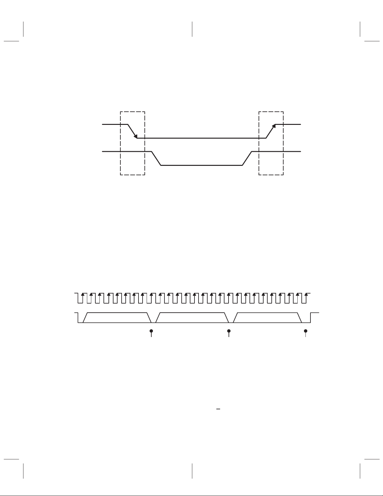
SCLK
GLCO
Inactive
>128 LLCs
Start Bit 0
MSB LSB
23-Bit DTO Frequency Control
1 LLC 23 LLCs
Where DTO = Discrete Time Oscillator
Inactive
7 LLCs
Sub Carrier DTO Phase Reset
1 LLC
Figure 2–14. Transmission Timing
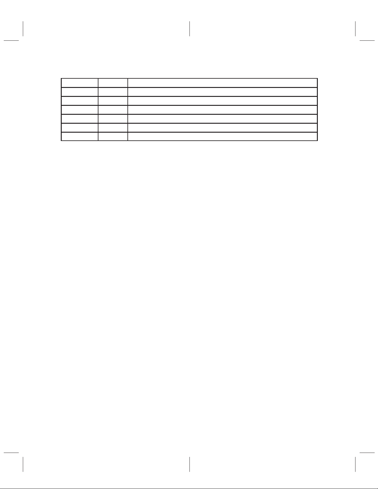
2.11 Register Descriptions
The TVP6000 is a standard I2C slave device. All of the registers can be written and read through the I2C
interface. The I2C base addresses of the TVP6000 are dependent on pin 15 (SA) as listed in Table 2–7.
T able 2–7. Base Addresses
PIN 15 WRITE ADDRESS
0 40 41
1 42 43
(hex)
T able 2–8. Register Bit Allocation Map
REGISTER R/W
DEV_ID R 00 Dev id[7:0]
REV_ID R 01 Rev id[7:0]
STATUS R 02 Scon Ccon Cce Cco Fsq[2:0]
Reserved 03–39 Reserved
F_CONTROL R/W 3A Cbar Fmt2 Y2c Uv2c Fmt[1:0]
Reserved 3B–59 Reserved
C_PHASE R/W 5A Cphase[7:0]
GAIN_U R/W 5B Gu[7:0]
GAIN_V R/W 5C Gv[7:0]
BLACK_LEVEL R/W 5D Gu8 Black[6:0]
BLANK_LEVEL R/W 5E Gv8 Blank[6:0]
GAIN_Y R/W 5F Gy[7:0]
X_COLOR R/W 60 0 Xc Gy8 Lcd[2:0]
M_CONTROL R/W 61 Sdown Cdown Palphs 0 Glce Cbw Pal Ffrq
BSTAMP R/W 62 Sqp Bstap[6:0]
S_CARR1 R/W 63 Fsc[7:0]
S_CARR2 R/W 64 Fsc[15:8]
S_CARR3 R/W 65 Fsc[23:16]
S_CARR4 R/W 66 Fsc[31:24]
LINE21_O0 R/W 67 L21o[7:0]
LINE21_O1 R/W 68 L21o[15:8]
SUB-
ADDRESS
BIT7 BIT6 BIT5 BIT4 BIT3 BIT2 BIT1 BIT0
READ ADDRESS (hex)
2–15
Page 28
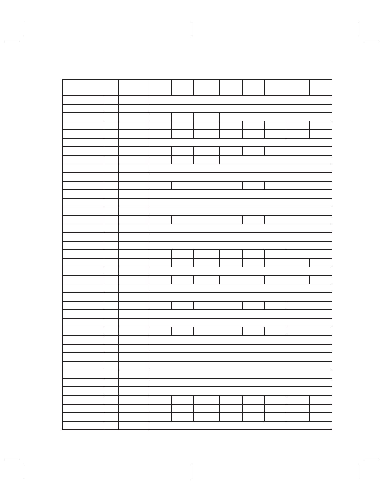
T able 2–8. Register Bit Allocation Map (Continued)
REGISTER R/W
LINE21_E0 R/W 69 L21e[7:0]
LINE21_E1 R/W 6A L21e[15:0]
LN_SEL R/W 6B Sline[4:0]
SYN_CTRL0 R/W 6C Rcv1a Rcv1b Hsinel Orcv1 Prcv1 Cblfv2 Orcv2 Prcv2
RCML21 R/W 6D Crcm2 Cblfm2 Orcm2 Prcm2 Rcm1a Rcm1b L21ena L21enb
HTRIGGER0 R/W 6E htrig[7:0]
HTRIGGER1 R/W 6F Htrig[10:8]
VTRIGGER R/W 70 Presa Presb Sblank Vtrig[4:0]
BMRQ R/W 71 Bmrq[7:0]
EMRQ R/W 72 Emrq[7:0]
BEMRQ R/W 73 Emrq[10:8] Bmrq[10:8]
RESERVED 74–76 Reserved
BRCV R/W 77 Brcv[7:0]
ERCV R/W 78 Ercv[7:0]
BERCV R/W 79 Ercv[10:8] Brcv[10:8]
FLEN R/W 7A Flen[7:0]
FAL R/W 7B Fal[7:0]
LAL R/W 7C Lal[7:0]
FLAL R/W 7D Lal8 Fal8 Flen[9:8]
SYN_CTRL1 R/W 7E Esav Ignp Free Blnks Avm[1:0]
RESERVED 7F Reserved
SCM R/W 90 Swpf Hsc[1:0] Vsc[1:0] Scn
SLPF R/W 91 Slpf[7:0]
SPPL R/W 92 Sppl[7:0]
SLPH R/W 93 Sppl[9:8] Slpf[9:8]
DLPF R/W 94 Dlpf[7:0]
DPPL R/W 95 Dppl[7:0]
DLPH R/W 96 Dppl[9:8] Dlpf[9:8]
VDTAL R/W 97 Vdta[7:0]
VDTAH R/W 98 Vdta[15:8]
HDTAL R/W 99 Hdta[7:0]
HDTAH R/W 9A Hdta[15:8]
VOFS R/W 9B Vofs[7:0]
HOFS R/W 9C Hofs[7:0]
NLR R/W 9D Nlr[7:0]
TEST1 R/W 9E
TEST2 R/W 9F
TEST3 R/W A0
RESERVED A1–FF Reserved
SUB-
ADDRESS
BIT7 BIT6 BIT5 BIT4 BIT3 BIT2 BIT1 BIT0
2–16
Page 29

2.11.1 DEV_ID
Subaddress:00 (Read Only) Default: 0x60
7 6 5 4 3 2 1 0
Dev_ID[7:0]
This read only register contains the device ID for the TVP6000. The 8-bit device ID for the TVP6000 is 0x60.
2.11.2 REV_ID
Subaddress:01 (Read Only) Default: 0x00
7 6 5 4 3 2 1 8
Rev_ID[7:0]
This read only register contains the revision ID for the TVP6000. The revision ID identifies different revisions
of the device.
2.11.3 STATUS
Subaddress:02 (Read Only)
7 6 5 4 3 2 1 0
SCON CCON CCE CCO FSQ[2:0]
Where:
SCON S-video connection status
0 Not connected
1 Connected
CCON Composite video connection status
0 Not connected
1 Connected
CCE Closed-caption status bit for even field. This bit is set immediately after the data in
registers LINE21_E0 and LINE21_E1 has been encoded to closed caption. This bit is
reset when both of these registers are written.
CCO Closed-caption status bit for odd field. This bit is set immediately after the data in
registers LINE21_O0 and LINE21_O1 has been encoded to closed caption. This bit is
reset when both of these registers are written.
FSQ[2:0] Field sequence ID. For P AL, all three bits FSQ[2:0] are used whereas for NTSC only
bits FSQ[1:0] are meaningful. Futhermore, FSQ(0) represents the odd field when it is a
0 and the even field when it is 1.
2–17
Page 30
2.11.4 F_CONTROL
Subaddress:3A Default: 0x8D
7 6 5 4 3 2 1 0
CBAR FTM[2] Y2C UV2C FTM[1:0]
Format control register. This register specifies the input video source and format.
Where:
CBAR Select video data source
0 Use external video source
1 Use internal color bars
Y2C Y data format selection
0 The input Y data are in twos complement format
1 The input Y data are in binary format
UV2C CrCb data format selection
0 The input CrCb data is in twos complement format
1 The inputCrCb data is in binary format
FTM[2:0] These three bits detemine the video input data stream format and timing as listed
in Table 2–9. The SCN bit (subaddress 90, bit 0) is also used in this decode.
T able 2–9. Input Format and Data Sampling
INTERNAL
SCN FTM[2:0] INPUT FORMAT SAMPLING TIME
0 X 0 0 Reserved Reserved Reserved
0 X 0 1 YUV 4:2:2 on VP1 and VP2
0 0 1 0 YUV 4:2:2 on VP1 port Data is sampled at the rising edge of LLC LLC
0 1 1 0 YUV 4:2:2 on VP2 port Data is sampled at the rising edge of LLC LLC
0 0 1 1 CCIR 656 on VP1 port Data is sampled at the rising edge of LLC LLC
0 1 1 1 CCIR 656 on VP2 port Data is sampled at the rising edge of LLC LLC
1 X 0 0 Reserved Reserved Reserved
1 X 0 1 YUV 4:2:2 Data is sampled at the rising edge of LLC LLC
1 0 1 0 YUV 4:2:2 on VP1 port Data is sampled at both edges of LLC LLC
1 1 1 0 YUV 4:2:2 on VP2 port Data is sampled at both edges of LLC LLC
1 X 1 1 Reserved
Data is sampled at the rising edge of LLC
qualified by CREF.
ENCODER
LLC
CLOCK
2–18
Page 31

2.11.5 C_PHASE
Subaddress: 5A Default: 0x00
7 6 5 4 3 2 1 0
CPHS[7:0]
Where:
CPHS[7:0] Phase of encoded video color subcarrier (including the color burst) relative to
Hsync. The adjustable step is 360/256.
2.11.6 GAIN_U
Subaddress: 5B Default: 0x01
7 6 5 4 3 2 1 0
GU[7:0]
Where:
GU[7:0] Gain control of Cb signal. The MSB, GU8, is located at subaddress 5D, bit 7.
In the case of NTSC with a 7.5 IRE pedestal, WHITE – BLACK = 92.5 IRE
Gain_U= 0x101.
In the case of no pedestal (PAL/SECAM), WHITE – BLACK = 100 IRE.
Gain_U = 0x115.
2.11.7 GAIN_V
Subaddress: 5C Default: 0x6B
7 6 5 4 3 2 1 0
GV[7:0]
Where:
GV[7:0] Gain control of Cr signal. The MSB, GV8 is located at subaddress 5E, bit 7.
In the case of NTSC with a 7.5 IRE pedestal, WHITE – BLACK = 92.5 IRE.
Gain_V = 0x16B.
In the case of no pedestal (PAL/SECAM), WHITE – BLACK = 100 IRE.
Gain_V = 0x18C.
2.11.8 BLACK_LEVEL
Subaddress: 5D Default: 0xCC
7 6 5 4 3 2 1 0
GU8 BLACK[6:0]
Where:
GU8 The most significant bit of the GAIN_U register. See the GAIN_U register for more
information.
BLACK[6:0]Black level setting for NTSC = 0x4C and for PAL = 0x3C.
2–19
Page 32

2.11.9 BLANK_LEVEL
Subaddress: 5E Default: 0xB8
7 6 5 4 3 2 1 0
GV8 BLANK[6:0]
Where:
GV8 The most significant bit of the GAIN_V register. See the GAIN_V register for more
information.
BLANK[6:0]Blank level setting for NTSC = 0x38 and for PAL = 0x3C.
2.11.10 GAIN_Y
Subaddress: 5F Default: 0x2E
7 6 5 4 3 2 1 0
GY(7–0)
Where:
GY[7:0] Gain control of Y signal. The MSB, bit 8, is located at subaddress 60, bit 5.
In the case of NTSC with a 7.5 IRE pedestal, WHITE – BLACK = 92.5 IRE.
Gain_Y = 0x12E
In the case of no pedestal (PAL/SECAM), WHITE – BLACK = 100 IRE.
Gain_Y = 0x145
2.11.11 X_COLOR
Subaddress: 60 Default: 0x20
7 6 5 4 3 2 1 0
XC GY8 LCD(2–0)
Cross color and chroma delay compensation register
Where:
XC Cross color reduction enable for composite video output. Cross color does not affect
S-video output
0 Cross color reduction is disabled (default)
1 Cross color reduction is enabled
GY8 MSB of Gain_Y register.
LCD[2:0] These three bits can be used for chroma channel delay compensation during S-video
mode. Table 2–10 shows the delay corresponding to the LCD[2:0] settings.
T able 2–10. Chroma Channel Delays
LCD[2:0]
0 0 0 0
0 0 1 0.5 pixel clock period
0 1 0 1 pixel clock period
0 1 1 1.5 pixel clock period
1 x x 2 pixel clock period
2–20
DELAY ON CHROMA
CHANNEL
Page 33

2.11.12 M_CONTROL
Subaddress: 61 Default: 0x05
7 6 5 4 3 2 1 0
SDOWN CDOWN PALPHS GLCE CBW PAL FFRQ
Mode control register. This register provides various operating mode controls including DAC power
management.
Where:
SDOWN S-video DAC power down
0 Normal operation (default)
1 Power down mode
CDOWN Composite video DAC power down
0 Normal operation (default)
1 Power down mode
P ALPHS PAL switch phase setting
0 PAL switch phase is nominal (default)
1 PAL switch phase is inverted compared to nominal
GLCE Genlock control enable. See Table 2–20.
0 No genlock to the color subcarrier frequency (default)
1 Genlock-to-color subcarrier frequency is from the TVP5010
CBW Chrominance encoding bandwidth enlarge enable
0 Bandwidth for chrominance encoding is enlarged
1 Standard bandwidth for chrominance encoding (default)
P AL Phase alternation line encoding selection
0 Phase alternation line encoding disabled (default)
1 Phase alternation line encoding enabled
FFRQ Field rate selection. Refer to Table 2–11 for programming information.
0 50 Hz
1 60 Hz (default)
2.11.13 BSTAMP
Subaddress: 62 Default:0x38
7 6 5 4 3 2 1 0
SQP BSTAP[6:0]
Color burst amplitude
Where:
SQP Square-pixel sampling rate. Refer to Table 2–11 for programming information.
0 CCIR601 sampling rate
1 Square-pixel sampling rate
BSTAP[6:0]Setting of the amplitude of color burst. The value for NTSC = 0x38 and for
P AL = 0x41.
The SQP and FFRQ bits control the total number of horizontal pixels displayed per scan line. In addition,
these bits control the CCIR, NTSQ, and PASQ status pins as shown in Table 2–11.
2–21
Page 34

T able 2–11. Total Horizontal Pixel Selection
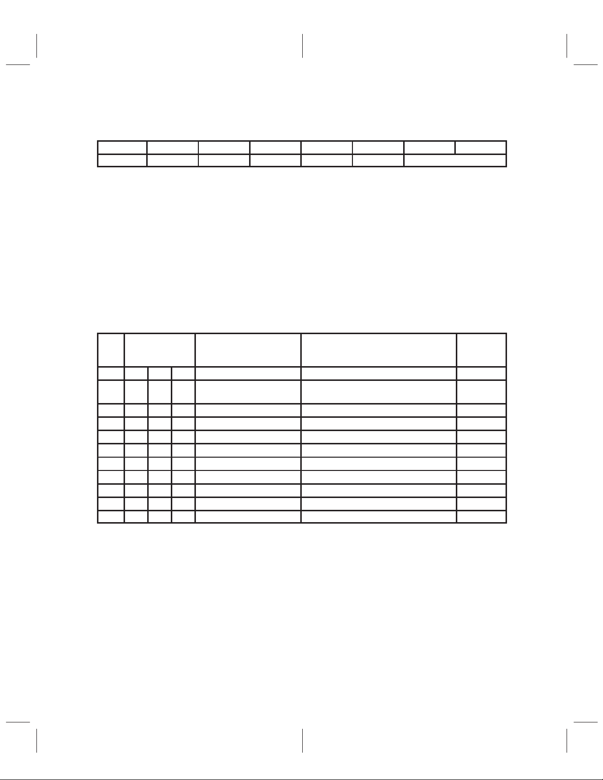
MODE SQP FFRQ CCIR NTSQ PASQ NUMBER OF PIXELS PER LINE
CCIR601 PAL 0 0 high low low 864
CCIR601 NTSC 0 1 high low low 858
Square pixel PAL 1 0 low low high 944
Square pixel NTSC 1 1 low high low 780
2.11.14 S_CARR1, 2, 3, 4
Subaddress: 63, 64, 65, 66 Default: 0xF6, 0x7B, 0xF0, 0x21
7 6 5 4 3 2 1 0
FSC07 FSC06 FSC05 FSC04 FSC03 FSC02 FSC01 FSC00
FSC15 FSC14 FSC13 FSC12 FSC11 FSC10 FSC09 FSC08
FSC23 FSC22 FSC21 FSC20 FSC19 FSC18 FSC17 FSC16
FSC31 FSC30 FSC29 FSC28 FSC27 FSC26 FSC25 FSC24
Color subcarrier frequency registers
Where:
FSC[31:0] These four bytes of data are used to program the color subcarrier frequency . These
four bytes are determined by the following formula.
32
S_carr = ROUND((Fsc/Fclock) × 2
Table 2–12 lists some common values for S_CARR.
T able 2–12. S_CARR Values
STANDARD
M/NTSC Rectangular 3.579545 MHz 27 MHz 569408543 (default) 21F07C1F
B, D, G, H, I, N/PAL Rectangular 4.43361875 MHz 27 MHz 705268427 2A098ACB
N/PAL
(combination N/PAL)
M/PAL Rectangular 3.5756083125 MHz 27 MHz 568782819 21E6EFE3
M/NTSC Square 3.579545 MHz 24.5454 MHz 626349397 25555555
B, D, G, H, I, N/PAL Square 4.43361875 MHz 29.5 MHz 645499916 26798C0C
N/PAL
(combination N/PAL)
Combinational N Square 3.5756083125 MHz 24.5454 MHz 625661 101 254AD4AD
PIXEL
TYPE
Rectangular 3.58205625 MHz 27 MHz 569807942 21F69446
Square 3.58205625 MHz 29.5 MHz 521519134 1F15C01E
SUBCARRIER
FREQUENCY (fsc)
)
CLOCK
(fclock)
S_CARR (dec) S_CARR (hex)
2–22
Page 35

2.11.15 LINE21_O0
Subaddress: 67
7 6 5 4 3 2 1 0
L21O[7:0]
Where:
L21O[7:0] Least significant byte of of closed caption data in odd field.
Initial value is undefined.
2.11.16 LINE21_O1
Subaddress: 68
7 6 5 4 3 2 1 0
L21O[15:8]
Where:
L21O[15:8] Most significant byte of closed caption data in odd field.
Initial value is undefined.
2.11.17 LINE21_E0
Subaddress: 69
7 6 5 4 3 2 1 0
L21E[7:0]
Where:
L21E[7:0] Least significant byte of extended service data in even field.
2.11.18 LINE21_E1
Subaddress: 6A
7 6 5 4 3 2 1 0
L21E[15:8]
Where:
L21E[15:08] Most significant byte of extended service data in even field.
2.11.19 LN_SEL
Subaddress: 6B
7 6 5 4 3 2 1 0
SLINE[4:0]
Where:
SLINE[4:0] Selects the line where closed caption or extended service data are encoded.
2–23
Page 36

2.11.20 SYN_CTRL0
Subaddress: 6C Default: 0x00
7 6 5 4 3 2 1 0
RCV1A RCV1B HINSEL ORCV1 PRCV1 CBLFV2 ORCV2 PRCV2
This register provides I/O control and the functional definition for the RCV1 and RCV2 pins.
Where:
RCV1A This bit along with the RCV1B, SCN (bit 0, subaddress 90) define the signal type on
pin RCV1. See Table 2–13 and Table 2–14.
RCV1B This bit along with the RCV1A, SCN (bit 0, subaddress 90) define the signal type on
pin RCV1. See Table 2–13 and Table 2–14.
HSINSEL Horizontal synchronization input selection
0 RCV1 pin is the Hsync input
1 RCV2 pin is the Hsync input
ORCV1 Output RCV1
0 RCV1 is set as an input pin
1 RCV1 is set as an output pin
PRCV1 Polarity setting of RCV1
0 RCV1 is active high when it is set as an output, the rising edge is the
active edge when it is set as an input.
1 RCV1 is active low when it is set as an output, the falling edge is the
active edge when it is set as an input.
CBLFV2 Composite blanking output on RCV2. This bit combined with the SCN bit (bit 0,
subaddress 90), CBLFV2 (bit 2, subaddress 6C), and HSINSEL bits (bit 5,
subaddress 6C) define the signal type on RCV2. See Table 2–16 for
programming information.
ORCV2 Output RCV2
0 RCV2 is set as an input pin
1 RCV2 is set as an output pin
PRCV2 Polarity setting of RCV2
0 RCV2 polarity is active high. The rising edge of RCV2 is the active edge.
1 RCV2 polarity is active low. The falling edge of RCV2 is the active edge.
2–24
Page 37

The RCV1 pin configurations are listed in Table 2–13.
SCN
RCV1A
RCV1B
HSINSEL
Table 2–13. RCV1 Pin Configurations
RCV1 PIN
AS OUTPUT AS INPUT
0 0 0 0 VSO Unused
0 0 0 1 VSO VSI
0 0 1 0 FSO HSI and FSI
0 0 1 1 FSO FSI
0 1 0 0 FSEQO HSI and FSEQI
0 1 0 1 FSEQO FSEQI
0 1 1 X Reserved Reserved
1 X X X NFO Reserved
The RCV1 symbols and signal descriptions are listed in Table 2–14.
T able 2–14. RCV1 Symbols and Signal Descriptions
SYMBOL SIGNAL DESCRIPTION
VSO Field synchronization output. Active once every field during vertical sync period. For NTSC, VS = 3 lines,
VSI Vertical synchronization input. Retriggers the vertical counter . The active edge in the first half of the scan
FSO Frame synchronization output. Active in the odd field (first field). Inactive in the even field (second field).
FSEQO Field sequence. For NTSC (bit 0, subaddress 61 set to 1), active only in the first field of every four fields. For
NFO New frame indicator output. In scan conversion mode (SCN set to 1), the active edge of this signal
HSO Horizontal synchronization output.
HSI Horizontal synchronization input. Retriggers the horizontal counter.
FSI Frame synchronization input. Retriggers the vertical counter and resets the field to odd.
FSEQI Field sequence input. Retriggers the vertical counter and resets the field to the first of four fields for NTSC
for PAL, VS = 2.5 lines.
line resets the vertical counter to VTRIG.
PAL (bit 0, subaddress 61 reset to 0), active only in the first field of every eight fields.
indicates to external logic to advance to the next frame.
or the first of eight fields for PAL.
The RCV2 pin configurations are listed in Table 2–15.
Table 2–15. RCV2 Pin Configurations
SCN CBLFV2 HSINSEL
0 0 0 HSO No function
0 0 1 HSO HSI
0 1 0 CBNO CBNI
0 1 1 CBNO HSI and CBNI
1 X X NLO Reserved
RCV2 PIN
AS OUTPUT AS INPUT
2–25
Page 38

The RCV2 symbols and signal descriptions are listed in Table 2–16.
T able 2–16. RCV2 Symbols and Signal Descriptions
SYMBOL SIGNAL DESCRIPTION
HSO Horizontal synchronization output. As an output, RCV2 is asserted between BRCV and ERCV in every line
HSI As an input, RCV2 is used for horizontal synchronization. Retriggers the horizontal counter.
CBNO As an output, RCV2 is asserted between BRCV and ERCV from line FAL to LAL excluding VBI.
CBNI As an input, RCV2 is used for composite blanking.
NLO Output only , RCV2 generates a 4 LLC clock wide new line indicator at the beginning of a line to indicate to
including VBI.
the external logic to advance to the next line.
2.11.21 RCM_L21
Subadress: 6D Deault: 0x00
7 6 5 4 3 2 1 0
CRCM2 CBLFM2 ORCM2 PRCM2 RCM1A RCM1B L21ENA L21ENB
Where:
CRCM2 CREF modulation enable
0 CREF modulation is disabled
1 CREF modulation is enabled
When RCM2 is programmed as an active video output (ORCM2 = 1), CREF
modulation is enabled (CRCM2 = 1), and a 16-bit video input port is used, RCM2
is modulated by the internal CREF signal. The modulation is performed
before polarity control.
CBLFM2 See Table 2–18 for programming information.
ORCM2 I/O setting of RCM2
0 RCM2 is set as an input pin (default).
1 RCM2 is set as an output pin.
PRCM2 Polarity setting of RCM2
0 RCM2 polarity is active high (default).
1 RCM2 polarity is active low.
RCM1A Determines which signal is output to pin RCM1. Refer to Table 2–17.
RCM1B Determines which signal is output to pin RCM1. Refer to Table 2–17.
L21ENA This bit controls the extended service closed caption encoding. See T able 2–19 for
progamming information.
L21ENB This bit controls the closed caption encoding. See Table 2–19 for
progamming information.
2–26
Page 39

Table 2–17. RCM1 Output Signals
SCN
CBLFM2
CBLFV2
HSINSEL
SIGNAL DESCRIPTION
RCM1A RCM1B PIN RCM1 DESCRIPTION
0 0 VS Vertical synchronization (default)
0 1 FS Frame synchronization
1 0 FSEQ Field sequence. For NTSC, FSEQ is high in the first field of every four fields.
1 1 N/A Reserved
For PAL, FSEQ is high in the first field of every eight fields.
T able 2–18 shows the operating modes of pin RCM2 as defined by the SCN (bit 0, subaddress 98), CBLFM2
(bit 6, subaddress 6D), CBLFV2 (bit 2, subaddress 6C), and HSINSEL bits (bit 5, subaddress 6C).
Table 2–18. RCM2 Pin Configurations
RCM2 PIN
AS OUTPUT AS INPUT
0 0 X X HSO No function As an output, RCM2 is asserted between
0 1 0 0 CBNO No function As an output, RCM2 is asserted between
0 1 0 1 CBNO CBNI As an input, RCM2 is used for composite
0 1 1 X CBNO No function As an output, RCM2 is asserted between
1 X X X RQO Reserved As an output only. RCM2 is used as
BMRQ and EMRQ in every line including
VBI (sub-address 71–73)
BMRQ and EMRQ in every line excluding
VBI.
blanking. As an output, RCM2 is asserted
between BMRQ and EMRQ in every line
excluding VBI.
BMRQ and EMRQ in every line excluding
VBI.
request for pixels. When asserted, this
signal sources the pixel on the bus at the
clock edge and informs external logic to
output next pixel.
T able 2–19. Encoding Setting
L21ENA L21ENB LINE 21 ENCODING MODE
0 0 Line 21 encoding off
0 1 Enables encoding in first field (odd field)
1 0 Enables encoding in second field (even field)
1 1 Enables encoding both fields
2–27
Page 40

2.11.22 HTRIGGER0
Subaddress: 6E Default: 0xE0
7 6 5 4 3 2 1 0
HTRIG[7:0]
Where:
HTRIG[7:0] Least significant bit of horizontal trigger phase setting for RCV1 and RCV2 as inputs.
HTRIG is expressed in half-pixels or clk2x periods.
2.11.23 HTRIGGER1
Subaddress: 6F Default: 0x8C
7 6 5 4 3 2 1 0
HTRIG[10:8]
Where:
HTRIG[10:8] Most significant bit of horizontal trigger phase setting for RCV1 and RCV2 as
inputs. HTRIG is expressed in half-pixels or clk2x periods.
2.11.24 VTRIGGER
Subaddress: 70 Default: 0xC0
7 6 5 4 3 2 1 0
PRESA PRESB SBLANK VTRIG[4:0]
Where:
PRESA Phase reset A. Used as shown in Table 2–20.
PRESB Phase reset B. Used as shown in T able 2–20. These two bits decide how frequently
the color subcarrier is reset to CPHS (subaddress 5A). GLCE is bit 3, subaddress 61.
SBLANK Vertical blanking setting
0 Vertical blanking is defined by the settings of the FAL and LAL registers
1 Vertical blanking is forced automatically during field synchronization and
equalization.
VTRIG[4:0] Vertical trigger reference for pin RCV1. These bits specify where on a field of sixteen
lines the RCV1 pin is triggered. The VTRIG field is expressed in units of a half line.
T able 2–20. Phase Reset Modes
GLCE PRESA PRESB PHASE RESET MODE
0 0 0 No reset
0 0 1 Reset every two lines
0 1 0 Reset every eight fields
0 1 1 Reset every four fields
1 X X Reset by reset bit on GLCI pin
2–28
Page 41

2.11.25 BMRQ
Subaddress: 71
7 6 5 4 3 2 1 0
BMRQ[7:0]
Beginning of master request.
Where:
BMRQ[7:0] These bits define the starting pixel position on a horizontal display line where active
video will be displayed. The upper three bits, BMRQ[10:8], reside in register
BEMRQ, subaddress 73. These settings shape the RCM2 pin output.
2.11.26 EMRQ
Subaddress: 72
7 6 5 4 3 2 1 0
EMRQ[7:0]
End of master request.
Where:
EMRQ[7:0] These bits define the ending pixel position on a horizontal display line where active
video will end. The upper three bits, EMRQ[10:8], reside in register BEMRQ,
subaddress 73. These settings shape the RCM2 pin output.
2.11.27 BEMRQ
Subaddress: 73
15 14 13 12 11 10 9 8
EMRQ[10:8] BMRQ[10:8]
Overflow register for master request.
Where:
EMRQ[10:8] Upper three bits of register EMRQ. See EMRQ register definition
BMRQ[10:8] Upper three bits of register BMRQ. See BMRQ register definition
2.11.28 BRCV
Subaddress: 77
7 6 5 4 3 2 1 0
BRCV[7:0]
Beginning of raster control, RCV2, out.
Where:
BRCV[7:0] These bits along with the CBLFV2 bit in the SYN_CTRL0 register defines the
beginning of the active output at pin RCV2. The upper three bits of this register are in
register BERCV, subaddress 79.
2–29
Page 42
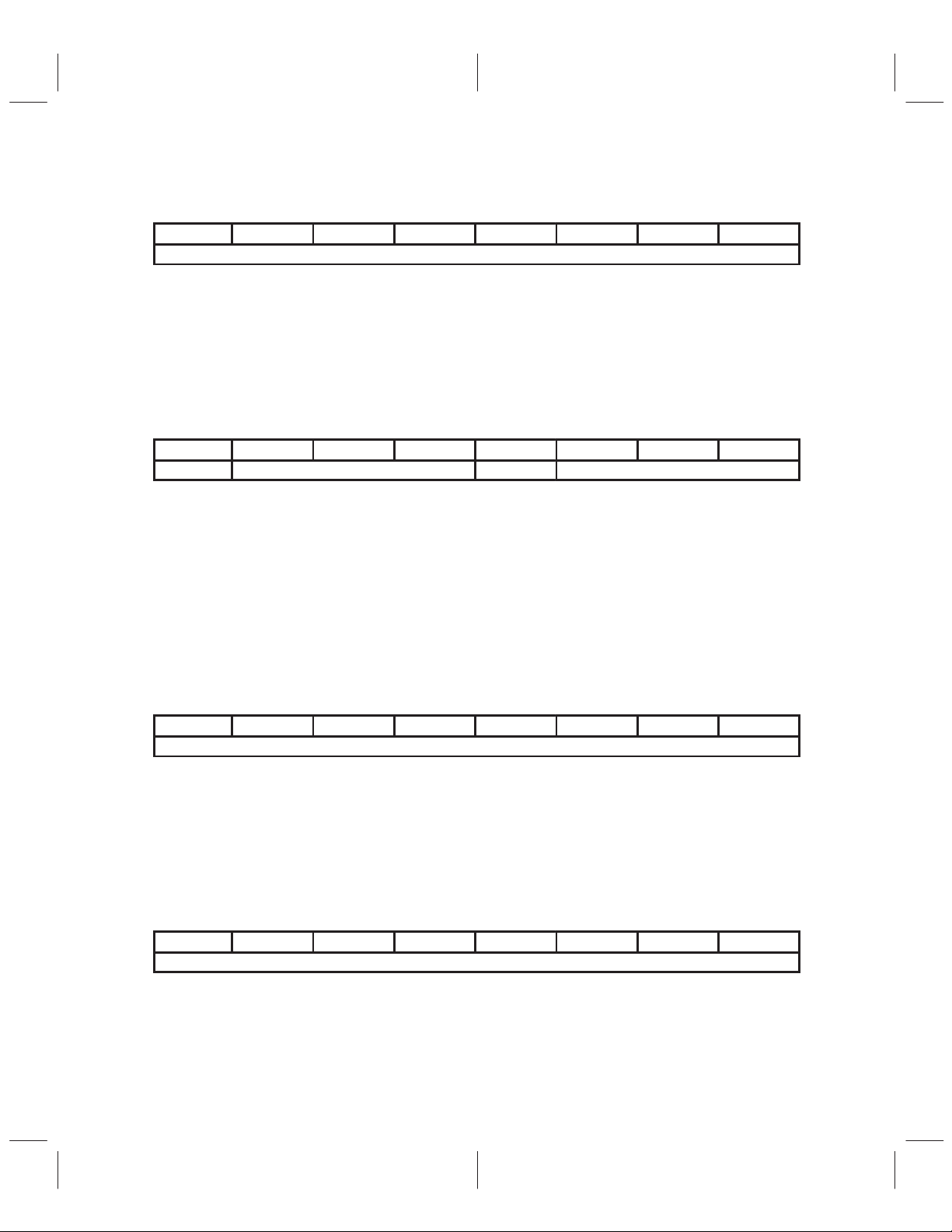
2.11.29 ERCV
Subaddress: 78
7 6 5 4 3 2 1 0
ERCV[7:0]
End of raster control, RCV2, out.
Where:
ERCV[7:0] These bits along with the CBLFV2 bit in the SYN_CTRL0 register defines the ending
of the active output at pin RCV2. The upper three bits of this register are in register
BERCV, subaddress 79.
2.11.30 BERCV
Subaddress: 79
15 14 13 12 11 10 9 8
ERCV[10:8] BRCV[10:8]
Overflow register for BRCV and ERCV fields.
Where:
ERCV[10:8]These bits along with the CBLFV2 bit in the SYN_CTRL0 register define the ending
of the active output at pin RCV2. The lower eight bits of this register are in register
ERCV, subaddress 78.
BRCV[10:8]These bits along with the CBLFV2 bit in the SYN_CTRL0 register define the
beginning of the active output at pin RCV2. The lower eight bits of this register are in
register BRCV, subaddress 77.
2.11.31 FLEN
Subaddress: 7A Default: 0x0C
7 6 5 4 3 2 1 0
FLEN[7:0]
Field length
Where:
FLEN[7:0] These bits define the number of half lines in each field. The upper two bits of this
register arer located in the FLAL register.
Length of field = (FLEN + 1) half lines
2.11.32 FAL
Subaddress: 7B Default: 0x12
7 6 5 4 3 2 1 0
FAL[7:0]
First active line of a field
Where:
FAL[7:0] These bits define the first active line of a field. The MSB is located in the FLAL
register.
2–30
Page 43

2.11.33 LAL
Subaddress: 7C Default:0x03
7 6 5 4 3 2 1 0
LAL[7:0]
Last active line of a field.
Where:
LAL[7:0] These bits define last active line of a field. The MSB is located in the register FLAL.
2.11.34 FLAL
Subaddress: 7D Default: 0x22
7 6 5 4 3 2 1 0
LAL[8] FAL[8] FLEN[9:8]
First and last active line of a field. Overflow bits from FAL and LAL registers.
Where:
LAL[8] These bits define the last active line of a field. The LSB is located in the LAL register.
FAL[8] These bits define the first active line of a field. The LSB is located in the FAL register .
FLEN[9:8] These bits define the number of half lines in each field. The lower eight bits of this
register are located in the FLEN register.
2.11.35 SYN_CTRL1
Subaddress: 7E Default: 0x18
7 6 5 4 3 2 1 0
ESAV IGNP FREE BLNKS AVM[1:0] FID
Where:
ESAV Enable for the detection of F and V bits only on EAV in CCIR656 input mode
0 Detection of F and V bits on both EAV and SAV
1 Detection of F and V bits only on EAV
IGNP Ignore protection bits in CCIR656 input mode
0 Protection bits not ignored
1 Protection bits ignored
FREE Free running
0 Free running disabled
1 Free running enabled. All external signals are ignored. Internal timing
signals are used.
BLNKS Blank shaping
0 Blank shaping disabled
1 Blank shaping enabled
A VM[1:0] Active video mode. See Table 2–21.
2–31
Page 44

T able 2–21. Active Video Modes
AVM[1] AVM[0] ACTIVE VIDEO MODE
0 0 Active video gating signal is the combination of:
0 1 Active video gating signal is the combination of:
1 0 Active video gating signal is generated externally.
1 1 Active video gating signal is the combination of:
1. Default horizontal gating
2. Programmable vertical gating defined by FAL, LAL, and SBLANK.
3. External gating
1. Default horizontal gating
2. Programmable vertical gating defined by FAL, LAL, and SBLANK.
1. Programmable internal horizontal gating defined by BRCV and ERCV.
2. Programmable vertical gating defined by FAL, LAL, and SBLANK.
2.11.36 SCM
Subaddress: 90 Default: 0x00
7 6 5 4 3 2 1 0
SWPF HSC[1:0] VSC[1:0] SCN
Scan conversion register. This register provides control bits for overscan compensation.
Where:
SWPF SwapField. This bit must be set to 0 for normal applications
0 Fields are not swapped
1 Fields are swapped
HSC[1:0] Horizontal scaling and interpolation mode
0 0 Horizontal scaling disabled
0 1 Nearest neighbor
1 0 Interpolation filter coefficients are according to inverse square law
1 1 Reserved
VSC[1:0] Vertical scaling and interpolation filter mode
0 0 Vertical scaling disabled
0 1 Nearest neighbor
1 0 Interpolation filter coefficients = (1/4 1/2 1/4)
1 1 Interpolation filter coefficients = (1/8 3/4 1/8)
SCN Scan conversion enable
0 Noninterlaced-to-interlaced scan conversion disabled
1 Noninterlaced-to-interlaced scan conversion enabled
2.11.37 SLPF
Subaddress: 91
7 6 5 4 3 2 1 0
SLPF[7:0]
Source scan lines per frame before scaling.
Where:
SLPF[7:0] Number of lines per frame in the source image before scaling. The most significant
two bits of this field are located in the SLPH register.
2–32
Page 45
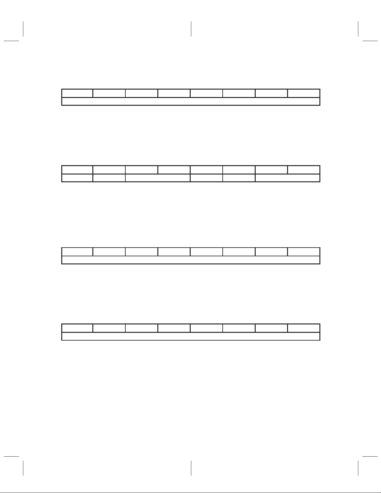
2.11.38 SPPL
Subaddress: 92
7 6 5 4 3 2 1 0
SPPL[7:0]
Source pixels per scan line before scaling.
Where:
SPPL[7:0] Number of pixels per line in the source image before scaling. SPPL0 is hardwired to
0. The most significant two bits of this field are located in the SLPH register.
2.11.39 SLPH
Subaddress: 93
7 6 5 4 3 2 1 0
SPPL[9:8] SLPF[9:8]
Where:
SPPL[9:8] Number of pixels per scan line in the source image before scaling. The LSB of this
field is located in the SPPL register.
SLPF[9:8] Number of lines per frame in the source image before scaling. The LSB of this field is
located in the SLPF register.
2.11.40 DLPF
Subaddress: 94
7 6 5 4 3 2 1 0
DLPF[7:0]
Destination lines per frame after scaling.
Where:
DLPF[7:0] Number of lines per frame in the destination image after scaling. The two most
significant bits of this field are located in the DLPH register.
2.11.41 DPPL
Subaddress: 95
7 6 5 4 3 2 1 0
DPPL[7:0]
Destination pixels per scan line.
Where:
DPPL[7:0] Number of lines per frame in the destination image after scaling. DPPL0 is hardwired
to 0. The two most significant bits of this field are located in the DLPH register.
2–33
Page 46
2.11.42 DLPH
Subaddress: 96
7 6 5 4 3 2 1 0
DPPL[9:8] DLPF[9:8]
Where:
DPPL[9:8] Number of pixels per scan line in the destination image after scaling. The LSB of this
field are located in the DPPL register.
DLPF[9:8] Number of lines per frame in the destination image after scaling. The LSB of this field
is located in the DLPF register.
2.11.43 VDTAL
Subaddress: 97
7 6 5 4 3 2 1 0
VDTA[7:0]
Where:
VDTA[7:0] Vertical over-scan compensation ratio. The MSB of this field is located in the VDT AH
register. The value of VDTA is calculated as follows:
VDTA = ROUND(((SLPF/DLPF)–1)×2^16)
where SLPF = Number of scan lines per frame in the source image before scaling,
DLPF = Number of lines per frame in the destination image after scaling.
2.11.44 VDTAH
Subaddress: 98
7 6 5 4 3 2 1 0
VDTA[15:8]
Where:
VDTA[15:8]Vertical over-scan compensation ratio. The LSB of this field is located in the VDT AL
register. Refer to the description of VDTAL for more information.
2.11.45 HDTAL
Subaddress: 99
7 6 5 4 3 2 1 0
HDTA[7:0]
Where:
HDTA[7:0] Horizontal over-scan compensation ratio. The MSB of this field is located in the
HDTAH register. The value of HDTA is calculated as follows:
HDTA = ROUND(((SPPL/DPPL)–1)×2^16 )
where SPPL = Number of pixels per line in the source image before scaling,
DPPL = Number of pixels per line in the destination image after scaling.
2–34
Page 47
2.11.46 HDTAH
Subaddress: 9A
7 6 5 4 3 2 1 0
HDTA[15:8]
Where:
HDTA[15:8] Horizontal over-scan compensation ratio. The LSB of this field is located in the
HDTAL register. Refer to the description of HDTAL for more information.
2.11.47 VOFS
Subaddress: 9B
7 6 5 4 3 2 1 0
VOFS[7:0]
Vertical of fset
Where:
VOFS[7:0] Vertical offset of the scaled image on the screen in lines from beginning of the field.
This register is used with HOFS register to position the scaled image on the screen.
Vertical of fset is given in units of two scan lines in a field or four scan lines in a
frame.
2.11.48 HOFS
Subaddress: 9C
7 6 5 4 3 2 1 0
HOFS[7:0]
Horizontal offset
Where:
HOFS[7:0] Horizontal offset of the scaled image on the screen in pixels from the beginning of the
scan line. Used with VOFS register to position the scaled image on the screen.
Horizontal offset is given in units of four pixels.
2.11.49 NLR
Subaddress: 9D
7 6 5 4 3 2 1 0
NLR[7:0]
New line request
Where:
NLR[7:0] The minimum number of LLC clock delays between the trailing edge of NEWLINE
and the leading edge of REQUEST. The value must be sufficiently large to give the
graphics controller enough time to supply pixel data when REQUEST is asserted.
2.11.50 TEST1, TEST2, TEST3
Subaddress: 9E, 9F, A0
These three register are reserved for chip test purposes only . No applications should access them.
2–35
Page 48

2–36
Page 49

3 Electrical Characteristics
3.1 Absolute Maximum Ratings Over Operating Free-Air Temperature Range
(Unless Otherwise Noted)
Digital power supply voltage range, DV
Analog power supply voltage range, AV
Digital input voltage range, V
Digital output voltage range, V
Operating free-air temperature range, T
Storage temperature range, T
Maximum total power dissipation, P
†
Stresses beyond those listed under “absolute maximum ratings” may cause permanent damage to the device. These
are stress ratings only and functional operation of the device at these or any other conditions beyond those indicated
under “recommended operating conditions” is not implied. Exposure to absolute-maximum-rated conditions for
extended periods may affect device reliability.
†
–0.5 V to 7 V. . . . . . . . . . . . . . . . . . . . . . . . . .
DD
–0.5 V to 7 V. . . . . . . . . . . . . . . . . . . . . . . . . . .
–0.5 V to 5.5 V. . . . . . . . . . . . . . . . . . . . . . . . . . . . . . . . . . . .
I
0 V to 5.5 V. . . . . . . . . . . . . . . . . . . . . . . . . . . . . . . . . . . . .
O
–65°C to 150°C. . . . . . . . . . . . . . . . . . . . . . . . . . . . . . . .
stg
DD
0°C to 70°C. . . . . . . . . . . . . . . . . . . . . . . . . . . .
A
2 W. . . . . . . . . . . . . . . . . . . . . . . . . . . . . . . . . . . . . . .
D
3.2 Recommended Operating Conditions
MIN NOM MAX UNIT
Digital supply voltage, DV
Analog supply voltage, AV
Digital low-level input voltage, V
Digital high-level input voltage, V
Digital supply current, I
Analog supply current, I
Reference voltage, V
External load resistor, double termination, R
Output load capacitance, DAC, C
Operating free-air temperature, T
DD
DD
IL
IH
DD
DD
REF
L
A
L
4.75 5 5.25 V
4.75 5 5.25 V
0 0.8 V
2.4 V
1.23 1.25 1.29 V
37.5 Ω
25 pF
0 70 °C
DD
180 mA
125 mA
V
3.3 DC Electrical Characteristics, TA = 25°C, DVDD = AVDD = 5 V
PARAMETER TEST CONDITIONS MIN TYP MAX UNIT
V
OL
V
OH
I
lkg
C
i
INL Integral nonlinearity RL = 37.5 Ω ±2 LSB
DNL Differential nonlinearity RL = 37.5 Ω ±1 LSB
I
o
Z
o
C
o
F
out
†
Maximum leakage current for XTAL1 and XTAL2 pins is 50 µA.
Low-level output voltage 0 0.4 V
High-level output voltage 2.4 V
Input leakage current 5
Input capacitance f = 1 MHz 10 pF
Resolution (each DAC) 10 bit
Output current (each DAC) RL = 37.5 Ω 34.8 38 mA
Output impedance 20 kΩ
Output capacitance f = 1 MHz 5 pF
Full scale DAC output 182.68 IRE
DD
†
V
µA
3–1
Page 50

3.4 AC Electrical Characteristics, TA = 25°C, DVDD = AVDD = 5 V
NTSC/PAL
Periods
PARAMETER TEST CONDITIONS MIN TYP MAX UNIT
DP Differential phase, video
DG Differential gain, video
SNR Signal-to-noise ratio, video 70
Luma nonlinearity 1.2 %
Subcarrier tolerance 0.0028 Hz
Analog output skew (Y to C) 1.2 ns
Y/C gain 97 %
†
SNR measured as specified in EIA/TIA–250–C.
3.5 Timing Requirements
TEST CONDITIONS MIN NOM MAX UNIT
f
I2C
f
LLC
t
su
t
hd
t
pd
t
reset
t
(NLR)
t
SPPL
Clock frequency, I2C interface 2 kΩ pull-up resistor,
Duty cycle, I2C interface 50 %
Clock frequency, pixel clock
Input data setup time, digital interface f
Input data hold time, digital interface f
Output delay time, digital interface f
Synchronize reset time 200 ns
New line request, register 0x9D
Register 0x92
400 pF
CCIR 601 27
NTSC square pixel
PAL square pixel 29.5
= 30 MHz 5 ns
LLC
= 30 MHz 2 ns
LLC
= 30 MHz 18 ns
LLC
24.5454
2 degrees
2 %
†
400 kHz
dB
MHz
3.6 Demand Mode Timing
t
d(TVIHV2L)
t
w(TV2PW)
t
d(TV2HVIL)
Delay time, RCV1 high to RCV2 low 2
Pulse duration, RCV2 4
Delay time, RCV2 high to RCV1 low 2
3.7 Switching Characteristics
t
r
t
f
3–2
Rise time, pixel clock CL= 50 pF 4 ns
Fall time, pixel clock CL = 50 pF 4 ns
Duty cycle, pixel clock 50 %
TEST CONDITIONS MIN NOM MAX UNIT
CLKX2
TEST CONDITIONS MIN NOM MAX UNIT
Page 51

CLOCK OUT
LLC
INPUT DATA
OUTPUT DATA
RCV1
RCV2
RCM2
CLOCK IN
LLC
t
hd
t
su
Valid Valid
Valid Valid
t
hd
Figure 3–1. Data Setup and Hold Timing
t
d(TVIHV2L)
t
w(TV2PW)
t
d(NLR)
t
SPPL
Figure 3–2. Demand Mode Timing
t
f
t
f
t
d(TV2HVIL)
t
r
t
r
3–3
Page 52

3–4
Page 53
Appendix A
Example Register Settings
Table A–1 lists the register settings for various NTSC and PAL applications. The following modes are
represented in the table. All of the modes except NSDM employ genlock mode. The genlock mode is
described in more detail in Section 3.
N601 NTSC standard with CCIR-601 compliant pixels and slave mode configuration
NSQP NTSC standard with square pixels and slave mode configuration
P601 PAL standard with CCIR-601 compliant pixels and slave mode configuration
PSQP PAL standard with square pixels and slave mode configuration
NSDM NTSC standard with square pixels and demand mode configuration
T able A–1. Example Register Settings
REGISTER ADDRESS N601 NSQP P601 PSQP NSDM
F_CONTROL 3A 0E 0E 0E 0E 0E
CPHS 5A 00 00 00 00 00
GAIN_U 5B 01 01 10 10 01
GAIN_V 5C 6B 6B 80 80 6B
BLACKLVL 5D CC CC BE BE CC
BLANKLVL 5E B8 B8 BE BE B8
GAIN_Y 5F 2E 2E 3F 3F 2E
XCOLOR 60 60 60 60 60 60
M_CTRL 61 05 05 06 06 05
BSTAMP 62 38 B8 3F BF B8
S_CARR0 63 1F 55 CB 0C 55
S_CARR1 64 7C 55 8A 8C 55
S_CARR2 65 F0 55 09 79 55
S_CARR3 66 21 25 2A 26 25
LINE21O0 67 94 94 94 94 94
LINE21O1 68 26 26 26 26 26
LINE21E0 69 80 80 80 80 80
LINE21E1 6A 80 80 80 80 80
LN_SEL 6B 11 11 11 11 11
SYNCTRL0 6C 12 12 12 12 12
RCML21 6D 21 21 21 21 21
HTRIG0 6E 00 00 00 00 00
HTRIG1 6F 00 00 00 00 00
VTRIG 70 C0 C0 80 80 C0
BMRQ 71 82 74 8C 9A 74
A–1
Page 54

T able A–1. Example Register Settings (Continued)
REGISTER ADDRESS N601 NSQP P601 PSQP NSDM
EMRQ 72 46 F8 4C 9A F8
BEMRQ 73 30 20 30 30 20
BRCV 77 82 74 8C 9A 74
ERCV 78 46 F8 4C 9A F8
BERCV 79 30 20 30 30 20
FLEN 7A 0C 0C 70 70 0C
FAL 7B 17 17 17 17 17
LAL 7C 02 02 34 34 02
FLAL 7D 22 22 22 22 22
SYN_CTRL1 7E 0A 0A 0A 0A 0A
SCM 90 00 00 00 00 55
SLPFL 91 00 00 00 00 E0
SPPLL 92 00 00 00 00 80
SLPH 93 00 00 00 00 21
DLPFL 94 00 00 00 00 AC
DPPLL 95 00 00 00 00 3A
DLPH 96 00 00 00 00 21
VDTAL 97 00 00 00 00 1A
VDTAH 98 00 00 00 00 1F
HDTAL 99 00 00 00 00 70
HDTAH 9A 00 00 00 00 1F
VOFS 9B 00 00 00 00 0F
HOFS 9C 00 00 00 00 09
NLR 9D 00 00 00 00 1D
A–2
Page 55

Appendix B
Mechanical Data
PFP (S-PQFP-G80) PowerPAD PLASTIC QUAD FLATPACK
0,50
0,27
0,17
0,08
M
61
80
1,05
0,95
60
41
40
Thermal Pad
(see Note D)
21
1
9,50 TYP
12,20
SQ
11,80
14,20
SQ
13,80
20
0,25
0,15
0,05
0,75
0,45
0,13 NOM
Gage Plane
0°–7°
1,20 MAX
NOTES: A. All linear dimensions are in millimeters.
B. This drawing is subject to change without notice.
C. Body dimensions include mold flash or protrusions.
D. The package thermal performance may be enhanced by bonding the thermal pad to an external thermal
plane. This pad is electrically and thermally connected to the backside of the die and possibly selected
leads.
E. Falls within JEDEC MS-026
PowerPAD is a trademark of Texas Instruments Incorporated.
Seating Plane
0,08
4146925/A 01/98
B–1
Page 56

B–2
Page 57

IMPORTANT NOTICE
T exas Instruments and its subsidiaries (TI) reserve the right to make changes to their products or to discontinue
any product or service without notice, and advise customers to obtain the latest version of relevant information
to verify, before placing orders, that information being relied on is current and complete. All products are sold
subject to the terms and conditions of sale supplied at the time of order acknowledgement, including those
pertaining to warranty, patent infringement, and limitation of liability.
TI warrants performance of its semiconductor products to the specifications applicable at the time of sale in
accordance with TI’s standard warranty. Testing and other quality control techniques are utilized to the extent
TI deems necessary to support this warranty . Specific testing of all parameters of each device is not necessarily
performed, except those mandated by government requirements.
CERT AIN APPLICATIONS USING SEMICONDUCTOR PRODUCTS MAY INVOLVE POTENTIAL RISKS OF
DEATH, PERSONAL INJURY, OR SEVERE PROPERTY OR ENVIRONMENTAL DAMAGE (“CRITICAL
APPLICATIONS”). TI SEMICONDUCTOR PRODUCTS ARE NOT DESIGNED, AUTHORIZED, OR
WARRANTED TO BE SUITABLE FOR USE IN LIFE-SUPPORT DEVICES OR SYSTEMS OR OTHER
CRITICAL APPLICA TIONS. INCLUSION OF TI PRODUCTS IN SUCH APPLICATIONS IS UNDERST OOD TO
BE FULLY AT THE CUSTOMER’S RISK.
In order to minimize risks associated with the customer’s applications, adequate design and operating
safeguards must be provided by the customer to minimize inherent or procedural hazards.
TI assumes no liability for applications assistance or customer product design. TI does not warrant or represent
that any license, either express or implied, is granted under any patent right, copyright, mask work right, or other
intellectual property right of TI covering or relating to any combination, machine, or process in which such
semiconductor products or services might be or are used. TI’s publication of information regarding any third
party’s products or services does not constitute TI’s approval, warranty or endorsement thereof.
Copyright 1998, Texas Instruments Incorporated
 Loading...