


TVP5146M2
NTSC/PAL/SECAM 4×10-Bit Digital Video Decoder
With Macrovision™ Detection, YPbPr Inputs, 5-Line Comb
Filter, and SCART Support
Data Manual
PRODUCTION DATA information is current as of publication date.
Products conform to specifications per the terms of the Texas
Instruments standard warranty. Production processing does not
necessarily include testing of all parameters.
Literature Number: SLES141F
July 2005–Revised November 2010

TVP5146M2
SLES141F–JULY 2005–REVISED NOVEMBER 2010
www.ti.com
Contents
1 Introduction ........................................................................................................................ 9
1.1 Features ...................................................................................................................... 9
1.2 Description ................................................................................................................. 10
1.3 Applications ................................................................................................................ 11
1.4 Related Products .......................................................................................................... 11
1.5 Document Conventions ................................................................................................... 11
1.6 Ordering Information ...................................................................................................... 11
1.7 Functional Block Diagram ................................................................................................ 12
1.8 Terminal Assignments .................................................................................................... 13
1.9 Terminal Functions ........................................................................................................ 14
2 Functional Description ....................................................................................................... 16
2.1 Analog Processing and A/D Converters ................................................................................ 16
2.1.1 Video Input Switch Control .................................................................................... 17
2.1.2 Analog Input Clamping ......................................................................................... 17
2.1.3 Automatic Gain Control ........................................................................................ 17
2.1.4 ADCs ............................................................................................................. 17
2.2 Digital Video Processing .................................................................................................. 17
2.2.1 2x Decimation Filter ............................................................................................ 18
2.2.2 Composite Processor .......................................................................................... 18
2.2.2.1 Color Low-Pass Filter .............................................................................. 20
2.2.2.2 Y/C Separation ..................................................................................... 21
2.2.3 Luminance Processing ......................................................................................... 22
2.2.4 Color Transient Improvement (CTI) .......................................................................... 22
2.2.5 Component Video Processor ................................................................................. 23
2.2.6 Color Space Conversion ....................................................................................... 23
2.3 Clock Circuits .............................................................................................................. 23
2.4 Real-Time Control (RTC) ................................................................................................. 24
2.5 Output Formatter .......................................................................................................... 25
2.5.1 Fast Switches for SCART ..................................................................................... 26
2.5.2 Separate Syncs ................................................................................................. 26
2.5.3 Embedded Syncs ............................................................................................... 31
2.6 I
2.7 VBI Data Processor ....................................................................................................... 34
2.8 Reset and Initialization .................................................................................................... 36
2.9 Adjusting External Syncs ................................................................................................. 37
2.10 Internal Control Registers ................................................................................................ 38
2.11 Register Definitions ........................................................................................................ 42
2.12 VBUS Register Definitions ............................................................................................... 88
3 Electrical Specifications ..................................................................................................... 93
2
C Host Interface .......................................................................................................... 32
2.6.1 Reset and I
2.6.2 I
2
C Operation .................................................................................................... 32
2
C Bus Address Selection ....................................................................... 32
2.6.3 VBUS Access ................................................................................................... 33
2.6.4 I
2
C Timing Requirements ...................................................................................... 34
2.7.1 VBI FIFO and Ancillary Data in Video Stream .............................................................. 35
2.7.2 VBI Raw Data Output .......................................................................................... 36
2 Contents Copyright © 2005–2010, Texas Instruments Incorporated

TVP5146M2
www.ti.com
SLES141F–JULY 2005–REVISED NOVEMBER 2010
3.1 Absolute Maximum Ratings .............................................................................................. 93
3.2 Recommended Operating Conditions .................................................................................. 93
3.3 Crystal Specifications ..................................................................................................... 93
3.4 Electrical Characteristics ................................................................................................. 94
3.5 DC Electrical Characteristics ............................................................................................. 94
3.6 Analog Processing and A/D Converters ................................................................................ 94
3.7 Clocks, Video Data, Sync Timing ....................................................................................... 95
3.8 I
2
C Host Port Timing ...................................................................................................... 95
3.9 Thermal Specifications .................................................................................................... 96
4 Example Register Settings .................................................................................................. 97
4.1 Example 1 .................................................................................................................. 97
4.1.1 Assumptions ..................................................................................................... 97
4.1.2 Recommended Settings ....................................................................................... 97
4.2 Example 2 .................................................................................................................. 98
4.2.1 Assumptions ..................................................................................................... 98
4.2.2 Recommended Settings ....................................................................................... 98
4.3 Example 3 .................................................................................................................. 99
4.3.1 Assumptions ..................................................................................................... 99
4.3.2 Recommended Settings ....................................................................................... 99
5 Application Information .................................................................................................... 100
5.1 Application Example ..................................................................................................... 100
5.2 Designing With PowerPAD™ Devices ................................................................................ 101
Revision History ....................................................................................................................... 102
Copyright © 2005–2010, Texas Instruments Incorporated Contents 3

TVP5146M2
SLES141F–JULY 2005–REVISED NOVEMBER 2010
www.ti.com
List of Figures
1-1 Functional Block Diagram....................................................................................................... 13
1-2 Terminal Assignments Diagram ................................................................................................ 13
2-1 Analog Processors and A/D Converters ...................................................................................... 16
2-2 Digital Video Processing Block Diagram...................................................................................... 18
2-3 Composite and S-Video Processor ............................................................................................ 19
2-8 Luminance Edge-Enhancer Peaking Block Diagram........................................................................ 22
2-9 Peaking Filter Response, NTSC/PAL ITU-R BT.601 Sampling............................................................ 22
2-10 Y Component Gain, Offset, Limit............................................................................................... 23
2-11 CbCr Component Gain, Offset, Limit .......................................................................................... 23
2-12 Reference Clock Configurations................................................................................................ 24
2-13 RTC Timing ....................................................................................................................... 24
2-14 Vertical Synchronization Signals for 525-Line System ...................................................................... 28
2-15 Vertical Synchronization Signals for 625-Line System ...................................................................... 29
2-16 Horizontal Synchronization Signals for 10-Bit 4:2:2 Mode.................................................................. 30
2-17 Horizontal Synchronization Signals for 20-Bit 4:2:2 Mode.................................................................. 31
2-18 VSYNC Position With Respect to HSYNC.................................................................................... 31
2-19 VBUS Access..................................................................................................................... 34
2-20 Reset Timing...................................................................................................................... 37
2-21 Teletext Filter Function .......................................................................................................... 76
3-1 Clocks, Video Data, and Sync Timing......................................................................................... 95
3-2 I
5-1 Example Application Circuit ................................................................................................... 100
2
C Host Port Timing ............................................................................................................. 95
4 List of Figures Copyright © 2005–2010, Texas Instruments Incorporated

TVP5146M2
www.ti.com
SLES141F–JULY 2005–REVISED NOVEMBER 2010
List of Tables
1-1 Terminal Functions............................................................................................................... 14
2-1 Output Format .................................................................................................................... 25
2-2 Summary of Line Frequencies, Data Rates, and Pixel/Line Counts....................................................... 25
2-3 EAV and SAV Sequence........................................................................................................ 31
2-4 I
2-5 I
2-6 Supported VBI System .......................................................................................................... 34
2-7 Ancillary Data Format and Sequence ......................................................................................... 35
2-8 VBI Raw Data Output Format .................................................................................................. 36
2-9 Reset Sequence.................................................................................................................. 36
2-10 I
2-11 VBUS Register Summary ....................................................................................................... 41
2-12 Input Select Register ............................................................................................................ 42
2-13 Analog Channel and Video Mode Selection .................................................................................. 42
2-14 AFE Gain Control Register ..................................................................................................... 43
2-15 Video Standard Register ....................................................................................................... 43
2-16 Operation Mode Control Register ............................................................................................. 44
2-17 Autoswitch Mask Register ...................................................................................................... 44
2-18 Color Killer Register ............................................................................................................. 45
2-19 Luminance Processing Control 1 Register ................................................................................... 45
2-20 Luminance Processing Control 2 Register ................................................................................... 46
2-21 Luminance Processing Control 3 Register ................................................................................... 46
2-22 Luminance Brightness Register ............................................................................................... 46
2-23 Luminance Contrast Register .................................................................................................. 47
2-24 Chrominance Saturation Register ............................................................................................. 47
2-25 Chroma Hue Register ........................................................................................................... 47
2-26 Chrominance Processing Control 1 Register ................................................................................ 48
2-27 Chrominance Processing Control 2 Register ................................................................................ 48
2-28 Component Pr Saturation Register ............................................................................................ 48
2-29 Component Y Contrast Register ............................................................................................... 49
2-30 Component Pb Saturation Register ........................................................................................... 49
2-31 Component Y Brightness Register ............................................................................................ 49
2-32 AVID Start Pixel Register ....................................................................................................... 50
2-33 AVID Stop Pixel Register ....................................................................................................... 50
2-34 HSYNC Start Pixel Register .................................................................................................... 50
2-35 HSYNC Stop Pixel Register .................................................................................................... 51
2-36 VSYNC Start Line Register .................................................................................................... 51
2-37 VSYNC Stop Line Register ..................................................................................................... 51
2-38 VBLK Start Line Register ....................................................................................................... 51
2-39 VBLK Stop Line Register ....................................................................................................... 52
2-40 Embedded Sync Offset Control 1 Register .................................................................................. 52
2-41 Embedded Sync Offset Control 2 Register .................................................................................. 52
2-42 Fast-Switch Control Register ................................................................................................... 53
2-43 Fast-Switch SCART Delay Register .......................................................................................... 53
2-44 SCART Delay Register ......................................................................................................... 53
2-45 CTI Delay Register .............................................................................................................. 54
2-46 CTI Control Register ............................................................................................................ 54
Copyright © 2005–2010, Texas Instruments Incorporated List of Tables 5
2
C Host Interface Terminal Description....................................................................................... 32
2
C Address Selection ........................................................................................................... 32
2
C Register Summary........................................................................................................... 38

TVP5146M2
SLES141F–JULY 2005–REVISED NOVEMBER 2010
2-47 Brightness and Contrast Range Extender Register ......................................................................... 54
2-48 Sync Control Register ........................................................................................................... 55
2-49 Output Formatter Control 1 Register .......................................................................................... 55
2-50 Output Formatter Control 2 Register .......................................................................................... 56
2-51 Output Formatter Control 3 Register .......................................................................................... 56
2-52 Output Formatter Control 4 Register .......................................................................................... 57
2-53 Output Formatter Control 5 Register .......................................................................................... 58
2-54 Output Formatter Control 6 Register .......................................................................................... 59
2-55 Clear Lost Lock Detect Register ............................................................................................... 59
2-56 Status 1 Register ................................................................................................................ 60
2-57 Status 2 Register ................................................................................................................ 61
2-58 AGC Gain Status Register ..................................................................................................... 61
2-59 Video Standard Status Register ............................................................................................... 62
2-60 GPIO Input 1 Register .......................................................................................................... 62
2-61 GPIO Input 2 Register .......................................................................................................... 63
2-62 Vertical Line Count Register ................................................................................................... 63
2-63 AFE Coarse Gain for CH 1 Register .......................................................................................... 64
2-64 AFE Coarse Gain for CH 2 Register .......................................................................................... 64
2-65 AFE Coarse Gain for CH 3 Register .......................................................................................... 65
2-66 AFE Coarse Gain for CH 4 Register .......................................................................................... 65
2-67 AFE Fine Gain for Pb_B Register ............................................................................................. 66
2-68 AFE Fine Gain for Y_G_Chroma Register ................................................................................... 66
2-69 AFE Fine Gain for Pr_R Register ............................................................................................. 66
2-70 AFE Fine Gain for CVBS_Luma Register .................................................................................... 67
2-71 F-Bit and V-Bit Decode Control 1 Register ................................................................................... 68
2-72 Back-End AGC Control Register .............................................................................................. 69
2-73 AGC Decrement Speed Register .............................................................................................. 69
2-74 ROM Version Register .......................................................................................................... 69
2-75 AGC White Peak Processing Register ....................................................................................... 70
2-76 F-Bit and V-Bit Control 2 Register ............................................................................................. 71
2-77 VCR Trick Mode Control Register ............................................................................................. 71
2-78 Horizontal Shake Increment Register ......................................................................................... 71
2-79 AGC Increment Speed Register ............................................................................................... 72
2-80 AGC Increment Delay Register ................................................................................................ 72
2-81 Chip ID MSB Register .......................................................................................................... 72
2-82 Chip ID LSB Register ........................................................................................................... 72
2-83 Color PLL Speed Control Register ............................................................................................ 73
2-84 Status Request Register ........................................................................................................ 73
2-85 Vertical Line Count Register ................................................................................................... 73
2-86 AGC Decrement Delay Register ............................................................................................... 73
2-87 VDP TTX Filter and Mask Register ........................................................................................... 74
2-88 VDP TTX Filter Control Register .............................................................................................. 75
2-89 VDP FIFO Word Count Register .............................................................................................. 76
2-90 VDP FIFO Interrupt Threshold Register ...................................................................................... 77
2-91 VDP FIFO Reset Register ...................................................................................................... 77
2-92 VDP FIFO Output Control Register ........................................................................................... 77
2-93 VDP Line Number Interrupt Register ......................................................................................... 77
2-94 VDP Pixel Alignment Register ................................................................................................. 78
www.ti.com
6 List of Tables Copyright © 2005–2010, Texas Instruments Incorporated

TVP5146M2
www.ti.com
SLES141F–JULY 2005–REVISED NOVEMBER 2010
2-95 VDP Line Start Register ........................................................................................................ 78
2-96 VDP Line Stop Register ........................................................................................................ 78
2-97 VDP Global Line Mode Register ............................................................................................... 78
2-98 VDP Full Field Enable Register ................................................................................................ 79
2-99 VDP Full Field Mode Register ................................................................................................. 79
2-100 VBUS Data Access With No VBUS Address Increment Register ......................................................... 79
2-101 VBUS Data Access With VBUS Address Increment Register ............................................................. 79
2-102 FIFO Read Data Register ...................................................................................................... 79
2-103 VBUS Address Register ........................................................................................................ 80
2-104 Interrupt Raw Status 0 Register ............................................................................................... 80
2-105 Interrupt Raw Status 1 Register ............................................................................................... 81
2-106 Interrupt Status 0 Register ..................................................................................................... 82
2-107 Interrupt Status 1 Register ..................................................................................................... 83
2-108 Interrupt Mask 0 Register ....................................................................................................... 84
2-109 Interrupt Mask 1 Register ....................................................................................................... 85
2-110 Interrupt Clear 0 Register ....................................................................................................... 86
2-111 Interrupt Clear 1 Register ....................................................................................................... 87
2-112 VDP Closed Caption Data Register ........................................................................................... 88
2-113 VDP WSS Data Register ....................................................................................................... 88
2-114 VDP VITC Data Register ....................................................................................................... 89
2-115 VDP V-Chip TV Rating Block 1 Register ..................................................................................... 89
2-116 VDP V-Chip TV Rating Block 2 Register ..................................................................................... 89
2-117 VDP V-Chip TV Rating Block 3 Register ..................................................................................... 90
2-118 VDP V-Chip MPAA Rating Data Register .................................................................................... 90
2-119 VDP General Line Mode and Line Address Register ....................................................................... 91
2-120 VDP VPS/Gemstar Data Register ............................................................................................. 92
2-121 Interrupt Configuration Register ............................................................................................... 92
Copyright © 2005–2010, Texas Instruments Incorporated List of Tables 7

TVP5146M2
SLES141F–JULY 2005–REVISED NOVEMBER 2010
www.ti.com
8 List of Tables Copyright © 2005–2010, Texas Instruments Incorporated

TVP5146M2
www.ti.com
SLES141F–JULY 2005–REVISED NOVEMBER 2010
NTSC/PAL/SECAM 4×10-Bit Digital Video Decoder
With Macrovision™ Detection, YPbPr Inputs, 5-Line Comb Filter, and SCART Support
Check for Samples: TVP5146M2
1 Introduction
1.1 Features
1234
• Four 30-MSPS 11-bit A/D channels with
programmable gain control
• Supports NTSC (J, M, 4.43), PAL (B, D, G, H, I,
M, N, Nc, 60), SECAM (B, D, G, K, K1, L), CVBS,
and S-Video – Line-locked internal pixel sampling clock
• Supports analog SD YPbPr component and
SCART (RGB/YPbPr + CVBS) video formats
with embedded sync – Genlock output RTC format for downstream
• Ten analog video input terminals for
multisource connection • Certified Macrovision™ copy protection
• User-programmable video output formats
– 10-bit ITU-R BT.656 4:2:2 YCbCr with
embedded syncs
– 10-bit 4:2:2 YCbCr with separate syncs
– 20-bit 4:2:2 YCbCr with separate syncs
– 2× sampled raw VBI data in active video
during a vertical blanking period – Wide screen signaling (WSS)
– Sliced VBI data during a vertical blanking – Copy generation management system
period or active video period (full field mode) (CGMS)
• HSYNC/VSYNC outputs with programmable – Video program system (VPS/PDC)
position, polarity, width, and field ID (FID)
output
• Component video processing
– Gain (contrast) and offset (brightness)
adjustments
– Automatic component video detection
(525/625)
– Color space conversion from RGB to YCbCr
• Composite and S-Video processing
– Adaptive 2-D 5-line adaptive comb filter for with power-save and power-down modes
composite video inputs; chroma-trap
available
– Automatic video standard detection
(NTSC/PAL/SECAM) and switching
– Luma-peaking with programmable gain
– Patented chroma transient improvement
(CTI) circuit
– Patented architecture for locking to weak,
noisy, or unstable signals
– Single 14.31818-MHz reference crystal for all
standards
generation with horizontal and vertical lock
signal outputs
video encoder synchronization
detection
• Available in commercial (0°C to 70°C) and
industrial (−40°C to 85°C) temperature ranges
• VBI data processor
– Teletext (NABTS, WST)
– CC and extended data service (EDS)
– Vertical interval time code (VITC)
– Gemstar™ 1×/2× mode
– V-Chip decoding
– Register readback of CC, WSS (CGMS),
VPS/PDC, VITC and Gemstar 1×/2× sliced
data
• I2C host port interface
• Reduced power consumption: 1.8-V digital
core, 3.3-V for digital I/O, and 1.8-V analog core
• 80-terminal TQFP PowerPAD™ package
• RGB Sync on Green is not currently supported,
and all references to "RGB" in this data manual
imply "SCART RGB"
1
Please be aware that an important notice concerning availability, standard warranty, and use in critical applications of Texas
Instruments semiconductor products and disclaimers thereto appears at the end of this data sheet.
2PowerPAD is a trademark of Texas Instruments.
3Gemstar is a trademark of Gemstar-TV Guide Intermational.
4Macrovision is a trademark of Macrovision Corporation.
PRODUCTION DATA information is current as of publication date.
Products conform to specifications per the terms of the Texas
Instruments standard warranty. Production processing does not
necessarily include testing of all parameters.
Copyright © 2005–2010, Texas Instruments Incorporated

TVP5146M2
SLES141F–JULY 2005–REVISED NOVEMBER 2010
1.2 Description
The TVP5146M2 device is a high-quality single-chip digital video decoder that digitizes and decodes all
popular baseband analog video formats into digital component video. The TVP5146M2 decoder supports
the analog-to-digital (A/D) conversion of component RGB and YPbPr signals, as well as the A/D
conversion and decoding of NTSC, PAL, and SECAM composite and S-Video into component YCbCr.
This decoder includes four 11-bit 30-MSPS A/D converters (ADCs). Preceding each ADC in the device,
the corresponding analog channel contains an analog circuit that clamps the input to a reference voltage
and applies a programmable gain and offset. A total of ten video input terminals can be configured to a
combination of RGB, YPbPr, CVBS, or S-Video video inputs.
Component, composite, or S-Video signals are sampled at 2× the ITU-R BT.601 clock frequency, line
locked, and are then decimated to the 1× pixel rate. CVBS decoding utilizes 5-line adaptive comb filtering
for both the luma and chroma data paths to reduce both cross-luma and cross-chroma artifacts. A chroma
trap filter is also available. On CVBS and S-Video inputs, the user can control video characteristics, such
as contrast, brightness, saturation, and hue via an I2C host port interface. Furthermore, luma peaking
(sharpness) with programmable gain is included, as well as a patented chroma transient improvement
(CTI) circuit.
A built-in color space converter is applied to decoded component RGB data.
Two output formats can be selected: 20-bit 4:2:2 YCbCr or 10-bit 4:2:2 YCbCr.
The TVP5146M2 decoder generates synchronization, blanking, field, active video window, horizontal and
vertical syncs, clock, genlock (for downstream video encoder synchronization), host CPU interrupt, and
programmable logic I/O signals, in addition to digital video outputs.
www.ti.com
The TVP5146M2 decoder includes methods for advanced vertical blanking interval (VBI) data retrieval.
The VBI data processor (VDP) slices, parses, and performs error checking on teletext, closed caption
(CC), and other VBI data. A built-in FIFO stores up to 11 lines of teletext data and, with proper host port
synchronization, full-screen teletext retrieval is possible. The TVP5146M2 decoder can pass through the
output formatter 2× the sampled raw luma data for host-based VBI processing.
The main blocks of the TVP5146M2 decoder include:
• Robust sync detection for weak and noisy signals as well as VCR trick modes
• Y/C separation by 2-D 5-line adaptive comb or chroma trap filter
• Fast-switch input for pixel-by-pixel switching between CVBS and YPbPr/RGB component video inputs
(SCART support)
• Four 11-bit 30-MSPS ADCs with analog preprocessors [clamp and automatic gain control (AGC)]
• Luminance processor
• Chrominance processor
• Component processor
• Clock/timing processor and power-down control
• Software-controlled power-saving standby mode
• Output formatter
• I2C host port interface
• VBI data processor
• Macrovision™ copy protection detection circuit (Type 1, 2, 3, and separate color stripe detection)
• 3.3-V tolerant digital I/O ports
10 Introduction Copyright © 2005–2010, Texas Instruments Incorporated
Submit Documentation Feedback
Product Folder Link(s): TVP5146M2
TVP5146M2
www.ti.com
1.3 Applications
• Digital TV
• LCD TV/monitors
• DVD-R
• PVR
• PC video cards
• Video capture/video editing
• Video conferencing
• Automotive
• Industrial
1.4 Related Products
• TVP5150AM1
• TVP5151
• TVP5154A
• TVP5158
• TVP5160
• TVP5147M1
1.5 Document Conventions
SLES141F–JULY 2005–REVISED NOVEMBER 2010
Throughout this data manual, several conventions are used to convey information. These conventions are
listed below:
• To identify a binary number or field, a lower case b follows the numbers. For example: 000b is a 3-bit
binary field.
• To identify a hexadecimal number or field, a lower case h follows the numbers. For example: 8AFh is a
12-bit hexadecimal field.
• All other numbers that appear in this document that do not have either a b or h following the number
are assumed to be decimal format.
• If the signal or terminal name has a bar above the name (for example, RESETB), then this indicates
the logical NOT function. When asserted, this signal is a logic low, 0, or 0b.
• RSVD indicates that the referenced item is reserved.
1.6 Ordering Information
T
A
0°C to 70°C
-40°C to 85°C
(1) For the most current package and ordering information, see the Package Option Addendum at the end
of this document, or see the TI web site at www.ti.com.
(2) Package drawings, standard packing quantities, thermal data, symbolization, and PCB design
guidelines are available at www.ti.com/package.
PACKAGED DEVICES
80-TERMINAL PLASTIC PACKAGE OPTION
FLAT-PACK PowerPAD™ PACKAGE
TVP5146M2PFP Tray
TVP5146M2PFPR Tape and reel
TVP5146M2IPFP Tray
TVP5146M2IPFPR Tape and reel
(1) (2)
Copyright © 2005–2010, Texas Instruments Incorporated Introduction 11
Submit Documentation Feedback
Product Folder Link(s): TVP5146M2
Composite and S-V ideo Processor
Y/C
Separation
5-line
Adaptive
Comb
Luma
Processing
Chroma
Processing
ADC1
ADC2
ADC3
ADC4
M
U
X
Component
Processor
CVBS/Y
C
Y/G
Pb/B
Pr/R
Gain/Offset
Color
Space
Conversion
C
Y
Output
Formatter
Y[9:0]
YCbCr
VBI
Data
Slicer
Copy
Protection
Detector
C[9:0]
Host
Interface
Timing Processor
With Sync Detector
VI_1_A
VI_1_B
VI_1_C
VI_2_A
VI_2_B
VI_2_C
VI_3_A
VI_3_B
VI_3_C
VI_4_A
CVBS/
Y/G
CVBS/
Pb/B/C
CVBS/
Pr/R/C
CVBS/Y
CVBS/Y/G
Analog Front End
Sampling
Clock
GPIO
FSS
HS/CS
VS/VBLK
FID
AVID
XTAL1
XTAL2
DATACLK
RESETB
GLCO
PWDN
SCL
SDA
YCbCr
TVP5146M2
SLES141F–JULY 2005–REVISED NOVEMBER 2010
1.7 Functional Block Diagram
www.ti.com
Figure 1-1. Functional Block Diagram
12 Introduction Copyright © 2005–2010, Texas Instruments Incorporated
Submit Documentation Feedback
Product Folder Link(s): TVP5146M2

22 23
C_6/GPIO
C_7/GPIO
C_8/GPIO
C_9/GPIO
DGND
DVDD
Y_0
Y_1
Y_2
Y_3
Y_4
IOGND
IOVDD
Y_5
Y_6
Y_7
Y_8
Y_9
DGND
DVDD
60
59
58
57
56
55
54
53
52
51
50
49
48
47
46
45
44
43
42
41
24
1
2
3
4
5
6
7
8
9
10
11
12
13
14
15
16
17
18
19
20
VI_1_B
VI_1_C
CH1_A33GND
CH1_A33VDD
CH2_A33VDD
CH2_A33GND
VI_2_A
VI_2_B
VI_2_C
CH2_A18GND
CH2_A18VDD
A18VDD_REF
A18GND_REF
CH3_A18VDD
CH3_A18GND
VI_3_A
VI_3_B
VI_3_C
CH3_A33GND
CH3_A33VDD
25 26 27 28
PFP PACKAGE
(TOP VIEW)
79 78 77 76 7580 74 72 71 7073
29 30 31 32 33
69 682167 66 65 64
34 35 36 37 38 39 40
63 62 61
VI_1_A
CH1_A18GND
CH1_A18VDD
PLL_A18GND
PLL_A18VDD
XTAL2
XTAL1
VS/VBLK/GPIO
HS/CS/GPIO
FID
C_0/GPIO
C_1/GPIO
DGND
DVDD
C_2/GPIO
C_3/GPIO
C_4/GPIO
C_5/GPIO
IOGND
IOVDD
CH4_A33VDD
CH4_A33GND
VI_4_A
CH4_A18GND
CH4_A18VDD
AGND
DGND
SCL
SDA
INTREQ
DVDD
DGND
PWDN
RESETB
FSS/GPIO
AVID/GPIO
GLCO/I2CA
IOVDD
IOGND
DATACLK
TVP5146M2
www.ti.com
1.8 Terminal Assignments
SLES141F–JULY 2005–REVISED NOVEMBER 2010
Figure 1-2. Terminal Assignments Diagram
Copyright © 2005–2010, Texas Instruments Incorporated Introduction 13
Submit Documentation Feedback
Product Folder Link(s): TVP5146M2
TVP5146M2
SLES141F–JULY 2005–REVISED NOVEMBER 2010
www.ti.com
1.9 Terminal Functions
Table 1-1. Terminal Functions
TERMINAL
NAME NO.
Analog Video
VI_1_A 80
VI_1_B 1
VI_1_C 2
VI_2_A 7
VI_2_B 8
VI_2_C 9
VI_3_A 16
VI_3_B 17
VI_3_C 18
VI_4_A 23
Clock Signals
DATACLK 40 O Line-locked data output clock
XTAL1 74 I
XTAL2 75 O External clock reference. Not connected if XTAL1 is driven by an external single-ended oscillator.
Digital Video
57, 58,
59, 60, Digital video output of CbCr, C_9 is MSB and C_0 is LSB. C_0 and C_[9-2] can be used as
C_[9:0]/GPIO 63, 64, O programmable general purpose I/O. C_1 (pin 69) requires an external pulldown resistor and should
65, 66, not be used for general purpose I/O.
69, 70
43, 44,
45, 46,
Y_[9:0] 47, 50, O
51, 52,
53, 54
Miscellaneous Signals
FSS/GPIO 35 I/O (YPbPr/RGB) and the composite video input.
GLCO/I2CA 37 I/O
INTREQ 30 O Interrupt request
PWDN 33 I 1 = Power down
RESETB 34 I Reset, active low
Host Interface
SCL 28 I/O I2C clock
SDA 29 I/O I2C data bus
I/O DESCRIPTION
VI_1_x: Analog video input for CVBS/Pb/B/C
VI_2_x: Analog video input for CVBS/Y/G
VI_3_x: Analog video input for CVBS/Pr/R/C
VI_4_A: Analog video input for CVBS/Y
I Up to 10 composite, 4 S-video, and 2 composite or 3 component video inputs (or a combination
thereof) can be supported.
The inputs must be ac coupled. The recommended coupling capacitor is 0.1 µF.
The possible input configurations are listed in the input select register at I2C subaddress 00h (see
Table 2-12).
External clock reference. It can be connected to an external oscillator with a 1.8-V compatible clock
signal or to a 14.31818-MHz crystal oscillator.
Digital video output of Y/YCbCr; Y_9 is MSB and Y_0 is LSB.
For the 8-bit mode, the two LSBs are ignored. Unused outputs can be left unconnected.
Fast-switch (blanking) input. Switching signal between the synchronous component video
Programmable general-purpose I/O
Genlock control output (GLCO)
During reset, this terminal is an input used to program the I2C address LSB.
Power-down input:
0 = Normal mode
14 Introduction Copyright © 2005–2010, Texas Instruments Incorporated
Submit Documentation Feedback
Product Folder Link(s): TVP5146M2
TVP5146M2
www.ti.com
SLES141F–JULY 2005–REVISED NOVEMBER 2010
Table 1-1. Terminal Functions (continued)
TERMINAL
NAME NO.
Power Supplies
AGND 26 G Analog ground. Connect to analog ground.
A18GND_REF 13 G Analog 1.8-V return
A18VDD_REF 12 P Analog power for reference 1.8 V
CH1_A18GND 79
CH2_A18GND 10
CH3_A18GND 15
CH4_A18GND 24
CH1_A18VDD 78
CH2_A18VDD 11
CH3_A18VDD 14
CH4_A18VDD 25
CH1_A33GND 3
CH2_A33GND 6
CH3_A33GND 19
CH4_A33GND 22
CH1_A33VDD 4
CH2_A33VDD 5
CH3_A33VDD 20
CH4_A33VDD 21
DGND 42, 56, G Digital return
DVDD P Digital power. Connect to 1.8 V.
IOGND G Digital power return
IOVDD P Digital power. Connect to 3.3 V or less for reduced noise.
PLL_A18GND 77 G Analog power return
PLL_A18VDD 76 P Analog power. Connect to 1.8 V.
Sync Signals
HS/CS/GPIO 72 I/O
VS/VBLK/GPIO 73 I/O
FID 71 I/O Odd/even field indicator output. This terminal needs a pulldown resistor (see Figure 5-1).
AVID/GPIO 36 I/O
27, 32,
68
31, 41,
55, 67
39, 49,
62
38, 48,
61
I/O DESCRIPTION
G Analog 1.8-V return
P Analog power. Connect to 1.8 V.
G Analog 3.3-V return
P Analog power. Connect to 3.3 V.
Horizontal sync output or digital composite sync output
Programmable general-purpose I/O
Vertical sync output (for modes with dedicated VSYNC) or VBLK output
Programmable general-purpose I/O
Active video indicator output
Programmable general-purpose I/O
Copyright © 2005–2010, Texas Instruments Incorporated Introduction 15
Submit Documentation Feedback
Product Folder Link(s): TVP5146M2
Clamp
PGA
11-Bit
ADC
CH4 A/D
PGA
CH1 A/D
PGA
CH2 A/D
PGA
CH3 A/D
Line-Locked
Sampling Clock
TVP5146M2 Analog Front End
VI_4_A
M
U
X
VI_1_A
VI_1_B
VI_1_C
M
U
X
VI_2_A
VI_2_B
VI_2_C
M
U
X
VI_3_A
VI_3_B
VI_3_C
11-Bit
ADC
11-Bit
ADC
11-Bit
ADC
Clamp
Clamp
Clamp
TVP5146M2
SLES141F–JULY 2005–REVISED NOVEMBER 2010
2 Functional Description
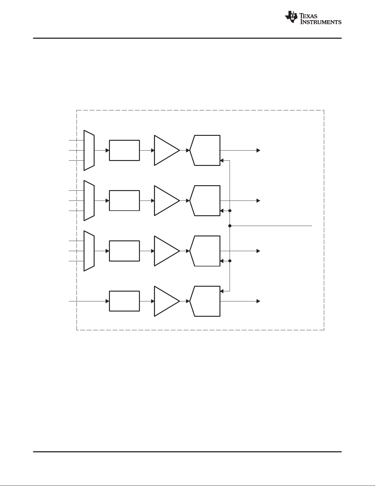
2.1 Analog Processing and A/D Converters
Figure 2-1 shows a functional diagram of the analog processors and ADCs. This block provides the
analog interface to all video inputs. It accepts up to ten inputs and performs source selection, video
clamping, video amplification, A/D conversion, and gain and offset adjustments to center the digitized
video signal.
www.ti.com
Figure 2-1. Analog Processors and A/D Converters
16 Functional Description Copyright © 2005–2010, Texas Instruments Incorporated
Submit Documentation Feedback
Product Folder Link(s): TVP5146M2

TVP5146M2
www.ti.com
2.1.1 Video Input Switch Control
The TVP5146M2 decoder has four analog channels that accept up to ten video inputs. The user can
configure the internal analog video switches via the I2C interface. The ten analog video inputs can be used
for different input configurations, some of which are:
• Up to ten selectable individual composite video inputs, as well as other combinations of YPbPr,
S-Video, and SCART can be supported (see Table 2-12)
The input selection is performed by the input select register at I2C subaddress 00h (see Table 2-12).
2.1.2 Analog Input Clamping
An internal clamping circuit restores the ac-coupled video signal to a fixed dc level. The clamping circuit
provides line-by-line restoration of the video sync level to a fixed dc reference voltage. The selection
between bottom and mid clamp is performed automatically by the TVP5146M2 decoder.
2.1.3 Automatic Gain Control
The TVP5146M2 decoder uses four programmable gain amplifiers (PGAs), one per channel. The PGA
can scale a signal with a voltage-input compliance of 0.5 VPPto 2 VPPto a full-scale 10-bit A/D output
code range. A 4-bit code sets the coarse gain with individual adjustment per channel. Minimum gain
corresponds to a code 0x0 (2-VPP full-scale input, –6-dB gain) while maximum gain corresponds to code
0xF (0.5-VPP full scale, +6-dB gain). The TVP5146M2 decoder also has 12-bit fine gain controls for each
channel and applies them independently to coarse gain controls. For composite video, the input video
signal amplitude can vary significantly from the nominal level of 1 VPP. The TVP5146M2 decoder can
adjust its PGA setting automatically: an AGC can be enabled and can adjust the signal amplitude such
that the maximum range of the ADC is reached without clipping. Some nonstandard video signals contain
peak white levels that saturate the ADC. In these cases, the AGC automatically cuts back gain to avoid
clipping. If the AGC is on, then the TVP5146M2 decoder can read the gain currently being used.
SLES141F–JULY 2005–REVISED NOVEMBER 2010
The TVP5146M2 AGC comprises the front-end AGC before Y/C separation and the back-end AGC after
Y/C separation. The back-end AGC restores the optimum system gain whenever an amplitude reference,
such as the composite peak (which is only relevant before Y/C separation), forces the front-end AGC to
set the gain too low. The front-end and back-end AGC algorithms can use up to four amplitude references:
sync height, color burst amplitude, composite peak, and luma peak.
The specific amplitude references being used by the front-end and back-end AGC algorithms can be
independently controlled using the AGC white peak processing register located at subaddress 74h. The
TVP5146M2 gain increment speed and gain increment delay can be controlled using the AGC increment
speed register located at subaddress 78h and the AGC increment delay register located at subaddress
79h, respectively.
2.1.4 ADCs
All ADCs have a resolution of 11 bits and can operate up to 30 MSPS. All A/D channels receive an
identical clock from the on-chip phase-locked loop (PLL) at a frequency between 24 MHz and 30 MHz. All
ADC reference voltages are generated internally.
2.2 Digital Video Processing
Figure 2-2 is a block diagram of the TVP5146M2 digital video decoder processor. This processor receives
digitized video signals from the ADCs and performs composite processing for CVBS and S-Video inputs,
YCbCr signal enhancements for CVBS and S-Video inputs, and YPbPr/RGB processing for component
video inputs. It also generates horizontal and vertical syncs and other output control signals, such as
genlock for CVBS and S-Video inputs. Additionally, it can provide field identification, horizontal and vertical
lock, vertical blanking, and active video window indication signals. The digital data output can be
Copyright © 2005–2010, Texas Instruments Incorporated Functional Description 17
Submit Documentation Feedback
Product Folder Link(s): TVP5146M2
Copy
Protection
Detector
VBI Data
Processor
Output
Formatter
Composite
Processor
CVBS/Y
C
YCbCr
Y[9:0]
Timing
Processor
AVID
FID
GLCO
XTAL1
XTAL2
RESETB
Component
Processor
CH1 A/D
CH2 A/D
CH3 A/D
Pr/R
Pb/B
Y/G
YCbCr
FSS
HS/CS
VS/VBLK
DATACLK
C[9:0]
CH4 A/D
CVBS/Y/G
Host
Interface
SCL
SDA
Slice VBI Data
2
Decimation
PWDN
2
Decimation
2
Decimation
2
Decimation
TVP5146M2
SLES141F–JULY 2005–REVISED NOVEMBER 2010
programmed to two formats: 20-bit 4:2:2 with external syncs or 10-bit 4:2:2 with embedded/separate
syncs. The circuit detects pseudosync pulses, AGC pulses, and color striping in Macrovision-encoded
copy-protected material. Information present in the VBI interval can be retrieved and either inserted in the
ITU-R BT.656 output as ancillary data or stored in internal FIFO and/or registers for retrieval via the host
port interface.
www.ti.com
Figure 2-2. Digital Video Processing Block Diagram
2.2.1 2x Decimation Filter
All input signals are oversampled by a factor of two (27 MHz). The A/D outputs first pass through
decimation filters that reduce the data rate to 1× the pixel rate. The decimation filter is a half-band filter.
Oversampling and decimation filtering can effectively increase the overall signal-to-noise ratio by 3 dB.
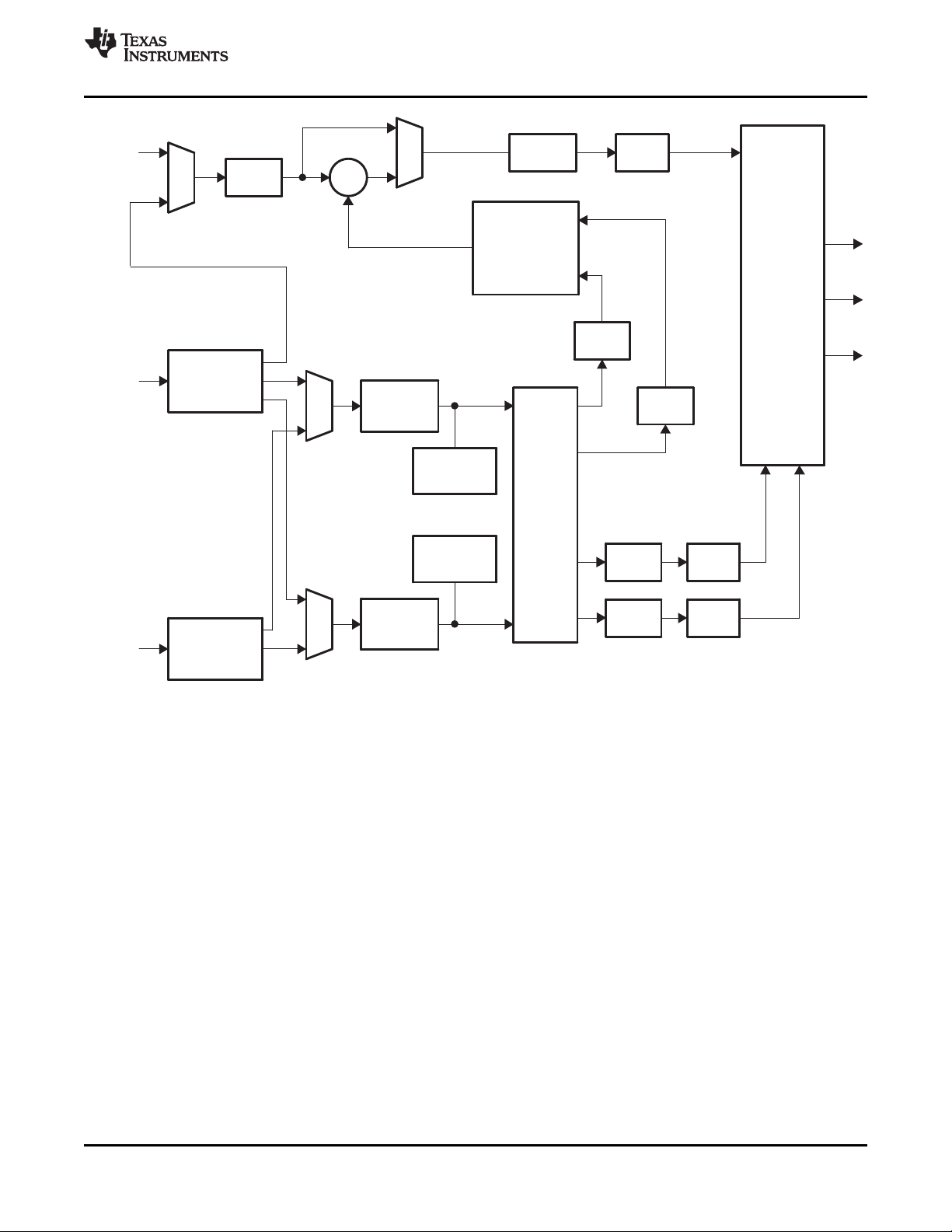
2.2.2 Composite Processor
Figure 2-3 is a block diagram of the TVP5146M2 digital composite video processing circuit. This circuit
receives a digitized composite or S-Video signal from the ADCs and performs Y/C separation (bypassed
for S-Video input), chroma demodulation for PAL/NTSC and SECAM, and YUV signal enhancements.
The 10-bit composite video is multiplied by the subcarrier signals in the quadrature demodulator to
generate color difference signals U and V. The U and V signals are then sent to low-pass filters to achieve
the desired bandwidth. An adaptive 5-line comb filter separates UV from Y based on the unique property
of color phase shifts from line to line. The chroma is remodulated through a quadrature modulator and
subtracted from line-delayed composite video to generate luma. This form of Y/C separation is completely
complementary, thus there is no loss of information. However, in some applications, it is desirable to limit
the U/V bandwidth to avoid crosstalk. In that case, notch filters can be turned on. To accommodate some
viewing preferences, a peaking filter is also available in the luma path. Contrast, brightness, sharpness,
hue, and saturation controls are programmable through the host port.
18 Functional Description Copyright © 2005–2010, Texas Instruments Incorporated
Submit Documentation Feedback
Product Folder Link(s): TVP5146M2
Line
Delay
–
Peaking
NTSC/PAL
Remodulation
NTSC/PAL
Demodulation
Notch
Filter
Color LPF
↓ 2
5-Line
Adaptive
Comb
Filter
Notch
Filter
Notch
Filter
Notch
Filter
Contrast
Brightness
Saturation
Adjust
Cr
Y
Cb
Y
Burst
Accumulator
(U)
U
SECAM
Color
Demodulation
V
Delay
CVBS/Y
SECAM Luma
CVBS
CVBS/C
Color LPF
↓ 2
Burst
Accumulator
(V)
U
V
Delay
Delay
TVP5146M2
www.ti.com
SLES141F–JULY 2005–REVISED NOVEMBER 2010
Figure 2-3. Composite and S-Video Processor
Copyright © 2005–2010, Texas Instruments Incorporated Functional Description 19
Submit Documentation Feedback
Product Folder Link(s): TVP5146M2
f − Frequency − MHz
−70
−60
−50
−40
−30
−20
−10
0
10
0.0 0.5 1.0 1.5 2.0 2.5 3.0 3.5 4.0
ITU-R BT.601 −3 dB
at 1.42 MHz
Amplitude − dB
f − Frequency − MHz
−70
−60
−50
−40
−30
−20
−10
0
10
0.0 0.5 1.0 1.5 2.0 2.5 3.0 3.5 4.0
Amplitude − dB
Filter 3
−3 dB at 554 kHz
Filter 2
−3 dB at 844 kHz
Filter 1
−3 dB
at 1.03 MHz
Filter 0
−3 dB at 1.41 MHz
TVP5146M2
SLES141F–JULY 2005–REVISED NOVEMBER 2010
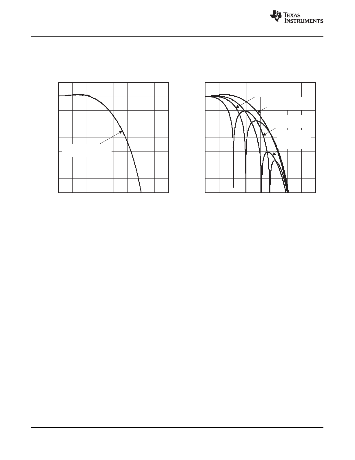
2.2.2.1 Color Low-Pass Filter
High filter bandwidth preserves sharp color transitions and produces crisp color boundaries. However, for
video sources that have asymmetrical U and V side bands, it is desirable to limit the filter bandwidth to
avoid UV crosstalk. The color low-pass filter bandwidth is programmable to enable one of the three notch
filters. Figure 2-4 and Figure 2-5 represent the frequency responses of the wideband color low-pass filters.
www.ti.com
Figure 2-4. Color Low-Pass Filter Frequency Figure 2-5. Color Low-Pass Filter With Filter
Response Characteristics, NTSC/PAL ITU-R BT.601 Sampling
20 Functional Description Copyright © 2005–2010, Texas Instruments Incorporated
Submit Documentation Feedback
Product Folder Link(s): TVP5146M2
f − Frequency − MHz
−40
−35
−30
−25
−20
−15
−10
−5
0
5
10
0 1 2 3 4 5 6 7
No Notch Filter
Notch 3 Filter
Notch 1 Filter
Amplitude − dB
Notch 2 Filter
−40
−35
−30
−25
−20
−15
−10
−5
0
5
10
0 1 2 3 4 5 6 7
f − Frequency − MHz
Amplitude − dB
No Notch Filter
Notch 2 Filter
Notch 1 Filter
Notch 3 Filter
TVP5146M2
www.ti.com
2.2.2.2 Y/C Separation
Y/C separation can be done using adaptive 5-line (5-H delay) comb filters or a chroma trap filter. The
comb filter can be selectively bypassed in the luma or chroma path. If the comb filter is bypassed in the
luma path, chroma trap filters are used which are shown in Figure 2-6 and Figure 2-7. The TI patented
adaptive comb filter algorithm reduces artifacts such as hanging dots at color boundaries. It detects and
properly handles false colors in high frequency luminance images, such as a multiburst pattern or circle
pattern. Adaptive comb filtering is the recommended mode of operation.
SLES141F–JULY 2005–REVISED NOVEMBER 2010
Figure 2-6. Chroma Trap Filter Frequency Response, Figure 2-7. Chroma Trap Filter Frequency Response,
NTSC ITU-R BT.601 Sampling PAL ITU-R BT.601 Sampling
Copyright © 2005–2010, Texas Instruments Incorporated Functional Description 21
Submit Documentation Feedback
Product Folder Link(s): TVP5146M2
Bandpass
Filter
x
Gain
Peaking
Filter
IN
+
OUT
Delay
Peak
Detector
f – Frequency – MHz
−1
0
1
2
3
4
5
6
7
0 1 2 3 4 5 6 7
Gain = 0
Gain = 2
Gain = 1
Gain = 0.5
Peak at
f = 2.64 MHz
Amplitude − dB
TVP5146M2
SLES141F–JULY 2005–REVISED NOVEMBER 2010
2.2.3 Luminance Processing
The digitized composite video signal passes through either a luminance comb filter or a chroma trap filter,
either of which removes chrominance information from the composite signal to generate a luminance
signal. The luminance signal is then fed into the input of a peaking circuit. Figure 2-8 illustrates the basic
functions of the luminance data path. In the case of S-Video, the luminance signal bypasses the comb
filter or chroma trap filter and is fed directly to the circuit. High-frequency components of the luminance
signal are enhanced by a peaking filter (sharpness). Figure 2-9 shows the characteristics of the peaking
filter at four different gain settings that are programmable via the host port.
Figure 2-8. Luminance Edge-Enhancer Peaking Block Diagram
www.ti.com
2.2.4 Color Transient Improvement (CTI)
CTI enhances horizontal color transients by delay modulation for both color difference signals. The
operation must be performed only on YCbCr-formatted data. The color difference signal transition points
are maintained, but the edges are enhanced for signals that have bandwidth-limited color components (for
example, CVBS and S-Video).
22 Functional Description Copyright © 2005–2010, Texas Instruments Incorporated
Figure 2-9. Peaking Filter Response, NTSC/PAL ITU-R BT.601 Sampling
Submit Documentation Feedback
Product Folder Link(s): TVP5146M2
x
Gain
Y
Y
Limit+
Offset
x
Gain
CbCr
CbCr
Limit
TVP5146M2
www.ti.com
2.2.5 Component Video Processor
The component video processing block supports a user-selectable contrast, brightness, and saturation
adjustment in YCbCr output formats. For YCbCr output formats, gain and offset values are applied to the
luma data path to map the pixel values to the correct output range (for 10-bit Y
and to provide a means of adjusting contrast and brightness. For Y, digital contrast (gain) and brightness
(offset) factors can vary from 0 to 255. The contrast control adjusts the amplitude range of the Y output
centered at the midpoint of the output code range. The limit block limits the output to the ITU-R BT.601
range (Y
For CbCr components, a saturation (gain) factor is applied to the CbCr inputs to map them to the CbCr
output code range and provide saturation control. Similarly, the limit block can limit CbCr outputs to a valid
range:
Cb,Cr
to Y
min
= 64 / Cb,Cr
min
) or an extended range, depending on a user setting.
max
Figure 2-10. Y Component Gain, Offset, Limit
= 960
max
SLES141F–JULY 2005–REVISED NOVEMBER 2010
= 64 and Y
min
max
= 940),
Figure 2-11. CbCr Component Gain, Offset, Limit
2.2.6 Color Space Conversion
The formulas for RGB to YCbCr conversion are given as:
Y = 0.299 × R + 0.587 × G + 0.114 × B
Cb = –0.172 × R – 0.339 × G + 0.511 × B + 512
Cr = 0.511 × R – 0.428 × G – 0.083 × B + 512
2.3 Clock Circuits
An internal line-locked PLL generates the system and pixel clocks. A 14.31818-MHz clock is required to
drive the PLL. This can be input to the TVP5146M2 decoder at the 1.8-V level on terminal 74 (XTAL1), or
a crystal of 14.31818-MHz fundamental resonant frequency can be connected across terminals 74 and 75
(XTAL2). If a parallel resonant circuit is used as shown in Figure 2-12, then the external capacitors must
have the following relationship:
CL1= CL2= 2CL− C
Where,
C
is the terminal capacitance with respect to ground
STRAY
CLis the crystal load capacitance specified by the crystal manufacturer
Figure 2-12 shows the reference clock configurations. The TVP5146M2 decoder generates the DATACLK
signal used for clocking data.
STRAY
(1)
Copyright © 2005–2010, Texas Instruments Incorporated Functional Description 23
Submit Documentation Feedback
Product Folder Link(s): TVP5146M2
TVP5146M2
74
XTAL1
14.31818-MHz
Crystal
75
XTAL2
TVP5146M2
74
XTAL1
75
XTAL2
C
L1
C
L2
14.31818-MHz
1.8-V Clock
NC
R
RTC
45 CLK18 CLK
L
S
B
0
3 CLK128 CLK
23-Bit Fsc PLL Increment
Start
Bit
1 CLK
RS
Invalid
Sample
Valid
Sample
M
S
B
22
Reserved
TVP5146M2
SLES141F–JULY 2005–REVISED NOVEMBER 2010
Figure 2-12. Reference Clock Configurations
2.4 Real-Time Control (RTC)
Although the TVP5146M2 decoder is a line-locked system, the color-burst information is used to
determine accurately the color subcarrier frequency and phase. This ensures proper operation with
nonstandard video signals that do not follow exactly the required frequency multiple between color
subcarrier frequency and video line frequency. The frequency control word of the internal color subcarrier
PLL and the subcarrier reset bit are transmitted via terminal 37 (GLCO) for optional use in an end system
(for example, by a video encoder). The frequency control word is a 23-bit binary number. The
instantaneous frequency of the color subcarrier can be calculated from the following equation:
F
= (F
PLL
Where,
F
F
F
Figure 2-13 shows the detailed timing diagram.
/ 223) × F
ctrl
is the frequency of the subcarrier PLL
PLL
is the 23-bit PLL frequency control word
ctrl
is two times the pixel frequency
sclk
sclk
www.ti.com
(2)
24 Functional Description Copyright © 2005–2010, Texas Instruments Incorporated
NOTE: RTC reset bit (R) is active-low, Sequence bit (S) PAL: 1 = (R-Y) line normal, 0 = (R-Y) line inverted, NTSC: 1 = no
change
Figure 2-13. RTC Timing
Submit Documentation Feedback
Product Folder Link(s): TVP5146M2
TVP5146M2
www.ti.com
2.5 Output Formatter
The output formatter sets how the data is formatted for output on the TVP5146M2 output buses. Table 2-1
shows the available output modes.
TERMINAL NAME TERMINAL NUMBER 10-Bit 4:2:2 YCbCr 20-Bit 4:2:2 YCbCr
Y_9 43 Cb9, Y9, Cr9 Y9
Y_8 44 Cb8, Y8, Cr8 Y8
Y_7 45 Cb7, Y7, Cr7 Y7
Y_6 46 Cb6, Y6, Cr6 Y6
Y_5 47 Cb5, Y5, Cr5 Y5
Y_4 50 Cb4, Y4, Cr4 Y4
Y_3 51 Cb3, Y3, Cr3 Y3
Y_2 52 Cb2, Y2, Cr2 Y2
Y_1 53 Cb1, Y1, Cr1 Y1
Y_0 54 Cb0, Y0, Cr0 Y0
C_9 57 Cb9, Cr9
C_8 58 Cb8, Cr8
C_7 59 Cb7, Cr7
C_6 60 Cb6, Cr6
C_5 63 Cb5, Cr5
C_4 64 Cb4, Cr4
C_3 65 Cb3, Cr3
C_2 66 Cb2, Cr2
C_1 69 Cb1, Cr1
C_0 70 Cb0, Cr0
SLES141F–JULY 2005–REVISED NOVEMBER 2010
Table 2-1. Output Format
Table 2-2. Summary of Line Frequencies, Data Rates, and Pixel/Line Counts
STANDARDS FREQUENCY LINE RATE
601 Sampling
NTSC-J, M 858 720 525 13.5 3.579545 15.73426
NTSC-4.43 858 720 525 13.5 4.43361875 15.73426
PAL-M 858 720 525 13.5 3.57561149 15.73426
PAL-60 858 720 525 13.5 4.43361875 15.73426
PAL-B, D, G, H, I 864 720 625 13.5 4.43361875 15.625
PAL-N 864 720 625 13.5 4.43361875 15.625
PAL-Nc 864 720 625 13.5 3.58205625 15.625
SECAM 864 720 625 13.5 15.625
Copyright © 2005–2010, Texas Instruments Incorporated Functional Description 25
PIXELS PER ACTIVE PIXELS LINES PER SUBCARRIER
LINE PER LINE FRAME FREQUENCY
Submit Documentation Feedback
Product Folder Link(s): TVP5146M2
PIXEL HORIZONTAL
(MHz) (kHz)
COLOR
(MHz)
Dr = 4.406250
Db = 4.250000

TVP5146M2
SLES141F–JULY 2005–REVISED NOVEMBER 2010
2.5.1 Fast Switches for SCART
The TVP5146M2 decoder supports the SCART interface used in European audio/video end equipment to
carry composite video, S-Video, and RGB video on the same cable. If composite video and RGB video are
present simultaneously on the video terminals assigned to a SCART interface, the TVP5146M2 decoder
assumes they are pixel synchronous to each other. The timing for both composite video and RGB video is
obtained from the composite source, and its derived clock is used to sample RGB video as well. The
fast-switch input terminal allows switching between these two input video sources on a pixel-by-pixel
basis. The fast switch is a hard switch; there is no alpha blending between both sources.
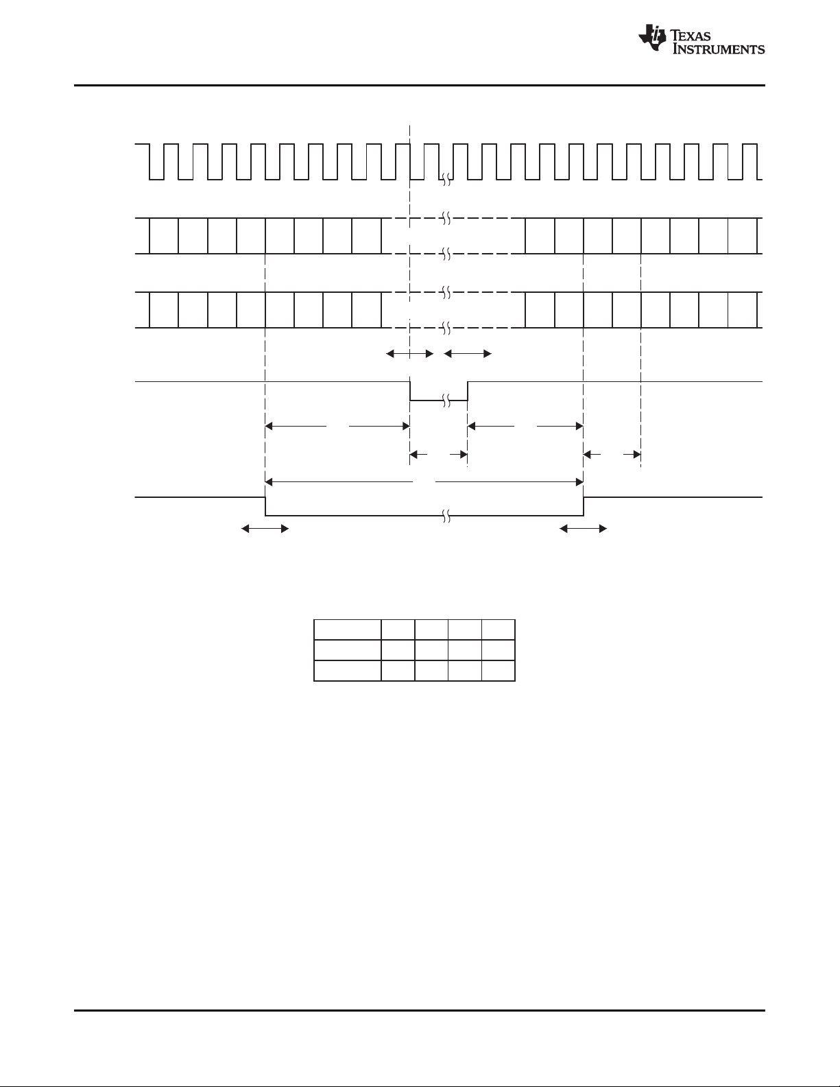
2.5.2 Separate Syncs
VS, HS, and VBLK are independently software programmable to a 1× pixel count. This allows any
possible alignment to the internal pixel count and line count. The default settings for 525-line and 625-line
video outputs are given in Figure 2-14 and Figure 2-15. FID changes at the same transient time when the
trailing edge of vertical sync occurs. The polarity of FID is programmable by an I2C interface.
www.ti.com
26 Functional Description Copyright © 2005–2010, Texas Instruments Incorporated
Submit Documentation Feedback
Product Folder Link(s): TVP5146M2
First Field V ideo
525
VS
VBLK
FID
1 2 3 4 5 6 7 8 9 10 11 21 22
525 Line
HS
VS Start VS Stop
CS
VBLK Start VBLK Stop
Second Field V ideo
262
VS
VBLK
FID
263 264 265 266 267 268 269 270 271 272 273 284 285
HS
VS Start VS Stop
CS
VBLK Start VBLK Stop
TVP5146M2
www.ti.com
SLES141F–JULY 2005–REVISED NOVEMBER 2010
NOTE: Line numbering conforms to ITU-R BT.470.
Figure 2-14. Vertical Synchronization Signals for 525-Line System
Copyright © 2005–2010, Texas Instruments Incorporated Functional Description 27
Submit Documentation Feedback
Product Folder Link(s): TVP5146M2
First Field V ideo
VS
VBLK
FID
625 Line
HS
VS Start VS Stop
CS
VBLK Start VBLK Stop
Second Field V ideo
310
VS
VBLK
FID
311 312 313 314 315 316 317 318 319 320 321 336 337
HS
VS Start VS Stop
CS
VBLK Start VBLK Stop
622 623 624 625 1 2 3 4 5 6 7 23 24 258
338
TVP5146M2
SLES141F–JULY 2005–REVISED NOVEMBER 2010
www.ti.com
NOTE: Line numbering conforms to ITU-R BT.470.
Figure 2-15. Vertical Synchronization Signals for 625-Line System
28 Functional Description Copyright © 2005–2010, Texas Instruments Incorporated
Submit Documentation Feedback
Product Folder Link(s): TVP5146M2
NTSC 601 106
PAL 601 112
128
1284248
276
288
Y[9:0]
DATACLK = 2 Pixel Clock
Mode A B C D
Cb
DATACLK
EAV
1
Y Cr Y
EAV
2
EAV3EAV
4
SAV1SAV2SAV3SAV
4
Cb0 Y0 Cr0 Y1
0
HS Start
Horizontal Blanking
HS
HS Stop
A C
B
AVID
D
AVID Stop AVID Start
TVP5146M2
www.ti.com
SLES141F–JULY 2005–REVISED NOVEMBER 2010
NOTE: ITU-R BT.656 10-bit 4:2:2 timing with 2× pixel clock reference
Figure 2-16. Horizontal Synchronization Signals for 10-Bit 4:2:2 Mode
Copyright © 2005–2010, Texas Instruments Incorporated Functional Description 29
Submit Documentation Feedback
Product Folder Link(s): TVP5146M2
22
53 64 19
56
CbCr[9:0]
NTSC 601
PAL 601
DATACLK = 1 Pixel Clock
64
Mode A B C
136
142
D
Cb
DATACLK
Cr Cb Cr Cb0 Cr0 Cb1 Cr1
0
HS Start
Horizontal Blanking
HS
HS Stop
A C
B
AVID
D
NOTE: AVID rising edge occurs 2 clock cycles early.
Y[9:0]
Y Y Y Y Y0 Y1 Y2 Y3Horizontal Blanking
2
AVID Stop AVID Start
TVP5146M2
SLES141F–JULY 2005–REVISED NOVEMBER 2010
www.ti.com
NOTE: 20-bit 4:2:2 timing with 1× pixel clock reference
Figure 2-17. Horizontal Synchronization Signals for 20-Bit 4:2:2 Mode
30 Functional Description Copyright © 2005–2010, Texas Instruments Incorporated
Submit Documentation Feedback
Product Folder Link(s): TVP5146M2

NTSC 601 64
PAL 601
10-Bit (PCLK = 2 Pixel Clock)
64
Mode
B/2
First Field B/2
858
864
H/2
32
20-Bit (PCLK = 1 Pixel Clock)
32
B/2
429
432
H/2
HS
VS
Second Field
HS
VS
B/2
H/2 + B/2 H/2 + B/2
TVP5146M2
www.ti.com
SLES141F–JULY 2005–REVISED NOVEMBER 2010
Figure 2-18. VSYNC Position With Respect to HSYNC
2.5.3 Embedded Syncs
Standards with embedded syncs insert the SAV and EAV codes into the data stream on the rising and
falling edges of AVID. These codes contain the V and F bits, which also define vertical timing. Table 2-3
gives the format of the SAV and EAV codes.
H equals 1 always indicates EAV. H equals 0 always indicates SAV. The alignment of V and F to the line
and field counter varies depending on the standard.
The P bits are protection bits:
Preamble 1 1 1 1 1 1 1 1 1 1
Preamble 0 0 0 0 0 0 0 0 0 0
Preamble 0 0 0 0 0 0 0 0 0 0
Status word 1 F V H P3 P2 P1 P0 0 0
P3 = V xor H; P2 = F xor H; P1 = F xor V; P0 = F xor V xor H
D9 (MSB) D8 D7 D6 D5 D4 D3 D2 D1 D0
Table 2-3. EAV and SAV Sequence
Copyright © 2005–2010, Texas Instruments Incorporated Functional Description 31
Submit Documentation Feedback
Product Folder Link(s): TVP5146M2

TVP5146M2
SLES141F–JULY 2005–REVISED NOVEMBER 2010
2.6 I2C Host Interface
Communication with the TVP5146M2 decoder is via an I2C host interface. The I2C standard consists of
two signals, the serial input/output data (SDA) line and the serial input clock line (SCL), which carry
information between the devices connected to the bus. A third signal (I2CA) is used for slave address
selection. Although an I2C system can be multimastered, the TVP5146M2 decoder functions as a slave
device only.
Because SDA and SCL are kept open drain at a logic-high output level or when the bus is not driven, the
user must connect SDA and SCL to a positive supply voltage via a pullup resistor on the board. The slave
addresses select signal, terminal 37 (I2CA), enables the use of two TVP5146M2 devices tied to the same
I2C bus, because it controls the least-significant bit of the I2C device address.
Table 2-4. I2C Host Interface Terminal Description
SIGNAL TYPE DESCRIPTION
I2CA I Slave address selection
SCL I/O Input/output clock line
SDA I/O Input/output data line
2.6.1 Reset and I2C Bus Address Selection
The TVP5146M2 decoder can respond to two possible chip addresses. The address selection is made at
reset by an externally supplied level on the I2CA terminal. The TVP5146M2 decoder samples the level of
terminal 37 at power up or at the trailing edge of RESETB and configures the I2C bus address bit A0.
www.ti.com
Table 2-5. I2C Address Selection
A6 A5 A4 A3 A2 A1 A0 (I2CA) R/W HEX
1 0 1 1 1 0 0 (default) 1/0 B9/B8
1 0 1 1 1 0 1
(1) If terminal 37 is strapped to DVDD via a 2.2-kΩ resistor, I2C device address A0 is set to 1.
(1)
1/0 BB/BA
2.6.2 I2C Operation
Data transfers occur using the following illustrated formats.
S 10111000 ACK Subaddress ACK Send Data ACK P
Read from I2C control registers
S 10111000 ACK Subaddress ACK S 10111001 ACK Receive Data NAK P
S = I2C bus start condition
P = I2C bus stop condition
ACK = Acknowledge generated by the slave
NAK = Acknowledge generated by the master, for multiple-byte read master with ACK each
byte except last byte
Subaddress = Subaddress byte
Data = Data byte. If more than one byte of data is transmitted (read and write), the
subaddress pointer is automatically incremented.
I2C bus address = Example shown that I2CA is in default mode [write (B8h), read (B9h)]
32 Functional Description Copyright © 2005–2010, Texas Instruments Incorporated
Submit Documentation Feedback
Product Folder Link(s): TVP5146M2

Single Byte
B8S ACK E8 ACK VA0 ACK VA1 ACK VA2 ACK P
VBUS Write
B8S ACK E0 ACK Send Data ACK P
Multiple Bytes
B8
S ACK E8 ACK VA0 ACK VA1 ACK VA2 ACK P
B8S ACK E1 ACK Send Data ACK ACK PSend Data• ••
Single Byte
B8
S ACK E8 ACK VA0 ACK VA1 ACK VA2 ACK P
VBUS Read
B8S ACK E0 ACK ACK
Multiple Bytes
B8
S ACK E8 ACK VA0 ACK VA1 ACK VA2 ACK P
B8S ACK E1 ACK ACK NAK PRead Data•••
Read Data NAK PS B9
S B9 ACK Read Data
HOST
Processor
I2C
VBUS
Data
I2C Registers
00h
E0h
E1h
VBUS
Address
E8h
EAh
FFh
VBUS[23:0]
Line Mode
VBUS Registers
00 0000h
FIFO
VPS/Gemstar
VITC
WSS/CGMS
CC
80 051Ch
80 0520h
80 052Ch
80 0600h
80 0700h
90 1904h
FF FFFFh
NOTE: Examples use default I2C address.
ACK = Acknowledge generated by the slave
NAK = No Acknowledge generated by the master
TVP5146M2
www.ti.com
2.6.3 VBUS Access
The TVP5146M2 decoder has additional internal registers accessible through an indirect access to an
internal 24-bit address wide VBUS. Figure 2-19 shows the VBUS register access.
SLES141F–JULY 2005–REVISED NOVEMBER 2010
Copyright © 2005–2010, Texas Instruments Incorporated Functional Description 33
Figure 2-19. VBUS Access
Submit Documentation Feedback
Product Folder Link(s): TVP5146M2

TVP5146M2
SLES141F–JULY 2005–REVISED NOVEMBER 2010
2.6.4 I2C Timing Requirements
The TVP5146M2 decoder requires delays in the I2C accesses to accommodate the internal processor
timing. In accordance with I2C specifications, the TVP5146M2 decoder holds the I2C clock line (SCL) low
to indicate the wait period to the I2C master. If the I2C master is not designed to check for the I2C clock
line held-low condition, then the maximum delays must always be inserted where required. These delays
are of variable length; maximum delays are indicated in the following diagram:
Normal register
S 10111000 ACK Subaddress ACK Send Data ACK ...Wait 64 µs... P
2.7 VBI Data Processor
The TVP5146M2 VDP slices various data services such as teletext (WST, NABTS), closed caption (CC),
wide screen signaling (WSS), program delivery control (PDC), vertical interval time code (VITC), video
program system (VPS), copy generation management system (CGMS) data, and electronic program guide
(EPG or Gemstar) 1x/2x. Table 2-6 shows the supported VBI system.
These services are acquired by programming the VDP to enable the reception of one or more VBI data
standard(s) in the VBI. The VDP can be programmed on a line-per-line basis to enable simultaneous
reception of different VBI formats, one per line. The results are stored in a FIFO and/or registers. Because
of its high data bandwidth, the teletext results are stored in FIFO only. The TVP5146M2 decoder provides
fully decoded V-Chip data to the dedicated registers at subaddresses 800540h to 800543h (see
Table 2-115 through Table 2-118).
www.ti.com
Table 2-6. Supported VBI System
VBI SYSTEM STANDARD LINE NUMBER NUMBER OF BYTES
Teletext WST A SECAM 6-23 (Fields 1 and 2) 38
Teletext WST B PAL 6-22 (Fields 1 and 2) 43
Teletext NABTS C NTSC 10-21 (Fields 1 and 2) 34
Teletext NABTS D NTSC-J 10-21 (Fields 1 and 2) 35
Closed Caption PAL 22 (Fields 1 and 2) 2
Closed Caption NTSC 21 (Fields 1 and 2) 2
WSS-CGMS PAL 23 (Fields 1 and 2) 14 bits
WSS-CGMS NTSC 20 (Fields 1 and 2) 20 bits
VITC PAL 6-22 9
VITC NTSC 10-20 9
VPS (PDC) PAL 16 13
V-Chip (decoded) NTSC 21 (Field 2) 2
Gemstar 1x NTSC 2
Gemstar 2x NTSC 5 with frame byte
User Any Programmable Programmable
34 Functional Description Copyright © 2005–2010, Texas Instruments Incorporated
Submit Documentation Feedback
Product Folder Link(s): TVP5146M2

TVP5146M2
www.ti.com
SLES141F–JULY 2005–REVISED NOVEMBER 2010
2.7.1 VBI FIFO and Ancillary Data in Video Stream
Sliced VBI data can be output as ancillary data in the video stream in ITU-R BT.656 mode. VBI data is
output on the Y_[9:2] terminals during the horizontal blanking period. Table 2-7 shows the header format
and sequence of the ancillary data inserted into the video stream. This format is also used to store any
VBI data into the FIFO. The size of the FIFO is 512 bytes. Therefore, the FIFO can store up to 11 lines of
teletext data with the NTSC NABTS standard.
Table 2-7. Ancillary Data Format and Sequence
BYTE NO. D6 D5 D4 D3 D2 D1 DESCRIPTION
0 0 0 0 0 0 0 0 0
1 1 1 1 1 1 1 1 1 Ancillary data preamble
2 1 1 1 1 1 1 1 1
3 NEP EP 0 1 0 DID2 DID1 DID0 Data ID (DID)
4 NEP EP F5 F4 F3 F2 F1 F0 Secondary data ID (SDID)
5 NEP EP N5 N4 N3 N2 N1 N0 Number of 32 bit data (NN)
6 Video line # [7:0] Internal data ID0 (IDID0)
7 0 0 0 Data error Match #1 Match #2 Video line # [9:8] Internal data ID1 (IDID1)
8 1. Data Data byte 1st word
9 2. Data Data byte
10 3. Data Data byte
11 4. Data Data byte
⋮ ⋮ ⋮
4N+7 0 0 0 0 0 0 0 0 Fill byte
D7 D0
(MSB) (LSB)
m. Data Data byte Nth word
CS[7:0] Check sum
EP: Even parity for D0-D5
NEP: Negated even parity
DID: 91h: Sliced data of VBI lines of first field
53h: Sliced data of line 24 to end of first field
55h: Sliced data of VBI lines of second field
97h: Sliced data of line 24 to end of second field
SDID: This field holds the data format taken from the line mode register bits [2:0] of the corresponding line.
NN: Number of Dwords beginning with byte 8 through 4N+7. This value is the number of Dwords where each Dword is 4 bytes.
IDID0: Transaction video line number [7:0]
IDID1: Bit 0/1 = Transaction video line number [9:8]
Bit 2 = Match 2 flag
Bit 3 = Match 1 flag
Bit 4 = 1 if an error was detected in the EDC block.0 if no error was detected.
CS: Sum of D0-D7 of DID through last data byte
Fill byte: Fill bytes make a multiple of four bytes from byte 0 to last fill byte. For teletext modes, byte 8 is the sync pattern byte. Byte 9 is
the first data byte.
Copyright © 2005–2010, Texas Instruments Incorporated Functional Description 35
Submit Documentation Feedback
Product Folder Link(s): TVP5146M2

TVP5146M2
SLES141F–JULY 2005–REVISED NOVEMBER 2010
2.7.2 VBI Raw Data Output
The TVP5146M2 decoder can output raw A/D video data at twice the sampling rate for external VBI
slicing. This is transmitted as an ancillary data block, although somewhat differently from the way the
sliced VBI data is transmitted in the FIFO format as described in Section 2.7.1. The samples are
transmitted during the active portion of the line. VBI raw data uses ITU-R BT.656 format having only luma
data. The chroma samples are replaced by luma samples. The TVP5146M2 decoder inserts a four-byte
preamble 000h 3FFh 3FFh 180h before data start. There are no checksum bytes and fill bytes in this
mode.
Table 2-8. VBI Raw Data Output Format
BYTE D9 D0
NO. (MSB) (LSB)
0 0 0 0 0 0 0 0 0 0 0
1 1 1 1 1 1 1 1 1 1 1
2 1 1 1 1 1 1 1 1 1 1
3 0 1 1 0 0 0 0 0 0 0
4 1. Data
5 2. Data
⋮ ⋮
n-1 n-5. Data
n n-4. Data
D8 D7 D6 D5 D4 D3 D2 D1 DESCRIPTION
www.ti.com
VBI raw data preamble
2× pixel rate luma data
(i.e., NTSC 601: n = 1707)
2.8 Reset and Initialization
Reset is initiated at power up or any time terminal 34 (RESETB) is brought low. Table 2-9 describes the
status of the TVP5146M2 terminals during and immediately after reset.
Table 2-9. Reset Sequence
SIGNAL NAME DURING RESET RESET COMPLETED
Y_[9:0], C_[9:0]/GPIO Input High impedance
RESETB, PWDN, SDA, SCL, FSS/GPIO, AVID/GPIO, GLCO/I2CA,
HS/CS/GPIO, VS/VBLK/GPIO, FID
INTREQ Input Output
DATACLK Output High impedance
Input Input
36 Functional Description Copyright © 2005–2010, Texas Instruments Incorporated
Submit Documentation Feedback
Product Folder Link(s): TVP5146M2

3 ms (min)
RESETB
(Terminal 34)
1 ms (min)
Invalid I2C Cycle Valid
Normal Operation
100 s
SDA
(Terminal 29)
Power (1.8 V)
Power (3.3 V)
Reset
NOTE: All times shown are minimum values. Maximum time between 1.8 V and 3.3 V should be no longer than 1 second.
TVP5146M2
www.ti.com
TI recommends the following power-up sequence.
The following register writes must be made before normal operation of the device.
Figure 2-20. Reset Timing
STEP
1 0x03 0x01
2 0x03 0x00
I2C I2C
SUBADDRESS DATA
SLES141F–JULY 2005–REVISED NOVEMBER 2010
When using the TVP5146M2I over the industrial (−40°C to 85°C) temperature range, the following register
writes are required following device power up and RESETB to write 0x14 to VBUS register 0xA00014.
This setup is optional when using the TVP5146M2 over the commercial (0°C to 70°C) temperature range.
2.9 Adjusting External Syncs
The proper sequence to program the following external syncs is:
• To set NTSC, PAL-M, NTSC 443, PAL60 (525-line modes):
– Set the video standard to NTSC (register 02h).
– Set HSYNC, VSYNC, VBLK, and AVID external syncs (registers 16h through 24h).
• To set PAL, PAL-N, SECAM (625-line modes):
– Set the video standard to PAL (register 02h).
– Set HSYNC, VSYNC, VBLK, and AVID external syncs (registers 16h through 24h).
• For autoswitch, set the video standard to autoswitch (register 02h).
STEP
1 0xE8 0x14
2 0xE9 0x00
3 0xEA 0xA0
4 0xE0 0x14
I2C I2C
SUBADDRESS DATA
Copyright © 2005–2010, Texas Instruments Incorporated Functional Description 37
Submit Documentation Feedback
Product Folder Link(s): TVP5146M2

TVP5146M2
SLES141F–JULY 2005–REVISED NOVEMBER 2010
www.ti.com
2.10 Internal Control Registers
The TVP5146M2 decoder is initialized and controlled by a set of internal registers that define the operating
parameters of the entire device. Communication between the external controller and the TVP5146M2 is
through a standard I2C host port interface, as previously described. Table 2-10 shows the summary of
these registers. Detailed programming information for each register is described in the following sections.
Additional registers are accessible through an indirect procedure involving access to an internal 24-bit
address wide VBUS. Table 2-11 shows the summary of the VBUS registers.
NOTE
Do not write to reserved registers. Reserved bits in any defined register must be written with
zeros, unless otherwise noted.
Table 2-10. I2C Register Summary
REGISTER NAME DEFAULT R/W
Input select 00h 00h R/W
AFE gain control 01h 0Fh R/W
Video standard 02h 00h R/W
Operation mode 03h 00h R/W
Autoswitch mask 04h 23h R/W
Color killer 05h 10h R/W
Luminance processing control 1 06h 00h R/W
Luminance processing control 2 07h 00h R/W
Luminance processing control 3 08h 02h R/W
Luminance brightness 09h 80h R/W
Luminance contrast 0Ah 80h R/W
Chrominance saturation 0Bh 80h R/W
Chroma hue 0Ch 00h R/W
Chrominance processing control 1 0Dh 00h R/W
Chrominance processing control 2 0Eh 0Eh R/W
Reserved 0Fh
Component Pr saturation 10h 80h R/W
Component Y contrast 11h 80h R/W
Component Pb saturation 12h 80h R/W
Reserved 13h
Component Y brightness 14h 80h R/W
Reserved 15h
AVID start pixel 16h-17h 055h R/W
AVID stop pixel 18h-19h 325h R/W
HSYNC start pixel 1Ah-1Bh 000h R/W
HSYNC stop pixel 1Ch-1Dh 040h R/W
VSYNC start line 1Eh-1Fh 004h R/W
VSYNC stop line 20h-21h 007h R/W
VBLK start line 22h-23h 001h R/W
VBLK stop line 24h-25h 015h R/W
Embedded Sync Offset Control 1 26h 00h R/W
Embedded Sync Offset Control 2 27h 00h R/W
(1)
I2C
SUBADDRESS
(1) R = Read only, W = Write only, R/W = Read and write
Reserved register addresses must not be written to.
38 Functional Description Copyright © 2005–2010, Texas Instruments Incorporated
Submit Documentation Feedback
Product Folder Link(s): TVP5146M2

TVP5146M2
www.ti.com
SLES141F–JULY 2005–REVISED NOVEMBER 2010
Table 2-10. I2C Register Summary (continued)
REGISTER NAME DEFAULT R/W
Fast-switch control 28h CCh R/W
Reserved 29h
Fast-switch SCART delay 2Ah 00h R/W
Reserved 2Bh
SCART delay 2Ch 00h R/W
CTI delay 2Dh 00h R/W
CTI control 2Eh 00h R/W
Brightness and Contrast Range Extender 2Fh 00h R/W
Reserved 30h-31h
Sync control 32h 00h R/W
Output formatter 1 33h 40h R/W
Output formatter 2 34h 00h R/W
Output formatter 3 35h FFh R/W
Output formatter 4 36h FFh R/W
Output formatter 5 37h FFh R/W
Output formatter 6 38h FFh R/W
Clear lost lock detect 39h 00h R/W
Status 1 3Ah R
Status 2 3Bh R
AGC gain status 3Ch-3Dh R
Reserved 3Eh
Video standard status 3Fh R
GPIO input 1 40h R
GPIO input 2 41h R
Reserved 42h-45h R
AFE coarse gain for CH1 46h 20h R/W
AFE coarse gain for CH2 47h 20h R/W
AFE coarse gain for CH3 48h 20h R/W
AFE coarse gain for CH4 49h 20h R/W
AFE fine gain for Pb_B 4Ah-4Bh 900h R/W
AFE fine gain for Y_G_Chroma 4Ch-4Dh 900h R/W
AFE fine gain for Pr_R 4Eh-4Fh 900h R/W
AFE fine gain for CVBS_Luma 50h-51h 900h R/W
Reserved 52h-68h
F-bit and V-bit control 1 69h 00h R/W
Reserved 6Ah-6Bh
Back-end AGC Control 6Ch 08h R/W
Reserved 6Dh-6Eh
AGC decrement speed control 6Fh 04h R/W
ROM version 70h R
Reserved 71h-73h
AGC white peak processing 74h 00h R/W
F-bit and V-bit control 2 75h 16h R/W
VCR trick mode control 76h 8Ah R/W
Horizontal shake increment 77h 64h R/W
AGC increment speed 78h 05h R/W
AGC increment delay 79h 1Eh R/W
I2C
SUBADDRESS
Copyright © 2005–2010, Texas Instruments Incorporated Functional Description 39
Submit Documentation Feedback
Product Folder Link(s): TVP5146M2

TVP5146M2
SLES141F–JULY 2005–REVISED NOVEMBER 2010
www.ti.com
Table 2-10. I2C Register Summary (continued)
REGISTER NAME DEFAULT R/W
Reserved 7Ah-7Fh
Chip ID MSB 80h R
Chip ID LSB 81h R
Reserved 82h
CPLL speed control 83h 09h R/W
Reserved 84h-96h
Status request 97h 00h R/W
Reserved 98h-99h
Vertical line count 9Ah-9Bh R
Reserved 9Ch-9Dh
AGC decrement delay 9Eh 00h R/W
Reserved 9Fh-B0h
VDP TTX filter 1 mask 1 B1h 00h R/W
VDP TTX filter 1 mask 2 B2h 00h R/W
VDP TTX filter 1 mask 3 B3h 00h R/W
VDP TTX filter 1 mask 4 B4h 00h R/W
VDP TTX filter 1 mask 5 B5h 00h R/W
VDP TTX filter 2 mask 1 B6h 00h R/W
VDP TTX filter 2 mask 2 B7h 00h R/W
VDP TTX filter 2 mask 3 B8h 00h R/W
VDP TTX filter 2 mask 4 B9h 00h R/W
VDP TTX filter 2 mask 5 BAh 00h R/W
VDP TTX filter control BBh 00h R/W
VDP FIFO word count BCh R
VDP FIFO interrupt threshold BDh 80h R/W
Reserved BEh
VDP FIFO reset BFh 00h R/W
VDP FIFO output control C0h 00h R/W
VDP line number interrupt C1h 00h R/W
VDP pixel alignment C2h-C3h 01Eh R/W
Reserved C4h-D5h
VDP line start D6h 06h R/W
VDP line stop D7h 1Bh R/W
VDP global line mode D8h FFh R/W
VDP full field enable D9h 00h R/W
VDP full field mode DAh FFh R/W
Reserved DBh-DFh
VBUS data access with no VBUS address increment E0h 00h R/W
VBUS data access with VBUS address increment E1h 00h R/W
FIFO read data E2h R
Reserved E3h-E7h
VBUS address access E8h-EAh 00 0000h R/W
Reserved EBh-EFh
Interrupt raw status 0 F0h
Interrupt raw status 1 F1h
Interrupt status 0 F2h R/W
Interrupt status 1 F3h R/W
I2C
SUBADDRESS
40 Functional Description Copyright © 2005–2010, Texas Instruments Incorporated
Submit Documentation Feedback
Product Folder Link(s): TVP5146M2
TVP5146M2
www.ti.com
SLES141F–JULY 2005–REVISED NOVEMBER 2010
Table 2-10. I2C Register Summary (continued)
REGISTER NAME DEFAULT R/W
Interrupt mask 0 F4h 00h R/W
Interrupt mask 1 F5h 00h R/W
Interrupt clear 0 F6h 00h R/W
Interrupt clear 1 F7h 00h R/W
Reserved F8h-FFh
Table 2-11. VBUS Register Summary
REGISTER NAME I2C SUBADDRESS DEFAULT R/W
Reserved 00 0000h-80 051Bh
VDP closed caption data 80 051Ch-80 051Fh R
VDP WSS/CGMS data 80 0520h-80 0526h R
Reserved 80 0527h-80 052Bh
VDP VITC data 80 052Ch-80 0534h R
Reserved 80 0535h-80 053Fh
VDP V-Chip data 80 0540h-80 0543h R
Reserved 80 0544h-80 05FFh
VDP general line mode and line address 80 0600h-80 0611h 00h, FFh R/W
Reserved 80 0612h-80 06FFh
VDP VPS/Gemstar data 80 070Dh-B0 005Fh R
Interrupt configuration B0 0060h 00h R/W
Reserved B0 0061h-FF FFFFh
(1) Writing any value to a reserved register may cause erroneous operation of the TVP5146M2 decoder. It is recommended not to access
any data to/from reserved registers.
I2C
SUBADDRESS
(1)
Copyright © 2005–2010, Texas Instruments Incorporated Functional Description 41
Submit Documentation Feedback
Product Folder Link(s): TVP5146M2

TVP5146M2
SLES141F–JULY 2005–REVISED NOVEMBER 2010
www.ti.com
2.11 Register Definitions
Table 2-12. Input Select Register
Subaddress 00h
Default 00h
7 6 5 4 3 2 1 0
Input select [7:0]
Ten input terminals can be configured to support composite, S-Video, and component YPbPr or SCART as listed in Table 2-13. Users must
follow this table properly for S-Video and component applications because only the terminal configurations listed in Table 2-13 are
supported.
Table 2-13. Analog Channel and Video Mode Selection
MODE INPUT(S) SELECTED
VI_1_A (default) 0 0 0 0 0 0 0 0 0
VI_1_B 0 0 0 0 0 0 0 1 1
VI_1_C 0 0 0 0 0 0 1 0 2
VI_2_A 0 0 0 0 0 1 0 0 4
CVBS
S-Video
RGB VI_1_B(B), VI_2_B(G), VI_3_B(R) 1 0 0 0 0 1 0 1 85
YPbPr VI_1_B(Pb), VI_2_B(Y), VI_3_B(Pr) 1 0 0 1 0 1 0 1 95
SCART
VI_2_B 0 0 0 0 0 1 0 1 5
VI_2_C 0 0 0 0 0 1 1 0 6
VI_3_A 0 0 0 0 1 0 0 0 8
VI_3_B 0 0 0 0 1 0 0 1 9
VI_3_C 0 0 0 0 1 0 1 0 0A
VI_4_A 0 0 0 0 1 1 0 0 0C
VI_2_A(Y), VI_1_A(C) 0 1 0 0 0 1 0 0 44
VI_2_B(Y), VI_1_B(C) 0 1 0 0 0 1 0 1 45
VI_2_C(Y), VI_1_C(C) 0 1 0 0 0 1 1 0 46
VI_2_A(Y), VI_3_A(C) 0 1 0 1 0 1 0 0 54
VI_2_B(Y), VI_3_B(C) 0 1 0 1 0 1 0 1 55
VI_2_C(Y), VI_3_C(C) 0 1 0 1 0 1 1 0 56
VI_4_A(Y), VI_1_A(C) 0 1 0 0 1 1 0 0 4C
VI_4_A(Y), VI_1_B(C) 0 1 0 0 1 1 0 1 4D
VI_4_A(Y), VI_1_C(C) 0 1 0 0 1 1 1 0 4E
VI_4_A(Y), VI_3_A(C) 0 1 0 1 1 1 0 0 5C
VI_4_A(Y), VI_3_B(C) 0 1 0 1 1 1 0 1 5D
VI_4_A(Y), VI_3_C(C) 0 1 0 1 1 1 1 0 5E
VI_1_A(B), VI_2_A(G), VI_3_A(R) 1 0 0 0 0 1 0 0 84
VI_1_C(B), VI_2_C(G), VI_3_C(R) 1 0 0 0 0 1 1 0 86
VI_1_A(Pb), VI_2_A(Y), VI_3_A(Pr) 1 0 0 1 0 1 0 0 94
VI_1_C(Pb), VI_2_C(Y), VI_3_C(Pr) 1 0 0 1 0 1 1 0 96
VI_1_A(B), VI_2_A(G), VI_3_A(R), VI_4_A(CVBS) 1 1 0 0 1 1 0 0 CC
VI_1_B(B), VI_2_B(G), VI_3_B(R), VI_4_A(CVBS) 1 1 0 0 1 1 0 1 CD
VI_1_C(B), VI_2_C(G), VI_3_C(R), VI_4_A(CVBS) 1 1 0 0 1 1 1 0 CE
VI_1_A(Pb), VI_2_A(Y), VI_3_A(Pr), VI_4_A(CVBS) 1 1 0 1 1 1 0 0 DC
VI_1_B(Pb), VI_2_B(Y), VI_3_B(Pr), VI_4_A(CVBS) 1 1 0 1 1 1 0 1 DD
VI_1_C(Pb), VI_2_C(Y), VI_3_C(Pr), VI_4_A(CVBS) 1 1 0 1 1 1 1 0 DE
7 6 5 4 3 2 1 0 HEX
INPUT SELECT [7:0]
42 Functional Description Copyright © 2005–2010, Texas Instruments Incorporated
Submit Documentation Feedback
Product Folder Link(s): TVP5146M2

TVP5146M2
www.ti.com
SLES141F–JULY 2005–REVISED NOVEMBER 2010
Table 2-14. AFE Gain Control Register
Subaddress 01h
Default 0Fh
7 6 5 4 3 2 1 0
Reserved 1 1 AGC chroma AGC luma
Bit 3: 1b must be written to this bit
Bit 2: 1b must be written to this bit
AGC chroma:
Controls automatic gain in the chroma/B/R/PbPr channel:
0 = Manual (if AGC luma is set to manual, AGC chroma is forced to be in manual)
1 = Enabled auto gain, applies a gain value acquired from the sync channel for S-Video and component mode. When AGC luma
is set, this state is valid (default).
AGC luma enable:
Controls automatic gain in the embedded sync channel of CVBS, S-Video, component video
0 = Manual gain, AFE coarse and fine gain frozen to the previous gain value set by AGC when this bit is set to 0.
1 = Enabled auto gain applied to only the embedded sync channel (default)
These settings affect only the analog front-end (AFE). The brightness and contrast controls are not affected by these settings.
Table 2-15. Video Standard Register
Subaddress 02h
Default 00h
7 6 5 4 3 2 1 0
Reserved Video standard [2:0]
With the autoswitch code running, the user can force the decoder to operate in a particular video standard mode by writing the appropriate
value into this register. Changing these bits causes the register settings to be reinitialized.
Video standard [2:0]:
CVBS and S-Video Component Video
000 Autoswitch mode (default) Autoswitch mode (default)
001 (M, J) NTSC Interlaced 525
010 (B, D, G, H, I, N) PAL Interlaced 625
011 (M) PAL Reserved
100 (Combination-N) PAL Reserved
101 NTSC 4.43 Reserved
110 SECAM Reserved
111 PAL 60 Reserved
Note: PAL 60 is not included in autoswitch mode.
Copyright © 2005–2010, Texas Instruments Incorporated Functional Description 43
Submit Documentation Feedback
Product Folder Link(s): TVP5146M2

TVP5146M2
SLES141F–JULY 2005–REVISED NOVEMBER 2010
Table 2-16. Operation Mode Control Register
Subaddress 03h
Default 00h
7 6 5 4 3 2 1 0
Reserved H-PLL response time Reserved Power save
H-PLL response time
00 = Adaptive (default)
01 = Reserved
10 = Fast
00 = Normal
When in the Normal mode, the horizontal PLL (H-PLL) response time is set to its slowest setting. This mode improves noise immunity
and provides a more stable output line frequency for standard TV signal sources (for example, TV tuners, DVD players, video
surveillance cameras, etc.).
When in the Fast mode, the H-PLL response time is set to its fastest setting. This mode enables the H-PLL to respond more quickly to
large variations in the horizontal timing (for example, VCR head switching intervals). This mode is recommended for VCRs and also
cameras locked to the AC power-line frequency.
When in the Adaptive mode, the H-PLL response time is automatically adjusted based on the measured horizontal phase error. In this
mode, the H-PLL response time typically approaches its slowest setting for most standard TV signal sources and approaches its fastest
setting for most VCR signal sources.
Power save
0 = Normal operation (default)
1 = Power save mode. Reduces the clock speed of the internal processor and switches off the ADCs. I2C interface is active and all
current operating settings are preserved.
www.ti.com
Table 2-17. Autoswitch Mask Register
Subaddress 04h
Default 23h
7 6 5 4 3 2 1 0
Reserved SECAM NTSC 4.43 (Nc) PAL (M) PAL PAL (M, J) NTSC
Autoswitch mode mask
Limits the video formats between which autoswitch is possible.
SECAM
0 = Autoswitch does not include SECAM
1 = Autoswitch includes SECAM (default)
NTSC 4.43
0 = Autoswitch does not include NTSC 4.43 (default)
1 = Autoswitch includes NTSC 4.43
(Nc) PAL
0 = Autoswitch does not include (Nc) PAL (default)
1 = Autoswitch includes (Nc) PAL
(M) PAL
0 = Autoswitch does not include (M) PAL (default)
1 = Autoswitch includes (M) PAL
PAL
0 = Reserved
1 = Autoswitch includes (B, D, G, H, I, N) PAL (default)
(M, J) NTSC
0 = Reserved
1 = Autoswitch includes (M, J) NTSC (default)
Note: Bits 1 and 0 must always be 11b.
44 Functional Description Copyright © 2005–2010, Texas Instruments Incorporated
Submit Documentation Feedback
Product Folder Link(s): TVP5146M2

TVP5146M2
www.ti.com
SLES141F–JULY 2005–REVISED NOVEMBER 2010
Table 2-18. Color Killer Register
Subaddress 05h
Default 10h
7 6 5 4 3 2 1 0
Reserved Automatic color killer Color killer threshold [4:0]
Automatic color killer:
00 = Automatic mode (default)
01 = Reserved
10 = Color killer enabled, the C terminals are forced to a zero color state
11 = Color killer disabled
Color killer threshold [4:0]:
11111 = 31 (maximum)
10000 = 16 (default)
00000 = 0 (minimum)
Table 2-19. Luminance Processing Control 1 Register
Subaddress 06h
Default 00h
7 6 5 4 3 2 1 0
Reserved Pedestal not Reserved VBI raw Luminance signal delay [3:0]
Pedestal not present:
0 = 7.5 IRE pedestal is present on the analog video input signal (default)
1 = Pedestal is not present on the analog video input signal
VBI raw:
0 = Disable (default)
1 = Enable
During the duration of the vertical blanking as defined by VBLK start and stop registers 22h through 25h, the chroma samples are
replaced by luma samples. This feature may be used to support VBI processing performed by an external device during the vertical
blanking interval. To use this bit, the output format must be the 10-bit ITU-R BT.656 mode.
Luminance signal delay [3:0]:
Luminance signal delays respect to chroma signal in 1× pixel clock increments.
0111 = Reserved
0110 = 5 pixel clocks delay
0001 = 1 pixel clock delay
0000 = 0 pixel clock delay (default)
1111 = –1 pixel clock delay
1000 = –8 pixel clock delay
present
Copyright © 2005–2010, Texas Instruments Incorporated Functional Description 45
Submit Documentation Feedback
Product Folder Link(s): TVP5146M2

TVP5146M2
SLES141F–JULY 2005–REVISED NOVEMBER 2010
Table 2-20. Luminance Processing Control 2 Register
Subaddress 07h
Default 00h
7 6 5 4 3 2 1 0
Luma filter select [1:0] Reserved Peaking gain (sharpness) [1:0] Reserved
Luma filter selected [1:0]:
00 = Luminance adaptive comb enable (default on CVBS)
01 = Luminance adaptive comb disable (trap filter selected)
10 = Luma comb/trap filter bypassed (default on S-Video, component mode, and SECAM)
11 = Reserved
Peaking gain (sharpness) [1:0]:
00 = 0 (default)
01 = 0.5
10 = 1
11 = 2
Table 2-21. Luminance Processing Control 3 Register
Subaddress 08h
Default 02h
7 6 5 4 3 2 1 0
Reserved Trap filter select [1:0]
Trap filter select [1:0]:
Selects one of the four trap filters to produce the luminance signal by removing the chrominance signal from the composite video
signal. The stopband of the chroma trap filter is centered at the chroma subcarrier frequency with the stopband bandwidth controlled
by the two control bits.
Trap filter stop band bandwidth (MHz):
Filter select [1:0] NTSC ITU-R 601 PAL ITU-R 601
00 1.2129 1.2129
01 0.8701 0.8701
10 (default) 0.7183 0.7383
11 0.5010 0.5010
www.ti.com
Table 2-22. Luminance Brightness Register
Subaddress 09h
Default 80h
7 6 5 4 3 2 1 0
Brightness [7:0]
Brightness [7:0]:
This register works for CVBS and S-Video luminance. See subaddress 2Fh.
0000 0000 = 0 (dark)
1000 0000 = 128 (default)
1111 1111 = 255 (bright)
For composite and S-Video outputs, the output black level relative to the nominal black level (64 out of 1024) as a function of the
Brightness [7:0] setting is as follows.
Black Level = nominal_black_level + (MB+ 1) × (Brightness [7:0] – 128)
Where MBis the brightness multiplier setting in the Brightness and Contrast Range Extender register at I2C subaddress 2Fh.
46 Functional Description Copyright © 2005–2010, Texas Instruments Incorporated
Submit Documentation Feedback
Product Folder Link(s): TVP5146M2

TVP5146M2
www.ti.com
SLES141F–JULY 2005–REVISED NOVEMBER 2010
Table 2-23. Luminance Contrast Register
Subaddress 0Ah
Default 80h
7 6 5 4 3 2 1 0
Contrast [7:0]
Contrast [7:0]:
This register works for CVBS and S-Video luminance. See subaddress 2Fh.
0000 0000 = 0 (minimum contrast)
1000 0000 = 128 (default)
1111 1111 = 255 (maximum contrast)
For composite and S-Video outputs, the total luminance gain relative to the nominal luminance gain as a function of the Contrast [7:0]
setting is as follows.
Luminance Gain = (nominal_luminance_gain) × [Contrast [7:0] / 64 / (2^MC) + MC– 1]
Where MCis the contrast multiplier setting in the Brightness and Contrast Range Extender register at I2C subaddress 2Fh.
Table 2-24. Chrominance Saturation Register
Subaddress 0Bh
Default 80h
7 6 5 4 3 2 1 0
Saturation [7:0]
Saturation [7:0]:
This register works for CVBS and S-Video chrominance.
0000 0000 = 0 (no color)
1000 0000 = 128 (default)
1111 1111 = 255 (maximum)
For composite and S-Video outputs, the total chrominance gain relative to the nominal chrominance gain as a function of the Saturation
[7:0] setting is as follows.
Chrominance Gain = (nominal_chrominance_gain) × (Saturation [7:0] / 128)
Table 2-25. Chroma Hue Register
Subaddress 0Ch
Default 00h
7 6 5 4 3 2 1 0
Hue [7:0]
Hue [7:0]:
Does not apply to a component or SECAM video. This register works for CVBS and S-Video chrominance.
0111 1111 = +180 degrees
0000 0000 = 0 degrees (default)
1000 0000 = –180 degrees
Copyright © 2005–2010, Texas Instruments Incorporated Functional Description 47
Submit Documentation Feedback
Product Folder Link(s): TVP5146M2

TVP5146M2
SLES141F–JULY 2005–REVISED NOVEMBER 2010
Table 2-26. Chrominance Processing Control 1 Register
Subaddress 0Dh
Default 00h
7 6 5 4 3 2 1 0
Reserved Color PLL reset Chroma Reserved Automatic color gain control [1:0]
adaptive comb
enable
Color PLL reset:
0 = Color subcarrier PLL not reset (default)
1 = Color subcarrier PLL reset
Chrominance adaptive comb enable:
This bit is effective on composite video only.
0 = Enable (default)
1 = Disable
Automatic color gain control (ACGC) [1:0]:
00 = ACGC enabled (default)
01 = Reserved
10 = ACGC disabled, ACGC set to the nominal value
11 = ACGC frozen to the previously set value
Table 2-27. Chrominance Processing Control 2 Register
Subaddress 0Eh
Default 0Eh
7 6 5 4 3 2 1 0
Reserved PAL WCF Chrominance filter select [1:0]
compensation
PAL compensation:
0 = Disabled
1 = Enabled (default)
WCF:
Wideband chroma LPF filter
0 = Disabled
1 = Enabled (default)
Chrominance filter select [1:0]:
00 = Disabled
01 = Notch 1
10 = Notch 2 (default)
11 = Notch 3
See Figure 2-6 and Figure 2-7 for characteristics.
www.ti.com
Table 2-28. Component Pr Saturation Register
Subaddress 10h
Default 80h
7 6 5 4 3 2 1 0
Pr saturation [7:0]
Pr saturation [7:0]:
This register works only with YPbPr component video. For RGB video, use the AFE gain registers.
0000 0000 = minimum
1000 0000 = default
1111 1111 = maximum
For component video, the total Pr gain relative to the nominal Pr gain as a function of the Pr saturation [7:0] setting is as follows:
Pr Gain = (nominal_chrominance_gain) × (Pr saturation [7:0] / 128)
48 Functional Description Copyright © 2005–2010, Texas Instruments Incorporated
Submit Documentation Feedback
Product Folder Link(s): TVP5146M2

TVP5146M2
www.ti.com
SLES141F–JULY 2005–REVISED NOVEMBER 2010
Table 2-29. Component Y Contrast Register
Subaddress 11h
Default 80h
7 6 5 4 3 2 1 0
Y contrast [7:0]
Y contrast [7:0]:
This register works only with YPbPr component video. For RGB video, use the AFE gain registers.
0000 0000 = minimum
1000 0000 = default
1111 1111 = maximum
For component video outputs, the total luminance gain relative to the nominal luminance gain as a function of the Y contrast [7:0] is as
follows:
Y Gain = (nominal_luminance_gain) × (Y contrast [7:0] / 128)
Table 2-30. Component Pb Saturation Register
Subaddress 12h
Default 80h
7 6 5 4 3 2 1 0
Pb saturation [7:0]
Pb saturation:
This register works only with YPbPr component video. For RGB video, use the AFE gain registers.
0000 0000 = minimum
1000 0000 = default
1111 1111 = maximum
For component video, the total Pb gain relative to the nominal Pb gain as a function of the Pb saturation [7:0] setting is as follows:
Pb Gain = (nominal_chrominance_gain) × (Pb saturation [7:0] / 128)
Table 2-31. Component Y Brightness Register
Subaddress 14h
Default 80h
7 6 5 4 3 2 1 0
Y brightness [7:0]
Y brightness:
This register works only with YPbPr component video. For RGB video, use the AFE gain registers.
0000 0000 = minimum
1000 0000 = default
1111 1111 = maximum
For component video, the output black level relative to the nominal black level (64 out of 1024) as a function of Y brightness [7:0] is as
follows:
Black Level = nominal_black_level + (Y brightness [7:0] – 128)
Copyright © 2005–2010, Texas Instruments Incorporated Functional Description 49
Submit Documentation Feedback
Product Folder Link(s): TVP5146M2

TVP5146M2
SLES141F–JULY 2005–REVISED NOVEMBER 2010
Table 2-32. AVID Start Pixel Register
Subaddress 16h-17h
Default 55h
Subaddress 7 6 5 4 3 2 1 0
16h AVID start [7:0]
17h Reserved AVID active Reserved AVID start [9:8]
AVID active:
0 = AVID out active in VBLK (default)
1 = AVID out inactive in VBLK
AVID start [9:0]:
AVID start pixel number, this is an absolute pixel location from HSYNC start pixel 0.
NTSC 601 default: is 85 (55h)
PAL 601 default: is 95 (5Fh)
The TVP5146M2 decoder updates the AVID start only when the AVID start MSB byte is written to. If the user changes these registers,
the TVP5146M2 decoder retains values in different modes until this decoder resets. The AVID start pixel register also controls the
position of the SAV code.
Table 2-33. AVID Stop Pixel Register
Subaddress 18h-19h
Default 325h
Subaddress 7 6 5 4 3 2 1 0
18h AVID stop [7:0]
19h Reserved AVID stop [9:8]
AVID stop [9:0]:
AVID stop pixel number. The number of pixels of active video must be an even number. This is an absolute pixel location from HSYNC
start pixel 0.
NTSC 601 default: 805 (325h)
PAL 601 default: 815 (32Fh)
The TVP5146M2 decoder updates the AVID stop only when the AVID stop MSB byte is written to. If the user changes these registers,
the TVP5146M2 decoder retains values in different modes until this decoder resets. The AVID start pixel register also controls the
position of the EAV code.
www.ti.com
Table 2-34. HSYNC Start Pixel Register
Subaddress 1Ah-1Bh
Default 000h
Subaddress 7 6 5 4 3 2 1 0
1Ah HSYNC start [7:0]
1Bh Reserved HSYNC start [9:8]
HSYNC start pixel [9:0]:
This is an absolute pixel location from HSYNC start pixel 0.
The TVP5146M2 decoder updates the HSYNC start only when the HSYNC start MSB byte is written to. If the user changes these
registers, the TVP5146M2 decoder retains values in different modes until this decoder resets.
50 Functional Description Copyright © 2005–2010, Texas Instruments Incorporated
Submit Documentation Feedback
Product Folder Link(s): TVP5146M2

TVP5146M2
www.ti.com
SLES141F–JULY 2005–REVISED NOVEMBER 2010
Table 2-35. HSYNC Stop Pixel Register
Subaddress 1Ch-1Dh
Default 040h
Subaddress 7 6 5 4 3 2 1 0
1Ch HSYNC stop [7:0]
1Dh Reserved HSYNC stop [9:8]
HSYNC stop [9:0]:
This is an absolute pixel location from HSYNC start pixel 0.
The TVP5146M2 decoder updates the HSYNC stop only when the HSYNC Stop MSB byte is written to. If the user changes these
registers, the TVP5146M2 decoder retains values in different modes until this decoder resets.
Table 2-36. VSYNC Start Line Register
Subaddress 1Eh-1Fh
Default 004h
Subaddress 7 6 5 4 3 2 1 0
1Eh VSYNC start [7:0]
1Fh Reserved VSYNC start [9:8]
VSYNC start [9:0]:
This is an absolute line number.
The TVP5146M2 decoder updates the VSYNC start only when the VSYNC start MSB byte is written to. If the user changes these
registers, the TVP5146M2 decoder retains values in different modes until this decoder resets.
NTSC default: 004h
PAL default: 001h
Table 2-37. VSYNC Stop Line Register
Subaddress 20h-21h
Default 007h
Subaddress 7 6 5 4 3 2 1 0
20h VSYNC stop [7:0]
21h Reserved VSYNC stop [9:8]
VSYNC stop [9:0]:
This is an absolute line number.
The TVP5146M2 decoder updates the VSYNC stop only when the VSYNC stop MSB byte is written to. If the user changes these
registers, the TVP5146M2 decoder retains values in different modes until this decoder resets.
NTSC default: 007h
PAL default: 004h
Table 2-38. VBLK Start Line Register
Subaddress 22h-23h
Default 001h
Subaddress 7 6 5 4 3 2 1 0
22h VBLK start [7:0]
23h Reserved VBLK start [9:8]
VBLK start [9:0]:
This is an absolute line number.
The TVP5146M2 decoder updates the VBLK start line only when the VBLK start MSB byte is written to. If the user changes these
registers, the TVP5146M2 decoder retains values in different modes until this decoder resets.
NTSC default: 1 (001h)
PAL default: 623 (26Fh)
Copyright © 2005–2010, Texas Instruments Incorporated Functional Description 51
Submit Documentation Feedback
Product Folder Link(s): TVP5146M2

TVP5146M2
SLES141F–JULY 2005–REVISED NOVEMBER 2010
www.ti.com
Table 2-39. VBLK Stop Line Register
Subaddress 24h-25h
Default 015h
Subaddress 7 6 5 4 3 2 1 0
24h VBLK stop [7:0]
25h Reserved VBLK stop [9:8]
VBLK stop [9:0]:
This is an absolute line number.
The TVP5146M2 decoder updates the VBLK stop only when the VBLK stop MSB byte is written to. If the user changes these registers,
the TVP5146M2 decoder retains values in different modes until this decoder resets.
NTSC default: 21 (015h)
PAL default: 23 (017h)
Table 2-40. Embedded Sync Offset Control 1 Register
Subaddress 26h
Default 00h
7 6 5 4 3 2 1 0
Offset [7:0]
This register allows the line position of the embedded F bit and V bit signals to be offset from the 656 standard positions. This register is
only applicable to input video signals with standard number of lines.
0111 1111 = 127 lines
⋮
0000 0001 = 1 line
0000 0000 = 0 line
1111 1111 = –1 line
⋮
1000 0000 = –128 lines
Table 2-41. Embedded Sync Offset Control 2 Register
Subaddress 27h
Default 00h
7 6 5 4 3 2 1 0
Offset [7:0]
This register allows the line relationship between the embedded F bit and V bit signals to be offset from the 656 standard positions and
moves F relative to V. This register is only applicable to input video signals with standard number of lines.
0111 1111 = 127 lines
⋮
0000 0001 = 1 line
0000 0000 = 0 line
1111 1111 = –1 line
⋮
1000 0000 = –128 lines
52 Functional Description Copyright © 2005–2010, Texas Instruments Incorporated
Submit Documentation Feedback
Product Folder Link(s): TVP5146M2

TVP5146M2
www.ti.com
SLES141F–JULY 2005–REVISED NOVEMBER 2010
Table 2-42. Fast-Switch Control Register
Subaddress 28h
Default CCh
7 6 5 4 3 2 1 0
Mode [2:0] Reserved FSS edge Reserved Polarity FSS
Mode [2:0]:
000 = CVBS ↔ SCART
001 = Reserved
010 = Reserved
011 = Reserved
100 = Reserved
101 = Reserved
110 = Composite (default)
111 = Component only
FSS edge:
FSS is sampled at the rising or falling edge of the sampling clock
0 = Rising edge
1 = Falling edge (default)
Polarity FSS:
0 = 0: YCbCr/RGB, 1: CVBS (4A) (default)
1 = 0: CVBS (4A), 1: YCbCr/RGB
Table 2-43. Fast-Switch SCART Delay Register
Subaddress 2Ah
Default 00h
7 6 5 4 3 2 1 0
Reserved FSS delay [4:0]
FSS delay [4:0]:
Adjusts the delay between the FSS and component RGB/YPbPr
0 1111 = 15 pixel delay
0 0001 = 1 pixel delay
0 0000 = 0 delay (default)
1 1111 = –1 pixel delay
1 0000 = –26 pixel delay
Table 2-44. SCART Delay Register
Subaddress 2Ch
Default 00h
7 6 5 4 3 2 1 0
Reserved SCART delay [6:0]
SCART delay [4:0]:
Adjusts delay between the CVBS and component (RGB) video
0 1111 = 15 pixel delay
0 0001 = 1 pixel delay
0 0000 = 0 delay (default)
1 1111 = –1 pixel delay
1 0000 = –16 pixel delay
Copyright © 2005–2010, Texas Instruments Incorporated Functional Description 53
Submit Documentation Feedback
Product Folder Link(s): TVP5146M2

TVP5146M2
SLES141F–JULY 2005–REVISED NOVEMBER 2010
Table 2-45. CTI Delay Register
Subaddress 2Dh
Default 00h
7 6 5 4 3 2 1 0
Reserved CTI delay [2:0]
CTI delay [2:0]:
Sets the delay of the Y channel with respect to Cb/Cr in the CTI block
011 = 3-pixel delay
001 = 1-pixel delay
000 = 0 delay (default)
111 = −1-pixel delay
100 = −4-pixel delay
Table 2-46. CTI Control Register
Subaddress 2Eh
Default 00h
7 6 5 4 3 2 1 0
CTI coring [3:0] CTI gain [3:0]
CTI coring [3:0]:
4-bit CTI coring limit control values, unsigned, linear control range from 0 to ±60, step size = 4
1111 = ±60
⋮
0001 = ±4
0000 = 0 (default)
CTI gain [3:0]:
4-bit CTI gain control values, unsigned, linear control range from 0 to 15/16, step size = 1/16
1111 = 15/16
⋮
0001 = 1/16
0000 = 0 (default)
www.ti.com
Table 2-47. Brightness and Contrast Range Extender Register
Subaddress 2Fh
Default 00h
7 6 5 4 3 2 1 0
Reserved Contrast Brightness multiplier [3:0]
Contrast multiplier (MC):
Increases the contrast control range for composite and S-Video modes.
0 = 2x contrast control range (default), Gain = n/64 – 1 where n is the contrast control and 64 ≤ n ≤ 255
1 = Normal contrast control range, Gain = n/128 where n is the contrast control and 0 ≤ n ≤ 255
Brightness multiplier [3:0] (MB):
Increases the brightness control range for composite and S-Video modes from 1x to 16x.
0h = 1x
1h = 2x
3h = 4x
7h = 8x
Fh = 16x
Note: In general, the brightness multiplier should be set to 0h for 10-bit outputs and 3h for 8-bit outputs
54 Functional Description Copyright © 2005–2010, Texas Instruments Incorporated
multiplier
Submit Documentation Feedback
Product Folder Link(s): TVP5146M2

TVP5146M2
www.ti.com
SLES141F–JULY 2005–REVISED NOVEMBER 2010
Table 2-48. Sync Control Register
Subaddress 32h
Default 00h
7 6 5 4 3 2 1 0
Reserved Polarity FID Polarity VS Polarity HS VS/VBLK HS/CS
Polarity FID:
Determines polarity of FID terminal
0 = First field high, second field low (default)
1 = First field low, second field high
Polarity VS:
Determines polarity of VS terminal
0 = Active low (default)
1 = Active high
Polarity HS:
Determines polarity of HS terminal
0 = Active low (default)
1 = Active high
VS/VBLK:
0 = VS terminal outputs vertical sync (default)
1 = VS terminal outputs vertical blank
HS/CS:
0 = HS terminal outputs horizontal sync (default)
1 = HS terminal outputs composite sync
Table 2-49. Output Formatter Control 1 Register
Subaddress 33h
Default 40h
7 6 5 4 3 2 1 0
Reserved YCbCr code range CbCr code Reserved Output format [2:0]
YCbCr output code range:
0 = ITU-R BT.601 coding range (Y ranges from 64 to 940, Cb and Cr range from 64 to 960)
1 = Extended coding range (Y, Cb, and Cr range from 4 to 1016) (default)
CbCr code format:
0 = Offset binary code (2s complement + 512) (default)
1 = Straight binary code (2s complement)
Output format [2:0]:
000 = 10-bit 4:2:2 (pixel x 2 rate) with embedded syncs (ITU-R BT.656) (default)
001 = 20-bit 4:2:2 (pixel rate) with separate syncs
010 = Reserved
011 = 10-bit 4:2:2 with separate syncs
100-111 = Reserved
Note: 10-bit mode is also used for the raw VBI output mode when bit 4 (VBI raw) in the luminance processing control 1 register at
subaddress 06h is set (see Table 2-19).
Copyright © 2005–2010, Texas Instruments Incorporated Functional Description 55
Submit Documentation Feedback
Product Folder Link(s): TVP5146M2

TVP5146M2
SLES141F–JULY 2005–REVISED NOVEMBER 2010
Table 2-50. Output Formatter Control 2 Register
Subaddress 34h
Default 00h
7 6 5 4 3 2 1 0
Reserved Y [9:0] enable Reserved CLK polarity Clock enable
Y [9:0] enable:
Y_[9:0] and C_[9:0] output enable
0 = Y_[9:0] and C_[9:0] high-impedance (default)
1 = Y_[9:0] and C_[9:0] active
CLK polarity:
0 = Data clocked out on the falling edge of DATACLK (default)
1 = Data clocked out on the rising edge of DATACLK
Clock enable:
0 = DATACLK outputs are high-impedance (default)
1 = DATACLK outputs are enabled
Table 2-51. Output Formatter Control 3 Register
Subaddress 35h
Default FFh
7 6 5 4 3 2 1 0
FSS [1:0] AVID [1:0] GLCO [1:0] FID [1:0]
FSS [1:0]:
FSS terminal function select
00 = FSS is logic 0 output
01 = FSS is logic 1 output
10 = Reserved
11 = FSS is logic input (default)
AVID [1:0]:
AVID terminal function select
00 = AVID is logic 0 output
01 = AVID is logic 1 output
10 = AVID is active video indicator output
11 = AVID is logic input (default)
GLCO [1:0]:
GLCO terminal function select
00 = GLCO is logic 0 output
01 = GLCO is logic 1 output
10 = GLCO is genlock output
11 = GLCO is logic input (default)
FID [1:0]:
FID terminal function select
00 = FID is logic 0 output
01 = FID is logic 1 output
10 = FID is FID output
11 = FID is logic input (default)
www.ti.com
56 Functional Description Copyright © 2005–2010, Texas Instruments Incorporated
Submit Documentation Feedback
Product Folder Link(s): TVP5146M2

TVP5146M2
www.ti.com
SLES141F–JULY 2005–REVISED NOVEMBER 2010
Table 2-52. Output Formatter Control 4 Register
Subaddress 36h
Default FFh
7 6 5 4 3 2 1 0
VS/VBLK [1:0] HS/CS [1:0] C_1 [1:0] C_0 [1:0]
VS/VBLK [1:0]:
VS terminal function select
00 = VS is logic 0 output
01 = VS is logic 1 output
10 = VS/VBLK is vertical sync or vertical blank output corresponding to bit 1 (VS/VBLK) in the sync control register at subaddress 32h
(see Table 2-48)
11 = VS is logic input (default)
HS/CS [1:0]:
HS terminal function select
00 = HS is logic 0 output
01 = HS is logic 1 output
10 = HS/CS is horizontal sync or composite sync output corresponding to bit 0 (HS/CS) in the sync control register at subaddress 32h
(see Table 2-48)
11 = HS is logic input (default)
C_1 [1:0]:
C_1 terminal function select
00 = C_1 is logic 0 output
01 = C_1 is logic 1 output
10 = Reserved
11 = C_1 is logic input (default)
C_0 [1:0]:
C_0 terminal function select
00 = C_0 is logic 0 output
01 = C_0 is logic 1 output
10 = Reserved
11 = C_0 is logic input (default)
Note: C_x functions are available only in the 10-bit output mode.
Copyright © 2005–2010, Texas Instruments Incorporated Functional Description 57
Submit Documentation Feedback
Product Folder Link(s): TVP5146M2

TVP5146M2
SLES141F–JULY 2005–REVISED NOVEMBER 2010
Table 2-53. Output Formatter Control 5 Register
Subaddress 37h
Default FFh
7 6 5 4 3 2 1 0
C_5 [1:0] C_4 [1:0] C_3 [1:0] C_2 [1:0]
C_5 [1:0]:
C_5 terminal function select
00 = C_5 is logic 0 output
01 = C_5 is logic 1 output
10 = Reserved
11 = C_5 is logic input (default)
C_4 [1:0]:
C_4 terminal function select
00 = C_4 is logic 0 output
01 = C_4 is logic 1 output
10 = Reserved
11 = C_4 is logic input (default)
C_3 [1:0]:
C_3 terminal function select
00 = C_3 is logic 0 output
01 = C_3 is logic 1 output
10 = Reserved
11 = C_3 is logic input (default)
C_2 [1:0]:
C_2 terminal function select
00 = C_2 is logic 0 output
01 = C_2 is logic 1 output
10 = Reserved
11 = C_2 is logic input (default)
Note: C_x functions are available only in the 10-bit output mode.
www.ti.com
58 Functional Description Copyright © 2005–2010, Texas Instruments Incorporated
Submit Documentation Feedback
Product Folder Link(s): TVP5146M2

TVP5146M2
www.ti.com
SLES141F–JULY 2005–REVISED NOVEMBER 2010
Table 2-54. Output Formatter Control 6 Register
Subaddress 38h
Default FFh
7 6 5 4 3 2 1 0
C_9 [1:0] C_8 [1:0] C_7 [1:0] C_6 [1:0]
C_9 [1:0]:
C_9 terminal function select
00 = C_9 is logic 0 output
01 = C_9 is logic 1 output
10 = Reserved
11 = C_9 is logic input (default)
C_8 [1:0]:
C_8 terminal function select
00 = C_8 is logic 0 output
01 = C_8 is logic 1 output
10 = Reserved
11 = C_8 is logic input (default)
C_7 [1:0]:
C_7 terminal function select
00 = C_7 is logic 0 output
01 = C_7 is logic 1 output
10 = Reserved
11 = C_7 is logic input (default)
C_6 [1:0]:
C_6 terminal function select
00 = C_6 is logic 0 output
01 = C_6 is logic 1 output
10 = Reserved
11 = C_6 is logic input (default)
Table 2-55. Clear Lost Lock Detect Register
Subaddress 39h
Default 00h
7 6 5 4 3 2 1 0
Reserved Clear lost lock detect
Clear lost lock detect:
Clear bit 4 (lost lock detect) in the status 1 register at subaddress 3Ah (see Table 2-56)
0 = No effect (default)
1 = Clears bit 4 in the status 1 register
Copyright © 2005–2010, Texas Instruments Incorporated Functional Description 59
Submit Documentation Feedback
Product Folder Link(s): TVP5146M2

TVP5146M2
SLES141F–JULY 2005–REVISED NOVEMBER 2010
www.ti.com
Table 2-56. Status 1 Register
Subaddress 3Ah
Read only
7 6 5 4 3 2 1 0
Peak white Line-alternating Field rate Lost lock detect Color Vertical sync Horizontal sync TV/VCR status
detect status status status subcarrier lock lock status lock status
Peak white detect status:
0 = Peak white is not detected
1 = Peak white is detected
Line-alternating status:
0 = Non line-alternating
1 = Line-alternating
Field rate status:
0 = 60 Hz
1 = 50 Hz
Lost lock detect:
0 = No lost lock since this bit was last cleared
1 = Lost lock since this bit was last cleared
Color subcarrier lock status:
0 = Color subcarrier is not locked
1 = Color subcarrier is locked
Vertical sync lock status:
0 = Vertical sync is not locked
1 = Vertical sync is locked
Horizontal sync lock status:
0 = Horizontal sync is not locked
1 = Horizontal sync is locked
TV/VCR status:
0 = TV
1 = VCR
status
60 Functional Description Copyright © 2005–2010, Texas Instruments Incorporated
Submit Documentation Feedback
Product Folder Link(s): TVP5146M2

TVP5146M2
www.ti.com
SLES141F–JULY 2005–REVISED NOVEMBER 2010
Table 2-57. Status 2 Register
Subaddress 3Bh
Read only
7 6 5 4 3 2 1 0
Reserved Weak signal PAL switch Field sequence Color killed Macrovision detection [2:0]
Weak signal detection:
0 = No weak signal
1 = Weak signal mode
PAL switch polarity of first line of odd field:
0 = PAL switch is 0b
1 = PAL switch is 1b
Field sequence status:
0 = Even field
1 = Odd field
Color killed:
0 = Color killer not active
1 = Color killer activated
Macrovision detection [2:0]:
000 = No copy protection
001 = AGC pulses/pseudo syncs present (Type 1)
010 = 2-line colorstripe only present
011 = AGC pulses/pseudo syncs and 2-line colorstripe present (Type 2)
100 = Reserved
101 = Reserved
110 = 4-line colorstripe only present
111 = AGC pulses/pseudo syncs and 4-line colorstripe present (Type 3)
detection polarity status
Table 2-58. AGC Gain Status Register
Subaddress 3Ch-3Dh
Read only
Subaddress 7 6 5 4 3 2 1 0
3Ch Fine Gain [7:0]
3Dh Coarse Gain [3:0] Fine Gain [11:8]
Fine gain [11:0]:
This register provides the fine gain value of sync channel.
1111 1111 1111 = 1.9995
1000 0000 0000 = 1
0010 0000 0000 = 0.5
Coarse gain [3:0]:
This register provides the coarse gain value of sync channel.
1111 = 2
0101 = 1
0000 = 0.5
The AGC gain status register is updated automatically by the TVP5146M2 decoder when AGC is on. In manual gain control mode, these
register values are not updated by the TVP5146M2 decoder.
Copyright © 2005–2010, Texas Instruments Incorporated Functional Description 61
Submit Documentation Feedback
Product Folder Link(s): TVP5146M2

TVP5146M2
SLES141F–JULY 2005–REVISED NOVEMBER 2010
Table 2-59. Video Standard Status Register
Subaddress 3Fh
Read only
7 6 5 4 3 2 1 0
Autoswitch Reserved Video standard [2:0]
Autoswitch mode
0 = Stand-alone (forced video standard) mode
1 = Autoswitch mode enabled
Video standard [2:0]:
CVBS and S-Video Component Video
000 Reserved Reserved
001 (M, J) NTSC Component 525
010 (B, D, G, H, I, N) PAL Component 625
011 (M) PAL Reserved
100 (Combination-N) PAL Reserved
101 NTSC 4.43 Reserved
110 SECAM Reserved
111 PAL 60 Reserved
This register contains information about the detected video standard that the device is currently operating. When autoswitch code is
running, this register must be tested to determine which video standard has been detected.
Table 2-60. GPIO Input 1 Register
Subaddress 40h
Read only
7 6 5 4 3 2 1 0
C_7 C_6 C_5 C_4 C_3 C_2 C_1 C_0
C_x input status:
0 = Input is low
1 = Input is high
These status bits are valid only when terminals are used as inputs and are updated at every line.
www.ti.com
62 Functional Description Copyright © 2005–2010, Texas Instruments Incorporated
Submit Documentation Feedback
Product Folder Link(s): TVP5146M2

TVP5146M2
www.ti.com
SLES141F–JULY 2005–REVISED NOVEMBER 2010
Table 2-61. GPIO Input 2 Register
Subaddress 41h
Read only
7 6 5 4 3 2 1 0
FSS AVID GLCO VS HS FID C_9 C_8
FSS input terminal status:
0 = Input is a low
1 = Input is a high
AVID input terminal status:
0 = Input is a low
1 = Input is a high
GLCO input terminal status:
0 = Input is a low
1 = Input is a high
VS input terminal status:
0 = Input is a low
1 = Input is a high
HS input status:
0 = Input is a low
1 = Input is a high
FID input status:
0 = Input is a low
1 = Input is a high
C_x input status:
0 = Input is a low
1 = Input is a high
These status bits are valid only when terminals are used as inputs and are updated at every line.
Table 2-62. Vertical Line Count Register
Subaddress 42h-43h
Read only
Subaddress 7 6 5 4 3 2 1 0
3Ch V_CNT[7:0]
3Dh Reserved V_CNT[9:8]
V_CNT[9:0]:
Represents the detected total number of lines from the previous frame
Copyright © 2005–2010, Texas Instruments Incorporated Functional Description 63
Submit Documentation Feedback
Product Folder Link(s): TVP5146M2

TVP5146M2
SLES141F–JULY 2005–REVISED NOVEMBER 2010
Table 2-63. AFE Coarse Gain for CH 1 Register
Subaddress 46h
Default 20h
7 6 5 4 3 2 1 0
CGAIN 1 [3:0] Reserved
CGAIN 1 [3:0]:
Coarse Gain = 0.5 + (CGAIN 1)/10 where 0 ≤ CGAIN 1 ≤ 15
This register works only in manual gain control mode. When AGC is active, writing to any value is ignored.
1111 = 2
1110 = 1.9
1101 = 1.8
1100 = 1.7
1011 = 1.6
1010 = 1.5
1001 = 1.4
1000 = 1.3
0111 = 1.2
0110 = 1.1
0101 = 1
0100 = 0.9
0011 = 0.8
0010 = 0.7(default)
0001 = 0.6
0000 = 0.5
www.ti.com
Table 2-64. AFE Coarse Gain for CH 2 Register
Subaddress 47h
Default 20h
7 6 5 4 3 2 1 0
CGAIN 2 [3:0] Reserved
CGAIN 2 [3:0]:
Coarse Gain = 0.5 + (CGAIN 2)/10 where 0 ≤ CGAIN 2 ≤ 15.
This register works only in manual gain control mode. When AGC is active, writing to any value is ignored.
1111 = 2
1110 = 1.9
1101 = 1.8
1100 = 1.7
1011 = 1.6
1010 = 1.5
1001 = 1.4
1000 = 1.3
0111 = 1.2
0110 = 1.1
0101 = 1
0100 = 0.9
0011 = 0.8
0010 = 0.7(default)
0001 = 0.6
0000 = 0.5
64 Functional Description Copyright © 2005–2010, Texas Instruments Incorporated
Submit Documentation Feedback
Product Folder Link(s): TVP5146M2

TVP5146M2
www.ti.com
SLES141F–JULY 2005–REVISED NOVEMBER 2010
Table 2-65. AFE Coarse Gain for CH 3 Register
Subaddress 48h
Default 20h
7 6 5 4 3 2 1 0
CGAIN 3 [3:0] Reserved
CGAIN 3 [3:0]:
Coarse Gain = 0.5 + (CGAIN 3)/10 where 0 ≤ CGAIN 3 ≤ 15.
This register works only in manual gain control mode. When AGC is active, writing to any value is ignored.
1111 = 2
1110 = 1.9
1101 = 1.8
1100 = 1.7
1011 = 1.6
1010 = 1.5
1001 = 1.4
1000 = 1.3
0111 = 1.2
0110 = 1.1
0101 = 1
0100 = 0.9
0011 = 0.8
0010 = 0.7(default)
0001 = 0.6
0000 = 0.5
Table 2-66. AFE Coarse Gain for CH 4 Register
Subaddress 49h
Default 20h
7 6 5 4 3 2 1 0
CGAIN 4 [3:0] Reserved
CGAIN 4 [3:0]:
Coarse Gain = 0.5 + (CGAIN 4)/10 where 0 ≤ CGAIN 4 ≤ 15.
This register works only in manual gain control mode. When AGC is active, writing to any value is ignored.
1111 = 2
1110 = 1.9
1101 = 1.8
1100 = 1.7
1011 = 1.6
1010 = 1.5
1001 = 1.4
1000 = 1.3
0111 = 1.2
0110 = 1.1
0101 = 1
0100 = 0.9
0011 = 0.8
0010 = 0.7(default)
0001 = 0.6
0000 = 0.5
Copyright © 2005–2010, Texas Instruments Incorporated Functional Description 65
Submit Documentation Feedback
Product Folder Link(s): TVP5146M2

TVP5146M2
SLES141F–JULY 2005–REVISED NOVEMBER 2010
Table 2-67. AFE Fine Gain for Pb_B Register
Subaddress 4Ah-4Bh
Default 900h
Subaddress 7 6 5 4 3 2 1 0
4Ah FGAIN 1 [7:0]
4Bh Reserved FGAIN 1 [11:8]
FGAIN 1 [11:0]:
This fine gain applies to component B/Pb.
Fine Gain = (1/2048) × FGAIN 1, where 0 ≤ FGAIN 1 ≤ 4095
This register is only updated when the MSB (register 4Bh) is written to.
This register works only in manual gain control mode. When AGC is active, writing to any value is ignored.
1111 1111 1111 = 1.9995
1100 0000 0000 = 1.5
1001 0000 0000 = 1.125 (default)
1000 0000 0000 = 1
0100 0000 0000 = 0.5
0011 1111 1111 to 0000 0000 0000 = Reserved
Table 2-68. AFE Fine Gain for Y_G_Chroma Register
Subaddress 4Ch-4Dh
Default 900h
Subaddress 7 6 5 4 3 2 1 0
4Ch FGAIN 2 [7:0]
4Dh Reserved FGAIN 2 [11:8]
FGAIN 2 [11:0]:
This gain applies to component Y/G channel or S-video chroma.
Fine_Gain = (1/2048) × FGAIN 2, where 0 ≤ FGAIN 2 ≤ 4095
This register works only in manual gain control mode. When AGC is active, writing to any value is ignored.
1111 1111 1111 = 1.9995
1100 0000 0000 = 1.5
1001 0000 0000 = 1.125 (default)
1000 0000 0000 = 1
0100 0000 0000 = 0.5
0011 1111 1111 to 0000 0000 0000 = Reserved
www.ti.com
Table 2-69. AFE Fine Gain for Pr_R Register
Subaddress 4Eh-4Fh
Default 900h
Subaddress 7 6 5 4 3 2 1 0
4Eh FGAIN 3 [7:0]
4Fh Reserved FGAIN 3 [11:8]
FGAIN 3 [11:0]:
This fine gain applies to component Pb/B.
Fine_Gain = (1/2048) × FGAIN 3, where 0 ≤ FGAIN 3 ≤ 4095
This register works only in manual gain control mode. When AGC is active, writing to any value is ignored.
1111 1111 1111 = 1.9995
1100 0000 0000 = 1.5
1001 0000 0000 = 1.125 (default)
1000 0000 0000 = 1
0100 0000 0000 = 0.5
0011 1111 1111 to 0000 0000 0000 = Reserved
66 Functional Description Copyright © 2005–2010, Texas Instruments Incorporated
Submit Documentation Feedback
Product Folder Link(s): TVP5146M2

TVP5146M2
www.ti.com
SLES141F–JULY 2005–REVISED NOVEMBER 2010
Table 2-70. AFE Fine Gain for CVBS_Luma Register
Subaddress 50h-51h
Default 900h
Subaddress 7 6 5 4 3 2 1 0
50h FGAIN 4 [7:0]
51h Reserved FGAIN 4 [11:8]
FGAIN 4 [11:0]:
This fine gain applies to CVBS or S-video luma.
Fine_Gain = (1/2048) × FGAIN 4, where 0 ≤ FGAIN 4 ≤ 4095
This register works only in manual gain control mode. When AGC is active, writing to any value is ignored.
1111 1111 1111 = 1.9995
1100 0000 0000 = 1.5
1001 0000 0000 = 1.125 (default)
1000 0000 0000 = 1
0100 0000 0000 = 0.5
0011 1111 1111 to 0000 0000 0000 = Reserved
Copyright © 2005–2010, Texas Instruments Incorporated Functional Description 67
Submit Documentation Feedback
Product Folder Link(s): TVP5146M2

TVP5146M2
SLES141F–JULY 2005–REVISED NOVEMBER 2010
Table 2-71. F-Bit and V-Bit Decode Control 1 Register
Subaddress 69h
Default 00h
7 6 5 4 3 2 1 0
Reserved VPLL Adaptive Reserved F-bit Mode [1:0]
VPLL:
VPLL time constant control
0 = VPLL adapts the time constant to the input signal (default)
1 = VPLL time constants are fixed
Adaptive:
0 = Enable F-bit and V-bit adaptation to detected lines per frame (default)
1 = Disable F-bit and V-bit adaptation to detected lines per frame
F-bit mode:
00 = Auto mode. If lines per frame is standard decoded F and V bits as per ITU−R BT. 656 standard from line count, decode F bit from
VSYNC input and set V-bit = 0 (default).
01 = Decode F and V bits from input syncs
10 = Reserved
11 = Always decode F and V bits from line count
This register is used in conjunction with the F-bit and V-bit control 2 register (subaddress 75h) as indicated:
REGISTER 69H REGISTER 75H STANDARD LPF NONSTANDARD LPF
BIT 1 BIT 0 BIT 3 BIT 2 F V F V
0 0 0 0 Reserved Reserved Reserved Reserved Reserved
0 0 0 1 TVP5160 656 656 Toggle Switch9
0 0 1 0 TVP5160 656 656 Pulse 0
0 0 1 1 Reserved Reserved Reserved Reserved Reserved
0 1 0 0 Reserved Reserved Reserved Reserved Reserved
0 1 0 1 656 656 Toggle Switch9
0 1 1 0 656 656 Pulse 0
0 1 1 1 Reserved Reserved Reserved Reserved Reserved
1 0 0 0 Reserved Reserved Reserved Reserved Reserved
1 0 0 1 Reserved Reserved Reserved Reserved Reserved
1 0 1 0 Reserved Reserved Reserved Reserved Reserved
1 0 1 1 Reserved Reserved Reserved Reserved Reserved
1 1 0 0 TVP5146 656 656 Switch
1 1 0 1 TVP5146 656 656 Toggle Switch
1 1 1 0 TVP5146 656 656 Pulse Switch
1 1 1 1 Reserved Reserved Reserved Reserved Reserved
656 = ITU-R BT.656 standard
Toggle = Toggles from field to field
Pulse = Pulses low for 1 line prior to field transition
Switch = V bit switches high before the F-bit transition and low after the F-bit transition
Switch9 = V bit switches high 1 line prior to the F-bit transition, then low after nine lines
Reserved = Not used
MODE
Even = 1
Odd = toggle
www.ti.com
68 Functional Description Copyright © 2005–2010, Texas Instruments Incorporated
Submit Documentation Feedback
Product Folder Link(s): TVP5146M2

TVP5146M2
www.ti.com
SLES141F–JULY 2005–REVISED NOVEMBER 2010
Table 2-72. Back-End AGC Control Register
Subaddress 6Ch
Default 08h
7 6 5 4 3 2 1 0
Reserved 1 Peak Color Sync
This register disables the back-end AGC when the front-end AGC uses specific amplitude references (sync-height, color burst, or
composite peak) to decrement the front-end gain. For example, writing 0x09 to this register disables the back−end AGC when the front-end
AGC uses the sync-height to decrement the front-end gain.
Peak:
Disables back-end AGC when the front-end AGC uses the composite peak as an amplitude reference.
0 = Disabled (default)
1 = Enabled
Color:
Disables back-end AGC when the front-end AGC uses the color burst as an amplitude reference.
0 = Disabled (default)
1 = Enabled
Sync:
Disables back-end AGC when the front-end AGC uses the sync height as an amplitude reference.
0 = Disabled (default)
1 = Enabled
Table 2-73. AGC Decrement Speed Register
Subaddress 6Fh
Default 04h
7 6 5 4 3 2 1 0
Reserved AGC decrement speed [2:0]
AGC decrement speed:
Adjusts gain decrement speed. Only used for composite/luma peaks.
111 = 7 (slowest)
110 = 6 (default)
⋮
000 = 0 (fastest)
Table 2-74. ROM Version Register
Subaddress 70h
Read only
7 6 5 4 3 2 1 0
ROM version [7:0]
ROM Version [7:0]:
ROM revision number
Copyright © 2005–2010, Texas Instruments Incorporated Functional Description 69
Submit Documentation Feedback
Product Folder Link(s): TVP5146M2

TVP5146M2
SLES141F–JULY 2005–REVISED NOVEMBER 2010
www.ti.com
Table 2-75. AGC White Peak Processing Register
Subaddress 74h
Default 00h
7 6 5 4 3 2 1 0
Luma peak A Reserved Color burst A Sync height A Luma peak B Composite Color burst B Sync height B
Luma peak A:
Use of the luma peak as a video amplitude reference for the back-end feed-forward type AGC algorithm
0 = Enabled (default)
1 = Disabled
Color burst A:
Use of the color burst amplitude as a video amplitude reference for the back-end
Note: Not available for SECAM, component, and B/W video sources.
0 = Enabled (default)
1 = Disabled
Sync height A:
Use of the sync height as a video amplitude reference for the back-end feed-forward type AGC algorithm
0 = Enabled (default)
1 = Disabled
Luma peak B:
Use of the luma peak as a video amplitude reference for front-end feedback type AGC algorithm
0 = Enabled (default)
1 = Disabled
Composite peak:
Use of the composite peak as a video amplitude reference for front-end feedback type AGC algorithm
Note: Required for CVBS and SCART (with color burst) video sources.
0 = Enabled (default)
1 = Disabled
Color burst B:
Use of the color burst amplitude as a video amplitude reference for front-end feedback type AGC algorithm
Note: Not available for SECAM, component, and B/W video sources
0 = Enabled (default)
1 = Disabled
Sync height B:
Use of the sync-height as a video amplitude reference for front-end feedback type AGC algorithm
0 = Enabled (default)
1 = Disabled
Note: If all 4 bits of the lower nibble are set to logic 1 (that is, no amplitude reference selected), then the front-end analog and digital
gains are automatically set to nominal values of 2 and 2304, respectively.
If all 4 bits of the upper nibble are set to logic 1 (that is, no amplitude reference selected), then the back-end gain is set automatically to
unity.
If the input sync height is greater than 100% and the AGC-adjusted output video amplitude becomes less than 100%, then the back-end
scale factor attempts to increase the contrast in the back end to restore the video amplitude to 100%.
peak
70 Functional Description Copyright © 2005–2010, Texas Instruments Incorporated
Submit Documentation Feedback
Product Folder Link(s): TVP5146M2

TVP5146M2
www.ti.com
SLES141F–JULY 2005–REVISED NOVEMBER 2010
Table 2-76. F-Bit and V-Bit Control 2 Register
Subaddress 75h
Default 16h
7 6 5 4 3 2 1 0
Reserved Fast lock F and V [1:0] Phase detector HPLL
Fast lock:
Enable fast lock where vertical PLL is reset and a 2-second timer is initialized when vertical lock is lost; during time-out the detected
input VSYNC is output.
0 = Disabled
1 = Enabled (default)
F and V [1:0]
F AND V LINES PER FRAME F BIT V BIT
Standard ITU-R BT 656 ITU-R BT 656
00 Nonstandard even Forced to 1 Switch at field boundary
Nonstandard odd Toggles Switch at field boundary
01
10
11 Reserved
Phase detector:
Enable integral window phase detector
0 = Disabled
1 = Enabled (default)
HPLL:
Enable horizontal PLL to free run
0 = Disabled (default)
1 = Enabled
Standard ITU-R BT 656 ITU-R BT 656
Nonstandard Toggles Switch at field boundary
Standard ITU-R BT 656 ITU-R BT 656
Nonstandard Pulsed mode Switch at field boundary
Table 2-77. VCR Trick Mode Control Register
Subaddress 76h
Default 8Ah
7 6 5 4 3 2 1 0
Switch header Horizontal shake threshold [6:0]
Switch header:
When in VCR trick mode, the header noisy area around the head switch is skipped.
0 = Disabled
1 = Enabled (default)
Horizontal shake threshold [6:0]:
000 0000 = Zero threshold
000 1010 = 0Ah (default)
111 1111 = Largest threshold
Table 2-78. Horizontal Shake Increment Register
Subaddress 77h
Default 64h
7 6 5 4 3 2 1 0
Horizontal shake increment [7:0]
Horizontal shake increment [7:0]:
000 0000 = 0 000
1010 = 64h (default)
111 1111 = FFh
Copyright © 2005–2010, Texas Instruments Incorporated Functional Description 71
Submit Documentation Feedback
Product Folder Link(s): TVP5146M2

TVP5146M2
SLES141F–JULY 2005–REVISED NOVEMBER 2010
Table 2-79. AGC Increment Speed Register
Subaddress 78h
Default 06h
7 6 5 4 3 2 1 0
Reserved AGC increment speed [2:0]
AGC increment speed [2:0]:
Adjusts gain increment speed.
111 = 7 (slowest)
110 = 6 (default)
⋮
000 = 0 (fastest)
Table 2-80. AGC Increment Delay Register
Subaddress 79h
Default 1Eh
7 6 5 4 3 2 1 0
AGC increment delay [7:0]
AGC increment delay:
Number of frames to delay gain increments
1111 1111 = 255
⋮
0001 1110 = 30 (default)
⋮
0000 0000 = 0
www.ti.com
Table 2-81. Chip ID MSB Register
Subaddress 80h
Read only
7 6 5 4 3 2 1 0
CHIP ID MSB [7:0]
CHIP ID MSB [7:0]:
This register identifies the MSB of the device ID. Value = 51h
Table 2-82. Chip ID LSB Register
Subaddress 81h
Read only
7 6 5 4 3 2 1 0
CHIP ID LSB [7:0]
CHIP ID LSB [7:0]:
This register identifies the LSB of the device ID. Value = 46h
72 Functional Description Copyright © 2005–2010, Texas Instruments Incorporated
Submit Documentation Feedback
Product Folder Link(s): TVP5146M2

TVP5146M2
www.ti.com
SLES141F–JULY 2005–REVISED NOVEMBER 2010
Table 2-83. Color PLL Speed Control Register
Subaddress 83h
Default 09h
7 6 5 4 3 2 1 0
Reserved Speed [3:0]
Speed [3:0]:
Color PLL speed control
1001 = Faster (default)
1010 =
1011 = Slower
Other = Reserved
Table 2-84. Status Request Register
Subaddress 97h
Default 00h
7 6 5 4 3 2 1 0
Reserved Capture
Capture:
Setting a 1b in this register causes the internal processor to capture the current settings of the AGC status and the vertical line count
registers. Because this capture is not immediate, it is necessary to check for completion of the capture by reading the capture bit
repeatedly after setting it and waiting for it to be cleared by the internal processor. Once the capture bit is 0b, the AGC status and
vertical line counters (3Ch/3Dh and 9Ah/9Bh) have been updated and can be safely read in any order.
Table 2-85. Vertical Line Count Register
Subaddress 9Ah-9Bh
Read only
Subaddress 7 6 5 4 3 2 1 0
9Ah Vertical line [7:0]
9Bh Reserved Vertical line [9:8]
Vertical line [9:0]:
Represent the detected a total number of lines from the previous frame. This can be used with nonstandard video signals, such as a
VCR in trick mode, to synchronize downstream video circuitry.
Because this register is a double-byte register, it is necessary to capture the setting into the register to ensure that the value is not
updated between reading the lower and upper bytes. To cause this register to capture the current settings, bit 0 of the status request
register (subaddress 97h) must be set to a 1b. Once the internal processor has updated and can be read, either byte may be read first
since no further update will occur until bit 0 of 97h is set to 1b again.
Table 2-86. AGC Decrement Delay Register
Subaddress 9Eh
Default 1Eh
7 6 5 4 3 2 1 0
AGC decrement delay [7:0]
AGC decrement delay:
Number of frames to delay gain decrements
1111 1111 = 255
0001 1110 = 30 (default)
0000 0000 = 0
Copyright © 2005–2010, Texas Instruments Incorporated Functional Description 73
Submit Documentation Feedback
Product Folder Link(s): TVP5146M2

TVP5146M2
SLES141F–JULY 2005–REVISED NOVEMBER 2010
www.ti.com
Table 2-87. VDP TTX Filter and Mask Register
Subaddress B1h B2h B3h B4h B5h B6h B7h B8h B9h BAh
Default 00h 00h 00h 00h 00h 00h 00h 00h 00h 00h
Subaddress 7 6 5 4 3 2 1 0
B1h Filter 1 Mask 1 Filter 1 Pattern 1
B2h Filter 1 Mask 2 Filter 1 Pattern 2
B3h Filter 1 Mask 3 Filter 1 Pattern 3
B4h Filter 1 Mask 4 Filter 1 Pattern 4
B5h Filter 1 Mask 5 Filter 1 Pattern 5
B6h Filter 2 Mask 1 Filter 2 Pattern 1
B7h Filter 2 Mask 2 Filter 2 Pattern 2
B8h Filter 2 Mask 3 Filter 2 Pattern 3
B9h Filter 2 Mask 4 Filter 2 Pattern 4
BAh Filter 2 Mask 5 Filter 2 Pattern 5
For an NABTS system, the packet prefix consists of five bytes. Each byte contains four data bits (D[3:0]) interlaced with four Hamming
protection bits (H[3:0]):
Bit 7 Bit 6 Bit 5 Bit 4 Bit 3 Bit 2 Bit 1 Bit 0
D[3] H[3] D[2] H[2] D[1] H[1] D[0] H[0]
Only the data portion D[3:0] from each byte is applied to a teletext filter function with corresponding pattern bits P[3:0] and mask bits M[3:0].
The filter ignores hamming protection bits.
For a WST system (PAL or NTSC), the packet prefix consists of two bytes. The two bytes contain three bits of magazine number (M[2:0])
and five bits of row address (R[4:0]), interlaced with eight Hamming protection bits H[7:0]:
Bit 7 Bit 6 Bit 5 Bit 4 Bit 3 Bit 2 Bit 1 Bit 0
R[0] H[3] M[2] H[2] M[1] H[1] M[0] H[0]
R[4] H[7] R[3] H[6] R[2] H[5] R[1] H[4]
The mask bits enable filtering using the corresponding bit in the pattern register. For example, a 1 in the LSB of mask 1 means that the filter
module must compare the LSB of nibble 1 in the pattern register to the first data bit on the transaction. If these match, then a true result is
returned. A 0 in a bit of mask means that the filter module must ignore that data bit of the transaction. If all 0s are programmed in the mask
bits, then the filter matches all patterns returning a true result (default 00h).
74 Functional Description Copyright © 2005–2010, Texas Instruments Incorporated
Submit Documentation Feedback
Product Folder Link(s): TVP5146M2

TVP5146M2
www.ti.com
SLES141F–JULY 2005–REVISED NOVEMBER 2010
Table 2-88. VDP TTX Filter Control Register
Subaddress BBh
Default 00h
7 6 5 4 3 2 1 0
Reserved Filter logic [1:0] Mode TTX filter 2 TTX filter 1
Filter logic [1:0]:
Allow different logic to be applied when combining the decision of Filter 1 and Filter 2 as follows:
00 = NOR (default)
01 = NAND
10 = OR
11 = AND
Mode:
Indicates which teletext mode is in use:
0 = Teletext filter applies to 2 header bytes (default)
1 = Teletext filter applies to 5 header bytes
TTX filter 2 enable:
Provides for enabling the teletext filter function within the VDP.
0 = Disable (default)
1 = Enable
TTX filter 1 enable:
Provides for enabling the teletext filter function within the VDP.
0 = Disable (default)
1 = Enable
If the filter matches or if the filter mask is all zeros, then a true result is returned.
enable enable
Copyright © 2005–2010, Texas Instruments Incorporated Functional Description 75
Submit Documentation Feedback
Product Folder Link(s): TVP5146M2

1P1[3]
1M1[0]
1M1[1]
1M1[2]
1M1[3]
NIBBLE 1
FILTER 2
FILTER 1
00
01
10
11
PASS 1
Filter 1
Enable
2
Filter Logic
PASS
1P1[2]
1P1[1]
1P1[0]
D1[3]
D1[2]
D1[1]
D1[0]
NIBBLE 2
D2[3:0]
1P2[3:0]
1M2[3:0]
NIBBLE 3
NIBBLE 4
NIBBLE 5
D3[3:0]
1P3[3:0]
1M3[3:0]
D4[3:0]
1P4[3:0]
1M4[3:0]
D5[3:0]
1P5[3:0]
1M5[3:0]
D1..D5
2P1..2P5
2M1..2M5
PASS 2
Filter 2
Enable
TVP5146M2
SLES141F–JULY 2005–REVISED NOVEMBER 2010
www.ti.com
Figure 2-21. Teletext Filter Function
Table 2-89. VDP FIFO Word Count Register
Subaddress BCh
Read only
7 6 5 4 3 2 1 0
FIFO word count [7:0]:
This register provides the number of words in the FIFO.
Note: 1 word equals 2 bytes.
FIFO word count [7:0]
76 Functional Description Copyright © 2005–2010, Texas Instruments Incorporated
Submit Documentation Feedback
Product Folder Link(s): TVP5146M2

TVP5146M2
www.ti.com
SLES141F–JULY 2005–REVISED NOVEMBER 2010
Table 2-90. VDP FIFO Interrupt Threshold Register
Subaddress BDh
Default 80h
7 6 5 4 3 2 1 0
Threshold [7:0]
Threshold [7:0]:
This register is programmed to trigger an interrupt when the number of words in the FIFO exceeds this value.
Note: 1 word equals 2 bytes.
Table 2-91. VDP FIFO Reset Register
Subaddress BFh
Default 00h
7 6 5 4 3 2 1 0
Reserved FIFO reset
FIFO reset:
Writing any data to this register clears the FIFO and VDP data registers (CC, WSS/CGMS, VITC, and VPS/Gemstar). After clearing
them, this register is automatically cleared.
Table 2-92. VDP FIFO Output Control Register
Subaddress C0h
Default 00h
7 6 5 4 3 2 1 0
Reserved Host access
Host access enable:
This register is programmed to allow the host port access to the FIFO or to allow all VDP data to go out the video output.
0 = Output FIFO data to the video output Y_[9:2] (default)
1 = Allow host port access to the FIFO data
enable
Table 2-93. VDP Line Number Interrupt Register
Subaddress C1h
Default 00h
7 6 5 4 3 2 1 0
Field 1 enable Field 2 enable Line number [5:0]
Field 1 interrupt enable:
0 = Interrupt disabled (default)
1 = Interrupt enabled
Field 2 interrupt enable:
0 = Interrupt disabled (default)
1 = Interrupt enabled
Line number [5:0]:
Interrupt line number (default 00h)
This register is programmed to trigger an interrupt when the video line number exceeds this value in bits [5:0]. This interrupt must be
enabled at address F4h.
Note: The line number value of zero or one is invalid and does not generate an interrupt.
Copyright © 2005–2010, Texas Instruments Incorporated Functional Description 77
Submit Documentation Feedback
Product Folder Link(s): TVP5146M2

TVP5146M2
SLES141F–JULY 2005–REVISED NOVEMBER 2010
Table 2-94. VDP Pixel Alignment Register
Subaddress C2h-C3h
Default 01Eh
Subaddress 7 6 5 4 3 2 1 0
C2h Pixel alignment [7:0]
C3h Reserved Pixel alignment [9:0]
Pixel alignment [9:0]:
These registers form a 10-bit horizontal pixel position from the falling edge of horizontal sync, where the VDP controller initiates the
program from one line standard to the next line standard. For example, the previous line of teletext to the next line of closed caption.
This value must be set so that the switch occurs after the previous transaction has cleared the delay in the VDP, but early enough to
allow the new values to be programmed before the current settings are required.
The default value is 0x1E and has been tested with every standard supported here. A new value is needed only if a custom standard is
in use.
Table 2-95. VDP Line Start Register
Subaddress D6h
Default 06h
7 6 5 4 3 2 1 0
VDP line start [7:0]
VDP line start [7:0]:
Sets the VDP line starting address
This register must be set properly before enabling the line mode registers. VDP processor works only in the VBI region set by this
register and the VDP line stop register at subaddress D7h.
www.ti.com
Table 2-96. VDP Line Stop Register
Subaddress D7h
Default 1Bh
7 6 5 4 3 2 1 0
VDP line stop [7:0]
VDP line stop [7:0]:
Sets the VDP stop line address
Table 2-97. VDP Global Line Mode Register
Subaddress D8h
Default FFh
7 6 5 4 3 2 1 0
Global line mode [7:0]
Global line mode [7:0]:
VDP processing for multiple lines set by the VDP start line register at subaddress D6h and the VDP stop line register at subaddress
D7h.
Global line mode register has the same bit definitions as the line mode registers (see Table 2-119).
General line mode has priority over the global line mode.
78 Functional Description Copyright © 2005–2010, Texas Instruments Incorporated
Submit Documentation Feedback
Product Folder Link(s): TVP5146M2

TVP5146M2
www.ti.com
SLES141F–JULY 2005–REVISED NOVEMBER 2010
Table 2-98. VDP Full Field Enable Register
Subaddress D9h
Default 00h
7 6 5 4 3 2 1 0
Reserved Full field enable
Full field enable:
0 = Disabled full field mode(default)
1 = Enabled full field mode
This register enables the full field mode. In this mode, all lines outside the vertical blank area and all lines in the line mode register
programmed with FFh are sliced with the definition of the VDP full field mode register at subaddress DAh. Values other than FFh in the
line mode registers allow a different slice mode for that particular line.
Table 2-99. VDP Full Field Mode Register
Subaddress DAh
Default FFh
7 6 5 4 3 2 1 0
Full field mode [7:0]
Full field mode [7:0]:
This register programs the specific VBI standard for full field mode. It can be any VBI standard. Individual line settings take priority over
the full field register. This allows each VBI line to be programmed independently but have the remaining lines in full field mode. The full
field mode register has the same bit definition as line mode registers (default FFh).
Global line mode has priority over the full field mode.
Table 2-100. VBUS Data Access With No VBUS Address Increment Register
Subaddress E0h
Default 00h
7 6 5 4 3 2 1 0
VBUS data [7:0]
VBUS data [7:0]:
VBUS data register for VBUS single byte read/write transaction.
Table 2-101. VBUS Data Access With VBUS Address Increment Register
Subaddress E1h
Default 00h
7 6 5 4 3 2 1 0
VBUS data [7:0]
VBUS data [7:0]:
VBUS data register for VBUS multi-byte read/write transaction. VBUS address is auto-incremented after each data byte read/write.
Table 2-102. FIFO Read Data Register
Subaddress E2h
Read only
7 6 5 4 3 2 1 0
FIFO Read Data [7:0]
FIFO Read Data [7:0]:
This register is provided to access VBI FIFO data through the host port. All forms of teletext data come directly from the FIFO, while all
other forms of VBI data can be programmed to come from registers or from the FIFO. If the host port is to be used to read data from
the FIFO, bit 0 (host access enable) in the VDP FIFO output control register at subaddress C0h must be set to 1 (see Table 2-92).
Copyright © 2005–2010, Texas Instruments Incorporated Functional Description 79
Submit Documentation Feedback
Product Folder Link(s): TVP5146M2

TVP5146M2
SLES141F–JULY 2005–REVISED NOVEMBER 2010
Table 2-103. VBUS Address Register
Subaddress E8h E9h EAh
Default 00h 00h 00h
Subaddress 7 6 5 4 3 2 1 0
E8h VBUS address [7:0]
E9h VBUS address [15:8]
EAh VBUS address [23:16]
VBUS address [23:0]:
VBUS is a 24-bit wide internal bus. The user must program in these registers the 24-bit address of the internal register to be accessed
via host port indirect access mode.
Table 2-104. Interrupt Raw Status 0 Register
Subaddress F0h
Read only
7 6 5 4 3 2 1 0
FIFO THRS TTX WSS/CGMS VPS/Gemstar VITC CC F2 CC F1 Line
The host Interrupt Raw Status 0 and Interrupt Raw Status 1 registers represent the interrupt status without applying mask bits.
See also the interrupt raw status 1 register at subaddress F1h (Table 2-105).
FIFO THRS:
FIFO threshold passed, unmasked
0 = Not passed
1 = Passed
TTX:
Teletext data available unmasked
0 = Not available
1 = Available
WSS/CGMS:
WSS/CGMS data available unmasked
0 = Not available
1 = Available
VPS/Gemstar:
VPS/Gemstar data available unmasked
0 = Not available
1 = Available
VITC:
VITC data available unmasked
0 = Not available
1 = Available
CC F2:
CC field 2 data available unmasked
0 = Not available
1 = Available
CC F1:
CC field 1 data available unmasked
0 = Not available
1 = Available
Line:
Line number interrupt unmasked
0 = Not available
1 = Available
www.ti.com
80 Functional Description Copyright © 2005–2010, Texas Instruments Incorporated
Submit Documentation Feedback
Product Folder Link(s): TVP5146M2

TVP5146M2
www.ti.com
SLES141F–JULY 2005–REVISED NOVEMBER 2010
Table 2-105. Interrupt Raw Status 1 Register
Subaddress F1h
Read only
7 6 5 4 3 2 1 0
Reserved Macrovision Standard FIFO full
Macrovision status changed:
unmasked
0 = Macrovision status unchanged
1 = Macrovision status changed
Standard changed:
unmasked
0 = Video standard unchanged
1 = Video standard changed
FIFO full:
0 = FIFO not full
1 = FIFO was full during write to FIFO
The FIFO full error flag is set when the current line of VBI data cannot enter the FIFO. For example, if the FIFO has only 10 bytes left
and teletext is the current VBI line, the FIFO full error flag is set, but no data is written because the entire teletext line does not fit.
However, if the next VBI line is closed caption requiring only 2 bytes of data plus the header, this goes into the FIFO even if the full
error flag is set.
status changed changed
Copyright © 2005–2010, Texas Instruments Incorporated Functional Description 81
Submit Documentation Feedback
Product Folder Link(s): TVP5146M2

TVP5146M2
SLES141F–JULY 2005–REVISED NOVEMBER 2010
www.ti.com
Table 2-106. Interrupt Status 0 Register
Subaddress F2h
Read only
7 6 5 4 3 2 1 0
FIFO THRS TTX WSS/CGMS VPS/Gemstar VITC CC F2 CC F1 Line
Interrupt Status 0 and Interrupt Status 1 (see Table 2-107) registers represent the interrupt status after applying mask bits. Therefore, the
status bits are the result of a logical AND between the raw status and mask bits. The external interrupt terminal is derived from this register
as an OR function of all nonmasked interrupts in this register.
Reading data from the corresponding register does not clear the status flags automatically. These flags are reset using the corresponding
bits in the Interrupt Clear 0 and Interrupt Clear 1 registers.
FIFO THRS:
FIFO threshold passed, masked
0 = Not passed
1 = Passed
TTX:
Teletext data available masked
0 = Not available
1 = Available
WSS/CGMS:
WSS/CGMS data available masked
0 = Not available
1 = Available
VPS/Gemstar:
VPS/Gemstar data available masked
0 = Not available
1 = Available
VITC:
VITC data available masked
0 = Not available
1 = Available
CC F2:
CC field 2 data available masked
0 = Not available
1 = Available
CC F1:
CC field 1 data available masked
0 = Not available
1 = Available
Line:
Line number interrupt masked
0 = Not available
1 = Available
82 Functional Description Copyright © 2005–2010, Texas Instruments Incorporated
Submit Documentation Feedback
Product Folder Link(s): TVP5146M2

TVP5146M2
www.ti.com
SLES141F–JULY 2005–REVISED NOVEMBER 2010
Table 2-107. Interrupt Status 1 Register
Subaddress F3h
Read only
7 6 5 4 3 2 1 0
Reserved Macrovision Standard FIFO full
Macrovision status changed:
Macrovision status changed masked
0 = Macrovision status not changed
1 = Macrovision status changed
Standard changed:
Standard changed masked
0 = Video standard not changed
1 = Video standard changed
FIFO full:
Masked status of FIFO
0 = FIFO not full
1 = FIFO was full during write to FIFO, see the interrupt mask 1 register at subaddress F5h for details (see Table 2-109)
status changed changed
Copyright © 2005–2010, Texas Instruments Incorporated Functional Description 83
Submit Documentation Feedback
Product Folder Link(s): TVP5146M2

TVP5146M2
SLES141F–JULY 2005–REVISED NOVEMBER 2010
www.ti.com
Table 2-108. Interrupt Mask 0 Register
Subaddress F4h
Read only
7 6 5 4 3 2 1 0
FIFO THRS TTX WSS/CGMS VPS/Gemstar VITC CC F2 CC F1 Line
The host Interrupt Mask 0 and Interrupt Mask 1 (see Table 2-109) registers can be used by the external processor to mask unnecessary
interrupt sources for the Interrupt Status 0 and Interrupt Status 1 register bits, and for the external interrupt terminal. The external interrupt
is generated from all nonmasked interrupt flags.
FIFO THRS:
FIFO threshold passed mask
0 = Disabled (default)
1 = Enabled FIFO_THRES interrupt
TTX:
Teletext data available mask
0 = Disabled (default)
1 = Enabled TTX available interrupt
WSS/CGMS:
WSS/CGMS data available mask
0 = Disabled (default)
1 = Enabled WSS/CGMS available interrupt
VPS/Gemstar:
VPS/Gemstar data available mask
0 = Disabled (default)
1 = Enabled VPS/Gemstar available interrupt
VITC:
VITC data available mask
0 = Disabled (default)
1 = Enabled VITC available interrupt
CC F2:
CC field 2 data available mask
0 = Disabled (default)
1 = Enabled CC field 2 available interrupt
CC F1:
CC field 1 data available mask
0 = Disabled (default)
1 = Enabled CC field 1 available interrupt
LINE:
Line number interrupt mask
0 = Disabled (default)
1 = Enabled Line_INT interrupt
84 Functional Description Copyright © 2005–2010, Texas Instruments Incorporated
Submit Documentation Feedback
Product Folder Link(s): TVP5146M2

TVP5146M2
www.ti.com
SLES141F–JULY 2005–REVISED NOVEMBER 2010
Table 2-109. Interrupt Mask 1 Register
Subaddress F5h
Read only
7 6 5 4 3 2 1 0
Reserved Macrovision Standard FIFO full
Macrovision status changed:
Macrovision status changed mask
0 = Macrovision status unchanged
1 = Macrovision status changed
Standard changed:
Standard changed mask
0 = Disabled (default)
1 = Enabled video standard changed
FIFO full:
FIFO full mask
0 = Disabled (default)
1 = Enabled FIFO full interrupt
status changed changed
Copyright © 2005–2010, Texas Instruments Incorporated Functional Description 85
Submit Documentation Feedback
Product Folder Link(s): TVP5146M2

TVP5146M2
SLES141F–JULY 2005–REVISED NOVEMBER 2010
www.ti.com
Table 2-110. Interrupt Clear 0 Register
Subaddress F6h
Read only
7 6 5 4 3 2 1 0
FIFO THRS TTX WSS/CGMS VPS/Gemstar VITC CC F2 CC F1 Line
The host Interrupt Clear 0 and Interrupt Clear 1 (see Table 2-111) registers are used by the external processor to clear the interrupt status
bits in the host Interrupt Status 0 and Interrupt Status 1 registers. When no nonmasked interrupts remain set in the registers, the external
interrupt terminal also becomes inactive.
FIFO THRS:
FIFO threshold passed clear
0 = No effect (default)
1 = Clear FIFO_THRES bit in status register 0 bit 7
TTX:
Teletext data available clear
0 = No effect (default)
1 = Clear TTX available bit in status register 0 bit 6
WSS/CGMS:
WSS/CGMS data available clear
0 = No effect (default)
1 = Clear WSS/CGMS available bit in status register 0 bit 5
VPS/Gemstar:
VPS/Gemstar data available clear
0 = No effect (default)
1 = Clear VPS/Gemstar available bit in status register 0 bit 4
VITC:
VITC data available clear
0 = Disabled (default)
1 = Clear VITC available bit in status register 0 bit 3
CC F2:
CC field 2 data available clear
0 = Disabled (default)
1 = Clear CC field 2 available bit in status register 0 bit 2
CC F1:
CC field 1 data available clear
0 = Disabled (default)
1 = Clear CC field 1 available bit in status register 0 bit 1
LINE:
Line number interrupt clear
0 = Disabled (default)
1 = Clear Line interrupt available bit in status register 0 bit 0
86 Functional Description Copyright © 2005–2010, Texas Instruments Incorporated
Submit Documentation Feedback
Product Folder Link(s): TVP5146M2

TVP5146M2
www.ti.com
SLES141F–JULY 2005–REVISED NOVEMBER 2010
Table 2-111. Interrupt Clear 1 Register
Subaddress F7h
Read only
7 6 5 4 3 2 1 0
Reserved Macrovision Standard FIFO full
Macrovision status changed:
Clear Macrovision status changed flag
0 = No effect (default)
1 = Clear bit 2 (Macrovision status changed) in the interrupt status 1 register at subaddress F3h and the interrupt raw status 1 register
at subaddress F1h
Standard changed:
Clear standard changed flag
0 = No effect (default)
1 = Clear bit 1 (video standard changed) in the interrupt status 1 register at subaddress F3h and the interrupt raw status 1 register at
subaddress F1h
FIFO full:
Clear FIFO full flag
0 = No effect (default)
1 = Clear bit 0 (FIFO full flag) in the interrupt status 1 register at subaddress F3h and the interrupt raw status 1 register at subaddress
F1h
status changed changed
Copyright © 2005–2010, Texas Instruments Incorporated Functional Description 87
Submit Documentation Feedback
Product Folder Link(s): TVP5146M2

TVP5146M2
SLES141F–JULY 2005–REVISED NOVEMBER 2010
2.12 VBUS Register Definitions
Table 2-112. VDP Closed Caption Data Register
Subaddress 80 051Ch - 80 051Fh
Read only
Subaddress 7 6 5 4 3 2 1 0
80 051Ch Closed Caption Field 1 byte 1
80 051Dh Closed Caption Field 1 byte 2
80 051Eh Closed Caption Field 2 byte 1
80 051Fh Closed Caption Field 2 byte 2
These registers contain the closed caption data arranged in bytes per field.
Table 2-113. VDP WSS Data Register
Subaddress 80 0520h - 80 0526h
Read only
WSS/CGMS NTSC (CGMS)
Subaddress 7 6 5 4 3 2 1 0 Byte
80 0520h b5 b4 b3 b2 b1 b0 WSS/CGMS Field 1 Byte 1
80 0521h b13 b12 b11 b10 b9 b8 b7 b6 WSS/CGMS Field 1 Byte 2
80 0522h b19 b18 b17 b16 b15 b14 WSS/CGMS Field 1 Byte 3
80 0523h Reserved
80 0524h b5 b4 b3 b2 b1 b0 WSS/CGMS Field 2 Byte 1
80 0525h b13 b12 b11 b10 b9 b8 b7 b6 WSS/CGMS Field 2 Byte 2
80 0526h b19 b18 b17 b16 b15 b14 WSS/CGMS Field 2 Byte 3
These registers contain the wide screen signaling data for NTSC.
Bits 0 to 1 represent word 0, aspect ratio
Bits 2 to 5 represent word 1, header code for word 2
Bits 6 to 13 represent word 2, copy control
Bits 14 to 19 represent word 3, CRC
www.ti.com
WSS/CGMS PAL/SECAM
Subaddress 7 6 5 4 3 2 1 0 Byte
80 0520h b7 b6 b5 b4 b3 b2 b1 b0 WSS/CGMS Field 1 Byte 1
80 0521h b13 b12 b11 b10 b9 b8 WSS/CGMS Field 1 Byte 2
80 0522h Reserved
80 0523h Reserved
80 0524h b7 b6 b5 b4 b3 b2 b1 b0 WSS/CGMS Field 2 Byte 1
80 0525h b13 b12 b11 b10 b9 b8 WSS/CGMS Field 2 Byte 2
80 0526h Reserved
These registers contain the wide screen signaling data for PAL/SECAM:
Bits 0 to 3 represent Group 1, Aspect Ratio
Bits 4 to 7 represent Group 2, Enhanced Services
Bits 8 to 10 represent Group 3, Subtitles
Bits 11 to 13 represent Group 4, Others
88 Functional Description Copyright © 2005–2010, Texas Instruments Incorporated
Submit Documentation Feedback
Product Folder Link(s): TVP5146M2

TVP5146M2
www.ti.com
SLES141F–JULY 2005–REVISED NOVEMBER 2010
Table 2-114. VDP VITC Data Register
Subaddress 80 052Ch - 80 0534h
Read only
Subaddress 7 6 5 4 3 2 1 0
80 052Ch VITC frame byte 1
80 052Dh VITC frame byte 2
80 052Eh VITC seconds byte 1
80 052Fh VITC seconds byte 2
80 0530h VITC minutes byte 1
80 0531h VITC minutes byte 2
80 0532h VITC hours byte 1
80 0533h VITC hours byte 2
80 0534h VITC CRC byte
These registers contain the VITC data.
Table 2-115. VDP V-Chip TV Rating Block 1 Register
Subaddress 80 0540h
Read only
7 6 5 4 3 2 1 0
Reserved 14-D PG-D Reserved MA-L 14-L PG-L Reserved
TV Parental Guidelines Rating Block 3
14-D: When incoming video program is TV-14-D rated, this bit is set high.
PG-D: When incoming video program is TV-PG-D rated, this bit is set high.
MA-L: When incoming video program is TV-MA-L rated, this bit is set high.
14-L: When incoming video program is TV-14-L rated, this bit is set high.
PG-L: When incoming video program is TV-PG-L rated, this bit is set high.
Table 2-116. VDP V-Chip TV Rating Block 2 Register
Subaddress 80 0541h
Read only
7 6 5 4 3 2 1 0
MA-S 14-S PG-S Reserved MA-V 14-V PG-V Y7-FV
TV Parental Guidelines Rating Block 2
MA-S: When incoming video program is TV-MA-S rated, this bit is set high.
14-S: When incoming video program is TV-14-S rated, this bit is set high.
PG-S: When incoming video program is TV-PG-S rated, this bit is set high.
MA-V: When incoming video program is TV-MA-V rated, this bit is set high.
14-V: When incoming video program is TV-14-V rated, this bit is set high.
PG-V: When incoming video program is TV-PG-S rated, this bit is set high.
Y7-FV: When incoming video program is TV-Y7-FV rated, this bit is set high.
Copyright © 2005–2010, Texas Instruments Incorporated Functional Description 89
Submit Documentation Feedback
Product Folder Link(s): TVP5146M2

TVP5146M2
SLES141F–JULY 2005–REVISED NOVEMBER 2010
Table 2-117. VDP V-Chip TV Rating Block 3 Register
Subaddress 80 0542h
Read only
7 6 5 4 3 2 1 0
None TV-MA TV-14 TV-PG TV-G TV-Y7 TV-Y None
TV Parental Guidelines Rating Block 1
None: No block intended
TV-MA: When incoming video program is TV-MA rated in TV Parental Guidelines Rating, this bit is set high.
TV-14: When incoming video program is TV-14 rated in TV Parental Guidelines Rating, this bit is set high.
TV-PG: When incoming video program is TV-PG rated in TV Parental Guidelines Rating, this bit is set high.
TV-G: When incoming video program is TV-G rated in TV Parental Guidelines Rating, this bit is set high.
TV-Y7: When incoming video program is TV-Y7 rated in TV Parental Guidelines Rating, this bit is set high.
TV-Y: When incoming video program is TV-G rated in TV Parental Guidelines Rating, this bit is set high.
Table 2-118. VDP V-Chip MPAA Rating Data Register
Subaddress 80 0543h
Read only
7 6 5 4 3 2 1 0
Not Rated X NC-17 R PG-13 PG G NA
MPAA Rating Block (E5h)
Not Rated: When incoming video program is Not Rated rated in MPAA Rating, this bit is set high.
X: When incoming video program is X rated in MPAA Rating, this bit is set high.
NC-17: When incoming video program is NC-17 rated in MPAA Rating, this bit is set high.
R: When incoming video program is R rated in MPAA Rating, this bit is set high.
PG-13: When incoming video program is PG-13 rated in MPAA Rating, this bit is set high.
PG: When incoming video program is PG rated in MPAA Rating, this bit is set high.
G: When incoming video program is G rated in MPAA Rating, this bit is set high.
N/A: When incoming video program is N/A rated in MPAA Rating, this bit is set high.
www.ti.com
90 Functional Description Copyright © 2005–2010, Texas Instruments Incorporated
Submit Documentation Feedback
Product Folder Link(s): TVP5146M2

TVP5146M2
www.ti.com
SLES141F–JULY 2005–REVISED NOVEMBER 2010
Table 2-119. VDP General Line Mode and Line Address Register
Subaddress 80 0600h - 80 0611h
Default line mode = FFh, line address = 00h
Subaddress 7 6 5 4 3 2 1 0
80 0600h Line address 1
80 0601h Line mode 1
80 0602h Line address 2
80 0603h Line mode 2
80 0604h Line address 3
80 0605h Line mode 3
80 0606h Line address 4
80 0607h Line mode 4
80 0608h Line address 5
80 0609h Line mode 5
80 060Ah Line address 6
80 060Bh Line mode 6
80 060Ch Line address 7
80 060Dh Line mode 7
80 060Eh Line address 8
80 060Fh Line mode 8
80 0610h Line address 9
80 0611h Line mode 9
Line address [7:0]:
Line number to be processed by a VDP set by a line mode register (default 00h)
Line mode x [7:0]
Bit 7
0 = Disabled filters
1 = Enabled filters for teletext and CC (null byte filter) (default)
Bit 6
0 = Send sliced VBI data to registers only
1 = Send sliced VBI data to FIFO and registers, teletext data only goes to FIFO (default)
Bit 5
0 = Allow VBI data with errors in the FIFO
1 = Do not allow VBI data with errors in the FIFO (default)
Bit 4
0 = Disabled error detection and correction
1 = Enabled error detection and correction (teletext only) (default)
Bit 3
0 = Field 1
1 = Field 2 (default)
Bit [2:0]
000 = Teletext (WST625, Chinese Teletext, NABTS 525)
001 = CC (US, European, Japan, China)
010 = WSS/CGMS (525, 625)
011 = VITC
100 = VPS (PAL only), Gemstar (NTSC only)
101 = USER 1
110 = USER 2
111 = Reserved (active video) (default)
Copyright © 2005–2010, Texas Instruments Incorporated Functional Description 91
Submit Documentation Feedback
Product Folder Link(s): TVP5146M2

TVP5146M2
SLES141F–JULY 2005–REVISED NOVEMBER 2010
Table 2-120. VDP VPS/Gemstar Data Register
Subaddress 80 0700h - 80 070Ch
Read only
VPS
Subaddress 7 6 5 4 3 2 1 0
80 0700h VPS byte 1
80 0701h VPS byte 2
80 0702h VPS byte 3
80 0703h VPS byte 4
80 0704h VPS byte 5
80 0705h VPS byte 6
80 0706h VPS byte 7
80 0707h VPS byte 8
80 0708h VPS byte 9
80 0709h VPS byte 10
80 070Ah VPS byte 11
80 070Bh VPS byte 12
80 070Ch VPS byte 13
These registers contain the entire VPS data line except the clock run-in code and the frame code.
Gemstar
Subaddress 7 6 5 4 3 2 1 0
80 0700h Gemstar Frame Code
80 0701h Gemstar byte 1
80 0702h Gemstar byte 2
80 0703h Gemstar byte 3
80 0704h Gemstar byte 4
80 0705h Reserved
80 0706h Reserved
80 0707h Reserved
80 0708h Reserved
80 0709h Reserved
80 070Ah Reserved
80 070Bh Reserved
80 070Ch Reserved
www.ti.com
Table 2-121. Interrupt Configuration Register
Subaddress B0 0060h
Default 00h
7 6 5 4 3 2 1 0
Reserved Polarity Reserved
Polarity:
Interrupt terminal polarity
0 = Active high (default)
1 = Active low
92 Functional Description Copyright © 2005–2010, Texas Instruments Incorporated
Submit Documentation Feedback
Product Folder Link(s): TVP5146M2

TVP5146M2
www.ti.com
SLES141F–JULY 2005–REVISED NOVEMBER 2010
3 Electrical Specifications
3.1 Absolute Maximum Ratings
over operating free-air temperature range (unless otherwise noted)
IOVDD to IOGND 0.5 4 V
DVDD to DGND –0.2 2 V
A33VDD
A18VDD
(2)
to A33GND
(4)
to A18GND
VIto DGND Digital input voltage range –0.5 4.5 V
VOto DGND Digital output voltage range –0.5 4.5 V
AINto AGND Analog input voltage range –0.2 2 V
T
A
T
stg
(1) Stresses beyond those listed under Absolute Maximum Ratings may cause permanent damage to the device. These are stress ratings
only and functional operation of the device at these or any other conditions beyond those indicated under Recommended operating
conditions is not implied. Exposure to absolute-maximum-rated conditions for extended periods may affect device reliability.
(2) CH1_A33VDD, CH2_A33VDD, CH3_A33VDD, CH4_A33VDD
(3) CH1_A33GND, CH2_A33GND, CH3_A33GND, CH4_A33GND
(4) CH1_A18VDD, CH2_A18VDD, CH3_A18VDD, CH4_A18VDD, A18VDD_REF, PLL_A18VDD
(5) CH1_A18GND, CH2_A18GND, CH3_A18GND, CH4_A18GND
Supply voltage range
(3)
(5)
Operating free-air temperature °C
Storage temperature –65 150 °C
(1)
MIN MAX UNIT
–0.3 3.6 V
–0.2 2 V
Commercial 0 70
Industrial −40 85
3.2 Recommended Operating Conditions
MIN NOM MAX UNIT
IOV
DD
DV
DD
AV
DD33
AV
DD18
V
I(P-P)
V
IH
V
IL
I
OH
I
OL
T
A
(1) Exception: 0.7 AV
(2) Exception: 0.3 AV
(3) Currents out of a terminal are given as a negative number
Supply voltage, digital 3 3.3 3.6 V
Supply voltage, digital V
Commercial 1.65 1.8 1.95
Industrial 1.7 1.8 1.9
Supply voltage, analog 3 3.3 3.6 V
Supply voltage, analog V
Commercial 1.65 1.8 1.95
Industrial 1.7 1.8 1.9
Analog input voltage, analog (ac-coupling necessary) 0.5 1 2 V
Input voltage high, digital
Input voltage low, digital
High-level output current
Low-level output current V
Operating free-air temperature °C
for XTAL1 terminal
DD18
for XTAL1 terminal
DD18
(1)
(2)
(3)
V
= 2.4 V –4 –8 mA
OUT
= 2.4 V 6 8 mA
OUT
0.7 IOV
DD
0.3 IOV
DD
Commercial 0 70
Industrial –40 85
3.3 Crystal Specifications
MIN NOM MAX UNIT
Frequency 14.31818 MHz
Frequency tolerance
(1) This number is the required specification for the external crystal/oscillator and is not tested.
(1)
±50 ppm
V
V
Copyright © 2005–2010, Texas Instruments Incorporated Electrical Specifications 93
Submit Documentation Feedback
Product Folder Link(s): TVP5146M2

TVP5146M2
SLES141F–JULY 2005–REVISED NOVEMBER 2010
3.4 Electrical Characteristics
For minimum/maximum values:
IOVDD= 3 V to 3.6 V, AV
Commercial: AV
Industrial: AV
DD18
= 1.65 V to 1.95 V, DVDD= 1.65 V to 1.95 V, TA= 0°C to 70°C
DD18
= 1.7 V to 1.9 V, DVDD= 1.7 V to 1.9 V, TA= −40°C to 85°C
For typical values:
IOVDD= AV
= 3.3 V, AV
DD33
3.5 DC Electrical Characteristics
PARAMETER TEST CONDITIONS MIN TYP MAX UNIT
I
DDIO(D)
I
DD(D)
I
DD(33A)
I
DD(18A)
P
TOT
P
SAVE
P
DOWN
I
lkg
C
I
V
OH
V
OL
(1) Measured with a load of 10 kΩ in parallel to 15 pF.
(2) Specified by design
3.3-V IO digital supply current mA
1.8-V digital supply current mA
3.3-V analog supply current mA
1.8-V analog supply current mA
Total power dissipation, normal operation mW
Total power dissipation, power save 100 mW
Total power dissipation, power down 11 mW
Input leakage current 10 µA
Input capacitance
(2)
Output voltage high
Output voltage low
DD33
DD18
(2)
(2)
= 3 V to 3.6 V,
= DVDD= 1.8 V, TA= 25°C
(1)
CVBS 6
RGB and CVBS 6
CVBS 66
RGB and CVBS 67
CVBS 16
RGB and CVBS 48
CVBS 79
S-Video 240
CVBS 335
S-Video 730
0.8 IOV
DD
0.2 IOV
www.ti.com
8 pF
V
V
DD
3.6 Analog Processing and A/D Converters
PARAMETER TEST CONDITIONS MIN TYP MAX UNIT
Z
i
C
i
V
i(PP)
ΔG Gain control range
Input impedance, analog video inputs
Input capacitance, analog video inputs
Input voltage range C
(1)
DNL Differential nonlinearity AFE only –1 ±0.75 +1 LSB
INL Integral nonlinearity AFE only –2.5 ±1 +2.5 LSB
FR Frequency response Multiburst (60 IRE) –0.9 dB
XTALK Crosstalk
(2)
SNR Signal-to-noise ratio, all channels 1 MHz, 1 V
GM Gain match
(1)(3)
NS Noise spectrum Luma ramp (100 kHz to full, tilt null) –58 dB
DP Differential phase Modulated ramp 0.5 °
DG Differential gain Modulated ramp ±1.5 %
(1) Specified by design
(2) By characterization only
(3) Component inputs only
94 Electrical Specifications Copyright © 2005–2010, Texas Instruments Incorporated
(1)
(1)
= 47 nF 0.5 1 2 V
coupling
1 MHz –50 dB
PP
Full scale, 1 MHz 1.1 1.5 %
Submit Documentation Feedback
Product Folder Link(s): TVP5146M2
200 kΩ
10 pF
–6 6 dB
54 dB

t
1
DATACLK
Y, C, AVID, VS, HS, FID
t
4
t
2
t
3
t
5
V
OH
V
OL
Valid Data Valid Data
V
OH
V
OL
t
5
Stop Start
VC1 (SDA)
t
1
t
6
t
7
t
2
t
8
t
3
t
4
t
6
VC0 (SCL)
Data
Stop
Change
Data
TVP5146M2
www.ti.com
3.7 Clocks, Video Data, Sync Timing
PARAMETER TEST CONDITIONS MIN TYP MAX UNIT
Duty cycle, DATACLK 45 50 55 %
t
1
t
2
t
3
t
4
t
5
High time, DATACLK 18.5 ns
Low time, DATACLK 18.5 ns
Fall time, DATACLK 90% to 10% 4 ns
Rise time, DATACLK 10% to 90% 4 ns
Output delay time ns
SLES141F–JULY 2005–REVISED NOVEMBER 2010
Commercial 10
Industrial 12
3.8 I2C Host Port Timing
t
t
t
t
t
t
t
t
C
f
Bus free time between STOP and START 1.3 µs
1
Data hold time 0 0.9 µs
2
Data setup time 100 ns
3
Setup time for a (repeated) START condition 0.6 µs
4
Setup time for a STOP condition 0.6 ns
5
Hold time (repeated) START condition 0.6 µs
6
Rise time VC1(SDA) and VC0(SCL) signal 250 ns
7
Fall time VC1(SDA) and VC0(SCL) signal 250 ns
8
Capacitive load for each bus line 400 pF
b
I2C clock frequency 400 kHz
I2C
Figure 3-1. Clocks, Video Data, and Sync Timing
PARAMETER MIN TYP MAX UNIT
Copyright © 2005–2010, Texas Instruments Incorporated Electrical Specifications 95
Figure 3-2. I2C Host Port Timing
Submit Documentation Feedback
Product Folder Link(s): TVP5146M2

TVP5146M2
SLES141F–JULY 2005–REVISED NOVEMBER 2010
3.9 Thermal Specifications
PARAMETER TEST CONDITIONS
q
JA
q
JC
T
J(MAX)
Junction-to-ambient thermal resistance,
still air
Junction-to-case thermal resistance, still
air
Maximum junction temperature for
reliable operation
Thermal pad soldered to 4-layer High-K PCB 19.04 °C/W
Thermal pad soldered to 4-layer High-K PCB 0.17 °C/W
(1) The exposed thermal pad must be soldered to a High-K PCB with adequate ground plane.
(1)
www.ti.com
MIN TYP MAX UNIT
105 °C
96 Electrical Specifications Copyright © 2005–2010, Texas Instruments Incorporated
Submit Documentation Feedback
Product Folder Link(s): TVP5146M2

TVP5146M2
www.ti.com
4 Example Register Settings
The following example register settings are provided only as a reference. These settings, given the
assumed input connector, video format, and output format, set up the TVP5146M2 decoder and provide
video output. Example register settings for other features and the VBI data processor are not provided
here.
4.1 Example 1
4.1.1 Assumptions
Input connector: Composite (VI_1_A) (default)
Video format: NTSC (J, M), PAL (B, G, H, I, N), or SECAM (default)
Note: NTSC-443, PAL-Nc, and PAL-M are masked from the autoswitch process by
default. See the autoswitch mask register at address 04h.
Output format: 10-bit ITU-R BT.656 with embedded syncs (default)
4.1.2 Recommended Settings
Recommended I2C writes: For the given assumptions, only one write is required. All other registers are set
up by default.
I2C register address 08h = Luminance processing control 3 register
I2C data 00h = Optimizes the trap filter selection for NTSC and PAL
SLES141F–JULY 2005–REVISED NOVEMBER 2010
I2C register address 0Eh = Chrominance processing control 2 register
I2C data 04h = Optimizes the chrominance filter selection for NTSC and PAL
I2C register address 34h = Output formatter 2 register
I2C data 11h = Enables YCbCr output and the clock output
Note: HS/CS, VS/VBLK, AVID, FID, and GLCO are logic inputs by default. See output formatter 3 and 4
registers at addresses 35h and 36h, respectively.
Copyright © 2005–2010, Texas Instruments Incorporated Example Register Settings 97
Submit Documentation Feedback
Product Folder Link(s): TVP5146M2

TVP5146M2
SLES141F–JULY 2005–REVISED NOVEMBER 2010
4.2 Example 2
4.2.1 Assumptions
Input connector: S-Video [VI_2_C (luma), VI_1_C (chroma)]
Video format: NTSC (J, M, 443), PAL (B, D, G, H, I, N, Nc, 60), or SECAM (default)
Output format: 10-bit ITU-R BT.656 with discrete sync outputs
4.2.2 Recommended Settings
Recommended I2C writes: This setup requires additional writes to output the discrete sync 10-bit 4:2:2
data, HS, and VS, and to autoswitch between all video formats mentioned above.
I2C register address 00h = Input select register
I2C data 46h = Sets luma to VI_2_C and chroma to VI_1_C
I2C register address 04h = Autoswitch mask register
I2C data 3Fh = Includes NTSC 443 and PAL (M, Nc, 60) in the autoswitch
I2C register address 08h = Luminance processing control 3 register
I2C data 00h = Optimizes the trap filter selection for NTSC and PAL
I2C register address 0Eh = Chrominance processing control 2 register
I2C data 04h = Optimizes the chrominance filter selection for NTSC and PAL
www.ti.com
I2C register address 33h = Output formatter 1 register
I2C data 43h = Selects the 10-bit 4:2:2 output format
I2C register address 34h = Output formatter 2 register
I2C data 11h = Enables YCbCr output and the clock output
I2C register address 36h = Output formatter 4 register
I2C data AFh = Enables HS and VS sync outputs
98 Example Register Settings Copyright © 2005–2010, Texas Instruments Incorporated
Submit Documentation Feedback
Product Folder Link(s): TVP5146M2

TVP5146M2
www.ti.com
4.3 Example 3
4.3.1 Assumptions
Input connector: Component [VI_1_B (Pb), VI_2_B (Y), VI_3_B (Pr)]
Video format: NTSC (J, M, 443), PAL (B, G, H, I, M, N, Nc) and SECAM
Output format: 20-bit 4:2:2 YCbCr with discrete sync outputs
4.3.2 Recommended Settings
Recommended I2C writes: This setup requires additional writes to output the discrete sync 20-bit 4:2:2
data, HS, and VS, and to autoswitch between all video formats mentioned above.
I2C register address 00h = Input select register
I2C data 95h = Sets Pb to VI_1_B, Y to VI_2_B, and Pr to VI_3_B
I2C register address 04h = Autoswitch mask register
I2C data 3Fh = Includes NTSC 443 and PAL (M, Nc, 60) in the autoswitch
I2C register address 08h = Luminance processing control 3 register
I2C data 00h = Optimizes the trap filter selection for NTSC and PAL
I2C register address 0Eh = Chrominance processing control 2 register
I2C data 04h = Optimizes the chrominance filter selection for NTSC and PAL
SLES141F–JULY 2005–REVISED NOVEMBER 2010
I2C register address 33h = Output formatter 1 register
I2C data 41h = Selects the 20-bit 4:2:2 output format
I2C register address 34h = Output formatter 2 register
I2C data 11h = Enables YCbCr output and the clock output
I2C register address 36h = Output formatter 4 register
I2C data AFh = Enables HS and VS sync outputs
Copyright © 2005–2010, Texas Instruments Incorporated Example Register Settings 99
Submit Documentation Feedback
Product Folder Link(s): TVP5146M2

NOTE: If XTAL1 is connected to clock source, input voltage high must be 1.8 V.
Terminals 69 and 71 must be connected to ground through pulldown resistors.
TVP5146M2PFP
VI_1_A
CH1_A18GND
CH1_A18VDD
PLL_A18GND
PLL_A18VDD
XTAL2
XTAL1
VS/VBLK
HS/CS
FID
C_0
C_1
DGND
DVDD
C_2
C_3
C_4
C_5
IOGND
IOVDD
80797877767574737271706968676665646362
61
C_6/RED
C_7/GREEN
C_8/BLUE
C_9/FSO
DGND
DVDD
Y_0
Y_1
Y_2
Y_3
Y_4
IOGND
IOVDD
Y_5
Y_6
Y_7
Y_8
Y_9
DGND
DVDD
60
59
58
57
56
55
54
53
52
51
50
49
48
47
46
45
44
43
42
41
1
2
3
4
5
6
7
8
9
10
11
15
16
17
18
12
13
14
19
20
VI_1_B
VI_1_C
CH1_A33GND
CH1_A33VDD
CH2_A33VDD
CH2_A33GND
VI_2_A
VI_2_B
VI_2_C
CH2_A18GND
CH2_A18VDD
A18VDD_REF
A18GND_REF
CH3_A18VDD
CH3_A18GND
VI_3_A
VI_3_B
VI_3_C
CH3_A33GND
CH3_A33VDD
CH4_A33VDD
CH4_A33GND
VI_4A
CH4_A18GND
CH4_A18VDD
AGND
DGND
SCL
SDA
INTREQ
DVDD
DGND
PWDN
RESETB
FSS
AVID
GLCO/I2CA
IOVDD
IOGND
DATACLK
40
39
38
37
36
35
34
33
32
31
30
29
22
21
28
27
26
25
24
23
A3.3VDD
GND
C_7
C_8
C_9
FID
VS/VBLK
DATACLK
GLCO/I2CA
VI_1B
VI_1C
VI_2A
VI_2B
VI_3A
VI_3B
VI_2C
VI_3C
VI_4A
AVID
FSS
RESETB
PWDN
CL1
CL2
14.31818 MHz
INTREQ
SDA
SCL
Y_0
Y_1
Y_2
Y_3
Y_4
Y_5
Y_6
Y_7
Y_8
Y_9
C_6
C_3
C_4
C_5
C_2
C_1
C_0
VI_1A
HS/CS
XTAL1
XTAL2
XTAL1
XTAL2
A1.8VDD
1
2
3
I2C Address selection
1−2 Base Addr. 0xBA
2−3 Base Addr. 0xB8
GLCO/I2CA
DVDD1.8V
IOVDD3.3V
IOVDD
2.2 kΩ (2)
75 Ω
75 Ω (3)
75 Ω (3)
75 Ω (3)
2.2 kΩ
10 kΩ
10 kΩ
0.1 µF
0.1 µF (2)
0.1 µF
0.1 µF (2)
0.1 µF
0.1 µF
0.1 µF (3)
0.1 µF
0.1 µF (2)
0.1 µF
0.1 µF
0.1 µF (3)
0.1 µF (3)
0.1 µF (3)
0.1 µF
0.1 µF
100 kΩ
TVP5146M2
SLES141F–JULY 2005–REVISED NOVEMBER 2010
5 Application Information
5.1 Application Example
www.ti.com
100 Application Information Copyright © 2005–2010, Texas Instruments Incorporated
Figure 5-1. Example Application Circuit
Submit Documentation Feedback
Product Folder Link(s): TVP5146M2
 Loading...