

Page 1

Texas
Instruments
TVP4020 PERMEDIA® 2
Programmer’s Reference
Manual
Issue 4
Page 2

Contents TVP4020 Programmers Reference Manual
IMPORTANT NOTICE
Texas Instruments (TI) reserves the right to make changes to its products or to discontinue any semiconductor
product or service without notice, and advises its customers to obtain the latest version of relevant information
to verify, before placing orders, that the information being relied on is current.
TI warrants performance of its semiconductor products and related software to the specifications applicable at
the time of sale in accordance with TI’s standard warranty. Testing and other quality control techniques are
utilized to the extent TI deems necessary to support this warranty. Specific testing of all parameters of each
device is not necessarily performed, except those mandated by government requirements.
Certain applications using semiconductor products may involve potential risks of death, personal injury, or
severe property or environmental damage (“Critical Applications”).
TI SEMICONDUCTOR PRODUCTS ARE NOT DESIGNED, INTENDED, AUTHORIZED, OR WARRANTED
TO BE SUITABLE FOR USE IN LIFE-SUPPORT APPLICATIONS, DEVICES OR SYSTEMS OR OTHER
CRITICAL APPLICATIONS.
Inclusion of TI products in such applications is understood to be fully at the risk of the customer. Use of TI
products in such applications requires the written approval of an appropriate TI officer. Questions concerning
potential risk applications should be directed to TI through a local SC sales office.
In order to minimize risks associated with the customer’s applications, adequate design and operating
safeguards should be provided by the customer to minimize inherent or procedural hazards.
TI assumes no liability for applications assistance, customer product design, software performance, or
infringement of patents or services described herein. Nor does TI warrant or represent that any license, either
express or implied, is granted under any patent right, copyright, mask work right, or other intellectual property
right of TI covering or relating to any combination, machine, or process in which such semiconductor products
or services might be or are used.
Copyright 1997, Texas Instruments Incorporated
iv
Page 3

TVP4020 Programmers Reference Manual Contents
3Dlabs is the worldwide trading name of 3Dlabs Inc. Ltd.
3Dlabs, GLINT and P
ERMEDIA
are registered trademarks of 3Dlabs Inc. Ltd.
Microsoft, Windows and Direct3D are either registered trademarks or trademarks
of Microsoft Corp. in the United States and/or other countries. OpenGL is a
registered trademark of Silicon Graphics, Inc. Macintosh and Power Macintosh
are registered trademarks and QuickDraw is a trademark of Apple Computer Inc.
All other trademarks are acknowledged and recognized.
iii
Page 4

Contents TVP4020 Programmers Reference Manual
Contents
1. Introduction........................................................................................................1
1.1 How to use this manual.............................................................................................................. 1
1.2 Further Reading.........................................................................................................................1
2. Overview ............................................................................................................2
2.1 TVP4020 Key Features.............................................................................................................. 2
2.2 Functional Overview .................................................................................................................. 3
3. Programming Model..........................................................................................6
3.1 PERMEDIA as a Register file .................................................................................................... 7
3.2 PERMEDIA I/O Interface ........................................................................................................... 9
3.3 Interrupts..................................................................................................................................20
3.4 Synchronization ....................................................................................................................... 20
3.5 Host Memory Bypass...............................................................................................................21
3.6 DMA Controller ........................................................................................................................ 22
3.7 Register Read back ................................................................................................................. 22
3.8 Byte Swapping......................................................................................................................... 23
3.9 Red and Blue Swapping .......................................................................................................... 23
4. Memory I/O and Organization.........................................................................25
4.1 Patched Data........................................................................................................................... 25
4.2 Localbuffer............................................................................................................................... 25
4.3 Framebuffer ............................................................................................................................. 27
4.4 Double Buffering...................................................................................................................... 33
4.5 Texture Buffer.......................................................................................................................... 37
5. Graphics Programming...................................................................................40
5.1 The Graphics HyperPipeline.................................................................................................... 40
5.2 Delta Unit................................................................................................................................. 42
5.3 Rasterizer Unit......................................................................................................................... 48
5.4 Scissor/Stipple Unit.................................................................................................................. 68
5.5 Localbuffer Read and Write Units............................................................................................ 73
5.6 Stencil/Depth Test Unit............................................................................................................ 77
5.7 Texture Address Unit............................................................................................................... 85
5.8 Texture Read Unit....................................................................................................................88
5.9 YUV Unit.................................................................................................................................. 95
5.10 Framebuffer Read and Write Units........................................................................................ 98
5.11 Color DDA Unit .................................................................................................................... 105
5.12 Texture/Fog/Blend ............................................................................................................... 109
5.13 Color Format Unit................................................................................................................. 118
5.14 Logical Op Unit .................................................................................................................... 121
5.15 Host Out Unit ....................................................................................................................... 124
6. Initialization....................................................................................................130
6.1 Initializing PERMEDIA............................................................................................................ 130
6.2 System Initialization ............................................................................................................... 130
6.3 Window Initialization............................................................................................................... 134
iv
Page 5

TVP4020 Programmers Reference Manual Contents
6.4 Application Initialization ..........................................................................................................137
6.5 Bypass Initialization................................................................................................................138
7. Programming Tips.........................................................................................139
7.1 PCI Bus Issues.......................................................................................................................139
7.2 Graphics Hyperpipeline..........................................................................................................141
7.3 Area Filling Techniques..........................................................................................................142
7.4 Copies and Downloads...........................................................................................................144
7.5 Multi Buffering.........................................................................................................................145
7.6 Overlays .................................................................................................................................146
7.7 Memory Organization.............................................................................................................146
7.8 Chroma Test...........................................................................................................................147
7.9 Configuration for 2D ...............................................................................................................147
8. Delta Programming Examples......................................................................148
Appendix A. Graphics Register Reference......................................................162
Appendix B. Pseudocode Definitions..............................................................272
Appendix C. Screen Widths Table ....................................................................274
Appendix D. A Gouraud Shaded Triangle without using the Delta Unit ......276
Appendix E. Register Tables ............................................................................284
Appendix F. TVP4010 and TVP4020 Differences.............................................294
Glossary .............................................................................................................300
Index ...................................................................................................................306
iii
Page 6

Contents TVP4020 Programmers Reference Manual
Table of Figures
Figure 2.1 External Interfaces ............................................................................................................. 3
Figure 3.1 DMA Tag Description Format..........................................................................................13
Figure 3.2 Indexed Format............................................................................................................... 15
Figure 5.1 Hyperpipeline .................................................................................................................. 41
Figure 5.2 Triangle Mesh................................................................................................................... 43
Figure 5.3 Triangle Fan..................................................................................................................... 43
Figure 5.4 Rasterizing a triangle........................................................................................................ 49
Figure 5.5 Polyline............................................................................................................................. 51
Figure 5.6 Relationship between Bitmask and Scanning Directions ................................................. 55
Figure 5.7 Copy Operation................................................................................................................ 58
Figure 5.8 Real Coordinate Representation...................................................................................... 61
Figure 5.9 Screen Scissor and User Scissor Tests........................................................................... 69
Figure 5.10 Scissor Mode Register................................................................................................... 70
Figure 5.11 AreaStippleMode Register ............................................................................................. 70
Figure 5.12 LBReadMode Register................................................................................................... 75
Figure 5.13 LBWriteMode Register ................................................................................................... 75
Figure 5.14 LBReadFormat / LBWriteFormat Register ..................................................................... 76
Figure 5.15 Depth Interpolation......................................................................................................... 80
Figure 5.16 Depth Derivative Format ................................................................................................ 81
Figure 5.17 StencilMode Register ..................................................................................................... 81
Figure 5.18 StencilData Register....................................................................................................... 81
Figure 5.19 DepthMode Register ...................................................................................................... 82
Figure 5.20 Window Register............................................................................................................ 82
Figure 5.21 Texture Address Interpolation........................................................................................ 85
Figure 5.22 Fixed Point S and T Format ........................................................................................... 86
Figure 5.23 Fixed Point Q Format..................................................................................................... 86
Figure 5.24 TextureAddressMode..................................................................................................... 87
Figure 5.25 TextureReadMode Register........................................................................................... 90
Figure 5.26 TextureMapFormat Register .......................................................................................... 91
Figure 5.27 TextureDataFormat Register..........................................................................................91
Figure 5.28 TexelLUTMode Register ................................................................................................ 92
Figure 5.29 TexelLUTAddress register ............................................................................................. 92
Figure 5.30 YUVMode Register......................................................................................................... 97
Figure 5.31 ChromaUpperBound and ChromaLowerBound Registers RGB Format........................ 97
Figure 5.32 ChromaUpperBound and ChromaLowerBound Registers YUV Format ........................ 97
Figure 5.33 FBReadMode Register.................................................................................................103
Figure 5.34 FBWriteMode Register................................................................................................. 103
Figure 5.35 FBReadPixel Register.................................................................................................. 104
Figure 5.36 PackedDataLimits Register.......................................................................................... 104
Figure 5.37Color Representation .................................................................................................... 105
Figure 5.38 Color Interpolation........................................................................................................ 106
Figure 5.39 Fixed Point Color Format ............................................................................................. 106
Figure 5.40 ColorDDAMode Register.............................................................................................. 107
Figure 5.41 Fog Interpolation Over A Triangle ................................................................................ 111
Figure 5.42 Fog Interpolant Fixed Point Format..............................................................................112
Figure 5.43 Fogging ........................................................................................................................ 113
Figure 5.44 TextureColorMode Register......................................................................................... 115
Figure 5.45 Texel0 Register - RGB and YUV formats..................................................................... 115
Figure 5.46 FogMode Register........................................................................................................116
Figure 5.47 AlphaBlendMode Register............................................................................................ 116
iv
Page 7

TVP4020 Programmers Reference Manual Contents
Figure 5.48 Dither Mode Register....................................................................................................119
Figure 5.49 LogicalOpMode Register ..............................................................................................123
Figure 5.50 FilterMode Register.......................................................................................................127
Figure 5.51 StatisticMode Register..................................................................................................127
Figure 5.52 PickResult Register.......................................................................................................127
Figure 8.1 Geometry of the Mesh and Clip regions. ........................................................................148
List of Tables
Table 2.1 Standard VGA Modes..........................................................................................................4
Table 2.2 VESA SVGA Modes.............................................................................................................5
Table 3.1 Memory Regions..................................................................................................................6
Table 3.2 Region 0 Address Map.........................................................................................................7
Table 4.1 Supported Color Formats..................................................................................................31
Table 5.1 Vertex Parameters.............................................................................................................42
Table 5.2 Draw Command Bit Field Assignments Affecting Delta.....................................................45
Table 5.3 DeltaMode Register Bit Field Assignments........................................................................46
Table 5.4 Rasterizer Command Registers.........................................................................................63
Table 5.5 Rasterizer Control Registers..............................................................................................64
Table 5.6 Render Command Register Fields.....................................................................................65
Table 5.7 Rasterizer Mode Register ..................................................................................................66
Table 5.8 Localbuffer Read/Write Modes...........................................................................................74
Table 5.9 Stencil Comparison Modes................................................................................................78
Table 5.10 Possible Update Operations for Stencil Planes ...............................................................78
Table 5.11 Stencil Operations............................................................................................................78
Table 5.12 Stencil Sources................................................................................................................79
Table 5.13 Depth Comparison Modes ...............................................................................................79
Table 5.14 Depth Sources. ................................................................................................................80
Table 5.15 Depth Interpolation Registers...........................................................................................82
Table 5.16 Texture Interpolation Registers........................................................................................86
Table 5.17 Chroma Test Modes.........................................................................................................96
Table 5.18 Framebuffer Read/Write Modes.....................................................................................100
Table 5.19 Color Interpolation Registers..........................................................................................107
Table 5.20 Logical Operations.........................................................................................................121
Table 5.21 Filter Modes ...................................................................................................................125
Table 7.1 Memory Organization.......................................................................................................147
iii
Page 8

TVP4020 Programmers Reference Manual Introduction
1.
Introduction
TVP4020 is a high performance PCI/AGP graphics processor that
balances high quality 3D polygon and textured graphics acceleration,
windows acceleration and state-of-the-art MPEG1/MPEG2 playback with
a fast integrated SVGA core, integrated RAMDAC and video ports. This
document provides a high level overview of the architecture of the
TVP4020 graphics processor and is intended as an introduction for
design engineers and project managers planning the implementation of
TVP4020 based systems.
TVP4020 sets the standard for 3D and multimedia acceleration, making
it the ideal solution to meet the increasingly pervasive need for balanced
3D and multimedia acceleration - and all in a single, low cost PCI device.
This document has been written as the primary reference for
programmers and system designers who wish to develop software to
drive TVP4020. Information on programming the I/O registers can be
found in the
TVP4020 is the second generation P
TVP4020 Hardware Reference Manual.
ERMEDIA
device. Compared with
TVP4010, it provides greater flexibility, additional features and enhanced
performance. Throughout this manual the terms TVP4020 and P
ERMEDIA
are used interchangeably.
1.1
An understanding of the principles of 2D and 3D graphics programming
will be useful in reading this document.
How to use this manual
Chapter 2 gives an overview of P
ERMEDIA
.
Chapter 3 details the programming model for the chip.
Chapter 4 describes the data formats that P
ERMEDIA
supports in the
framebuffer, localbuffer and texture buffer.
Chapter 5 describes how to use P
Chapter 6 describes the initialization of P
Chapter 7 provides tips for programming P
ERMEDIA
for graphics rendering.
ERMEDIA
ERMEDIA
.
.
Chapter 8 provides examples of Delta programming.
Appendix A details the P
ERMEDIA
registers.
Appendix B gives the format used in the pseudocode examples
throughout the document.
1
Page 9

Introduction TVP4020 Programmers Reference Manual
Appendix C gives a table used to set-up common screen widths.
2
Page 10

TVP4020 Programmers Reference Manual Introduction
Appendix D describes how a Gouraud shaded triangle can be rendered
without using the Delta Unit. This is helpful in understanding how the
chip works and
also when dealing with TVP4010 legacy.
Appendix E tabulates the TVP4020 registers.
Appendix F describes the differences between TVP4010 and 2
A Glossary of technical terms follows the Appendices.
An extensive index is included.
1.2
Further Reading
• TVP4020 Data Manual, Texas Instruments
• TVP4020 Architecture Overview, Texas Instruments
• OpenGL Programming Guide, Jackie Neider et al, Reading MA:
Addison-Wesley
• Microsoft WIN32 Software Development Kit 3.1, Microsoft
• Windows NT 3.1 Graphics Programming, Emeryville CA, Ziff-Davis
Press
• Computer Graphics: Principles and Practice, James D. Foley et al,
Reading MA: Addison-Wesley
• Programmer’s Guide to the EGA, VGA and Super VGA Cards,
Richard F. Ferraro, Reading MA: Addison-Wesley, ISBN 0-20162490-7
1
Page 11

Overview TVP4020 Programmers Reference Manual
2.
2.1
Overview
TVP4020 Key Features
•
Full support for Intel’s Accelerated Graphics Port (AGP) and PCI
•
66 MHz operation
•
DMA and Execute mode support
•
Sideband addressing
•
Enhanced 3D graphics features and performance (at 83MHz)
•
83M perspective correct, bilinear filtered, texture mapped
pixels/sec
•
42M perspective correct, bilinear filtered, texture mapped, depth
buffered pixels/sec
•
800K texture mapped polygons/sec
•
True-color 3D graphics
•
Polygon based with Z buffer
•
Texture decompression
•
Full scene anti-aliasing
•
Enhanced GUI acceleration
•
Ultra-fast BLT engine and 2D rasterizer
•
Stretch BLTs, monochrome/color expansion and logic ops
•
8, 16, 24 and 32-bit packed framestore
•
MPEG2 compatible Video playback acceleration
•
YUV 4:4:4, YUV 4:2:2 and YUV 4:2:0 (native MPEG2 format)
•
Unlimited multiple playback windows (occluded)
•
Independent XY scaling and mirroring
•
Integrated geometry pipeline set-up processor
•
Integrated true-color 230 MHz RAMDAC
•
320x200 to 1600x1200 screen resolution
•
DPMS, DDC1 and DDC2AB+
•
Clock synthesizer and Hardware cursor
•
Multi-mode video streams
•
Simultaneous input and output video
•
Optional scaling and filtering
•
Optional color space conversion and gamma correction
•
Fast on-chip SVGA
•
Flexible multi-function SDRAM or SGRAM memory (2, 4, 6 or 8
Mbytes)
•
Microsoft PC97 and Intel GPC97 compliance
•
Comprehensive suite of optimized software drivers
•
Reference board designs and manufacturing kits
2
Page 12
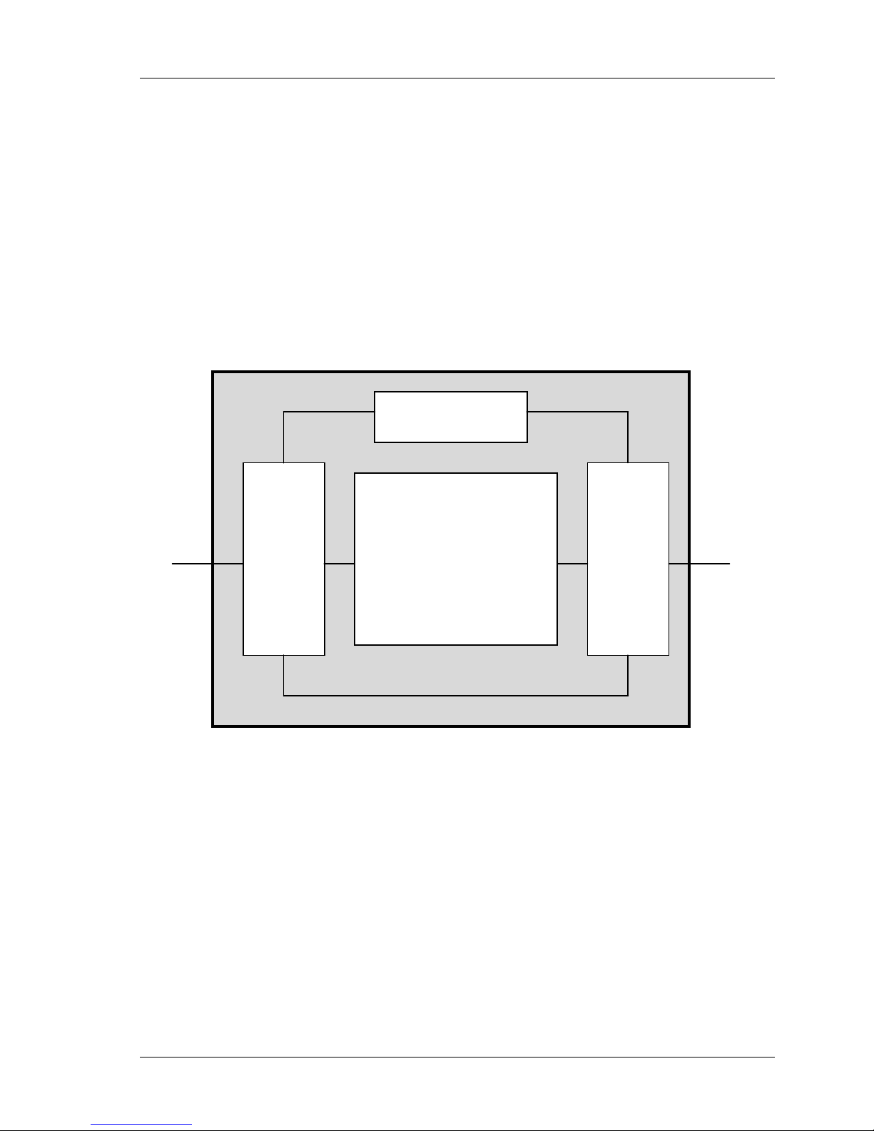
TVP4020 Programmers Reference Manual Overview
Bus
ce
Memory
I
e
VGA
Gra phics Hyperpipeline
2.2
2.2.1
Functional Overview
Memory Subsystem
ERMEDIA
P
provides flexible support for the memory subsystem (Fig. 2.1).
This allows the system designer a wide choice of price/performance
tradeoffs.
The same physical memory holds all data used by P
ERMEDIA
. Internally
the data types are divided into texture, localbuffer and framebuffer. The
localbuffer holds depth and stencil data; the framebuffer holds color data
for display.
Host Bus SGRAM
2.2.2
Host Interface
Conceptually P
Interfa
Bypass
Figure 2.1 External Interfaces
ERMEDIA
can be viewed as a register file. Control registers
nterfac
are primed with the information required for a primitive, and then to start
the chip drawing, a write is made to a Command register
ERMEDIA
P
registers can be accessed directly through the memory map.
Registers can be accessed either individually or in groups.
The chip also supports a bypass route to the memory to allow direct
read/write of pixels, and implementation of algorithms not directly
supported by P
ERMEDIA
.
3
Page 13
Overview TVP4020 Programmers Reference Manual
2.2.3
2.2.4
Task Switching
Where multiple applications wish to make simultaneous access to
ERMEDIA
P
the loading of correct state. P
, it is the responsibility of the software driving the chip to handle
ERMEDIA
has been designed to support a
number of different software architectures.
• Synchronous operation means that a new task can load its context
without waiting for current rendering to complete
• All loadable state can be read back
• A Sync command is provided to flush all rendering. This can be polled
or it can return an interrupt
SVGA
ERMEDIA
P
contains a fast VGA core. The P
ERMEDIA
SVGA is used for
DOS VGA applications and during boot time before switching to use the
Graphics Hyperpipeline. This document does not cover VGA
programming. Specific information on P
the
TVP4020 Hardware Reference Manual
ERMEDIA
’s VGA can be found in
. VGA information, such as
standard registers, is described in the “Programmer’s Guide to the EGA,
VGA and Super VGA Cards” by Richards F. Ferraro.
The following standard VGA modes are supported:
Mode
(hex)
00 0
0*
0+
01 1
1*
1+
02 2
2*
2+
03 3
3*
3+
04 4 40 by 25 8 by 8 4/256K 1 Graph 320 by 200
05 5 40 by 25 8 by 8 4/256K bw 1 Graph 320 by 200
06 6 80 by 25 8 by 8 2/256K bw 1 Graph 640 by 200
07 7
7+
0D D 40 by 25 8 by 8 16/256K 8 Graph 320 by 200
0E E 80 by 25 8 by 8 16/256K 4 Graph 640 by 200
0F F 80 by 25 8 by 14 bw 2 Graph 640 by 350
10 10 80 by 25 8 by 14 16/256K 2 Graph 640 by 350
11 11 80 by 30 8 by 16 2/256K 1 Graph 640 by 480
12 12 80 by 30 8 by 16 16/256K 1 Graph 640 by 480
13 13 40 by 25 8 by 8 256/256K 1 Graph 320 by 200
Alpha
Format
40 by 25
40 by 25
40 by 25
40 by 25
40 by 25
40 by 25
80 by 25
80 by 25
80 by 25
80 by 25
80 by 25
80 by 25
80 by 25
80 by 25
Char Size Colors Max
Page
8 by 8
8 by 14
9 by 16
8 by 8
8 by 14
9 by 16
8 by 8
8 by 14
9 by 16
8 by 8
8 by 14
9 by 16
9 by 14
9 by 16
16/256K bw
16/256K bw
16/256K bw
16/256K
16/256K
16/256K
16/256K bw
16/256K bw
16/256K bw
16/256K
16/256K
16/256K
bw
bw
8
8
8
8
8
8
8
8
8
8
8
8
8
8
Type
Format
Alpha
Alpha
Alpha
Alpha
Alpha
Alpha
Alpha
Alpha
Alpha
Alpha
Alpha
Alpha
Alpha
Alpha
Resolution
320 by 200
320 by 350
360 by 400
320 by 200
320 by 350
360 by 400
640 by 200
640 by 350
720 by 400
720 by 200
640 by 350
720 by 400
720 by 350
720 by 400
4
Table 2.1
Standard VGA Modes
Page 14

TVP4020 Programmers Reference Manual Overview
The following VESA SVGA modes are supported:
Mode (hex) Pixels Colors
100 640 by
400
101 640 by
480
Table 2.2 VESA SVGA Modes
256
256
ModeX is also supported.
5
Page 15

Programming Model TVP4020 Programmers Reference Manual
3.
Programming Model
This chapter describes the programming model for P
ERMEDIA
. It
describes the interface conceptually rather than detailing specific
registers and their exact usage. In-depth descriptions of how to program
ERMEDIA
P
ERMEDIA
P
Region Address Space Bytes Description Comments
Config Configuration 256 PCI Configuration PCI special
Zero Memory 128K Control Registers relocatable
One Memory 8M Memory Region One relocatable
Two Memory 8M Memory Region Two relocatable
ROM Memory 64K Expansion ROM relocatable
SVGA Memory & I/ O - SVGA Addr esses optional & fixed
Address Range Description Byte Swap
0000.0000 -> 0000.0FFF Control & Status No
0000.1000 -> 0000.1FFF Memory Control No
0000.2000 -> 0000.2FFF GP FIFO access No
0000.3000 -> 0000.3FFF Video Control No
0000.4000 -> 0000.4FFF RAMDAC No
0000.5000 -> 0000.57FF Video Str eam s General Purpose
0000.5800 -> 0000.5FFF Video Streams Control No
0000.6000 -> 0000.6FFF SVGA Control No
0000.7000 -> 0000.7FFF Reserved No
0000.8000 ->
0000.FFFF
0001.0000 -> 0001.0FFF Control & Status Yes
0001.1000 -> 0001.1FFF Memory Control Yes
0001.2000 -> 0001.2FFF GP FIFO access Yes
0001.3000 -> 0001.3FFF Video Control Yes
0001.4000 -> 0001.4FFF RAMDAC Yes
0001.5000 -> 0001.57FF Video Str eam s General Purpose
0001.5800 -> 0001.5FFF Video Streams Control No
0001.6000 -> 0001.6FFF SVGA Control Yes
0001.7000 -> 0001.7FFF Reserved Yes
for specific drawing operations can be found in later chapters.
is divided into the following memory regions:
Table 3.1 Memory Regions
No
Bus
GP Registers No
No
Bus
6
Page 16

TVP4020 Programmers Reference Manual Programming Model
3.1
0001.8000 ->
0001.FFFF
Table 3.2 Region 0 Address Map
ERMEDIA
P
as a Register file
The simplest way to view the interface to the P
Processor is as a flat block of memory-mapped registers (
file). This register file appears as part of the address map for P
When a P
ERMEDIA
host software driver is initialized it can map the
GP Registers Yes
ERMEDIA
Graphic
i.e.
a register
ERMEDIA
.
register file into its address space. Each register has an associated
address tag, giving its offset from the base of the register file (since all
registers reside on a 64-bit boundary, the tag offset is measured in
multiples of 8 bytes). The most straightforward way to load a value into a
register is to write the data to its mapped address. In reality the chip
interface comprises a 256 entry deep FIFO, and each write to a register
causes the written value and the register’s address tag to be written as a
new entry in the FIFO.
Programming P
ERMEDIA
to draw a primitive consists of writing values to
the appropriate registers followed by a write to a command register. This
last write triggers the start of drawing.
ERMEDIA
P
has approximately 200 registers. All registers are 32 bits wide
and should be 32-bit addressed. Many registers are split into bit fields,
and it should be noted that bit 0 is the least significant bit.
In future chip revisions the register file may be extended and currently
unused bits in certain registers may be assigned new meanings.
Software developers should ensure that only defined registers are
written to and that undefined bits in registers are always written as
zeros. The only exception to this rule is that in certain registers it is
convenient to allow unmasked values to be written to registers which
hold numeric data. These fields are marked as "not used" in Appendix A
and elsewhere.
Register Types
ERMEDIA
P
• Control Registers
• Command Registers
• Internal Registers
has three main types of register:
Control Registers are updated only by the host - the chip effectively uses
them as read-only registers. Examples of control registers are the
scissor clip min and max registers. Once initialized by the host, the chip
7
Page 17

Programming Model TVP4020 Programmers Reference Manual
only reads these registers to determine the scissor clip extents. Most
registers are control registers.
Command Registers are those which, when written to, cause some
action to occur. Typically, the host will initialize the appropriate control
registers and then write to a command register to initiate drawing. Some
command registers such as ResetPickResult or Sync do not initiate
rendering. Apart from these, there are two types of command registers:
begin-draw and continue-draw. Begin-draw commands cause rendering
to start with those values specified by the control registers. Continuedraw commands cause drawing to continue with internal register values
as they were when the previous drawing operation completed. Making
use of continue-draw commands can significantly reduce the amount of
data that has to be loaded into P
ERMEDIA
when drawing multiple
connected objects such as polylines. Examples of command registers
include the Render and ContinueNewLine registers.
For convenience in this document we often refer to "sending a Render
command to P
ERMEDIA
" rather than saying "the Render Command
register is written to, which initiates drawing" .
Internal Registers are not accessible to host software. They are used
internally by the chip to keep track of changing values. Some control
registers have corresponding internal registers. When a begin-draw
command is sent and before rendering starts, the internal registers are
updated with the values in the corresponding control registers. If a
continue-draw command is sent then this update does not happen and
drawing continues with the current values in the internal registers. For
example, if a line is being drawn then the StartXDom and StartY control
registers specify the (x, y) coordinates of the first point in the line. When
a begin-draw command is sent these values are copied into internal
registers. As the line drawing progresses these internal registers are
updated to contain the (x, y) coordinates of the pixel being drawn. When
drawing has completed the internal registers contain the (x, y)
coordinates of the next point that would have been drawn. If a continuedraw command is now given, these final (x, y) internal values are not
modified and further drawing uses these values. If a begin-draw
command had been used the internal registers would have been reloaded from the StartXDom and StartY registers.
For the most part internal registers can be ignored. It is helpful to
appreciate that they exist in order to understand the continue-draw
commands.
Efficiency Issues and Register Types
Software developers wishing to write device drivers for P
become familiar with the different type s of registers. Some control
registers such as the StartXDom and StartY registers have to be
8
ERMEDIA
should
Page 18

TVP4020 Programmers Reference Manual Programming Model
updated for almost every primitive whereas other control registers such
as those for scissor clip or logical ops can be updated much less
frequently. Pre-loading of the appropriate control registers can reduce
the amount of data that has to be loaded into the chip for a given
primitive thus improving efficiency. In addition, as described above, the
final values in internal registers can sometimes be used for subsequent
drawing operations.
The tables in Appendix D lists the graphics registers according to their
type, name and address.
3.2
3.2.1
ERMEDIA
P
There are four ways of loading P
• The host writes a value to the mapped address of the register
• The host writes address-tag/data pairs to the FIFO.
• The host writes address-tag/data pairs to the FIFO via DMA.
• The host writes to raw memory mapped GP FIFO addresses.
I/O Interface
ERMEDIA
registers:
In cases where the host writes data values directly to the chip via the
register file, consideration has to be given to FIFO overflow (unless PCI
Disconnect is enabled). The InFIFOSpace register indicates how many
free entries remain in the FIFO. Before writing to any register, the host
must ensure that there is enough space left in the FIFO. The values in
this register can be read at any time. When using DMA, the DMA
controller will automatically e nsure that there is room in the FIFO befo re
it performs further transfers. Thus a buffer of any size up to 64K, 32 bit
words, can be passed to the DMA controller. The FIFO and DMA
controller are described in more detail below.
PCI Disconnect
The PCI bus protocol incorporates a feature known as PCI Disconnect,
which is supported by P
ERMEDIA
. PCI Disconnect is enabled by writing a
one to bit zero of the DisconnectControl register which is at offset 0x68
in PCI Region 0. Once the P
ERMEDIA
is in this mode, if the host processor
attempts to write to the full FIFO then instead of the write being lost, the
ERMEDIA
P
chip will assert PCI Disconnect which will cause the host
processor to keep retrying the write cycle until it succeeds.
This feature allows faster download of data to P
need not poll the InFIFOSpace register but should be used with care
since whenever the PCI Disconnect is asserted the bus is effectively
hogged by the host processor until such time as the P
an entry in its FIFO. In general this mode should only be used either for
operations where it is known that the P
ERMEDIA
ERMEDIA
, since the host
ERMEDIA
frees up
can consume data faster
9
Page 19

Programming Model TVP4020 Programmers Reference Manual
than the host can generate it, or where there are no time critical
peripherals sharing the PCI bus.
3.2.2
3.2.3
Idle bit
In some systems, PCI Disconnect may cause interrupts to be lost if it
used too often or for too long. It is normal to only rely on this feature
when it is known that the data to be sent to P
ERMEDIA
will be absorbed
quickly enough that the disconnect will seldom be used. It also advisable
to check that the Graphics Processor is not processing a large primitive
before transferring data of this sort, and this may be done by checking
the Graphics Processor Active bit in the PCI Disconnect register.
Disconnect should not normally be enabled if this bit is set.
FIFO ControlFIFO Control
The description in section §3.1 above considered the P
ERMEDIA
to be a register file. More precisely, when a data value is written to a
register, this value and the address tag for that register are combined
and put into the FIFO as a new entry. The actual register is not updated
until P
ERMEDIA
processes this entry. In the case where P
performing a time consuming operation (
e.g.
drawing a large texture
ERMEDIA
mapped polygon), and not draining the FIFO very quickly, it is possible
for the FIFO to become full. If a write to a register is performed when the
FIFO is full no entry is put into the FIFO and that write is effectively lost.
interface
is busy
The input FIFO is 256 entries deep and each entry consists of a tag/data
pair; an address word which addresses the register to be updated,
followed by the data to be sent to the register. The InFIFOSpace register
can be read to determine how many entries are free. The value returned
by this register will never be greater than 256.
An example of loading P
ERMEDIA
registers using the FIFO is given below.
The pseudocode fills a series of rectangles. Details of the conventions
used in the pseudocode examples may be found in Appendix B.
Assume that the data to draw a single rectangle consists of 5 words
(including the Render command).
dXDom(0x0); // common set-up
dXSub(0x0);
dY(1);
for (i = 0; i < nrects; ++i) {
while (*InFIFOSpace < 5)
; // wait for room
StartXDom (rect->x1);
StartXSub (rect->x2);
Count (rect->y2 - rect->y1);
YStart(rect->y1);
10
Page 20

TVP4020 Programmers Reference Manual Programming Model
Render (PERMEDIA_TRAPEZOID_PRIMITIVE);
}
The InFIFOSpace FIFO control register contains a count of the number
of entries currently free in the FIFO. The chip increments this register for
each entry it removes from the FIFO and decrements it every time the
host puts an entry in the FIFO. Before writing to the input FIFO, the user
must check that there is sufficient space by reading the InFIFOSpace
register.
The Graphics Core FIFO interface provides a port through which both
GC register addresses and data can be sent to the input FIFO. A range
of 4 Kbytes of host space is provided although all data may be sent
through one address in the range. ALL accesses go directly to the FIFO;
the range is provided to allow for data transfer schemes which force the
use of incrementing addresses.
Note that the GC registers cannot be read through this interface.
Command buffers generated to be sent to the input FIFO interface, may
be read directly by P
ERMEDIA
by using the DMA controller.
3.2.4
A data formatting scheme is provided to allow for multiple data words to
be sent with one address word where adjacent or grouped registers are
being written, or where one register is to be written many times.
Note. The FIFO interface can be accessed at 32 bit boundaries. This is
to allow a direct copy from a DMA format buffer.
The DMA Interface
Loading registers directly via the FIFO is often an inefficient way to
download data to P
a small number of entries, P
ERMEDIA
. Given that the FIFO can accommodate only
ERMEDIA
has to be frequently interrogated to
determine how much space is left. Also, consider the situation where a
given API function requires a large amount of data to be sent to
ERMEDIA
P
. If the FIFO is written directly then a return from this function is
not possible until almost all the data has been consumed by P
This may take some time depending on the types of primitives being
drawn.
To avoid these problems P
ERMEDIA
provides an on-chip DMA controller
which can be used to load data from arbitrary sized (< 64K 32-bit words)
host buffers into the FIFO. In its simplest form the host software has to
prepare a host buffer containing register address tag descriptions and
data values. It then writes the base address of this buffer to the
DMAAddress register and the count of the number of words to transfer
to the DMACount register. Writing to the DMACount register starts the
DMA transfer and the host can now perform other work. In general, if the
complete set of rendering commands required by a given call to a driver
ERMEDIA
.
11
Page 21

Programming Model TVP4020 Programmers Reference Manual
function can be loaded into a single DMA buffer then the driver function
can return. Meanwhile, in parallel, P
ERMEDIA
is reading data from the
host buffer and loading it into its FIFO. FIFO overflow never occurs since
the DMA controller automatically waits until there is room in the FIFO
before doing any transfers.
The only restriction on the use of DMA control registers is that before
attempting to reload the DMACount register the host software must wait
until previous DMA has completed. It is valid to load the DMAAddress
register while the previous DMA is in progress since the address is
latched internally at the start of the DMA transfer. Many display driver
functions can be implemented using the following skeleton structure:
do any pre-work
DMAAddress(address of dma_buffer);
while (TRUE) {
count = *DMACount; // note this is volatile
if (count) {
while (--count)
; // wait for count to expire
}
else
break; // DMA completed
}
copy render data into DMA buffer
DMACount(number of words in DMA buffer)
return
12
Using DMA leaves the host free to return to the application, while in
parallel, P
ERMEDIA
is performing the DMA and drawing. This can increase
performance significantly over loading a FIFO directly. In addition, some
algorithms require that data be loaded multiple times (e.g. drawing the
same object across multiple clipping rectangles). Since the P
ERMEDIA
DMA only reads the buffer data, it can be downloaded many times
simply by restarting the DMA. This can be very beneficial if composing
the buffer data is a time consuming task.
A further optimization is to use a double buffered mechanism with two
DMA buffers. This allows the second buffer to be filled before waiting for
the previous DMA to complete thus further improving the parallelism
between host and P
ERMEDIA
processing.
Page 22
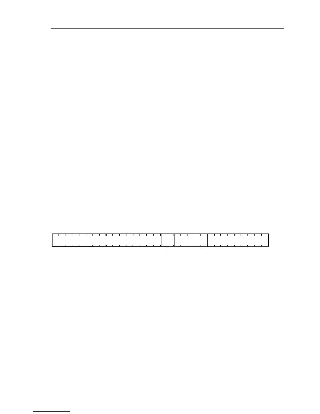
TVP4020 Programmers Reference Manual Programming Model
08162431
Cou n t or Ma sk
Addres s Tag
res erved
Mode
0 = Hold tag
1 = Increment tag
2 = Indexed ta g
3 = Reser ve d
do any pre-work
get free DMA buffer and mark as in use
put render data into this new buffer
DMAAddress(address of new buffer)
while (TRUE) {
count = *DMACount; // note this is volatile
if (count) {
while (--count)
; // wait for count to expire
}
else
break; // DMA completed
}
DMACount(number of words in new buffer)
mark the old buffer as free
return
In general the DMA buffer format consists of a 32-bit address tag
description word followed by one or more data words. The DMA buffer
consists of one or more sets of these formats. The following paragraphs
describe the different types of tag description words that can be used.
DMA Tag Description Format
When DMA is performed each 32-bit tag description in the DMA buffer
conforms to the following format.
res erved
Figure 3.1
DMA Tag Description Format
There are 3 different tag addressing modes for DMA: hold, increment
and indexed. The different DMA modes are provided to reduce the
amount of data which needs to be transferred, hence making better use
of the available DMA bandwidth. Each of these is described in the
following sections. Each row in the following diagrams represents a 32bit value in the DMA buffer. The address tag for each register is given in
the Graphics Register Reference Appendix D.
Hold Format
13
Page 23

Programming Model TVP4020 Programmers Reference Manual
address-tag with Count=n-1, Mode=0
value 1
...
value n
This is commonly used for image download by setting the
SyncOnHostData bit in the Render command.. In this format the 32-bit
tag description contains a tag value and a count specifying the number
of data words following in the buffer. The DMA controller writes each of
the data words to the same address tag. For example, this is useful for
image download where pixel data is continuously written to the Color
register. The bottom 9 bits specify the register to which the data should
be written; the high-order 16 bits specify the number of data words
(minus 1) which follow in the buffer and which should be written to the
address tag (note that the 2-bit mode field for this format is zero so a
given tag value can simply be loaded into the low order 16 bits).
A special case of this format is where the top 16 bits are zero indicating
that a single data value follows the tag (
i.e.
the 32-bit tag description is
simply the address tag value itself). This allows simple DMA buffers to
be constructed which consist of tag/data pairs. For example to render a
horizontal span 10 pixels long starting from (2,5) the DMA buffer could
look like this:
StartXDom
2 << 16
StartY
5 << 16
StartXSub12 << 16
Count
1
Render
(trapezoid render command)
Increment Format
address-tag with Count=n-1, Mode=1
value 1
...
value n
This format is similar to the hold format except that as each data value is
loaded the address tag is incremented (the value in the DMA buffer is
not changed; P
allows contiguous P
ERMEDIA
ERMEDIA
updates an internal copy). Thus, this mode
registers to be loaded by specifying a single
32-bit tag value followed by a data word for each register. The low-order
9 bits specify the address tag of the first register to be loaded. The 2 bit
mode field is set to 1 and the high-order 16 bits are set to the count
14
Page 24

TVP4020 Programmers Reference Manual Programming Model
(minus 1) of the number of registers to update. To enable use of this
format, the P
ERMEDIA
register file has been organized so that registers
which are frequently loaded together have adjacent address tags. For
example, the 8 AreaStipplePattern registers can be loaded as follows:
AreaStipplePattern0, Count=7, Mode=1
row 0 bits
row 1 bits
...
row 7 bits
Indexed Format
ERMEDIA
P
address tags are 9 bit values. For the purposes of the Indexed
DMA Format they are organized into major groups and within each
group there are up to 16 tags. The low-order 4 bits of a tag give its offset
within the group. The high-order 5 bits give the major group number.
Appendix D Register Table, lists the individual registers with their Major
Group and Offset.
8
Major Group Offset
Figure 3.2
Indexed Format
094
This format allows up to 16 registers within a group to be loaded while
still only specifying a single address tag description word.
address tag with Mask, Mode=2
value 1
...
value n
If the Mode of the address tag description word is set to indexed mode
then the high-order 16 bits are used as a mask to indicate which
registers within the group are to be used. The bottom 4 bits of the
address tag description word are unused. The group is specified by bits
4 to 8. Each bit in the mask is used to represent a unique tag within the
group. If a bit is set then the corresponding register will be loaded. The
number of bits set in the mask determines the number of data words that
should be following the tag description word in the DMA buffer. The data
is stored in order of increasing corresponding address tag. For example,
15
Page 25

Programming Model TVP4020 Programmers Reference Manual
0x003280F0
value 1
value 2
value 3
The Mode bits are set to 2 so this is indexed mode. The Mask field
(0x0032) has 3 bits set so there are three data words following the tag
description word. Bits 1, 4 and 5 are set so the tag offsets are 1, 4 and 5.
The major group is given by the bits 4-8 which are 0x0F (in indexed
mode bits 0-3 are ignored). Thus the actual registers to update have
address tags 0x0F1, 0x0F4 and 0x0F5. These are updated with value 1,
value 2 and value 3 respectively.
DMA Example
The following pseudo-code shows the previous example of drawing a
series of rectangles but this time using the DMA controller. This example
uses a single DMA buffer and the simplest Hold Mode for the tag
description words in the buffer.
UINT32 *pbuf;
DMAAddress (physical address of dma_buffer)
while (*DMACount != 0)
; // wait for DMA to complete
pbuf = dma_buffer;
*pbuf++ = PERMEDIATagdXDom;
*pbuf++ = 0;
*pbuf++ = PERMEDIATagdXSub;
*pbuf++ = 0;
*pbuf++ = PERMEDIATagdY;
*pbuf++ = 1 << 16;
for (i = 0; i < nrects; ++i) {
*pbuf++ = PERMEDIATagStartXDom;
*pbuf++ = rect->x1 << 16; // Start dominant edge
*pbuf++ = PERMEDIATagStartXSub
*pbuf++ = rect->x2 << 16; // Start of subordinate edge
*pbuf++ = PERMEDIATagCount;
*pbuf++ = rect->y2 - rect->y1;
*pbuf++ = PERMEDIATagYStart;
*pbuf++ = rect->y1 << 16;
*pbuf++ = PERMEDIATagRender;
*pbuf++ = PERMEDIA_TRAPEZOID_PRIMITIVE;
}
// initiate DMA
DMACount((int)(pbuf - dma_buffer))
16
Page 26

TVP4020 Programmers Reference Manual Programming Model
The example assumes that a host buffer has been previously allocated
and is pointed at by “dma_buffer”. It is worth noting that significantly
less data would be required if indexed tags were used in this example.
DMA Buffer Addresses
Host software must generate the correct DMA buffer address for the
ERMEDIA
P
to P
DMA controller. Normally, this means that the address passed
ERMEDIA
must be the physical address of the DMA buffer in host
memory. The buffer must also reside at contiguous physical addresses
as accessed by P
ERMEDIA
. On a system which uses virtual memory for
the address space of a task, some method of allocating contiguous
physical memory, and mapping this into the address space of a task,
must be used.
If the virtual memory buffer maps to non-contiguous physical memory
then the buffer must be divided into sets of contiguous physical memory
pages and each of these sets transferred separately. In such a situation
the whole DMA buffer cannot be transferred in one go; the host software
must wait for each set to be transferred. Often the best way to handle
these fragmented transfers is via an interrupt handler.
DMA Interrupts
ERMEDIA
P
provides interrupt support, as an alternative means of
determining when a DMA transfer is complete. This can provide
considerable speed advantage. If enabled, the interrupt is generated
whenever the DMACount register changes from having a non-zero to
having a zero value. Since the DMACount register is decremented every
time a data item is transferred from the DMA buffer this happens when
the last data item is transferred from the DMA buffer.
To enable the DMA interrupt, the DMAInterruptEnable bit must be set in
the IntEnable register. The interrupt handler should check the DMAFlag
bit in the IntFlags register to determine that a DMA interrupt has actually
occurred. To clear the interrupt a word should be written to the IntFlags
register with the DMAFlag bit set to one.
A typical use of DMA interrupts might be as follows:
prepare DMA buffer
DMACount(n); // start a DMA transfer
prepare next DMA buffer
while (*DMACount != 0) {
mask interrupts
set DMA Interrupt Enable bit in IntEnable register
sleep on interrupt handler wake up
unmask interrupts
}
DMACount(n) // start the next DMA sequence
17
Page 27

Programming Model TVP4020 Programmers Reference Manual
The interrupt handler could then be
if (*IntFlags & DMA Flag bit) {
reset DMA Flag bit in IntFlags
send wake up to main task
}
Interrupts are complicated and depend on the facilities provided by the
host operating system. The above pseudocode only hints at the system
details.
This scheme frees the processor for other work while DMA is being
completed. Since the overhead of handling an interrupt is often quite
high for the host processor, the scheme should be tuned to allow a
period of polling before sleeping on the interrupt.
3.2.5
Output FIFO and Graphics Processor FIFO Interface
To read data back from P
ERMEDIA
an output FIFO is provided. Each entry
in this FIFO is 32-bits wide and it can hold tag or data values. Thus its
format is unlike the input FIFO whose entries are always tag/data pairs
(we can think of each entry in the input FIFO as being 41 bits wide – 9
bits for the tag and 32 bits for the data). The type of data written by
ERMEDIA
P
to the output FIFO is controlled by the FilterMode register. This
register allows filtering of output data in various categories including the
following:
• Depth: output in this category results from an image upload of the
Depth buffer.
• Stencil: output in this category results from an image upload of the
Stencil buffer.
• Color: output in this category results from an image upload of the
framebuffer.
• Synchronization: synchronization data is sent in response to a Sync
command.
The data for the FilterMode register consists of 2 bits per category. If the
least significant of these two bits is set (0x1) then output of the register
tag for that category is enabled; if the most significant bit is set (0x2)
then output of the data for that category is enabled. Both tag and data
output can be enabled at the same time. In this case the tag is written
first to the FIFO followed by the data. The FilterMode register is
described in more detail in section §5.15.
For example, to perform an image upload from the framebuffer, the
FilterMode register should have data output enabled for the Color
category. Then, the rectangular area to be uploaded should be
described to the Rasterizer. Each pixel that is read from the framebuffer
will then be placed into the output FIFO. If the output FIFO becomes full,
18
Page 28

TVP4020 Programmers Reference Manual Programming Model
then P
ERMEDIA
will block internally until space becomes available. It is
the programmer’s responsibility to read all data from the output FIFO.
For example, it is important to know how many pixels should result from
an image upload and to read exactly this many from the FIFO.
To read data from the output FIFO the OutputFIFOWords register should
first be read to determine the number of entries in the FIFO (reading
from the FIFO when it is empty returns undefined data). Then this many
32-bit data items are read from the FIFO. This procedure is repeated
until all the expected data or tag items have been read. The address of
the output FIFO is described below.
NB all expected data must be read back. P
ERMEDIA
will block if the output
FIFO becomes full. Programmers must be careful to avoid the deadlock
condition that will result if the host is waiting for space to become free in
the input FIFO while P
ERMEDIA
is waiting for the host to read data from
the output FIFO.
Graphics Processor FIFO Interface
ERMEDIA
P
has a sequence of 1K x 32 bit addresses in the PCI Region 0
address map called the Graphics Processor FIFO Interface. To read
from the output FIFO any address in this range can be read (normally a
program will choose the first address and use this as the address for the
output FIFO). All 32-bit addresses in this region perform the same
function – the range of addresses is provided for data transfer schemes
which force the use of incrementing addresses.
Writing to a location in this address range provides raw access to the
input FIFO. Again, the first address is normally chosen. Thus the same
address can be used for both input and output FIFOs. Reading gives
access to the output FIFO; writing gives access to the input FIFO.
Writing to the input FIFO by this method is different from writing to the
memory mapped register file. Since the register file has a unique
address for each register, writing to this unique address allows P
ERMEDIA
to determine the register for which the write is intended. This allows a
tag/data pair to be constructed and inserted into the input FIFO. When
writing to the raw FIFO address an address tag description must first be
written followed by the associated data. In fact, the format of the tag
descriptions and the data that follows is identical to that described above
for DMA buffers. Instead of using the P
transfer data to P
ERMEDIA
by constructing a DMA-style buffer of data and
ERMEDIA
DMA it is possible to
then copying each item in this buffer to the raw input FIFO address.
Based on the tag descriptions and data written P
ERMEDIA
constructs
tag/data pairs to enter as real FIFO entries. The DMA mechanism can
be thought of as an automatic way of writing to the raw input FIFO
address.
19
Page 29

Programming Model TVP4020 Programmers Reference Manual
Note, that when writing to the raw FIFO address the FIFO full condition
must still be checked by reading the InFIFOSpace register. However,
writing tag descriptions does not cause any entries to be entered into the
FIFO – such a write simply establishes a set of tags to be paired with the
subsequent data. Thus, free space need be ensured only for actual data
items that are written (not the tag values). For example, in the simplest
case where each tag is followed by a single data item, assuming that the
FIFO is empty, then 32 writes are possible before checking again for
free space.
3.3
3.4
See the
TVP4020 Hardware Reference Manual
for more details of the
Graphics Processor FIFO Interface address range.
Interrupts
All interrupts can be individually enabled and disabled. Refer to the
TVP4020 Hardware Reference Manual
Synchronization
for more details.
There are two main cases where the host must synchronize with
ERMEDIA
P
• before reading back from P
• before directly accessing the memory via the bypass mechanism
Also the host must synchronize with P
:
ERMEDIA
registers
ERMEDIA for
framebuffer
management tasks such as double buffering, though this may be better
handled using the SuspendUntilFrameBlank command. Synchronizing
with P
ERMEDIA
implies waiting for any pending DMA to complete and
waiting for the chip to complete any processing currently being
performed. The following pseudo-code shows the general scheme:
20
Page 30

TVP4020 Programmers Reference Manual Programming Model
PERMEDIAData data;
// wait for DMA to complete
while (*DMACount != 0) {
poll or wait for interrupt
}
while (*InFIFOSpace < 2) {
; // wait for free space in the FIFO
}
// enable sync output and send the Sync command
data.Word = 0;
data.FilterMode.Synchronization = 0x1;
FilterMode(data.Word);
Sync(0x0);
/* wait for the sync output data */
do {
while (*OutFIFOWords == 0)
; // poll waiting for data in output FIFO
} while (*OutputFIFO != Sync_tag);
3.5
Initially, we wait for DMA to complete as normal. We then have to wait
for space to become free in the FIFO (since the DMA controller actually
loads the FIFO). We need space for 2 registers: one to enable
generation of an output sync value, and the Sync command itself. The
enable flag can be set at initialization time. The output value will be
generated only when a Sync command has actually been sent, and
ERMEDIA
P
has then completed all processing.
Rather than polling, it is possible to use a Sync interrupt as mentioned in
the previous section. As well as enabling the interrupt and setting the
filter mode, the data sent in the Sync command must have the most
significant bit set in order to generate the interrupt. The interrupt is
generated when the tag or data reaches the output end of the Host Out
FIFO. Use of the Sync interrupt has to be considered carefully as
ERMEDIA
P
will generally empty the FIFO more quickly than it takes to set-
up and handle the interrupt.
Host Memory Bypass
Normally, the host will access memory indirectly via commands sent to
the P
ERMEDIA
FIFO interface. However, P
ERMEDIA
does provide the whole
memory as part of its address space so that it can be memory mapped
by an application. Access to the memory via this route is independent of
ERMEDIA
the P
FIFO.
21
Page 31

Programming Model TVP4020 Programmers Reference Manual
Drivers may choose to use direct access to memory for algorithms which
are not supported by P
ERMEDIA
or for better performance in some
specific cases. This may be so, for example, when multiple pixels can be
written simultaneously and there is minimal host software overhead.
A driver making use of the bypass mechanism should synchronize
memory accesses made through the FIFO with those made directly
through the memory map. If data is written to the FIFO and then an
access is made to the memory, it is possible that the memory access will
occur before the commands in the FIFO have been fully processed. This
lack of temporal ordering is generally undesirable.
There are two windows through which the memory can be accessed.
Each window can have its own data formatting control that allows for
different forms of byte swapping and data packing. If the framebuffer is
set to use the 5:5:5:1Front and 5:5:5:1Back color modes, two pixels are
packed into each 32 bit word, but each pixel belongs to a different buffer.
Adjacent pixels in the same buffer are separated by 16 bits. As some
software has difficulty with pixels that are not packed together, the
memory windows can be configured to remap the data so that only the
front or back buffer is visible, and it appears packed.
3.6
3.7
DMA Controller
A DMA controller is provided to allow transfer of data from the PCI bus to
ERMEDIA
P
memory. This controller is independent of the DMA controller
which feeds the Graphics Processor FIFO, and has support for
rectangular data structures and data formatting.
Register Read back
Under some operating environments, multiple tasks will want access to
ERMEDIA
the P
arbitrate access to P
circumstances, the state of the P
restored on each context switch. To facilitate this, the P
chip. Sometimes a server task or driver will want to
ERMEDIA
on behalf of multiple applications. In these
ERMEDIA
chip may need to be saved and
ERMEDIA
registers
can be read back. For details of which registers are readable, see
Appendix D Register Tables. Internal and command registers cannot be
read back.
To perform a context switch the host must first synchronize with
ERMEDIA
P
. This means sending a Sync command and waiting for the
sync output data to appear in the output FIFO. After this the registers
can be read back.
22
Page 32

TVP4020 Programmers Reference Manual Programming Model
3.8
To read a P
would be used for a write,
ERMEDIA
register the host reads the same address which
i.e.
the base address of the register file plus
the offset value for the register.
Note that since internal registers cannot be read back care must be
taken when context switching a task which is making use of continuedraw commands. Continue-draw commands rely on the internal registers
maintaining previous state. This state will be destroyed by any rendering
work done by a new task. To prevent this, continue-draw commands
should be performed via DMA since the context switch code has to wait
for outstanding DMA to complete. Alternatively, continue-draw
commands can be performed in a non-preemptable code segment.
Normally, reading back individual registers should be avoided. The need
to synchronize with the chip can adversely affect performance. It is
usually more appropriate to keep a software copy of the register which is
updated whenever the actual register is changed.
Byte Swapping
Internally P
ERMEDIA
operates in little-endian mode. However, P
ERMEDIA
is
designed to work with both big - and little-endian host processors. Since
the PCI Bus specification defines that byte ordering is preserved
regardless of the size of the transfer operation, P
facilities to handle byte swapping. See the
Reference Manual
for more details of byte-swapping via the PCI bus.
TVP4020 Hardware
ERMEDIA
provides
3.9
Additional support is provided within the graphics core of the chip to byte
swap images and bitmasks as they are transferred to and from the host.
These are documented in the relevant sections of chapter §5.
Red and Blue Swapping
For a given graphics board the RAMDAC and/or API will usually force a
given interpretation for true color pixel values. For example, 32-bit pixels
will be interpreted as either RGB (red at byte 2, green at byte 1 and blue
at byte 0) or BGR (blue at byte 2 and red at byte 0). The byte position for
red and blue may be important for software which has been written to
expect one byte order or the other, in particular when handling image
data stored in a file.
ERMEDIA
P
provides three registers to specify the byte positions of blue
and red internally. In the Texture/Fog/Blend unit the AlphaBlendMode
register contains a 1-bit field called ColorOrder. If this bit is set to zero
then the byte ordering is BGR; if the bit is set to one then the ordering is
RGB. As well as setting this bit in the Alpha Blend unit, it must also be
23
Page 33

Programming Model TVP4020 Programmers Reference Manual
set in the Color Format unit and the Texture Read unit via the
DitherMode and TextureDataFormat registers.
24
Page 34

TVP4020 Programmers Reference Manual
Memory I/O and Organiza tion
4.
4.1
Memory I/O and Organization
This section describes the arrangement of data stored in memory.
Although P
reference, this is divided into three buffers: the localbuffer, framebuffer
and texture buffer. Any of these buffers can be any size at any position
in the memory.
For 3D operation, associated with the framebuffer there would normally
be a localbuffer to hold depth and/or stencil information. A texture buffer
may be present if needed. For 2D operation the localbuffer would not
generally be used, but the texture buffer may be used to store pixmaps.
Patched Data
ERMEDIA
P
“patching”. Data is normally stored linearly in memory such that
incrementing addresses move from left to right along a scanline of the
appropriate buffer. The type of memory supported by P
page structure which allows fast accesses within a 2 Kbyte region, but
imposes a penalty for moving to a new 2 Kbyte region. This page
structure favors access patterns that move along a scanline but is
inefficient for moving vertically as the large change in address may
cause a page break.
ERMEDIA
supports an optional scheme for organizing memory, known as
has a single unified memory space for ease of
ERMEDIA
uses a
4.2
Patched data is organized so that there is less penalty for moving
vertically in a buffer at the expense of a decrease in performance for
moving horizontally. This is done by organizing memory such that a two
dimensional region or patch in the buffer corresponds to a linear
sequence in memory. A buffer will comprise lots of patches.
Two patch modes are supported which differ in the detail of how the data
is organized within the patch. Normal patch mode is used for localbuffer
and framebuffer data. Subpatch mode is used for texture and
framebuffer data. Patched data cannot be displayed, so patching of
framebuffer data is normally only done for off-screen bitmaps or when
processing localbuffer or texture data through the framebuffer units.
Localbuffer
The localbuffer holds the Depth and Stencil information corresponding to
each displayed pixel. The Depth field can be either 15 or 16 bits wide
and the Stencil field either 1 or 0 bits wide. The total width of the
25
Page 35

Memory I/O and Organiza tion
localbuffer data cannot be greater than 16 bits. If a Stencil field is
defined then it occupies bit 15; the depth field always starts at bit 0.
The format of the localbuffer is specified in two places: the
LBReadFormat register and the LBWriteFormat register.
TVP4020 Programmers Reference Manual
4.2.1
Localbuffer Coordinates
The translation from the internal coordinate system to the external
address map involves setting the base address of the window (or screen
if coordinates are screen relative) and positioning the origin in either the
top left or bottom left corner. The origin is specified in the LBReadMode
register.
The actual equations used to calculate the localbuffer address to read
and write are:
Bottom left origin
Destination address = LBWindowBase - Y * W + X
Source address = LBWindowBase - Y * W + X + LBSourceOffset
Top left origin
Destination address = LBWindowBase + Y * W + X
Source address = LBWindowBase + Y * W + X + LBSourceOffset
where:
X is the pixel's X coordinate.
Y is the pixel's Y coordinate.
26
LBWindowBase holds the base address in the localbuffer of the
current window.
LBSourceOffset is normally zero except during a copy operation
where data is read from one address and
written to another address. The offset between
source and destination is held in the
LBSourceOffset register.
W is the screen width. Only a subset of widths are
supported and these are encoded into the PP0,
PP1 and PP2 fields in the LBReadModeregister.
See the table in Appendix C for more details.
This produces the localbuffer address in pixels. For P
ERMEDIA
, the
localbuffer data is always 16 bits so the physical byte address is two
times the pixel address. The destination address is the address that data
will be written to; data may also be read from this address if read-modifywrite operations are needed such as depth testing. The source address
is mainly used for copy operations and is only used for reading data.
Page 36

TVP4020 Programmers Reference Manual
Memory I/O and Organiza tion
4.3
4.3.1
Framebuffer
The framebuffer holds color data produced by P
ERMEDIA
. The
framebuffer may hold both displayed and non-displayed data. Color
buffers can be placed anywhere in memory, there is no restriction on
areas that can be displayed from.
There may be several buffers, such as the front and back buffers of a
double buffered system, or the left and right buffers of a stereo system.
No restrictions are placed on the number or organization of the buffers
other than the total amount of memory fitted.
To access alternative buffers either the FBPixelOffset register can be
loaded, or the base address of the window held in the FBWindowBase
register can be redefined.
Framebuffer Coordinates
Coordinate generation for the framebuffer is similar to that for the
localbuffer except for the addition of FBPixelOffset. The WindowOrigin
bit in the FBReadMode register selects top left or bottom left as the
origin for the framebuffer.
The actual equations used to calculate the framebuffer address to read
and write are:
Bottom left origin
Destination address = FBWindowBase - Y * W + X + FBPixelOffset
Source address = FBWindowBase - Y * W + X + FBPixelOffset + FBSourceOffset
Top left origin
Destination address = FBWindowBase + Y * W + X + FBPixelOffset
Source address = FBWindowBase + Y * W + X + FBPixelOffset + FBSourceOffset
where:
X is the pixel's X coordinate,
Y is the pixel's Y coordinate,
FBWindowBase holds the base address in the framebuffer of the
current window.
FBPixelOffset is normally zero except when multi-buffer writes
are needed when it gives a way to access pixels
in alternative buffers without changing the
FBWindowBase register. This is useful as the
window system may be asynchronously
changing the window's position on the screen. It
is held in the FBPixelOffset register.
27
Page 37

Memory I/O and Organiza tion
FBSourceOffsetis normally zero except during a copy operation
W is the screen width. Only a subset of widths are
These address calculations translate a 2D address into a linear address
so non power of two framebuffer widths (e.g. 640) are economical in
memory. The address is in pixels; this is translated to a physical byte
address by multiplying by the number of bytes in the pixel.
The width is specified as the sum of selected partial products which are
selected by the fields PP0, PP1 and PP2 in the FBReadMode register.
This is the same mechanism as is used to set the width of the
localbuffer, however the widths may be set independently. The range of
widths supported are tabulated in Appendix C, together with the values
for each of the PP fields. This table holds all the common screen widths.
TVP4020 Programmers Reference Manual
where data is read from one address and
written to another address. The FBSourceOffset
is held in the FBSourceOffset register.
supported and these are encoded into the PP0,
PP1 and PP2 fields in the FBReadMode
register. See the table in Appendix C for more
details.
4.3.2
For arbitrary screen sizes, for instance when rendering to 'off screen'
memory such as bitmaps the next largest width from the table must be
chosen. The difference between the table width and the bitmap width will
be an unused strip of pixels down the right hand side of the bitmap.
Note that such bitmaps can be copied to the screen only as a series of
scanlines rather than as a rectangular block, unless the Texture Read
unit is used. In this case the stride for the read can be set differently to
the write by means of the partial products However, windowing systems
often store offscreen bitmaps in rectangular regions which use the same
stride as the screen. In this case normal bitblts can be used
Framebuffer Color Formats
The contents of the framebuffer can be regarded in two ways:
•
As a collection of fields of up to 32 bits with no meaning or assumed
format as far as P
ERMEDIA
is concerned. Bit planes may be allocated
to control cursor, color look u p tables (LUTs), multi-buffer visibility or
priority functions. In this case P
ERMEDIA
will be used to set and clear
bit planes quickly but not perform any color processing such as
interpolation or dithering. All the color processing can be disabled so
that raw reads and writes are done and the only operations are
writemasking and logical ops. This allows the control planes to be
updated and modified as necessary.
28
Page 38

TVP4020 Programmers Reference Manual
As a collection of one or more color components. All the processing of
•
color components, except for the final writemask and logical ops are
done using the internal color format . The final stage before writemask
and logical ops processing converts the internal color format to that
required by the physical configuration of the framebuffer and video
logic. The range of supported formats are given in table 4.1. The
nomenclature
means this component is n bits wide and starts at
n@m
bit position m in the framebuffer. The least significant bit position is 0
and a dash in a column indicates that this component does not exist
for this mode.
Some important points to note:
The alpha channel, when present, is always associated with the RGB
•
color channels rather than being a separate buffer. This allows it to
be moved in parallel and to work correctly in multi-buffer updates and
double buffering.
For the Front and Back modes the data value is duplicated in both
•
buffers. In general, if the data format does not take 32 bits the data is
repeated in the empty bit planes. If the data format requires 8 bits,
the same value is repeated in all four bytes of the word. The pixel size
then determines how many of the bytes are written to memory. If a 16
bit format is chosen (e.g. 5:5:5:1) then the data is repeated in the
upper and lower halves of the word. If the pixel size is set to 16 bits
then only half the word is written to memory; if the pixel size is set to
32 bits then both halves are written, with the same data in each. A
writemask can be used to select which bits are written. This is used
for certain types of double buffering. The front and back modes are
used in the alpha blend unit to extract the appropriate buffer.
Memory I/O and Organiza tion
The offset modes (10 and 11) format the colors into a 7 bit value and
•
then add 64 to the result. This avoids reserved entries in window
system color tables.
YUV formats are only available as textures. P
•
YUV textures to RGB and apply them to polygons; it cannot convert
RGB to YUV for storage. If a YUV texture is being loaded into the chip
it should be done as raw data or converted to RGB as it is loaded.
The CI4 format is only available as a texture.
•
When reading the framebuffer, RGBA components are scaled to their
•
internal width if needed for alpha blending.
The color format of the framebuffer is independent of the color format
•
of the texture buffer; the texture buffer supports the same formats as
the framebuffer plus some for YUV color formats
Color information is stored as values of red, green and blue (RGB) with
or without alpha values. Alternatively, it can be stored as a color index
ERMEDIA
can convert
29
Page 39

Memory I/O and Organiza tion
value (CI) where each value references an entry in a color look up table
that contains RGB values.
TVP4020 Programmers Reference Manual
30
Page 40

TVP4020 Programmers Reference Manual
The color format information needs to be stored in three places: the
DitherMode register1, the AlphaBlendMode register2 and the
TextureDataFormat register.
FormatColor
Order
BGR 0 BGR 8:8:8:8 8@0 8@8 8@16 8@24
1 BGR 5:5:5:1Front 5@0 5@5 5@10 1@15
2 BGR 4:4:4:4 4@0 4@4 4@8 4@12
5 BGR 3:3:2Front 3@0 3@3 2@6 0
6 BGR 3:3:2Back 3@8 3@11 2@14 0
9 BGR 2:3:2:1Front 2@0 3@2 2@5 1@7
10 BGR 2:3:2:1Back 2@8 3@10 2@13 1@15
11 BGR 2:3:2FrontOff 2@0 3@2 2@5 0
12 BGR 2:3:2BackOff 2@8 3@10 2@13 0
13 BGR 5:5:5:1Back 5@16 5@21 5@26 1@31
16 BGR 5:6:5Front 5@0 6@5 5@11 0
17 BGR 5:6:5Back 5@16 6@21 5@27 0
YUV 18 BGR YUV444 8@0 8@8 8@16 8@24
19 BGR YUV422 8@0 8@8 8@8 0
RGB 0 RGB 8:8:8:8 8@16 8@8 8@0 8@24
1 RGB 5:5:5:1Front 5@10 5@5 5@0 1@15
2 RGB 4:4:4:4 4@8 4@4 4@0 4@12
5 RGB 3:3:2Front 3@5 3@2 2@0 0
6 RGB 3:3:2Back 3@13 3@10 2@8 0
9 RGB 2:3:2:1Front 2@5 3@2 2@0 1@7
10 RGB 2:3:2:1Back 2@13 3@10 2@8 1@15
11 RGB 2:3:2FrontOff 2@5 3@2 2@0 0
12 RGB 2:3:2BackOff 2@13 3@10 2@8 0
13 RGB 5:5:5:1Back 5@26 5@21 5@16 1@31
16 RGB 5:6:5Front 5@11 6@5 5@0 0
17 RGB 5:6:5Back 5@27 6@21 5@16 0
YUV 18 RGB YUV444 8@16 8@8 8@0 8@24
19 RGB YUV422 8@8 8@8 8@0 0
CI 14 - CI8 8@0 0 0 0
15 - CI4 4@0 0 0 0
Name R/Y G/U B/V A
Memory I/O and Organiza tion
Internal Color Channels
1
Note: the Dither Mode register does not support the YU V444, YUV422 or CI4 formats.
2
Note: the AlphaBlendMode register does not support the YU V444, YUV422 or CI4
formats.
Table 4.1 Supported Color Formats
31
Page 41

Memory I/O and Organiza tion
TVP4020 Programmers Reference Manual
4.3.3
Special Memory Modes
ERMEDIA
P
uses SGRAM to store data. SGRAM devices usually have
special features that are particularly useful for graphics.
Hardware Writemasks.
These allow writemasking in the framebuffer without incurring a
performance penalty. If hardware writemasks are not available, P
must be programmed to read the memory, merge the value with the new
value using the writemask, and write it back.
To use hardware writemasking, the required writemask is written to the
FBHardwareWriteMask register, the FBSoftwareWriteMask register
should be set to all 1's, and the number of framebuffer reads is set to 0
(for normal rendering). This is achieved by clearing the ReadSource and
ReadDestination enables in the FBReadMode register.
To use software writemasking (if hardware masks are not available), the
required writemask is written to the FBSoftwareWriteMask register and
the number of framebuffer reads is set to 1 (for normal rendering). This
is achieved by setting the ReadDestination enable in the FBReadMode
register.
ERMEDIA
Block Writes
Block writes cause consecutive pixels in the framebuffer to be written
simultaneously. This is useful when filling large areas but does have
some restrictions:
• No depth or stencil testing can be done
• All the pixels must be written with the same value so no color
interpolation, alpha blending, dithering or logical ops can be done
Block writes are not restricted to rectangular areas and can be used for
any trapezoid. Hardware writemasking is available during block writes,
but not software writemasking. The scissor tests and extent checking
operate correctly with block writes, and bitmask patterns can be applied.
The FBBlockColor register holds the value to write to each pixel. Note
that this register should not be updated immediately after a Render
command which performs a block write.
Sending a Render command with the PrimitiveType field set to
"trapezoid" and the FastFillEnable field set will then cause block filling of
the area. Note that during a block fill any inappropriate state is ignored
so even if stippling, color interpolation, depth testing and/or logical ops,
for example, are enabled they have no effect. However, scissor clipping
does function correctly with block writes.
ERMEDIA
P
always writes 32 pixels per block fill. It takes care o f any partial
blocks at the beginning or end of spans.
32
Page 42

TVP4020 Programmers Reference Manual
Memory I/O and Organiza tion
4.4
4.4.1
Double Buffering
Double buffering is a technique used to achieve visually smooth
animation, by rendering a scene to an offscreen buffer, known as the
back buffer, before quickly displaying it.
For further details see section §5.12.6, §5.12.7 and §5.13 of this manual,
and refer to the
BitBlt Double Buffering
TVP4020 Hardware Reference Manual.
BLT double buffering in its simplest form requires a complete duplicate
buffer of non-displayed display RAM to be maintained. To swap buffers,
a BLT is performed to the displayable area. The features are:
• takes significant time to swap buffers
• the offscreen buffer requires as much RAM as the displayed buffer
• any number of windows can be independently double buffered
• pixel depth is limited only by the amount of available RAM.
The BLT can be performed using the texture units to allow arbitrary
scaling and filtering of data.
4.4.2
Full Screen Double Buffering
This section describes how to implement full-screen double buffering
with P
ERMEDIA
when using the video timing generator. To perform fullscreen double buffering, the available display RAM must be partitioned
into two parts – buffer 0 and buffer 1 – each of which contains enough
memory to display a full screen of pixel information. The partitioning
consists of deciding the offset into RAM at which a given buffer starts.
This offset is used to program various P
ERMEDIA
registers. For a given
resolution and pixel depth there must be enough RAM configured on the
display adapter for this to be possible. For example, with 32 bit deep
pixels and 4MB of RAM it is possible to implement full-screen double
buffering at 800x600 resolution, but not at 1024x768.
There are two factors to consider for full-screen double buffering. Firstly,
the video
the correct buffer. Secondly, the P
output
hardware must be configured to display the pixels from
ERMEDIA
chip must be programmed to
render into the correct buffer. To achieve smooth animations, the buffer
being rendered into is usually different from the buffer being displayed.
Video Output
To display a given buffer, the video output hardware must be
programmed with the offset of that buffer in RAM. In the P
ERMEDIA
33
Page 43

Memory I/O and Organiza tion
TVP4020 Programmers Reference Manual
internal timing generator this is controlled by the
located in the P
ERMEDIA
P
Rendering
ERMEDIA
control space at offset 0x3000.
ScreenBase
register
When determining the memory location of a pixel being rendered,
ERMEDIA
P
operates in screen coordinates.
To simplify the calculation of pixel coordinates that are loaded into
ERMEDIA
P
last thing P
, this value may be loaded into the FBPixelOffset register. The
ERMEDIA
does before passing a pixel address to the
framebuffer interface is to add the value in the FBPixelOffset register to
its address. Thus it is possible to move the rendering origin to any pixel
location in memory. When swapping buffers it is normal to move this
position to be the pixel at which a given buffer starts.
These values can be pre-calculated at system start-up ready to be
loaded as required.
Synchronization
Double buffering allows the displaying of one buffer (the front buffer)
whilst rendering into the other (the back buffer). When the rendering has
been completed to the back buffer, the buffers are swapped and
rendering continues into the new back buffer. As a general rule, buffers
should not be swapped until all rendering to the back buffer has
completed so that the buffer swap does not result in visible tearing, or
screen break-up.
ERMEDIA
P
reads the
ScreenBase
register at the end of each vertical
blanking period to determine the starting pixel for the next frame to be
displayed. Thus, in principle, this register can be written at any time to
swap buffers and will only take effect on the next frame. The same is not
true of loading the FBPixelOffset register. This register gets updated as
soon as the command to load it works its way through the input FIFO.
Hence, any rendering that takes place after the FBPixelOffset has been
loaded will occur in the new buffer. If care is not taken, this can result in
rendering being seen before the buffers have been swapped. The
following scheme would probably produce picture break-up:
ScreenBase = Buf0_Addr // display buffer 0
FBPixelOffset = Buf1_Offset // draw to buffer 1 now
Render Commands // draw next frame
ScreenBase = Buf1_Addr // display buffer 1
FBPixelOffset = 0 // draw to buffer 0 now
Render Commands // draw next frame
There are two problems here. Firstly, even though the write to the
ScreenBase
register happens immediately, P
ERMEDIA
does not actually
swap the buffers till the end of the next vertical blanking period. Thus the
start of rendering of the next frame may be seen in the front buffer prior
34
Page 44

TVP4020 Programmers Reference Manual
to the buffer swap. Secondly, once a command has been loaded into the
input FIFO the host is free to continue with other work, while P
executes the command. Accesses to the
the FIFO so it is possible for the host to update it, and for the buffer
swap to happen, before P
frame.
ERMEDIA
Memory I/O and Organiza tion
ERMEDIA
ScreenBase
register bypass
has completed rendering the last
The P
ERMEDIA
includes the SuspendUntilFrameBlank command to solve
these problems without the need for the host synchronizing with
ERMEDIA
P
SuspendUntilFrameBlank(parameters) // display buffer 0
FBPixelOffset = Buf1_Offset // draw to buffer 1 now
Render Commands // draw next frame
SuspendUntilFrameBlank(parameters) // display buffer 1
FBPixelOffset = 0 // draw to buffer 0 now
Render Commands // draw next frame
. Here is the preferred version of the above example:
The SuspendUntilFrameBlank command will flush all outstanding reads
and writes to the framebuffer, and will prevent any further framebuffer
memory accesses until after the buffers have been swapped.
The data that is loaded into the SuspendUntilFrameBlank command
enables P
occurs by loading a new buffer offset into the
ERMEDIA
to swap the buffers automatically when the VBLANK
ScreenBase
register as
discussed above. For full details, see the detailed description in the
register reference, Appendix A.
Thus a single command register access ensures that:
• all rendering has completed to the back buffer
• the chip will wait for VBLANK before carrying out the swap
• the host can continue sending rendering commands to P
without risk of them affecting the displayed buffer.
ERMEDIA
As a general performance note, it is best to send non-framebuffer
related commands to P
command. This allows better overlap between the host and P
ERMEDIA
following the SuspendUntilFrameBlank
ERMEDIA
. In
general any commands that will not cause rendering to the framebuffer
to occur can be queued in the P
ERMEDIA
FIFO before waiting on
VBLANK.
Eventually more framebuffer rendering commands will be sent by the
host, and the P
ERMEDIA
will then stall its hyperpipeline until the buffer
swap completes. Ideally the host should use this time to perform nonrendering operations e.g. prepare additional DMA buffers
Using this scheme the host will not normally ever need to wait for
VBLANK, unless it is making framebuffer memory accesses through the
bypass.
35
Page 45

Memory I/O and Organiza tion
TVP4020 Programmers Reference Manual
4.4.3
To wait for VBLANK, the
a VBLANK interrupt available (see
Manual
for details). The
LineCount
LineCount
register can be polled. There is also
TVP4020 Hardware Reference
register is reset at the start of the
VBLANK period and is incremented by one for each scanline as the
video scanner moves down the screen. Thus polling for this register to
have a value of less than the value held in the
that P
Bitplane Double Buffering
ERMEDIA
is in the VBLANK period.
VbEnd
register indicates
Bitplane double buffering is of use at 32 bits per pixel framebuffer depth
using 32768 colors in 5:5:5:1 true color mode. It relies on the RAMDAC
selecting between the high and low 16 bits of its input stream based on
whether bit 31 is set or clear. Effectively the front and back buffer for
each pixel, become interleaved within the same 32 bit word in the
framebuffer, i.e. buffer 0 becomes the lower 16 bits and buffer 1
becomes the upper 16 bits.
The buffer swap is thus implemented as a block fill of bit 31 of the
interior of a window with either one or zero. While this is not as quick as
full screen double buffering which just requires a single register
ScreenBase
to be updated, it is many times quicker than BitBlt double
buffering, and like the BitBlt case allows any number of windows to be
hardware double buffered simultaneously..
Note that when rendering GUI data (such as window borders, titles etc.)
bit 31 must always be set to the same value so that these pixels are
always displayed from the same buffer. The hardware writemask can
then be used to write to only the high, or only the low, 16 bits when
rendering the animating contents of a window.
The features are:
• "almost instantaneous" buffer swap
• no offscreen buffer required (e.g. 1152x900 would be the maximum
resolution on a 4MB framebuffer at 32bpp depth)
• Multiple windows can be double buffered. GUI can write with no
performance penalty.
• Only useful at 5:5:5:1 RGB color depth.
• No triple buffering or other advanced buffer operations
In order to allow the Microsoft Windows 95 DIB engine to render direct to
the framebuffer in the 5:5:5:1 format, a special framebuffer bypass
option is supported which presents the front and back buffers
uninterleaved, i.e. as a 5:5:5:1 16bpp packed framebuffer. This allows
rarely used complex primitives to be rendered by software.
36
Page 46

TVP4020 Programmers Reference Manual
Memory I/O and Organiza tion
4.4.4
4.5
Panning
Display panning can be achieved by setting the ScreenBase and
ScreenStride registers appropriately. The ScreenBase register defines
where in the framebuffer the image is to start. For panning to work, the
image in the framebuffer must be larger than that to be displayed. The
ScreenStride holds this difference in terms of 64 bit units per scanline.
For example, with a screen width of 640 pixels and a framebuffer image
width of 660, 32 bit pixels, the ScreenStride needs to be set to 10.
Texture Buffer
The texture buffer is very similar to the framebuffer. Textures are stored
in the formats the framebuffer supports, and loaded into memory through
the Framebuffer Write unit. If the texture format is different to the
framebuffer format, the DitherMode register should be temporarily set to
the texture format during texture loads. Textures are read through the
Texture Read unit.
If the texture is already in the correct format then a fast texture load can
be used. This is done by writing raw texture data to the TextureData
register. Raw data is 32 bits wide, with the correct bit pattern to be
stored in memory. No data formatting or packing is done, so the texture
must be pre-processed if this is required. The texture is stored linearly in
memory from the address specified in TextureDownLoadOffset which is
automatically incremented; no patching is done, so if the texture is to be
patched it must be done by the host. This method avoids setting up the
Rasterizer and changing the state of the pipeline.
4.5.1
4.5.2
Texture Load Through Bypass
Alternatively, a texture map may be loaded through the bypass, either
directly by the CPU or by the DMA controller. This mechanism supports
patching of data, but not general data formatting. The only data
formatting supported is conversion of YUV420 to YUV422. Refer to the
TVP4020 Hardware Reference Manual
Texture Buffer Co-ordinates
for more details.
Texture co-ordinates are formed by the Texture Address unit and
passed to the Texture Read unit. In place of the Rasterize X and Y
coordinate system, the Texture Address unit generates S and T values.
The actual equations used to calculate the texture buffer address are:
Bottom left origin
Texture address = TextureBaseAddress - T * W + S
Top left origin
37
Page 47

Memory I/O and Organiza tion
Texture address = TextureBaseAddress + T * W + S
TVP4020 Programmers Reference Manual
38
Page 48

TVP4020 Programmers Reference Manual
where:
S is the texel's S coordinate,
T is the texel's T coordinate,
Memory I/O and Organiza tion
4.5.3
TextureBaseAddr
ess
holds the base address in the framebuffer of the
current window.
W is the texture map width. Only a subset of widths
are supported and these are encoded into the PP0,
PP1 and PP2 fields in the TextureReadMode
register. See the table in Appendix C for more
details.
These address calculations translate a 2D address into a linear address
so non power of two texture widths (e.g. 640) are economical in memory.
Note that the width of the texture map used for these calculations is
independent of the width and height used for texture effects such as
repeat or clamp. The address is in texels; the physical byte address is
calculated by multiplying the texel address by the number of bytes in the
texel.
Texture Color Formats
Texture maps have the same choice of formats as the framebuffer plus
YUV and 4 bit Color Index formats (see section §4.3.2 for details). The
formats of the texture map and framebuffer do not have to be the same.
39
Page 49

Graphics Programming
TVP4020 Programmers Reference Manual
5.
5.1
Graphics Programming
P
ERMEDIA
provides a rich variety of operations for 2D and 3D graphics
supported by its Hyperpipelined architecture. Section §5.1 shows the
units in the HyperPipeline. Sections §5.2 to §5.15 describe each unit.
The Graphics HyperPipeline
The Graphics Hyperpipeline, or Graphics Processor, supports:
• Point, Line, Triangle Rectangle and Bitmap primitives.
• Flat and Gouraud shading
• Texture Mapping, Fog and Alpha blending
• Scissor and Stipple
• Stencil test, Depth (Z) buffer test
• Dithering
• Logical Operations
The units in the HyperPipeline are:
•Delta
• Rasterizer scan converts the primitive into a series of fragments.
• Scissor/Stipple tests fragments against a scissor rectangle and a
• Localbuffer Read loads localbuffer data for use in the Stencil/Depth
• Stencil/Depth performs stencil and depth tests.
• Texture Address generates addresses of texels for use in the Texture
• Texture Read accesses texture values for use in the texture application
• YUV converts YUV to RGB and applies chroma test.
• Localbuffer Write stores localbuffer data to memory.
• Framebuffer Read loads data from the framebuffer.
• Color DDA generates color information.
• Texture/Fog/Blend modifies color.
• Color Format converts the color to the external format.
• Logic Ops performs logical operations.
Unit
calculates parameters.
stipple pattern.
unit.
Read unit.
unit.
40
Page 50

TVP4020 Programmers Reference Manual
Ras terizer
Scissor/
Localbuffer
Stencil/
Texture
Co lo r DDA
F ra mebuffe r
Localbuffer
YUV
Texture
Texture/
Color Format
Log ic Ops
F ra mebuffe r
Ho st Out
Delta
• Framebuffer Write stores the color to memory.
• Host Out returns data to the host.
Graphics Programming
Stipple
Read
Fog/
Blend
Figure 5.1 Hyperpipeline
Read
Write
Depth
Write
Addres s
Read
The order of the Hyperpipeline shows the order in which operations are
performed. The Scissor/Stipple unit is before the texture address
generator, so any fragments that fail a stipple test will not cause a
texture access. This makes best use of the processing capacity of the
pipeline. An awareness of the pipeline is important when programming
ERMEDIA
P
; all units in the pipeline can be thought of as independent. For
example, enabling the XOR logic op will not automatically enable
reading from the framebuffer; this must be done explicitly.
41
Page 51

Graphics Programming
TVP4020 Programmers Reference Manual
5.2
Delta Unit
For best performance, the Delta unit in P
ERMEDIA
should be used to
calculate the edge deltas used by the Graphics Processor.
The Delta Unit accepts the following vertex parameters:
Offset Category Parameter Fixed Point Format IEEE Single Precision
Floating Point Range
0s
1 t 2.30 s -1.0…1.0
2 q 2.30 s -1.0…1.0
3 Texture Ks 2.22 us 0.0…2.0
4 Kd 2.22 us 0.0…1.0
5 red 1.30 us 0.0…1.0
6 green 1.30 us 0.0…1.0
7 Color blue 1.30 us 0.0…1.0
8 alpha 1.30 us 0.0…1.0
9 Fog f 10.22 s -512.0…512.0
10 x 16.16 s
11 Coordinate y 16.16 s -32K…+32K
12 z 1.30us 0.0…1.0
14 PackedColorPackedColor 8888 8888
2.30 s
footnote 1
-1.0…1.0
-32K…+32K
footnote 2
footnotes
3,4
Table 5.1 Vertex Parameters
While values may be written to the vertex store in either floating or fixed
point formats, any values returned via the readback mechanism will be
the clamped floating point (IEEE single precision) version of the value
written. The returned value of a parameter may be different from the
value written if any of the following conditions has occurred:
• Any clamping has occurred;
• The input number was a NaN or Denormalized IEEE number;
• The input value has exceeded the internal range (approximately
±232).
1
This is the range when Normalise is not used. When Norm alise is enabled t h e fixed point
format can be anything, providing it is the same for t h e s, t and q parameters. The
numbers will be interpreted as if they had 2.30 format for the purpose of conversion to
floating point. If the fixed point format (2.30) is different from what the user had in mind
then the input values are just pre-scaled by a fi xed amount (i.e. the difference in binary
point positions) pri or to conversion.
2
This is the range when Normalise is not used. When Normalise is enabled the range is
extended to 2
3
The normal range here is limited by the size of the screen.
4
K = 1024.
±32
approximately. This also applies to the t and q values as well.
42
Page 52

TVP4020 Programmers Reference Manual
No parameters are corrupted by the calculations so parameter sharing
between primitives is simply achieved by not re-loading those
parameters. For example if the first triangle in a triangle strip is loaded
into V0, V1 and V2, then the next triangle will load V0, the next V1, etc..
This is shown below.
1
Graphics Programming
0
2
below:
T2
T1
0
Figure 5.2 Triangle Mesh.
2
T3
T4
1
The vertices are automatically sorted so any vertex can be associated
with any vertex store.
Similarly a triangle fan may be implemented initially loading V0, V1 and
V2 and then cycling through loading V1 and V2 as shown below (note
that T1 and T5 share a vertex which is loaded first in V1 and then in V2):
1/2
T5
1
T4
T1
0
T2
T3
2
1
2
Figure 5.3 Triangle Fan.
Individual triangles, strips, or fans may be backface culled such that
triangles that face away from the viewer are not drawn. Detection of
backfacing triangles is done by the sign of the area of the triangle, but
whether positive or negative areas should be rejected depends on the
definition of the triangle format (whether the vertices are considered to
go clockwise or counter-clockwise). It may also vary when meshed
primitives are drawn, such a strip where the sign of the area alternates
triangle by triangle. When backface culling is enabled in the Delta Unit,
the sign to reject may be set for each triangle as it is drawn.
Lines are handled slightly differently in that only V0 and V1 are used.
The direction of the line is defined as part of the command. Hence a line
may run either from V0 to V1 or from V1 to V0. A polyline may be drawn
by loading the first vertex into V0, the second vertex into V1, the third
vertex into V0, the fourth vertex into V1 etc..
43
Page 53

Graphics Programming
The texture parameters (S, T and Q) are handled differently to the other
parameters as their range must be constrained to get the best results
from the finite precision DDA and perspective division hardware
available in the Graphics Processor. Any operation on the texture
parameters before they are used is controlled by the
TextureParameterMode in the DeltaMode register. The options are
NoClamp, Clamp or Normalize. The NoClamp and Clamp options work
the same as for the other parameters. The Normalize option finds the
maximum absolute value of the texture S, T and Q values for the
primitive and normalizes all the value to lie in the range -1.0 … 1.0
inclusive prior to being used in the set-up calculations. Note that the
texture values in the vertex store are
option to allow normalization to work on a triangle by triangle basis
across a triangle mesh.
TVP4020 Programmers Reference Manual
not
changed by the Normalize
5.2.1
Drawing Commands
The Delta Unit responds to five drawing commands: DrawTriangle,
RepeatTriangle, DrawLine01, DrawLine10 and RepeatLine. When using
Delta, these drawing commands replace the Render command, and
have the same data field.
The Draw and Repeat commands cause Delta to calculate the required
data for the rendering devices and update the Start, dX and dyDom
registers in the Rasterizer, Color, Depth, Texture and Fog Units of the
Graphics Processor. Any additional registers in the Rasterizer Unit are
also loaded (N.B. the RasterizerMode register is not updated). Finally
the Render and ContinueNewSub commands are sent to the rendering
devices.
The data field accompany the DrawTriangle or DrawLine command is
used to control some aspects of the Delta's operation in conjunction with
the DeltaMode register. The relevant bits in the Draw command, and
their effect in the Delta Unit are described in Table 5.2. Note that the
values in the remaining bits must be compatible with the desired
operation.
Bit
Name Description
No.
13 TextureEnable When set (and qualified by the TextureEnable bit in the
14 FogEnable When set (and qualified by the FogEnable bit in the
44
DeltaMode register) causes the texture values (S, T and
Q) to be calculated.
DeltaMode register) causes the fog values to be
calculated.
Page 54

TVP4020 Programmers Reference Manual
16 SubPixelCorrectionEnableWhen set (and qualified by the
SubPixelCorrectionEnable bit in the DeltaMode register)
enables the sub pixel correction of any value interpolated
in the Y direction. The rendering devices will perform the
sub pixel corrections in the X direction.
20 RejectNegativeFace Qualified by the BackFaceCull field in the DeltaMode
register. If set rejects triangles with a negative area. If
clear, rejects triangles with a positive area.
Table 5.2 Draw Command Bit Field Assignments Affecting Delta
Graphics Programming
5.2.2
5.2.3
DrawLine Commands
The command DrawLine01 causes Delta to draw a line from vertex 0 -
V0 to vertex 1 - V1. Conversely DrawLine10 causes Delta to draw a line
from V1 to V0. These two commands allow polylines to be drawn by
updating V0 and V1 alternately. The alternate use of DrawLine01 and
DrawLine10 allows the line stipple pattern to continue correctly across
segments in a polyline.
Note, that due to the DDA algorithm, drawing direction may affect the
rendered pixels. Hence, with the same data in V0 and V1, the two
DrawLine commands may render different pixels. This may be important
for operations such as XOR lines or patterned lines.
Repeat Commands
The RepeatTriangle and RepeatLine commands allow the previously
set-up triangle or line to be repeated again. This is useful when some
rendering state has changed and the primitive must be redrawn. An
example of this is when the scissor region is updated and the primitive
redrawn to implement window clipping.
A RepeatTriangle command should only follow a DrawTriangle
command and not a DrawLine command. Mixing the incorrect Repeat
and Draw commands will cause undefined visual effects.
5.2.4
DeltaMode Register
The DeltaMode register is used to hold 'long term' state information. The
per primitive control information is taken from the Draw command as
already outlined. The following table lists the DeltaMode register bit field
assignments and describes their function.
Bit
No.
0, 1 Reserved
2, 3 DepthFormat The following options apply:
Name Description
0 15 bit depth
1 16 bit depth
2 Reserved
3 Reserved
45
Page 55

Graphics Programming
4 FogEnable When set enables the fog calculations. This field is
qualified by the FogEnable bit in the Draw command.
5 TextureEnable When set enables the texture calculations. This field
is qualified by the TextureEnable bit in the Draw
command.
6 SmoothShadingEnable When set enables the color calculations.
7 DepthEnable When set enables the depth calculations.
8 SpecularTextureEnable When set enables the specular texture calculations.
9 DiffuseTextureEnable When set enables the diffuse texture calculations.
10 SubPixelCorrectionEnableWhen set provides the subpixel correction in Y. This
is qualified by the SubPixelCorrectionEnable in the
Draw command.
11 DiamondExit When set enables the application of the OpenGL
'Diamond-exit' rule to modify the start and end
coordinates of lines.
12 NoDraw When set prevents a Render command from being
sent to the rendering devices. This field only affects
the Draw commands.
This field allows the host to alter the set-up
parameters before sending a Render command.
13 ClampEnable When set causes the input values to be clamped to a
parameter specific range. Note that the texture
parameters are not affected by this field.
14,
15
16 Reserved
17 BackFaceCull When set enables backface culling of triangles.
18 ColorOrder Specifies order of colors in V*PackedColor
TextureParameterMode These field causes the texture parameters to be:
0: Used as given
1: Clamped to lie in the range -1.0 to 1.0
2: Normalize to lie in the range -1.0 to 1.0
Rejection is based on the sign of the area of the
triangle, whether +ve or -ve is controlled by the draw
command.
messages.
Bit 31 Bit 0
0 = Alpha, Blue, Green, Red
1 = Alpha, Red, Green, Blue
TVP4020 Programmers Reference Manual
Table 5.3 DeltaMode Register Bit Field Assignments.
Any unused bits in the DeltaMode register should be set to zero.
Note that any Repeat commands will use the DeltaMode values which
were in effect when the corresponding Draw command was issued.
5.2.5
Rasterizer Modes
The only Delta specific requirement for the rendering modes in the
Rasterizer Unit is that the BiasCoordinates bits in the RasterizerMode
46
Each color component is 8 bits.
Page 56

TVP4020 Programmers Reference Manual
register (bits 4 and 5) are set to zero to select a zero bias for addition to
the start X and Y values.
Graphics Programming
47
Page 57

Graphics Programming
TVP4020 Programmers Reference Manual
5.3
5.3.1
Rasterizer Unit
The Rasterizer decomposes a given primitive into a series of fragments
for processing by the rest of the HyperPipeline.
ERMEDIA
P
• aliased screen aligned trapezoids
• aliased single pixel wide lines
• aliased single pixel points
• rectangles
can directly rasterize:
All other primitives are treated as one or more of the above.
Trapezoids
ERMEDIA
P
's basic area primitive is the screen aligned trapezoid. This is
characterized by having top and bottom edges parallel to the X axis. The
side edges may be vertical (a rectangle), but in general will be diagonal.
The top or bottom edges can degenerate into points in which case we
are left with either flat topped or flat bottomed triangles. Any polygon can
be decomposed into screen aligned trapezoids or triangles. Usually,
polygons are decomposed into triangles because the interpolation of
values over non-triangular polygons is ill defined. The Rasterizer does
handle flat topped and flat bottomed 'bow tie' polygons which are a
special case of screen aligned trapezoids.
To render a triangle, the approach adopted to determine which
fragments are to be drawn is known as 'edge walking'. Suppose the
aliased triangle shown in Fig. 5.5 was to be rendered from top to bottom
and the origin was bottom left of the window. Starting at (X1, Y1) then
decrementing Y and using the slope equations for edges 1-2 and 1-3,
the intersection of each edge on each scanline can be calculated. This
results in a span of fragments per scanline for the top trapezoid. The
same method can be used for the bottom trapezoid using slopes 2-3 and
1-3.
It is usually required that adjacent triangles or polygons which share an
edge or vertex are drawn such that pixels which make up the edge or
vertex get drawn exactly once. This may be achieved by omitting the
pixels down the left or the right sides and the pixels along the top or
lower sides. P
ERMEDIA
has adopted the convention of omitting the pixels
down the right hand edge. Control over whether the pixels along the top
or lower sides are omitted depends on the start Y value and the number
of scanlines to be covered. With the example, if StartY = Y1 and the
number of scanlines is set to Y1-Y2, the lower edge of the top half of the
48
Page 58

TVP4020 Programmers Reference Manual
e 1-
)
triangle will be excluded. This excluded edge will get drawn as part of
the lower half of the triangle.
To minimize delta calculations, triangles may be scan converted from left
to right or from right to left. The direction depends on the dominant edge
that is the edge which has the maximum range of Y values. Rendering
always proceeds from the dominant edge towards the relevant
subordinate edge. In the example above, the dominant edge is 1-3 so
rendering will be from right to left.
Graphics Programming
Subordinate Edge 1-2
dXSub 1-2
Knee
(X2,Y2)
Subordinate Edge 2-3
The sequence of actions required to render a triangle (with a 'knee') are:
• Load the edge parameters and derivatives for the dominant edge and
the first subordinate edges in the first triangle.
(X1,Y1)
Dominant Edg
Top
Trapezoid
Bottom
Trapezoid
dXSub 2-3
Figure 5.4 Rasterizing a triangle.
dXDom
(X3,Y3
• Send the Render command. This starts the scan conversion of the first
triangle, working from the dominant edge. This means that for triangles
where the knee is on the left we are scanning right to left, and vice
versa for triangles where the knee is on the right.
• Load the edge parameters and derivatives for the remaining
subordinate edge in the second triangle.
• Send the ContinueNewSub command. This starts the scan conversion
of the second triangle.
49
Page 59

Graphics Programming
Pseudocode for the above example is:
// Set the Rasterizer mode to the default, see
// §5.3.11
RasterizerMode (0)
// Set-up the start values and the deltas.
// Note that the X and Y coordinates are converted to
// 16.16 format
StartXDom (X1<<16)
dXDom (((X3- X1)<<16)/(Y3 - Y1))
StartXSub (X1<<16)
dXSub (((X2- X1)<<16)/(Y2 - Y1))
StartY (Y1<<16)
dY (-1<<16) // Down the screen
Count (Y1 - Y2)
// Set the render mode to aliased primitive with
// subpixel correction. See §5.3.7
TVP4020 Programmers Reference Manual
render.PrimitiveType = PERMEDIA_TRAPEZOID_PRIMITIVE
render.SubpixelCorrectionEnable = PERMEDIA_TRUE
// Draw top half of the triangle
Render (render)
// Set the start and delta for the second half of the
// triangle.
StartXSub (X2<<16)
dXSub (((X3- X2)<<16)/(Y3 - Y2))
// Draw lower half of triangle
ContinueNewSub (abs(Y2 - Y3))
After the Render command has been sent, the registers in P
ERMEDIA
can
immediately be altered to draw the second half of the triangle. For this,
note that only two registers need be loaded and the command
ContinueNewSub be sent. Once drawing of the first triangle is complete
and P
ERMEDIA
has received the ContinueNewSub command, drawing of
this sub-triangle will start. The ContinueNewSub command register is
loaded with the remaining number of scanlines to be rendered.
A Continue command can be used instead of the ContinueNewSub
command in certain situations where it is beneficial to avoid reloading
50
Page 60

TVP4020 Programmers Reference Manual
)
the Rasterizer’s edge DDAs. However, accumulation of rasterization
errors can occur which may result in imprecise rendering.
The ContinueNewDom command can be used to draw complex 2D
shapes as a series of trapezoids. Since this command only affects the
Rasterizer DDA and not that of any other units, it is not suitable for 3D
operations.
Graphics Programming
5.3.2
Lines
Single pixel wide aliased lines are drawn using a DDA algorithm, so all
ERMEDIA
P
needs by way of input data is StartX, StartY, dX, dY and
length. The algorithm calculates:
while (length--)
{
X = X + dx
Y = Y + dy
plot ((int)X, (int)Y)
}
Consider rendering a two segment
polyline from (X1, Y1) to (X2, Y2) to
(X3, Y3)
Both segments are X major so:
abs (X
- Xn) > abs (Y
n+1
n+1
- Yn)
(X1, Y1)
Figure 5.5 Polyline
(X2, Y2)
The pseudocode to render this line
is shown below.
(X3, Y3
51
Page 61

Graphics Programming
// Set the Rasterizer mode to the default, see
// §5.3.11
RasterizerMode (0)
// Load the delta values for the first segment.
StartXDom (X1<<16)
dXDom (1.0<<16)
StartY (Y1<<16)
dY (((Y2- Y1)<<16)/(X2 - X1))
Count (abs (X2 - X1))
// Set the render mode
render.PrimitiveType = PERMEDIA_LINE_PRIMITIVE
// Start rendering
TVP4020 Programmers Reference Manual
Render (render)
// The first segment is complete, load delta
// for the second
dXDom (1.0<<16)
dY (((Y3- Y2)<<16)/(X3 - X2))
// Continue with the second segment
ContinueNewLine (abs (X3 - X2))
Note that the mechanism to render the second segment with the
ContinueNewLine command is analogous to the ContinueNewSub
command used at the knee of a triangle. Care must be taken when a
continue command is being used for lines. Incorrect rendering can occur
with operations such as alpha blending and logical ops if a segment
draws back over the previous line segment thus attempting to reuse
pixels that have just been updated. The solution is to send a Sync prior
to the ContinueNewLine. This will ensure pending writes are flushed
before the framebuffer reads for the new line segment. Note that there is
no need to poll for the Sync here; the act of loading this command
register is sufficient.
When a Continue command is used rather than a ContinueNewLine,
some error will be propagated along the line so this is rarely used for
lines. To minimize these errors, a choice of actions are available as to
how the DDA units are restarted on the receipt of a ContinueNewLine
command, see section §5.3.11.
52
Page 62

TVP4020 Programmers Reference Manual
It is recommended that for OpenGL rendering, the ContinueNewLine
command is not used and individual segments are rendered.
Graphics Programming
5.3.3
Points
ERMEDIA
P
supports a single pixel aliased point primitive. For points larger
than one pixel, trapezoids should be used. The fields in the Render
command register are described in detail later, however, in this case the
PrimitiveType field in the Render command should be set to equal
ERMEDIA
P
_POINT_PRIMITIVE. The pseudocode portion to render an
aliased unity sized point is:
// Set the Rasterizer mode to the default, see
// §5.3.11
RasterizerMode (0)
// Set-up the start values and the deltas.
// Note that the X and Y coordinates are converted to
// 16.16 format
StartXDom (X<<16)
StartY (Y<<16)
// Set-up the render command.
render.PrimitiveType = PERMEDIA_POINT_PRIMITIVE
5.3.4
5.3.5
// Render the point
Render (render)
Rectangles
The rectangle primitive is restricted to integer pixel positions only;
rectangles requiring sub-pixel positioning should use the trapezoid
primitive. The rectangle is defined with two registers, RectangleOrigin
which defines the X and Y start point, and RectangleSize which defines
the width and height. The direction in which the rectangle is filled can be
controlled by the Render command, with separate control of fill direction
in X and Y making the primitive suitable for copy operations.
Spans
Shapes more complex than points, lines or trapezoids may be drawn as
a series of spans. Each span may be drawn as a horizontal line or as a
single pixel high trapezoid. Both are special cases of 5.3.2 and 5.3.3 in
that the loading of certain registers may be omitted e.g. dXDom, dXSub
and dY. However, trapezoids can optionally use block writes for constant
color spans and so may be preferable.
53
Page 63

Graphics Programming
TVP4020 Programmers Reference Manual
5.3.6
5.3.7
Block Write Operation
ERMEDIA
P
supports SGRAM block writes with block sizes of 32 pixels.
Any screen aligned trapezoid can be filled using block writes, not just
rectangles. The SGRAM hardware writemasks can be used in
conjunction with block writes.
The use of block writes is enabled by setting the FastFillEnable field in
the Render command register.
Note only the Rasterizer and Framebuffer Write units are involved in
block filling. The other units will ignore block write fragments, so it is not
necessary to disable them.
Sub Pixel Precision and Correction
As the Rasterizer has fractional precision of 15 bits in X and Y, and the
maximum screen width is 2048 pixels wide a number of bits, called
subpixel precision bits, are available. The extra bits are required for a
number of reasons:
• when using an accumulation buffer (where scans are rendered multiple
times with jittered input vertices)
• for correct interpolation of parameters to give high quality shading as
described below
5.3.8
ERMEDIA
P
supports subpixel correction of interpolated values when
rendering trapezoids. Subpixel correction ensures that all interpolated
parameters associated with a fragment (color, depth, fog, texture) are
correctly sampled at the fragment's center. This correction is required to
ensure consistent shading of objects made from many primitives. It
should generally be enabled for all rendering which uses interpolated
parameters.
Bitmaps
A Bitmap primitive is a trapezoid or line of ones and zeros which control
which fragments are generated by the Rasterizer. Only fragments where
the corresponding Bitmap bit is set are submitted for drawing. The
normal use for this is in drawing characters, although the mechanism is
available for all primitives. The Bitmap data is packed contiguously into
32 bit words so that rows are packed adjacent to each other. Bits in the
mask word are by default used from the least significant end towards the
most significant end and are applied to pixels in the order they are
generated in. The relationship between bits in the mask and the
scanning order is shown in Fig. Figure 5.6.
Instead of rejecting fragments which fail the bitmask, they may be set to
the background color. This is controlled by the RasterizerMode register.
54
Page 64

TVP4020 Programmers Reference Manual
0
The background color comes from the Texel0 register, which may be
static or dynamically loaded through the Texture Read unit.
The Rasterizer scans through the bits in each word of the Bitmap data
and increments the X,Y coordinates to trace out the rectangle of the
given width and height. By default, any set bits (1) in the Bitmap cause a
fragment to be generated, any reset bits (0) cause the fragment to be
rejected.
BitMask value
Graphics Programming
123456789ABCDEF
0 123
4567
89AB
CDEF
Figure 5.6 Relationship between Bitmask and Scanning Directions
The selection of bits from the BitMaskPattern register can be mirrored,
that is, the pattern is traversed from MSB to LSB rather than LSB to
MSB. Also, the sense of the test can be reversed such that a set bit
causes a fragment to be rejected and vice versa. This control is found in
the RasterizerMode register, described in section §5.3.11.
When one Bitmap word has been exhausted and pixels in the rectangle
still remain then rasterization is suspended until the next write to the
BitMaskPattern register, or the bitmask can be reused. If the bitmask is
still valid when a new line is started it can continue to the next line or be
discarded and a new one started; the start position of the mask can be
specified to allow the first bits to be ignored. It is also possible to index
into the mask using the X position of the Rasterizer. This allows 32 bit
wide window aligned bit pattern; used with a new mask for every
scanline a 32x32 stipple pattern can be supported.
CDEF
89AB
4567
0 123
FEDC
BA98
7654
3210
3210
7654
BA98
FEDC
For example a 5 pixel wide, 8 pixel high bitmap requires a register set-up
as follows:
55
Page 65

Graphics Programming
// Set the Rasterizer mode to the default, see
// §5.3.11
RasterizerMode (0)
// Set-up the start values and the deltas.
// Note that the X and Y coordinates are converted to
// 16.16 format
StartXDom (X<<16)
dXDom (0)
StartXSub ((X + 5)<<16) // Right hand edge pixels get
// missed off.
StartY (Y<<16)
dY (1<<16)
Count (8)
// At least the following bits require setting for the
// Render command.
TVP4020 Programmers Reference Manual
5.3.9
render.PrimitiveType = PERMEDIA_TRAPEZOID_PRIMITIVE
render.SyncOnBitMask = PERMEDIA_TRUE
render.ReuseBitMask = PERMEDIA_FALSE
// Issue render command. First fragment will be
// generated on receipt of the BitMaskPattern
Render (render)
// 8x5 pixel bitmap requires 40 bits, and so 2
// 32 bit words.
BitMaskPattern (patternWord0)
BitMaskPattern (patternWord1)
Rendering will start as soon as the first patternWord is loaded into the
BitMaskPattern register.
Block Writes and Bitmaps
The fastest way to render downloaded bitmap data, not requiring logical
op processing, is to use block fills. The Ra sterizer is set-up as normal
setting the FastFillEnable bit. If it is necessary to also plot the
background color then, the operation should be repeated for the
background color but with the InvertBitMask bit set in the
RasterizerMode register.
56
Page 66

TVP4020 Programmers Reference Manual
Since the downloaded bitmask data will be ANDed with masks
generated by the Rasterizer without any re-alignment being performed, it
is up to the host software to ensure that the masks match up. This can
be achieved in two ways. First, the host software can align the bits that it
downloads to match the alignment of the Rasterizer. A faster way is to
use the User Scissor. This is the recommended method. Note that this is
a general algorithm. In the special case where the data to be
downloaded is already aligned to 32 bits on both the left and right edges
then the scissor need not be used.
For example, suppose that we want to download data to fill a rectangle
with left edge at 10 and right edge at 200. And further, assume that the
host bitmap data is to be loaded from an offset of 35 within the bitmap.
Our goal is to match the bit at offset 35 with the pixel at offset 10.
Since we want to do the least amount of work on the host by avoiding
shifting the data, we will actually download the host bitmap data at the
previous 32-bit boundary. This means that we must set P
discard the first 3 bits of data. We achieve this by rasterizing a rectangle
whose left edge is 3 pixels less than that required, in this case we would
rasterize the left edge to start at pixel 7. This causes the source bitmap
data to be correctly aligned with the mask data produced by the
Rasterizer. But, in order to protect the 3 pixels that we would otherwise
overwrite, we use the scissor clip and set its bounds to be those of the
original rectangle.
Graphics Programming
ERMEDIA
up to
5.3.10
When using a block write operation like this, the Rasterizer will wait for
new bitmask data to be downloaded at the start of each scanline. So we
do not have to perform the alignment operation on the right hand edge.
A similar algorithm can be used to implement fast text rendering. For
example, for fonts where each line fits into 32 bits, each line of a glyph
can be downloaded as a mask.
Block writes can be used in combination with bitmasks with
InvertBitMask and/or MirrorBitMask options but not BitMaskOffset or
BitMaskPacking.
Copy/Upload/Download
ERMEDIA
P
supports three "pixel rectangle" operations: copy, upload and
download. These can apply to all buffer types.
Typically, a P
ERMEDIA
copy moves
raw
blocks of data around buffers. To
zoom or re-format data, either external software must upload the data,
process it and then download it again, or the texture part of the
Texture/Fog/Blend unit should be used.
To copy a rectangular area, the Rasterizer would be configured to
render the destination rectangle, thus generating fragments for the area
57
Page 67

Graphics Programming
ing
l
s
TVP4020 Programmers Reference Manual
to be copied. P
ERMEDIA
copy works by adding a linear offset to the
destination fragment's address to find the source fragment's address.
The calculation of the offset value is as shown in the diagram below:
Note that the offset is independent of the origin of the buffer or window,
as it is added to the destination address. Care must be taken when the
source and destination overlap to choose the source scanning direction
so that the overlapping area is not overwritten before it has been moved.
This may be done by swapping the values written to the StartXDom and
StartXSub, or by changing the sign of dY and setting StartY to be the
opposite side of the rectangle.
Screen Width
X Offse t
Offset
Source
Rectangle
Increas
Physica
Addres
Y Offset
Destination
Rectangle
Offset = -
ERMEDIA
P
Y Offset * Screen Width + X Offset
Figure 5.7 Copy Operation
buffer upload/downloads are very similar to copies in that the
region of interest is generated in the Rasterizer. However, the localbuffer
and framebuffer are generally configured to read or to write only, rather
than both read
and
write. The host out unit should be set to output data
to the FIFO for image uploads. For downloads, the Rasterizer should be
set to sync on the appropriate data type. This means that the Rasterizer
will not generate the next fragment address until data is supplied from
the host processor.
Units which can generate fragment values, the Color DDA unit for
example, should generally be disabled for any copy/upload/download
operations.
Warning: During image upload, all the returned fragments must be read
from the Host Out FIFO, otherwise the P
ERMEDIA
pipeline will stall. In
58
Page 68

TVP4020 Programmers Reference Manual
addition it is strongly recommended that any units which can discard
fragments (for instance the following tests: bitmask, user scissor, screen
scissor, stipple, depth, stencil), are disabled otherwise a shortfall in
pixels returned may occur, also leading to deadlock.
Note that because the area of interest in copy/upload/download
operations is defined by the Rasterizer, it is not limited to rectangular
regions.
Color formatting can be used when performing image copies, uploads
and downloads. This allows data to be formatted from, or to, any of the
supported P
ERMEDIA
color formats, section §5.12.6 fully describes this
operation.
Graphics Programming
5.3.11
Rasterizer Mode
A number of long-term modes can be set using the RasterizerMode
register, these are:
• Mirror BitMask: This is a single bit flag which specifies the direction that bits are
checked in the BitMaskPattern register. If the bit is reset, the direction is from least
significant to most significant (bit 0 to bit 31), if the bit is set, it is from most significant
to least significant (from bit 31 to bit 0).
• Invert BitMask: This is a single bit which controls the sense of the accept/reject test
when using a Bitmask. If the bit is reset then when the BitMask bit is set the fragment
is accepted and when it is reset the fragment is rejected. When the bit is set the
sense of the test is reversed.
• Fraction Adjust: These 2 bits control the action taken by the Rasterizer on receiving a
ContinueNewLine command. As P
error accumulates in the DDA value. P
error by doing one of the following:
• leaving the DDA running, which means errors will be propagated along
a line.
• or setting the fraction bits to either zero, a half or almost a half
(0x7FFF).
• Bias Coordinates: Only the integer portion of the values in the DDAs are used to
generate fragment addresses. Often the actual action required is a rounding of
values. This can be achieved by setting the bias coordinate bit to true which will
automatically add almost a half (0x7FFF) to all input coordinates.
• ForceBackgroundColor: When set, if a fragment fails the bitmask test it is not
discarded, but it is made to use the contents of the Texel0 register in place of the
normal color. This is used to provide foreground/background color selection.
• BitMaskByteSwapMode. This controls how or whether the bitmask is byte swapped a it
is loaded. Four different byte orders are supported.
• BitMaskPacking. Controls whether a bitmask is discarded at the end of a scanline or
continued onto the next. Not supported for block writes.
• BitMaskOffset. Sets the position of the first bit in the bitmask to test. Not supported for
block writes.
• HostDataByteSwapMode. Controls byte swapping of host data being sent to the chip.
This applies to any operation using the SyncOnHostData in the Render register. Four
different byte orders are supported.
ERMEDIA
uses a DDA algorithm to render lines, an
ERMEDIA
provides for greater control of the
59
Page 69

Graphics Programming
• LimitsEnable. When enabled, this allows quick rejection of fragments outside the
defined area.
• BitMaskRelative. If enabled, this specifies that the bitmask should be accessed by an
index made up of the lower 5 bits of the X coordinate of the current fragment.
TVP4020 Programmers Reference Manual
5.3.12
Synchronization
For most circumstances P
ERMEDIA
will automatically synchronize
between primitives so that data for the first primitive is written before
data for the second primitive is read. This is handled by data type, so
localbuffer reads and writes are synchronized as are framebuffer reads
and writes, but localbuffer reads are not synchronized with framebuffer
writes.
If a unit is used to modify data that is not its normal type, then it may be
necessary to explicitly synchronize the pipeline. If the Framebuffer Write
unit is used to clear the localbuffer with block fills then the pipeline must
be synchronized before localbuffer data is read. If the Framebuffer Write
unit is used to download a texture map, the pipeline must be
synchronized before the Texture Read unit accesses the texture.
Explicit synchronization of the pipeline is done by the WaitForCompletion
command. This has no data field, and may be inserted into a stream of
commands; there is no need to wait for P
ERMEDIA
to report that
synchronization has taken place.
Alternatively, synchronization must be done with the Sync command, but
this does require the host processor to poll the chip until it reports that
the pipeline is idle (see the section on the Host Out unit).
5.3.13
60
X and Y limits clipping
The Rasterizer will normally rasterize all pixels on every scanline,
generating a fragment per pixel. If large numbers of scanlines are
subsequently clipped out by, for example, the scissor unit, then a lot of
time can be wasted. The Ylimits register has been added to provide a
way of quickly eliminating whole scanlines for a given primitive. This
register effectively provides a Y scissor clip in the Rasterizer.
If limits testing has been enabled in the RasterizerMode register, and if a
scanline being rasterized falls outside the Y limits bounds, then the
Rasterizer will move directly onto the next scanline without rasterizing in
X.
The Xlimits register has been added to avoid unnecessary rasterization,
but does not act as a true X scissor clip. This is to ensure correct
interpolation of color, fog etc. The limits registers are provided for
efficiency reasons.
Both X and Y Limits clipping are automatically disabled when
SyncOnHostData or SyncOnBitMask is used.
Page 70

TVP4020 Programmers Reference Manual
0
Graphics Programming
5.3.14
Registers
Real coordinates with fractional parts are provided to the Rasterizer in
2's complement fixed point. The point is kept consistent with a 16.16
format even though some of the integer and fractional bits may not be
significant. The integer portion should be sign extended to fill unused
bits; unused bits in the fraction should be set to zero.
8162431
Integer Portion Fractional Portion
Figure 5.8 Real Coordinate Representation
61
Page 71

Graphics Programming
When reference is made to “Signed Fixed Point Format”, the sign bit is
included in the integer section. For example, a signed fixed point format
of 12.15 implies 1 sign bit followed by 11 integer bits and 15 fraction bits.
TVP4020 Programmers Reference Manual
Register Name Data
Field
Render See
below
ContinueNewDom 12 bit
integer
ContinueNewSub 12 bit
integer
Continue 12 bit
integer
Description
Starts the rasterization process
Allows the rasterization to continue with a new dominant edge The
dominant edge DDA is reloaded with the new parameters. The
subordinate edge is carried on from the previous trapezoid. This allows
any convex polygon to be broken down into a collection of trapezoids,
with continuity maintained across boundaries. Since this command
only affects the Rasterizer DDA and not that of any other units, it is not
suitable for 3D operations.
The data field holds the number of scanlines to fill. Note this count
does not get loaded into the Count register.
Allows the rasterization to continue with a new subordinate edge. The
subordinate DDA is reloaded with the new parameters. The dominant
edge is carried on from the previous trapezoid. This is useful when
scan converting triangles with a 'knee' (i.e. two subordinate edges).
The data field holds the number of scanlines to fill. Note this count
does not get loaded into the Count register.
Allows the rasterization to continue after new delta value(s) have been
loaded, but does not cause either of the primitive's edge DDAs to be
reloaded. This can result in the accumulation of rasterization errors
causing imprecise rendering.
ContinueNewLine 12 bit
integer
62
The data field holds the number of scanlines to fill. Note this count
does not get loaded into the Count register.
Allows the rasterization to continue for the next segment in a polyline.
The XY position is carried on from the previous line, however the
fraction bits in the DDAs can be: kept, set to zero, half, or nearly one
half, under control of the RasterizerMode.
The data field holds the number of pixels in a line. Note this count does
not get loaded into the Count register.
The use of ContinueNewLine is not recommended for OpenGL
because the DDA units will start with a slight error as compared with
the value they would have been loaded with for the second and
subsequent segments.
Page 72

TVP4020 Programmers Reference Manual
WaitForCompletionNot used This is used to suspend the PERMEDIA core until all outstanding
reads and writes in framebuffer memory units have completed. This is
intended to prevent a new primitive from starting to be rasterized
before the previous primitive is
for example, to separate texture downloads from the surrounding
primitives. The same functionality can be achieved using the Sync
command and waiting for it in the Host Out FIFO. However, using
WaitForCompletion doesn’t involve the host and can be inserted into a
DMA buffer.
Table 5.4 Rasterizer Command Registers
completely
Graphics Programming
finished. It would be used,
63
Page 73

Graphics Programming
RasterizerModeSee below Defines the long term mode of operation of the
Rasterizer.
TVP4020 Programmers Reference Manual
StartXDom Signed fixed point 12.15
format
dXDom Signed fixed point 12.15
format
StartXSub Signed fixed point 12.15
format
dXSub Signed fixed point 12.15
format
StartY Signed fixed point 12.15
format
dY Signed fixed point 12.15
format
Count 12 bit integer Number of pixels in a line. Number of scanlines in a
Initial X value for the dominant edge in trapezoid filling,
or initial X value in line drawing.
Value added when moving from one scanline to the
next for the dominant edge in trapezoid filling.
Also holds the change in X when plotting lines so for Y
major lines this will be some fraction (dx/dy), otherwise
it is normally ± 1.0, depending on the required
scanning direction.
Initial X value for the subordinate edge.
Value added when moving from one scanline to the
next for the subordinate edge in trapezoid filling.
Initial scanline in trapezoid filling, or initial Y position for
line drawing.
Value added to Y to move from one scanline to the
next. For X major lines this will be some fraction
(dy/dx), otherwise it is normally ± 1.0, depending on
the required scanning direction.
trapezoid.
Xlimits Xmax: 2’s complement 12
bit value in the upper
word.
Xmin: 2’s complement 12
bit value in the lower word.
Ylimits Ymax: 2’s complement 12
bit value in the upper
word.
Ymin: 2’s complement 12
bit value in the lower word.
RectangleOriginY: 2’s complement 12 bit
value in the upper word.
X: 2’s complement 12 bit
value in the lower word.
RectangleSize Height: 2’s complement 12
bit value in the upper
word.
Width: 2’s complement 12
bit value in the lower word.
Table 5.5 Rasterizer Control Registers
Defines the X extents that the Rasterizer should fill
between. A span is rasterized if its X value satisfies:
Xmin £ X < Xmax
Defines the Y extents that the Rasterizer should fill
between. A scanline is filled if its Y value satisfies:
Ymin £ Y < Ymax
Defines the origin of a rectangle primitive. The corner
of the rectangle this refers to is controlled by the
rectangle fill direction fields in the Render command.
64
Page 74

TVP4020 Programmers Reference Manual
For efficiency, the Render command register has a number of bit fields
that can be set or cleared per render operation, and which qualify other
state information within P
ERMEDIA
TextureEnable, FogEnable, ReuseBitMask and SubpixelCorrection.
One use of this feature can occur when a window is cleared to a
background color. For normal 3D primitives, stippling and fog operations
may have been enabled, but these are to be ignored for window clears.
Say that initially the FogMode and AreaStippleMode registers are
enabled through the unit Enable bits. Now bits need only be set or
cleared within the Render command to achieve the required result,
removing the need to load the FogMode and AreaStippleMode registers
for every Render operation.
The bit fields of the Render command register are detailed as follows:
Bit No. Name Description
0 AreaStippleEnable Enable area stippling.
1, 2 Reserved
3 FastFillEnable Enable fast fill using VRAM block mode.
4, 5 Reserved
6, 7 PrimitiveType
8, 9, 10 Reserved
11 SyncOnBitMask Enable bitmask test. Wait for new bitmask
12 SyncOnHostData Wait for host data before sending step
13 TextureEnable Enable texturing.
14 FogEnable Enable fog.
15 Reserved
16 SubPixelCorrectionEnable Enable sub-pixel correction.
17 ReuseBitMask Reuse bitmask when last bit used.
18, 19 Reserved
20 RejectNegativeFace Used by Delta unit.
21 IncreaseX Direction of fill for rectangle
22 IncreaseY Direction of fill for rectangle
Graphics Programming
. These bits are AreaStippleEnable,
Set type of primitive:
0 = line
1 = trapezoid
2 = point
3 = rectangle
when current one expires unless
SyncOnHostData or ReuseBitmask enabled.
message.
Table 5.6 Render Command Register Fields
65
Page 75

Graphics Programming
TVP4020 Programmers Reference Manual
Several long-term Rasterizer modes are stored in the RasterizerMode
register as shown below:
Bit
No
0 MirrorBitMask When this bit is set the bitmask bits are consumed from the most
1 InvertBitMask When this bit is set the bitmask is inverted first before being
2,3 FractionAdjust These bits are for the ContinueNewLine command and specify
4,5 BiasCoordinates These bits control how much is added onto the StartXDom,
6 ForceBackgroundColorThis bit, when set, causes the color to be taken from the Texel0
7,8 BitMaskByteSwapModeControls byte swapping of the bitmask. If input is ABCD,
9 BitMaskPacking If enabled, the current bitmask is discarded at the end of every
10..14BitMaskOffset Position of first bit to test in bitmask.
Name Description
significant end towards the least significant end.
When this bit is reset the bitmask bits are consumed from the least
significant end towards the most significant end.
tested.
how the fraction bits in the Y and XDom DDAs are adjusted:
0: No adjustment is done
1: Set the fraction bits to zero
2: Set the fraction bits to half
3: Set the fraction to
StartXSub and StartY values when they are loaded into the DDA
units. The original registers are not affected:
0: Zero is added
1: Half is added
Nearly half
2:
register instead of the normal color if the bitmask test fails.
0: ABCD
1: BADC
2: CDAB
3: DCBA
scanline even if it has not been finished.
0: Enabled
1: Disabled
nearly half
, i.e. 0x7fff is added
, i.e. 0x7fff
15,16 HostdataByteSwapModeControls byte swapping of host data. If input is ABCD,
17 Reserved
18 LimitsEnable If enabled, quickly reject areas of primitive outside defined area.
19 BitMaskRelative Controls whether bitmask is indexed by counter or by lower 5 bits
Table 5.7 Rasterizer Mode Register
66
0: ABCD
1: BADC
2: CDAB
3: DCBA
0: Disabled
1: Enabled
of X value.
0: Disabled
1: Enabled
Page 76

TVP4020 Programmers Reference Manual
The register BitMaskPattern simply holds the 32-bit mask for bit mask
stippling.
Graphics Programming
67
Page 77

Graphics Programming
TVP4020 Programmers Reference Manual
5.4
5.4.1
5.4.2
Scissor/Stipple Unit
Two scissor tests are provided in P
ERMEDIA
, the User Scissor test and
the Screen Scissor test. The user scissor checks each fragment against
a user supplied scissor region; the screen scissor checks that the
fragment lies within the screen. The stipple test checks each fragment
against an 8x8 pattern.
User Scissor Test
The user scissor test, tests each fragment as follows:
XMin <= X < XMax
YMin <= Y < YMax
Where X and Y are the coordinates for the fragments, and XMin, XMax,
YMin and YMax define the user supplied scissor region. If a fragment
fails the test it is discarded. The test may be screen or window relative.
This test applies to normal pixels and block fill operations.
Screen Scissor Tests
This test ensures that a pixel lies within the screen boundaries. For
each fragment the XY origin stored in the WindowOrigin register is
added to the fragment coordinates and this is tested against the screen
boundaries stored in the ScreenSize register. Since the X and Y
coordinates are held as 2's complement numbers, the window origin can
be moved off the edges of the screen.
68
The following test is made:
0 <= (X + WX) < SW
0 <= (Y + WY) < SH
Where:
X = Fragment X coordinate WX = Window origin X coordinate
Y = Fragment Y coordinate WY = Window origin Y coordinate
SW = Screen Width
SH = Screen Height
The diagram below shows a simple scenario of a screen with a single
window which has a user defined scissor region. The shaded area
shows the region where fragments pass the user and screen scissor
tests and so can progress in the pipeline. Fragments outside this region
are culled from the pipeline. This test applies to normal pixels and block
fill operations.
Page 78

TVP4020 Programmers Reference Manual
Graphics Programming
User
Scissor
Min
Screen
Height
(SH)
Window Origin
(WX, WY)
Scr e en Wid th ( SW)
Figure 5.9 Screen Scissor and User Scissor Tests
(X, Y)
User
Scissor
Max
Wri teabl e Reg ion
Scissor Region
Screen
This test may reject fragments if some part of a window has been moved
off the screen. It will not reject fragments if part of a window is simply
overlapped by another window.
The screen scissor would normally be enabled. The most common
exception is during image upload.
5.4.3
Area Stippling
An 8 x 8 bit area stipple pattern can be applied to fragments. The least
significant 3 bits of the fragment's (X,Y) coordinates, index into a 2D
stipple pattern. If the selected bit in the pattern is set, then the fragment
passes the test, otherwise it is rejected. In addition the bit pattern can be
inverted or mirrored. Inverting the bit pattern has the effect of changing
the sense of the accept/reject test. If the mirror bit is set the most
significant bit of the pattern is towards the left of the window, the default
is the converse.
In some situations window relative stippling is required but coordinates
are only available screen relative. To allow window relative stippling, an
offset is available which is added to the coordinates before indexing the
stipple table. X and Y offsets can be controlled independently.
If the ForceBackgroundColor bit is set in the AreaStippleMode register,
fragments which fail the area stipple test are not discarded. Instead, the
contents of the Texel0 register are used in place of the normal color for
that pixel.
Area stippling is enabled using the AreaStippleMode register and must
be qualified by the AreaStippleEnable bit in the Render command
69
Page 79

Graphics Programming
08162431
User scissor enable
Screen s ciss or enable
08162431
Enable Unit
No t used
Inve rt Stipple Pa tte r n
Reser ve d
MirrorX
MirrorY
Forc eB a c k grou n dColor
XOffset
YOffse t
No t used
Reser ve d
register. Area stippling may be used with block fills, but in this case the
background color is not available.
TVP4020 Programmers Reference Manual
5.4.4
Registers
The scissor operation is controlled by the ScissorMode register:
Reserved
Figure 5.10 Scissor Mode Register
The screen scissor test would normally always be enabled. The most
common exception is during image upload.
The user scissor region is specified by two registers ScissorMinXY and
ScissorMaxXY the X values are stored in the least significant 16 bits of
the register, the Y values in the most significant 16 bits of the register.
The WindowOrigin register has the X coordinate of the origin stored in
the least significant 16 bits of the register, and the Y coordinate in the
most significant 16 bits of the register. As each fragment is generated by
the Rasterizer unit, this origin is added to the coordinates of the
fragment to generate its screen coordinates.
70
The ScreenSize register specifies the screen width and height, with the
width in the least significant 16 bits and the height in the most significant
16 bits.
The area stipple operation is controlled by the AreaStippleMode register:
Figure 5.11 AreaStippleMode Register
Page 80

TVP4020 Programmers Reference Manual
The EnableUnit bit is qualified by the AreaStippleEnable bits in the
Render command register. The area stipple is set-up in the
AreaStipplePattern n register, where n represents an integer between 0
and 7.
Graphics Programming
5.4.5
Scissor Example
To enable screen scissor for a region: 10 <= X < 500, 100 <= Y < 200
with a screen size of 1280x1024 and the window origin at (100,100).
// Set the screen size
screenSize.Width = 1280
screenSize.Height = 1024
ScreenSize(screenSize)
// Set the window origin
windowOrigin.X = 100
windowOrigin.Y = 100
// Set-up the user scissor values
minXY.X = 10
minXY.Y = 100
maxXY.X = 500
maxXY.Y = 200
ScissorMinXY(minXY) // Load the registers
ScissorMaxXY(maxXY)
// Enable the unit
scissorMode.UserScissorEnable = PERMEDIA_ENABLE
scissorMode.ScreenScissorEnable = PERMEDIA_ENABLE
ScissorMode(scissorMode)
// Render primitives
71
Page 81

Graphics Programming
TVP4020 Programmers Reference Manual
5.4.6
Area Stipple Example
A repeating area stipple pattern of 2x2 pixels producing a 50% grey
area:
AreaStipplePattern0(0xAA)
AreaStipplePattern1(0x55)
AreaStipplePattern2(0xAA)
AreaStipplePattern3(0x55)
AreaStipplePattern4(0xAA)
AreaStipplePattern5(0x55)
AreaStipplePattern6(0xAA)
AreaStipplePattern7(0x55)
// Set-up mode register
areaStippleMode.UnitEnable = PERMEDIA_ENABLE
areaStippleMode.XOffset = 0
areaStippleMode.YOffset = 0
areaStippleMode.Invert = 0
areaStippleMode.MirrorY = 0
areaStippleMode.MirrorX = 0
// Load mode register
AreaStippleMode(areaStippleMode)
// When issuing a Render command, the AreaStippleEnable bit
// should be set in addition to the area stipple test being
// enabled:
// render.AreaStippleEnable = PERMEDIA_TRUE
72
Page 82

TVP4020 Programmers Reference Manual
Graphics Programming
5.5
5.5.1
Localbuffer Read and Write Units
The localbuffer holds the Stencil and Depth data associated with a
fragment. Although separate units in the Hyperpipeline, the localbuffer
read and write units are best considered as a pair.
Localbuffer Read
The LBReadMode register can be configured to make 0, 1 or 2 reads of
the localbuffer. The following are the most common modes of access to
the localbuffer:
• Normal rendering without depth or stencil testing. This requires no
localbuffer reads or writes.
• Normal rendering with depth and/or stencil testing required which
conditionally requires the localbuffer to be updated. This requires
localbuffer reads and writes to be enabled.
• Copy operations. Operations which copy all or part of the localbuffer.
This requires reads and writes enabled.
• Upload/download operations. Operations which download depth or
stencil information to the localbuffer, or read back depth or stencil
values from the localbuffer to the host.
The address calculation implements the following equations:
Bottom left origin -
Destination address = LBWindowBase - Y * W + X
Source address = LBWindowBase - Y * W + X + LBSourceOffset
Top left origin -
Destination address = LBWindowBase + Y * W + X
Source address = LBWindowBase + Y * W + X + LBSourceOffset
where:
Destination
address
is the address any write will be made to and any
destination read will be made from.
Source address is the address a source read will be made from.
X is the pixel's X coordinate.
Y is the pixel's Y coordinate.
LBWindowBase holds the base address in the localbuffer of the
current window.
73
Page 83

Graphics Programming
TVP4020 Programmers Reference Manual
LBSourceOffset is normally zero except during a copy operation
where data is read from one address and written to
another address. The offset from destination to
source is held in the LBSourceOffset register.
W is the screen width. Only a subset of widths are
supported and these are encoded into the PP0, PP1
and PP2 fields in the LBReadMode register. See the
table in Appendix C for more details.
The localbuffer can be read in three formats: LBDefault, LBStencil or
LBDepth. These tell P
ERMEDIA
which areas of the localbuffer is required.
LBDefault is used for all copy and rendering operations, LBStencil and
LBDepth are used for image upload of the Stencil and Depth planes.
The table below summarizes the common rendering operations and the
read modes required for them:
ReadSourceReadDestinationWrites Data Type Rendering Operation
Disabled Disabled Disabled - Rendering with no Depth or Stencil
enabled.
Disabled Disabled Enabled LBStencil
LBDepth
Disabled Enabled Disabled LBStencil
LBDepth
Disabled Enabled Enabled LBDefault Rendering with depth and/or stencil
Enabled Disabled Enabled LBDefault Localbuffer copy operations .
Table 5.8 Localbuffer Read/Write Modes
5.5.2
Localbuffer Write
Download to localbuffer from host
Upload from localbuffer to host
updates enabled.
Writes to the localbuffer must be enabled to allow any update of the
localbuffer to take place. The LBWriteMode register is a single bit flag
which controls updating of the buffer.
5.5.3
Localbuffer Data Formats
The Depth field can be either 15 or 16 bits wide and the Stencil field
either 1 or 0 bits wide. The total width of the localbuffer data should not
be greater than 16 bits. If a Stencil field is defined it occupies bit 15; the
depth field always starts at bit 0.
The LBReadFormat and LBWriteFormat registers must be configured to
the appropriate values, see Fig. 5.15. The format can be different for
different windows.
74
Page 84

TVP4020 Programmers Reference Manual
08162431
Par tial pro d uc t se l e c t io n
ReadS ource ena ble
ReadDestination enable
Data Ty p e
Window origin
Pa tc h E n able
08162431
Write Enab le
Graphics Programming
5.5.4
Registers
The LBReadMode register is as shown below:
Reserved
Figure 5.12 LBReadMode Register
Reserved PP2
PP1 PP0
PatchEnable, when set, enables normal patch addressing of the
localbuffer. This typically results in more efficient memory bandwidth
utilization.
The Partial Product fields PP0, PP1, and PP2 define the width of the
localbuffer. They are described in Appendix C.
ReadSourceEnable and ReadDestinationEnable control localbuffer
reads of the destination address and source address respectively.
DataType controls the format of localbuffer data, and WindowOrigin
specifies if the window origin is Top Left or Bottom Left.
Reserved
Figure 5.13 LBWriteMode Register
The localbuffer format must be specified for both reads and writes using
the LBReadFormat and LBWriteFormat registers. Normally these
registers are set to identical values. It may be useful to set them to
different values when, say, copying between two windows using different
depth widths.
75
Page 85

Graphics Programming
08162431
Depth Width
Stencil Width
Figure 5.14 LBReadFormat / LBWriteFormat Register
LBWriteMode is a single bit register. When the least significant bit is set,
writes to the localbuffer are enabled.
LBSourceOffset holds a 24 bit 2's complement value used in copy
operations.
LBWindowBase updates the base address of the localbuffer.
The relative positions of the depth and stencil fields within the localbuffer
are fixed. If a Stencil field is defined then it occupies bit 15. The depth
field always commences at bit 0.
TVP4020 Programmers Reference Manual
Reserved
5.5.5
Localbuffer Example
The following is an example of a rendering operation with localbuffer
read and write. P
ERMEDIA
is configured with a 16 bit localbuffer such that
15 bits are used for depth and 1 bit for stencil with a screen size of
800x600.
76
Page 86

TVP4020 Programmers Reference Manual
lbReadFormat.DepthWidth = 3 // 15 bit
lbReadFormat.StencilWidth = 3 // 1 bit
LBReadFormat(lbReadFormat) // Load read format
LBWriteFormat(lbReadFormat) // Write is same as read
// Set the localbuffer write mode
LBWriteMode(PERMEDIA_ENABLE)
// Set the localbuffer read mode
// Partial products for 800 : 512 + 256 + 32
lbReadMode.PP0 = 5 // 512 (<< 9)
lbReadMode.PP1 = 4 // 256 (<< 8)
lbReadMode.PP2 = 1 // 32 (<< 5)
lbReadMode.ReadSource = PERMEDIA_DISABLE
lbReadMode.ReadDestination = PERMEDIA_ENABLE
lbReadMode.DataType = PERMEDIA_LBDEFAULT
lbReadMode.WindowOrigin =
lbReadMode.PatchMode = PERMEDIA_DISABLE
LBReadMode(lbReadMode)
as appropriate
Graphics Programming
5.6
5.6.1
// Now ready to render with localbuffer read and write
// suitable for stencil and depth buffering operations.
Stencil/Depth Test Unit
The stencil test conditionally rejects fragments based on the outcome of
a comparison between the value in the stencil buffer and a reference
value. The stencil buffer is updated according to the current stencil
update mode which depends on the result of the stencil test and the
depth test. Stencil testing can be used in many different ways, e.g.
hidden line removal, decals, masking areas of the screen, stippling.
The depth (Z) test, if enabled, compares a fragment's depth against the
corresponding depth in the depth buffer. If the test fails, the fragment will
be rejected.
Stencil Test
This test only occurs if all the preceding tests (bitmask, scissor, stipple)
have passed. The stencil test is controlled by the
stencil operation
. The stencil function controls the test between the
stencil function
and the
reference stencil value and the value held in the stencil buffer. If the test
77
Page 87

Graphics Programming
is LESS and the result is true then the fragment value is less than the
source value. The stencil operation controls the updating of the stencil
buffer, and is dependent on the result of the stencil and depth tests.
The table below shows the stencil functions available:
TVP4020 Programmers Reference Manual
Mode Comparison Function
0 Never
1 Less
2 Equal
3 Less or Equal
4 Greater
5 Not Equal
6 Greater or Equal
7Always
Table 5.9 Stencil Comparison Modes
Some of these comparison modes are effectively redundant as P
only uses 1 bit stencil values. They have been included to ease software
compatibility with GLINT and possible future devices.
If the stencil test is enabled then the stencil buffer will be updated
depending on the outcome of
both
the stencil and the depth tests (if the
depth test is disabled the depth result is set to pass). Refer to the tables
below and the definition of the StencilMode register in section §5.6.4 to
fully understand their relationship.
Stencil Test
Pass Fail
Depth Test Pass
Fail
Table 5.10 Possible Update Operations for Stencil Planes
dppass sfail
dpfail sfail
The entries dppass, dpfail and sfail are set to one of the update
operations below, source stencil is the value in the stencil buffer:
Update Method Mode Stencil Value
Keep 0 Source stencil
Zero 1 0
Replace 2 Reference stencil
Increment 3
Decrement 4 Clamp (Source stencil -1) to 0
5 ~Source stencil
Clamp (Source stencil + 1) to 2
stencil width
- 1
ERMEDIA
78
Table 5.11 Stencil Operations
Page 88

TVP4020 Programmers Reference Manual
In addition a comparison bit mask is supplied in the StencilData register.
This is used to establish which bits of the source and reference value
are used in the stencil function test.
The source stencil value can be from a number of places as controlled
by a field in the StencilMode register:
Graphics Programming
LBWriteData
Stencil
Test logic This is the normal mode.
Stencil register This is used, for instance, in the OpenGL draw pixels function where
LBSourceData:
(stencil value read
from the localbuffer)
Source stencil value
read from the
localbuffer
See
The OpenGL Reference Manual
Guide
from Addison-Wesley for more details of the stencil operations
Use
the host supplies the stencil values in the Stencil register.
It is used when a constant stencil value is needed, for example
when clearing the stencil buffer .
This is used, for instance, in the OpenGL copy pixels function when
the stencil planes are to be copied to the destination. The source is
offset from the destination by the value in LBSourceOffset register.
This is used, for instance, in the OpenGL copy pixels function when
the stencil planes in the destination are not to be updated. The
stencil data will come from the localbuffer data.
Table 5.12 Stencil Sources
and
The OpenGL Programming
and examples of its use.
5.6.2
Depth Test
This test is only performed if all the preceding tests (bitmask, scissor,
stipple) have passed. The comparison tests available are:
The test compares the fragment's depth against a source depth value. If
the compare function is LESS and the result is true then the fragment
value is less than the source value. The source value can be obtained
from a number of places as controlled by a field in the DepthMode
register.
Mode Comparison Function
0 Never
1 Less
2 Equal
3 Less Than or Equal
4 Greater
5 Not Equal
6 Greater Than or Equal
7Always
Table 5.13 Depth Comparison Modes
79
Page 89

Graphics Programming
es
D
Source Use
DDA (see below) This is used for normal Depth buffered 3D rendering.
Depth register This is used, for instance, in the OpenGL draw pixels function where
the host supplies the depth values through the Depth register.
Alternatively this is used when a constant depth value is needed, for
example, when clearing the depth buffer or 2D rendering where the
depth is held constant.
LBSourceData:
Source depth value
from the localbuffer
Source Depth This is used, for instance, in the OpenGL copy pixels function when
This is used, for instance, in the OpenGL copy pixels function when
the depth planes are to be copied to the destination.
the depth planes in the destination are
will come from the localbuffer.
Table 5.14 Depth Sources.
TVP4020 Programmers Reference Manual
not
updated. The depth data
For a depth buffered trapezoid, P
edge of a trapezoid to the subordinate edges. This means that two
increment values are required, one to move along the dominant edge
and one to move across the span to the subordinate edge. This is
illustrated in the diagram below. The rendering direction chosen here is
bottom to top.
The dZdx value is not required for Z-buffered lines.
dZdyDom dZdX
om inan t E dge
ERMEDIA
ZStart = Start Z value
dZdyDom = Increment along dominant edge
dZdx = Increment along the scan line.
interpolates from the dominant
Subord inate Edg
ZStart
The number format for the increment values is 2's complement fixed
point integer: 16 bits integer and 11 bits fraction. All the start, derivative
and internal data is in this format. This is mapped into the Upper and
Lower registers (U and L) as shown below:
80
Figure 5.15 Depth Interpolation
Page 90

TVP4020 Programmers Reference Manual
16 bits integer
11 bits fra ction
r e ma inin g b it s
U
L
not used
sign bit
08162431
Un it e n ab le
Upda te Method
Stencil source
Uns igned compare function
08162431
Reference Stencil
Compar e Ma sk
Wr i t e Mask
Figure 5.16 Depth Derivative Format
This data format is compatible with GLINT 300SX and GLINT 500TX
graphics processors. In many instances, the fractional part can be left
containing zero, avoiding the need to continually update
and
dZdyDomL
.
The Depth unit must be enabled to update the depth buffer. If it is
disabled then the depth buffer will only be updated if ForceLBUpdate is
set in the Window register. If no updates of the localbuffer are required,
setting DisableLBUpdate in the Window register may improve
performance.
Graphics Programming
ZStartL, dZdxL
5.6.3
Registers
Stencil test is controlled by the StencilMode register:
Reserved func dppass
Figure 5.17 StencilMode Register
dpfailsfailsrc
The StencilData register holds the other data associated with the test.
Reserved Reserved Reserved
Figure 5.18 StencilData Register
The stencil writemask is used to control which stencil planes are updated
as a result of the test. The Stencil register holds an externally sourced
stencil value. It is a 32bit register of which only the least significant bit is
used. The unused bits should be set to zero.
81
Page 91

Graphics Programming
08162431
Un it e n ab le
Wr i t e Mask
New Dep th Source
Compar e Mod e
08162431
Reser ve d
Force LB Update
LB UpdateSource
Dis a ble LB Update
The Stencil unit must be enabled to update the stencil buffer. If it is
disabled then the stencil buffer will only be updated if ForceLBUpdate is
set in the Window register.
Operation of the Depth unit is controlled by the DepthMode register:
The single bit writemask is used to control updating all the bits in the
depth buffer.
The Depth register holds an externally sourced 16 bit depth value. If the
depth buffer holds 15bits then the user supplied depth value is right
justified to the least significant end of the register. The unused most
significant bit should be set to zero.
TVP4020 Programmers Reference Manual
Reserved
Figure 5.19 DepthMode Register
The DDA and other registers are shown below (note the increment
values are split into two registers):
Register Description
ZStartU Depth start value
ZStartL
dZdxU Depth derivative per unit X
dZdxL
dZdyDomU Depth derivative per unit Y, dominant edge or along a
line.
dZdyDomL
Table 5.15 Depth Interpolation Registers
The Window register is used to control the update of the localbuffer.
Reserved
Reserved
82
Figure 5.20 Window Register
Page 92

TVP4020 Programmers Reference Manual
Graphics Programming
5.6.4
Stencil Example
This example sets the Stencil unit to use a supplied reference value
(0x1) and to test fragments to be LESS than this value. It also sets the
stencil planes update function to be Decrement if the test passes
the depth test passes (or is not enabled), otherwise it sets the update
function to Keep. Because Decrement is the selected mode, this
example does not require that the Stencil register be loaded.
// Set the localbuffer read and write modes
// See section §5.5
// Set the stencil modes
stencilMode.UnitEnable = PERMEDIA_ENABLE
stencilMode.DPPass = PERMEDIA_STENCIL_METHOD_DECREMENT
stencilMode.DPFail = PERMEDIA_STENCIL_METHOD_KEEP
stencilMode.SFail = PERMEDIA_STENCIL_METHOD_KEEP
stencilMode.CompareFunction = PERMEDIA_STENCIL_COMPARE_LESS
stencilMode.StencilSource = PERMEDIA_SOURCE_TEST_LOGIC
StencilMode(stencilMode)
and
5.6.5
// Set the reference stencil value and set the
// compare and writemasks to 0x1
stencilData.ReferenceStencil = 0x1
stencilData.CompareMask = 0x1
stencilData.StencilWriteMask = 0x1
StencilData(stencilData)
// Enable the depth test here if required, if not enabled
// the result of the depth test is set to pass.
Depth Example
This example does the required set-up for drawing a depth buffered
primitive.
83
Page 93

Graphics Programming
// Set the localbuffer read and write modes
// See section §5.5
depthMode.UnitEnable = PERMEDIA_ENABLE
depthMode.WriteMask = 1
depthMode.NewDepthSource = PERMEDIA_NEW_DEPTH_SOURCE_DDA
depthMode.CompareMode = PERMEDIA_DEPTH_COMPARE_MODE_LESS
DepthMode(depthMode)
// Load the depth start values and deltas for the dominant edge
// and the body of the trapezoid
ZStartU() // Load upper and lower start values
ZStartL()
dZdxU() // Load upper and lower dZdx deltas
dZdxL()
dZdyDomU() // Load upper and lower dominant edge deltas
dZdyDomL()
TVP4020 Programmers Reference Manual
// Render primitive
84
Page 94

TVP4020 Programmers Reference Manual
es
D
Graphics Programming
5.7
5.7.1
Texture Address Unit
The Texture Address unit calculates the address of the texel that maps
to the current fragment XY position. Perspective correction can be
applied as part of the operation.
The texture coordinates are referred to as S and T where S is analogous
to X and T to Y. The S and T values are generated by interpolation; a
third component, Q, may also be interpolated and is used in perspective
correction.
Texture Interpolation
The DDA units perform linear interpolation given a set of start and
increment values.
ERMEDIA
P
interpolates from the dominant edge of a trapezoid to the
subordinate edges. This means that two increment values are required
per texture component, one to move along the dominant edge and one
to move across the span to the subordinate edge. This is illustrated, for
the S component, in the diagram below:
dSdyDom dSdX
om inan t E dge
The calculation for the delta values is the same as other parameters
such as depth values see Appendix D6.
If perspective correction is not enabled then the S and T values are the
texture coordinates of the appropriate vertex. If perspective correction is
enabled the texture coordinates are divided by the homogenous
coordinate W, and Q is formed from 1/W. S and T are then normalized
with respect to Q so that Q lies in the range 1 to 1/127. These values are
then used to calculate delta values in the same way as color or depth. If
Subord inate Edg
SStart = Initial S value
dSdyDom = S gradient in the Y direction along the dominant edge
dSdx = S gradient in the X direction
Figure 5.21 Texture Address Interpolation
85
Page 95

Graphics Programming
08162431
Reser ve d
08162431
Integer
the dynamic range of Q is such that it cannot be normalized to the
supported range, the software should either tessellate the triangle into
smaller regions to reduce the range or accept a reduction in accuracy; a
Q value of zero will be handled in a reasonable manner.
If perspective correction is enabled each interpolated S and T value is
divided by the interpolated Q value. The result is passed to the Texture
Read unit which reads the texel from memory.
If subpixel correction has been enabled for a primitive, then any
correction required will be applied to the texture coordinates.
TVP4020 Programmers Reference Manual
5.7.2
Registers
The S and T values are in 30 bit 2's complement format:
Integer Fraction
Figure 5.22 Fixed Point S and T Format
The Q values are in 29 bit 2's complement format:
Figure 5.23 Fixed Point Q Format
ReservedFraction
The registers to set-up Texture interpolation are:
Register Data Field Description
Sstart 30 bit 2's comp fix pt S start value
dSdx 30 bit 2's comp fix pt S derivative per unit X
dSdyDom 30 bit 2's comp fix pt S derivative per unit Y, dominant edge
Tstart 30 bit 2's comp fix pt T start value
dTdx 30 bit 2's comp fix pt T derivative per unit X
dTdyDom 30 bit 2's comp fix pt T derivative per unit Y, dominant edge
Qstart 29 bit 2's comp fix pt Q start value
dQdx 29 bit 2's comp fix pt Q derivative per unit X
dQdyDom 29 bit 2's comp fix pt Q derivative per unit Y, dominant edge
Table 5.16 Texture Interpolation Registers
86
Page 96

TVP4020 Programmers Reference Manual
08162431
E n ab le unit
Pers pective Correction
Reserved
Figure 5.24 TextureAddressMode
Graphics Programming
5.7.3
Texture Interpolation Example
This example sets up the parameters for 2D texture mapping. 1D texture
mapping can be achieved by setting TStart, dTdx and dTdyDom to zero.
// Load the start values and deltas for the dominant edge
// and the body of the trapezoid
SStart() // Load S start value
TStart() // Load T start value
QStart() // Load Q start value
dSdx() // Load S delta for X
dTdx() // Load T delta for X
dQdx() // Load Q delta for X
dSdyDom() // Load S dominant edge delta
dTdyDom() // Load T dominant edge delta
dQdyDom() // Load Q dominant edge delta
// Render primitive
87
Page 97

Graphics Programming
TVP4020 Programmers Reference Manual
5.8
5.8.1
Texture Read Unit
The texture buffer holds texture data. The buffer shares the same
memory as the localbuffer and framebuffer; texture maps are normally
written to memory through the framebuffer write unit in a similar manner
to image download.
The Texture Read unit receives texture addresses from the Texture
Address unit and reads data from memory. If bilinear filtering is enabled,
several accesses may be done to collect the correct number of texels.
Read Unit
The address calculation implements the following equations:
Bottom left origin -
Address = TextureBaseAddress - T* W + S
Top left origin -
Address = TextureBaseAddress + T * W + S
where:
Address is the address any read will be made from.
S is the texel's S coordinate.
T is the texel's T coordinate.
TextureBaseA
holds the base address of the current texture.
ddress
W is the texture width. Only a subset of widths are
supported and these are encoded into the PP0, PP1
and PP2 fields in the TextureReadMode register. See
the table in Appendix C for more details.
The TextureMapFormat register specifies how the texture map is held in
memory. This includes the width of the texture map using partial product
codes and the size of the texel. The TextureReadMode register
specifies how the texture map should be handled internally. This sets
the width (maximum S) and height (maximum T) that should be used
when accessing the texture. There are three ways that the address can
be modified if it exceeds either the width or height (or goes negative):
Clamp clamp the coordinate to 0 or the maximum value.
Repeat access the map modulo the width or height. This
results in the texture map being repeated.
Mirror access the map modulo the width or height and mirror
88
alternate texture maps.
Page 98

TVP4020 Programmers Reference Manual
The width used to repeat or clamp can be different to the width used to
set the stride of the texture in memory. This allows a texture to be
selected from part of a larger image.
Graphics Programming
5.8.2
Texture Base Address
The base address of the texture map is set in the TextureBaseAddress
register. The lower 24 bits of this field specify the address of the map in
texels. Bit 30 is used to specify that the texture is held in system memory
instead of local memory and the texture should be ‘executed’ directly
across the PCI bus without first copying the texture to local memory.
Refer to the
TVP4020 Hardware Reference Manual
for more details.
The base address of the texture may be loaded indirectly from memory
using the TextureID register. The value loaded into this register should
be the address in memory of the base address of the texture (specified
in 32 bit units). Loading the TextureID register causes the real base
address to be loaded from memory. If bit 31 of the value loaded is set,
the value is interpreted as invalid, the graphics processor halted, and an
interrupt issued to the CPU. This mechanism is normally used to indicate
that the required texture is not resident in local memory and should be
copied in. Once the copy has been completed and the texture base
address in memory is updated with its invalid bit clear, the graphics
processor re-reads this value and restarts. Refer to the
Hardware Reference Manual
for details on loading textures while the
TVP4020
Graphics Processor has stalled.
5.8.3
5.8.4
Texture Filtering
A bilinear filter is available which combines the values of the 4 texels
surrounding the index into the texture map to produce a single value.
This filter will reduce pixelation effects when textures are enlarged, and
reduce aliasing effects when textures are shrunk.
Texture Formatting
The texture map can be held in memory in a variety of formats that
correspond to the formats supported by the framebuffer. Two additional
formats are provided to allow texture maps to be stored in YUV color
format. When a texel is read into P
ERMEDIA
it is converted to the internal
color format. External color formats are shown in table 4.1. Note: the
color format value is made up of the 4 bits of the TextureFormat field
and the 1 bit TextureFormatExtension field in the TextureDataFormat
register.
If the selected format has no alpha buffer, a default value of 0xFF, which
is the maximum is used. If the NoAlphaBuffer bit is set in the
TextureDataFormat register then 0xFF is used even if the format has an
alpha buffer.
89
Page 99

Graphics Programming
08162431
Enable
If the texture is in Color Index mode (either 4 or 8 bits) the single value is
repeated for all color components. If the framebuffer format is also Color
Index, the single value is used as the pixel color; if the framebuffer is
RGBA, then the texture value becomes grey scale.
The texture values may be indexed through a 256 entry look-up table.
Each entry of the table holds a 32 bit RGBA value. If the CI8 texture is
used, then the whole LUT is used for each texture; if the CI4 texture
format is used each texture uses 16 entries, so 16 separate LUTs may
be loaded and the appropriate one indexed (the upper 4 bits of the index
are supplied by the upper 4 bits of TexelLUTIndex).
If an RGB or RGBA texture format is used (as opposed to CI8 or CI4)
the individual R, G, B, and A components are indexed separately which
allows remapping functions such as gamma correction.
TVP4020 Programmers Reference Manual
5.8.5
Registers
The TextureReadMode register controls the way that textures are read
from memory.
The S and T wrap modes can be set to clamp, repeat or mirror as
described earlier.
With Filter Mode disabled, nearest-neighbor texture mapping will be
performed. With this bit set, bilinear filtering is enabled.
The Packed Data bit is used to define how texels are read from memory.
If this bit is cleared, each texel is read one at a time; if set several texels
can be read simultaneously improving efficiency. The actual number of
texels read in this case is dependent on the texel size. See section
§5.10.4 for how this can be used for packed copies.
The TextureReadMode register controls the way that textures are read
from memory. With Filter Mode disabled, nearest-neighbor texture
mapping will be performed. With it set, bilinear filtering is enabled.
Reserved
Reserved
ReservedHeight Width
Packed Data
Figure 5.25 TextureReadMode Register
90
Filter Mode
TWrapMode
SWrapMode
Page 100

TVP4020 Programmers Reference Manual
08162431
Par tial pro d uc t se l e c t io n
Window origin
Su bPatch mode
Reserv ed
Texel Si ze
08162431
No A lph a B uffe r
Texture Fo rmat
Colo r Ord e r
Texture Fo rmat Ext ensi on
Alpha Ma p
Span Format
The TextureMapFormat register specifies the way that the texture map is
held in memory. The partial product codes are detailed in Appendix C.
The window origin specifies the origin as being top left or bottom left.
SubPatchMode when enabled, improves the performance of typical
texture mapping.
Graphics Programming
Reserved
Reserved
Figure 5.26 TextureMapFormat Register
PP2 PP0
PP1
The TextureDataFormat register specifies the color format of the texture.
The TextureFormat combined with the TextureFormat Extension contain
one of the modes described in table 4.1. The color order specifies
whether the texture is in RGB or BGR color format.
Reserved
5.8.6
Using the Texel LUT
The TexelLUT0 to 15 registers contain the texture color look-up table.
Each register contains 8 bit fields for red, green, blue and alpha color
components. The TexelLUTMode register allows use of the TexelLUT0
to 15 registers. When enabled, the texel value becomes an index into
this look-up table.
Figure 5.27 TextureDataFormat Register
91
 Loading...