Texas Instruments TVP3409-170CFN, TVP3409-135CFN Datasheet

TVP3409
Data Manual
V ideo Interface Palette
True-Color CMOS RAMDAC
SLAS092
September 1995

IMPORTANT NOTICE
T exas Instruments (TI) reserves the right to make changes to its products or to discontinue any
semiconductor product or service without notice, and advises its customers to obtain the latest
version of relevant information to verify, before placing orders, that the information being relied
on is current.
TI warrants performance of its semiconductor products and related software to the specifications
applicable at the time of sale in accordance with TI’s standard warranty . T esting and other quality
control techniques are utilized to the extent TI deems necessary to support this warranty.
Specific testing of all parameters of each device is not necessarily performed, except those
mandated by government requirements.
Certain applications using semiconductor products may involve potential risks of death,
personal injury, or severe property or environmental damage (“Critical Applications”).
TI SEMICONDUCTOR PRODUCTS ARE NOT DESIGNED, INTENDED, AUTHORIZED, OR
WARRANTED TO BE SUITABLE FOR USE IN LIFE-SUPPORT APPLICATIONS, DEVICES
OR SYSTEMS OR OTHER CRITICAL APPLICATIONS.
Inclusion of TI products in such applications is understood to be fully at the risk of the customer.
Use of TI products in such applications requires the written approval of an appropriate TI officer.
Questions concerning potential risk applications should be directed to TI through a local SC
sales office.
In order to minimize risks associated with the customer’s applications, adequate design and
operating safeguards should be provided by the customer to minimize inherent or procedural
hazards.
TI assumes no liability for applications assistance, customer product design, software
performance, or infringement of patents or services described herein. Nor does TI warrant or
represent that any license, either express or implied, is granted under any patent right, copyright,
mask work right, or other intellectual property right of TI covering or relating to any combination,
machine, or process in which such semiconductor products or services might be or are used.
Copyright 1995, Texas Instruments Incorporated

iii
Contents
Section Title Page
1 Introduction 1–1. . . . . . . . . . . . . . . . . . . . . . . . . . . . . . . . . . . . . . . . . . . . . . . . . . . . . . . . . . . . . .
1.1 Features 1–1. . . . . . . . . . . . . . . . . . . . . . . . . . . . . . . . . . . . . . . . . . . . . . . . . . . . . . . . . . . . .
1.2 Applications 1–2. . . . . . . . . . . . . . . . . . . . . . . . . . . . . . . . . . . . . . . . . . . . . . . . . . . . . . . . . .
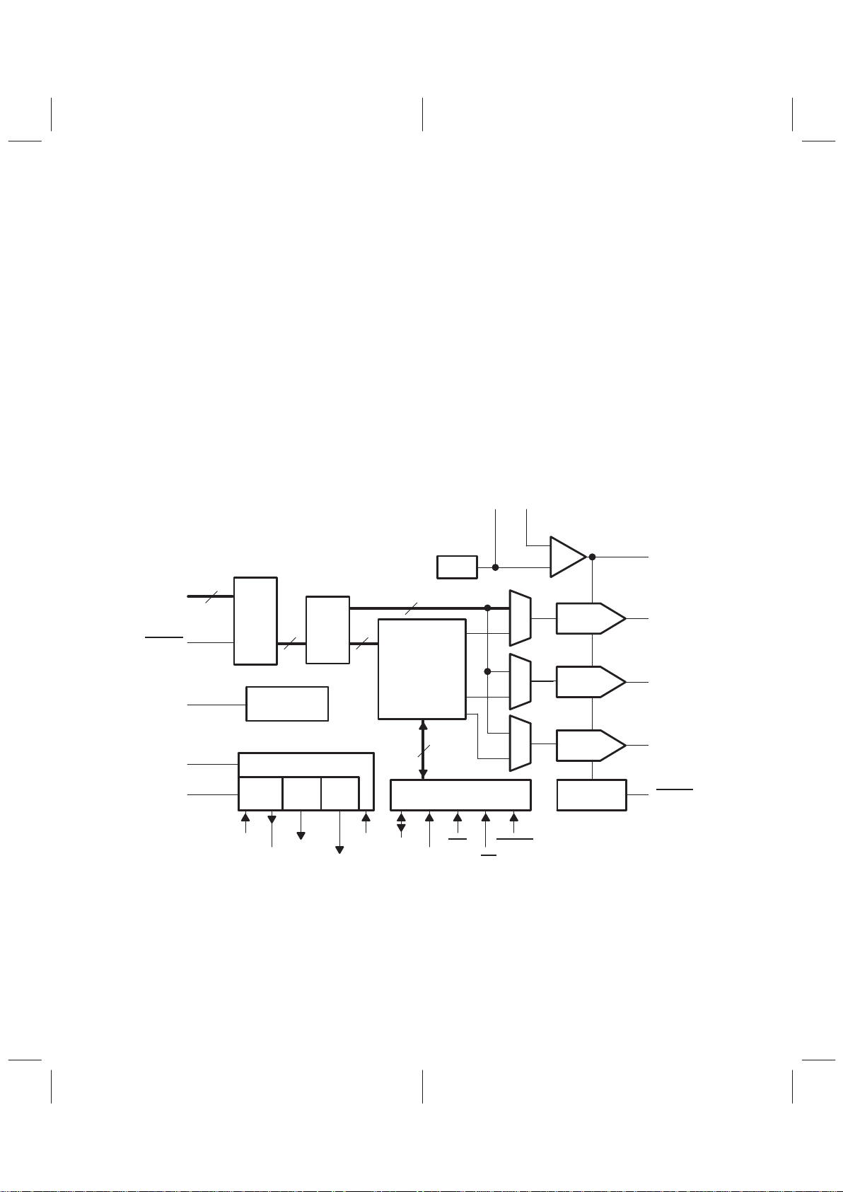
1.3 Functional Block Diagram 1–2. . . . . . . . . . . . . . . . . . . . . . . . . . . . . . . . . . . . . . . . . . . . . .
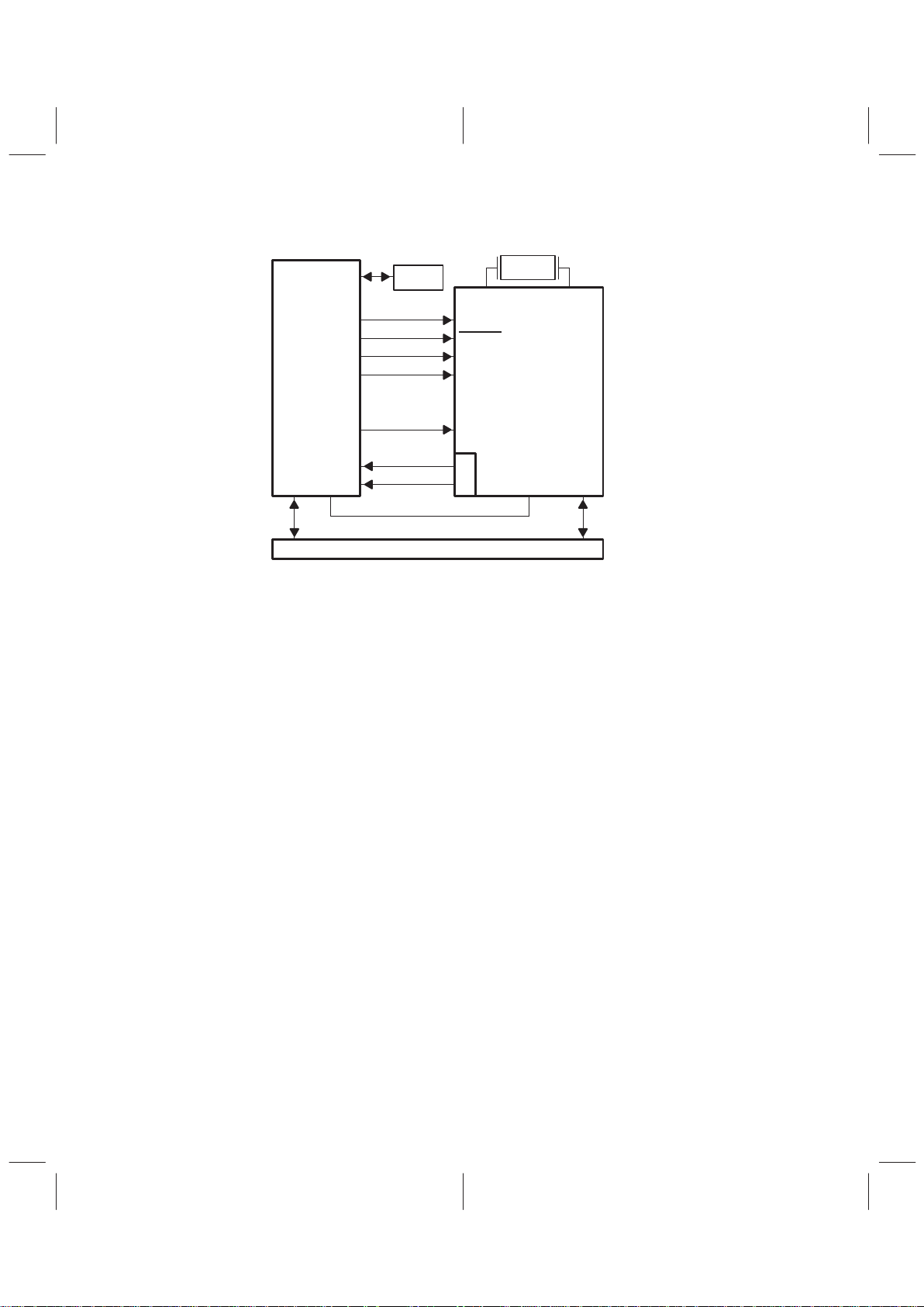
1.4 System Block Diagram 1–3. . . . . . . . . . . . . . . . . . . . . . . . . . . . . . . . . . . . . . . . . . . . . . . .
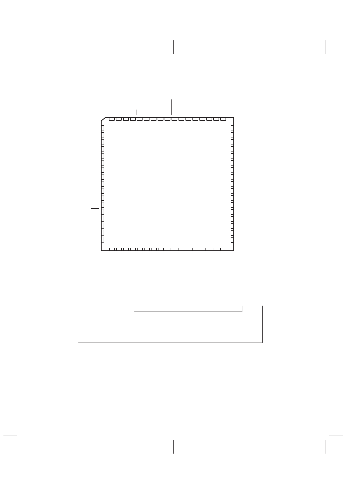
1.5 Terminal Assignments 1–4. . . . . . . . . . . . . . . . . . . . . . . . . . . . . . . . . . . . . . . . . . . . . . . . .
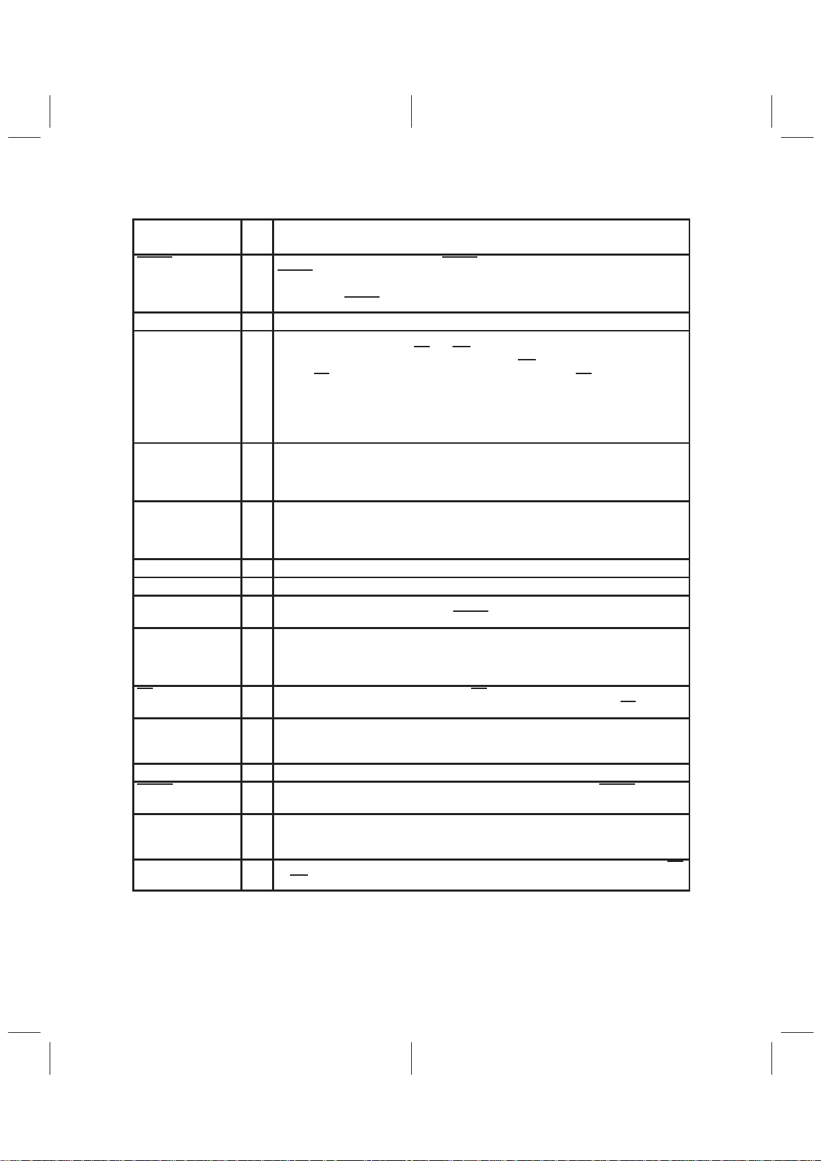
1.6 Ordering Information 1–4. . . . . . . . . . . . . . . . . . . . . . . . . . . . . . . . . . . . . . . . . . . . . . . . . .
1.7 Terminal Functions 1–5. . . . . . . . . . . . . . . . . . . . . . . . . . . . . . . . . . . . . . . . . . . . . . . . . . . .
2 Detailed Description 2–1. . . . . . . . . . . . . . . . . . . . . . . . . . . . . . . . . . . . . . . . . . . . . . . . . . . . . .
2.1 Register Descriptions 2–2. . . . . . . . . . . . . . . . . . . . . . . . . . . . . . . . . . . . . . . . . . . . . . . . . .
2.2 Internal Register Set 2–4. . . . . . . . . . . . . . . . . . . . . . . . . . . . . . . . . . . . . . . . . . . . . . . . . .
2.2.1 Write-Mode Address Register (WMA) 2–4. . . . . . . . . . . . . . . . . . . . . . . . . . . . . .
2.2.2 Read-Mode Address Register (RMA) 2–4. . . . . . . . . . . . . . . . . . . . . . . . . . . . . .
2.2.3 Look-Up Table Data Register (LUT) 2–5. . . . . . . . . . . . . . . . . . . . . . . . . . . . . . .
2.2.4 Pixel Read Mask Register (RMR) 2–5. . . . . . . . . . . . . . . . . . . . . . . . . . . . . . . . .
2.2.5 Manufacturer’s Identification Register (MIR) 2–5. . . . . . . . . . . . . . . . . . . . . . . .
2.2.6 Device Identification Register (DIR) 2–5. . . . . . . . . . . . . . . . . . . . . . . . . . . . . . .
2.2.7 Control Register 0 (CR0) 2–6. . . . . . . . . . . . . . . . . . . . . . . . . . . . . . . . . . . . . . . . .
2.2.8 Control Register 1 (CR1) 2–7. . . . . . . . . . . . . . . . . . . . . . . . . . . . . . . . . . . . . . . . .
2.2.9 Clock Synthesizer Control Register (CC) 2–8. . . . . . . . . . . . . . . . . . . . . . . . . . .
2.2.10 Clock Synthesizer Register Sets 2–9. . . . . . . . . . . . . . . . . . . . . . . . . . . . . . . . . .
2.3 Reset State 2–10. . . . . . . . . . . . . . . . . . . . . . . . . . . . . . . . . . . . . . . . . . . . . . . . . . . . . . . . . .
2.4 Programming From Reset 2–11. . . . . . . . . . . . . . . . . . . . . . . . . . . . . . . . . . . . . . . . . . . . . .
2.5 Changing Clock Frequencies 2–12. . . . . . . . . . . . . . . . . . . . . . . . . . . . . . . . . . . . . . . . . . .
2.6 Functional Descriptions 2–12. . . . . . . . . . . . . . . . . . . . . . . . . . . . . . . . . . . . . . . . . . . . . . . .
2.6.1 State Machine Access to Extended Registers 2–12. . . . . . . . . . . . . . . . . . . . . . .
2.6.2 Indexed Access to Extended Registers 2–12. . . . . . . . . . . . . . . . . . . . . . . . . . . .
2.6.3 Color Modes 2–13. . . . . . . . . . . . . . . . . . . . . . . . . . . . . . . . . . . . . . . . . . . . . . . . . . .
2.6.4 Clock Synthesizers 2–17. . . . . . . . . . . . . . . . . . . . . . . . . . . . . . . . . . . . . . . . . . . . . .
2.6.5 Clock Multiplier 2–18. . . . . . . . . . . . . . . . . . . . . . . . . . . . . . . . . . . . . . . . . . . . . . . . .
2.6.6 MPU Interface 2–19. . . . . . . . . . . . . . . . . . . . . . . . . . . . . . . . . . . . . . . . . . . . . . . . . .
2.6.7 SENSE
Output 2–20. . . . . . . . . . . . . . . . . . . . . . . . . . . . . . . . . . . . . . . . . . . . . . . . .
2.6.8 DAC Gain 2–20. . . . . . . . . . . . . . . . . . . . . . . . . . . . . . . . . . . . . . . . . . . . . . . . . . . . . .
3 Electrical Characteristics 3–1. . . . . . . . . . . . . . . . . . . . . . . . . . . . . . . . . . . . . . . . . . . . . . . . .
3.1 Absolute Maximum Ratings Over Operating Free-Air Temperature Range 3–1. . . .
3.2 Recommended Operating Conditions 3–1. . . . . . . . . . . . . . . . . . . . . . . . . . . . . . . . . . . .
3.3 Electrical Characteristics Over Recommended Full Voltage and
Temperature Ranges 3–2. . . . . . . . . . . . . . . . . . . . . . . . . . . . . . . . . . . . . . . . . . . . . . . . . .
3.3.1 DC Characteristics, Total Device 3–2. . . . . . . . . . . . . . . . . . . . . . . . . . . . . . . . . .

iv
Contents (Continued)
Section Title Page
3.3.2 AC Characteristics, Supply Current, and Pipeline Delay 3–2. . . . . . . . . . . . . .
3.4 Operating Characteristics Over Recommended Full Voltage and
Temperature Ranges 3–3. . . . . . . . . . . . . . . . . . . . . . . . . . . . . . . . . . . . . . . . . . . . . . . . . .
3.4.1 DC Characteristics, Total Device 3–3. . . . . . . . . . . . . . . . . . . . . . . . . . . . . . . . . .
3.4.2 DC Characteristics, Analog Outputs 3–3. . . . . . . . . . . . . . . . . . . . . . . . . . . . . . .
3.4.3 AC Characteristics, DAC Performance 3–4. . . . . . . . . . . . . . . . . . . . . . . . . . . . .
3.4.4 AC Characteristics, Clock Synthesizer 3–4. . . . . . . . . . . . . . . . . . . . . . . . . . . . .
3.5 Timing Requirements 3–5. . . . . . . . . . . . . . . . . . . . . . . . . . . . . . . . . . . . . . . . . . . . . . . . . .
3.5.1 Total Device 3–5. . . . . . . . . . . . . . . . . . . . . . . . . . . . . . . . . . . . . . . . . . . . . . . . . . . .
3.5.2 Pixel and Control Timing 3–5. . . . . . . . . . . . . . . . . . . . . . . . . . . . . . . . . . . . . . . . .
3.5.3 Microprocessor Port 3–5. . . . . . . . . . . . . . . . . . . . . . . . . . . . . . . . . . . . . . . . . . . . .
3.5.4 Clock Synthesizer 3–6. . . . . . . . . . . . . . . . . . . . . . . . . . . . . . . . . . . . . . . . . . . . . . .
3.6 Switching Characteristics 3–6. . . . . . . . . . . . . . . . . . . . . . . . . . . . . . . . . . . . . . . . . . . . . .
3.6.1 DAC Performance 3–6. . . . . . . . . . . . . . . . . . . . . . . . . . . . . . . . . . . . . . . . . . . . . .
3.6.2 Microprocessor Port 3–6. . . . . . . . . . . . . . . . . . . . . . . . . . . . . . . . . . . . . . . . . . . . .
3.6.3 Clock Synthesizer 3–7. . . . . . . . . . . . . . . . . . . . . . . . . . . . . . . . . . . . . . . . . . . . . . .
3.7 Timing Diagrams 3–8. . . . . . . . . . . . . . . . . . . . . . . . . . . . . . . . . . . . . . . . . . . . . . . . . . . . . .
Appendix A Application Information A–1. . . . . . . . . . . . . . . . . . . . . . . . . . . . . . . . . . . . . . . .
Appendix B Register Summary B–1. . . . . . . . . . . . . . . . . . . . . . . . . . . . . . . . . . . . . . . . . . . . .
Appendix C Mechanical Data C–1. . . . . . . . . . . . . . . . . . . . . . . . . . . . . . . . . . . . . . . . . . . . . . .

v
List of Illustrations
Figure Title Page
2–1 State Diagram for Indirect Access to Extended Registers 2–13. . . . . . . . . . . . . . . . . . . . . .
2–2 Mode 0 and Mode 3 Operation 2–16. . . . . . . . . . . . . . . . . . . . . . . . . . . . . . . . . . . . . . . . . . . . .
2–3 Mode 14, 24 Bits/Pixel, Packed in 16-Terminal Port Operation 2–17. . . . . . . . . . . . . . . . . .
2–4 Clock Synthesizer Block Diagram 2–18. . . . . . . . . . . . . . . . . . . . . . . . . . . . . . . . . . . . . . . . . . .
2–5 DAC Output Comparison Circuitry 2–21. . . . . . . . . . . . . . . . . . . . . . . . . . . . . . . . . . . . . . . . . . .
2–6 RS-343A Composite Video Output Waveforms 2–21. . . . . . . . . . . . . . . . . . . . . . . . . . . . . . . .
2–7 RS-343A Composite Video Output Waveforms (No Blank Pedestal) 2–22. . . . . . . . . . . . .
2–8 PS/2 Composite Video Output Waveforms 2–22. . . . . . . . . . . . . . . . . . . . . . . . . . . . . . . . . . .
3–1 Pixel Input and Video Output Timing 3–8. . . . . . . . . . . . . . . . . . . . . . . . . . . . . . . . . . . . . . . . .
3–2 Basic Read-Cycle Timing 3–8. . . . . . . . . . . . . . . . . . . . . . . . . . . . . . . . . . . . . . . . . . . . . . . . . .
3–3 Basic Write-Cycle Timing 3–8. . . . . . . . . . . . . . . . . . . . . . . . . . . . . . . . . . . . . . . . . . . . . . . . . .
3–4 Clock Synthesizer (OTCLKA or OTCLKB) Timing 3–9. . . . . . . . . . . . . . . . . . . . . . . . . . . . .
3–5 Clock Synthesizer Waveform Specifications (OTCLKA or OTCLKB) 3–9. . . . . . . . . . . . .

vi
List of Tables
Table Title Page
2–1 Feature Comparisons and Functional Differences of the TVP3409/ATT20C409,
ATT21C498, and ATT20C499 2–1. . . . . . . . . . . . . . . . . . . . . . . . . . . . . . . . . . . . . . . . . . . . .
2–2 Standard Register Set 2–2. . . . . . . . . . . . . . . . . . . . . . . . . . . . . . . . . . . . . . . . . . . . . . . . . . . .
2–3 State Machine Register Set 2–2. . . . . . . . . . . . . . . . . . . . . . . . . . . . . . . . . . . . . . . . . . . . . . .
2–4 Indexed Register Set 2–2. . . . . . . . . . . . . . . . . . . . . . . . . . . . . . . . . . . . . . . . . . . . . . . . . . . . .
2–5 Indexed Clock Synthesizer Configuration Registers 2–3. . . . . . . . . . . . . . . . . . . . . . . . . .
2–6 Standard Register Set 2–4. . . . . . . . . . . . . . . . . . . . . . . . . . . . . . . . . . . . . . . . . . . . . . . . . . . .
2–7 Accessing the RMR Enables Indirect Access of CR0, MIR, and DIR 2–5. . . . . . . . . . . .
2–8 Control Register 0 2–6. . . . . . . . . . . . . . . . . . . . . . . . . . . . . . . . . . . . . . . . . . . . . . . . . . . . . . . .
2–9 Control Register 1 2–7. . . . . . . . . . . . . . . . . . . . . . . . . . . . . . . . . . . . . . . . . . . . . . . . . . . . . . . .
2–10 Clock Synthesizer Control Register 2–8. . . . . . . . . . . . . . . . . . . . . . . . . . . . . . . . . . . . . . . .
2–11 Clock Synthesizer A Parameters 2–9. . . . . . . . . . . . . . . . . . . . . . . . . . . . . . . . . . . . . . . . . . .
2–12 Clock Synthesizer A Register Set Fields 2–9. . . . . . . . . . . . . . . . . . . . . . . . . . . . . . . . . . . .
2–13 Clock Synthesizer B Parameters 2–10. . . . . . . . . . . . . . . . . . . . . . . . . . . . . . . . . . . . . . . . . . .
2–14 Clock Synthesizer B Register Set Fields 2–10. . . . . . . . . . . . . . . . . . . . . . . . . . . . . . . . . . . .
2–15 I/O Transition and Logic-Level Combinations that Reset the State
Machine to State 0 2–12. . . . . . . . . . . . . . . . . . . . . . . . . . . . . . . . . . . . . . . . . . . . . . . . . . . . . . .
2–16 Access to CR0, MIR, and DIR Registers 2–13. . . . . . . . . . . . . . . . . . . . . . . . . . . . . . . . . . . .
2–17 Color Modes 2–15. . . . . . . . . . . . . . . . . . . . . . . . . . . . . . . . . . . . . . . . . . . . . . . . . . . . . . . . . . . .
2–18 Color-Mode Speeds 2–16. . . . . . . . . . . . . . . . . . . . . . . . . . . . . . . . . . . . . . . . . . . . . . . . . . . . . .
2–19 Clock Synthesizer Reset Frequencies and FS(1,0) Terminal Logic Levels 2–18. . . . . . .
2–20 Modulo 3 Counter Operation 2–19. . . . . . . . . . . . . . . . . . . . . . . . . . . . . . . . . . . . . . . . . . . . . .
2–21 Device Gain Factor (K) 2–20. . . . . . . . . . . . . . . . . . . . . . . . . . . . . . . . . . . . . . . . . . . . . . . . . . .
2–22 RS-343A Video Output Truth Table (Blank Offset Current to Equal 7.5 IRE) 2–21. . . . . .
2–23 RS-343A Video Output Truth Table (No Blank Offset Current) 2–22. . . . . . . . . . . . . . . . . .
2–24 PS/2 Video Output Truth Table (No Blank Offset Current) 2–22. . . . . . . . . . . . . . . . . . . . .

1–1
1 Introduction
The TVP3409 is intended to be a direct replacement for the ATT20C409 RAM digital-to-analog converter
(RAMDAC). The TVP3409 RAMDAC supports 8-bit multiplexed operation that can be input on 16 pixel
terminals. The TVP3409 retains register compatiblity with the ATT20C498 and ATT20C499 devices. The
TVP3409 features 24-bit packed pixel modes that provide 24-bit graphics at up to 1024 x 768 screen
resolution. Dual clock synthesizers offer two programmable and two fixed frequencies in phase-locked-loop
A (PLLA) and one programmable and three fixed frequencies in phase-locked-loop B (PLLB). After reset,
the frequencies are:
PLLA: 25.175, 28.322, 50, and 75 MHz
PLLB: 30, 40, 50, and 60 MHz
Easy identification of the RAMDAC allows the video BIOS to determine if a requested mode is available on
the hardware being used.
1.1 Features
• Functionally Interchangeable with ATT20C409
• 170/135 MHz (0.8 µm CMOS)
– 170 MHz 2:1 Multiplex 8-Bit Pseudocolor
– 73 MHz True Color
• 16-Bit Pixel Port Usable as an 8-Bit Port
– Compatible With ATT20C490 Using P(7–0)
– Compatible With ATT20C498 Using P(15–0)
• 9 Software Selectable Color Modes
– 24-Bit Packed Pixel
– 24-Bit True Color
– 8-Bit Pseudocolor
• Dual Programmable Clock Synthesizers
– Pixel Clock and Memory Clock
– Reset to 28.322-MHz and 25.175-MHz VGA Frequencies
– Strobe Input Latches Frequency Select Lines
• On-Chip PLL Clock Doubler
– 85 MHz input
– 170 MHz Pixel Output
• 2:1 and 1:1 Pixel Multiplexing
• Power Dissipation of 1.19 W at 135 MHz Typical
• 256 × 24 Color RAM
• Triple 8-Bit Monotonic Digital-to-Analog Converters (DACs)
• Software Compatible With the AT&T ATT20C498/499/409
• 68-Terminal Plastic Leaded Chip Carrier (PLCC) Package
1–2
1.2 Applications
• Performance Available With 2M-Byte Frame Buffer (noninterlaced)
– 1600 × 1280 Resolution, 8 Bits/Pixel, 60 Hz
– 1024 × 768 Resolution, 16 Bits/Pixel, 100 Hz
– 800 × 600 Resolution, 24 Bits/Pixel, Unpacked, 75 Hz
– 800 × 600 Resolution, 24 Bits/Pixel, Packed, 110 Hz
• Additional Performance Available With 3M-Byte Frame Buffer (noninterlaced)
– 1280 × 1024 Resolution, 16 Bits/Pixel, 60 Hz
– 1024 × 768 Resolution, 24 Bits/Pixel, Packed, 67 Hz
• True-Color Desktop, PC Add-in Card
• X-Windows Terminals
• Green PCs
1.3 Functional Block Diagram
M
U
X
Pixel
Latch
16
BLANK
16
Pixel
MUX
8
256 × 24/18
RAMDAC
Color RAM
M
U
X
M
U
X
Red
DAC
Green
DAC
Blue
DAC
Voltage
Compare
MPU Interface
and Registers
24
Multiplier
2×, 0.67×
Clock Synthesizers
XTAL
OSC
PLLA PLLB
P(15–0)
PCLK
FS(1,0)
STROBE
COMP
RED
GREEN
BLUEBLUE
SENSE
V
REF
24/16/8
REF RSET
XIN
XOUT
OTCLKA
OTCLKB
V
CCS
D(7–0)
RS(1,0)
WR
RD
RESET
1–3
1.4 System Block Diagram
P(15–0)
BLANK
FS(1,0)
STROBE
PLCK
A SYN
B
D(7–0)
MPU
XIN XOUT
XTAL
DRAM
Control
VCLK
MCLK
RAMDAC Control
ISA/Local/PCI Bus
RAMDAC
1–4
1.5 Terminal Assignments
28 29
GND
PCLK
P7
P6
P5
P4
P3
P2
P1
P0
V
CCS
XOUT
XIN
GND
REF
COMP
GND
60
59
58
57
56
55
54
53
52
51
50
49
48
47
46
45
44
30
10
11
12
13
14
15
16
17
18
19
20
21
22
23
24
25
26
GND
OTCLKB
P14
P15
D0
D1
D2
D3
D4
D5
D6
D7
WR
RS0
RS1
NC
GND
31 32 33 34
SENSE
P11
87 65493
BLANK
STROBERDP13
FS1
FS0
P12
GND
RED
GREEN
GND
NCNCNCNCNCNCNC
168672
35 36 37 38 39
66 65
27
NC
P10
P9
64 63 62 61
40 41 42 43
BLUE
RSET
P8NCRESET
OTCLKA
CCD
V
CCM
V
CCD
V
CCAVCCA
V
NC – No internal connection
1.6 Ordering Information
TVP3409 – XXX XX
Pixel Clock Frequency Indicator
MUST CONTAIN THREE CHARACTERS:
–135: 135-MHz pixel clock
–170: 170-MHz pixel clock
Package
MUST CONTAIN TWO LETTERS:
FN: Plastic Leaded Chip Carrier
1–5
1.7 Terminal Functions
TERMINAL
NAME NO.
I/O
DESCRIPTION
BLANK 7 I Blank (active low, TTL compatible). BLANK is latched on the rising edge of PCLK. When
BLANK
is low, the 1.44 mA current source on the analog outputs is turned off. The DACs
ignore digital input from memory . In mode 14, pixel data is aligned with the rising edge
of PCLK after BLANK
rises.
COMP 45 Compensation terminal. Bypass this terminal with an external 0.1 µF capacitor to VCC.
D(7–0) 14–21 I/O Data bus (TTL compatible). Data is transferred between the data bus and the internal
registers under control of the RD
and WR signals. In a microprocessor unit (MPU) write
operation, D(7–0) is latched on the rising edge of WR
. To read data D(7–0) from the
device, RD
must be in an active low state. The rising edge of the RD signal indicates the
end of a read cycle. Following the read cycle, the data bus goes to a high-impedance
state. Note that for 6-bit operation, color data is contained in the lower six bits of the data
bus. D0 is the LSB and D5 is the MSB. When the MPU writes color data, D6 and D7 are
ignored. During MPU read cycles, D6 and D7 are a logic 0.
FS(1,0) 2, 3 I Clock frequency select (TTL compatible). FS(1,0) select the register sets that determine
the frequency of the clock synthesizers. FS(1,0) select the register sets when CC0(7)
and CC0(3) = 0. When CC0(7) and CC0(3) = 1, bits in the CC register select the register
sets.
GND 10, 26,
36, 39,
44, 47,
60
Ground. GND terminals connect to circuit ground.
OTCLKA 8 O Output clock A (TTL compatible). Output clock from analog PLLA synthesizer.
OTCLKB 11 O Output clock B (TTL compatible). Output clock from analog PLLB synthesizer.
PCLK 59 I Pixel clock (TTL compatible). The duty cycle can be 30% to 70%. The rising edge of the
pixel clock latches the pixels and the BLANK
input.
P(12–13),
P(14–15),
P(0–7),
P(8–11)
1,4,
12,13,
51–58,
64–67
I Pixel in (TTL compatible). These terminals are latched on the rising edge of PCLK. Pixels
are presented to the DACs as color data in true-color modes and are used as addresses
in the pseudocolor mode to look up color data in the color RAM. Unused inputs should
be connected to GND.
RD 5 I Read (active low, TTL compatible). When RD is low , data is transfered from the selected
internal register to the data bus. RS(1,0) is latched on the falling edge of RD
.
RED,
GREEN,
BLUE
37,
38,
40
O Color analog out. High-impedance current sources that are capable of driving a
double-terminated 75-Ω coaxial cable.
REF 46 Voltage reference. REF should be bypassed with an external 0.1 µF capacitor to GND.
RESET 62 I Reset (TTL compatible). This input resets internal registers to 0x00. RESET programs
the clock synthesizer register sets to produce 28.322 MHz and 25.175 MHz.
RSET 42 I Reference resistor. An external resistor (R
SET
) is connected between the RSET terminal
and GND to control the magnitude of the full-scale current (refer to Section 2.6.8, DAC
Gain for more information).
RS(1,0) 23, 24 I Register select (TTL compatible). These inputs are sampled on the falling edge of RD
or WR to determine which one of the internal registers is to be accessed.
1–6
1.7 Terminal Functions (Continued)
TERMINAL
NAME NO.
I/O
DESCRIPTION
SENSE 68 O Monitor detect (active low, TTL compatible). SENSE is logic 0 when one or more of the
RED, GREEN, or BLUE outputs has exceeded the internal voltage reference level of 340
mV " 70 mV .
STROBE 6 I Strobe for reference frequency select (TTL compatible). FS(1,0) are connected to an
internal transparent latch. When STROBE is high, data can be written to FS(1,0). When
STROBE is low, the latch is closed and data cannot be written to FS(1,0). The falling edge
of STROBE latches FS(1,0). When STROBE is tied permanently high, care must be
taken to ensure that noise does not exist on the FS(1,0) inputs.
V
CCA
41, 43 Analog power. V
CCA
terminals connect to 5 V . These terminals supply the power for the
analog DACs and should be connected to a filtered supply plane.
V
CCD
9, 27 Digital power. V
CCD
terminals connect to 5 V . These terminals can be connected to the
filtered supply plane or connected to the digital supply plane of the RAMDAC.
V
CCS
50 Clock synthesizer power. V
CCS
connects to 5 V . This can be a separate supply from the
RAMDAC (see Appendix A, Application Information).
V
CCM
61 Clock multiplier power. V
CCM
connects to 5 V . This can be a separate supply from the
RAMDAC (see Appendix A, Application Information).
WR 22 I Write (active low, TTL compatible). WR controls the data transfer from the data bus to
the selected internal register. D(7–0) data is latched at the rising edge of WR
, and
RS(1,0) data is latched at the falling edge of WR
.
XIN 48 I Crystal in. XIN is the external crystal or stable frequency source connection to the internal
crystal oscillator. The recommended frequency is a 14.318 MHz system clock. When
using a crystal, it connects across XIN and XOUT.
XOUT 49 O Crystal out. XOUT is the external crystal connection to the internal crystal oscillator. All
passive components are integrated on-chip to implement a tuned resonant circuit. This
terminal should float when using a stable external frequency source connected to XIN.
2–1
2 Detailed Description
The TVP3409 RAMDAC is compatible with the architecture of the ATT20C499 and ATT20/21C498
RAMDACs. The TVP3409 contains 24-bit packed pixels on a 16-terminal interface. The device includes
dual clock synthesizers which can synthesize a pixel clock and a memory clock from a reference frequency .
The device includes a third analog PLL for pixel clock multiplication. Multiplication of 2 or 2/3 the pixel
clock is set automatically when certain color modes are programmed. Clock synthesis and clock
multiplication reduce the maximum clock speed on the board. The reduced clock speed eases high-speed
board design and FCC certification. Table 2–1 lists the feature comparisons and functional differences
between the TVP3409/ATT20C409, the ATT20C499, and the ATT21C498 RAMDACs.
The TVP3409 has been designed to allow a single board layout for assembly using either the TVP3409 or
other industry standard 44-terminal PLCC RAMDAC.
The TVP3409 includes simple indexed addressing of all control, test, and identification registers using only
two register select terminals. This supplements multiple accesses of the pixel read mask register (RMR)
used in this and other devices.
A 14.318 MHz crystal connects across the XIN and XOUT terminals when using the clock synthesizer (see
Section 1.4, System Block Diagram). Other input crystal frequencies can be used. When using a reference
frequency instead of a crystal, the signal connects to XIN and XOUT floats (disconnected).
Table 2–1. Feature Comparisons and Functional Differences of the TVP3409/ATT20C409,
ATT21C498, and ATT20C499
FEATURE TVP3409/A TT20C409 ATT20C499 ATT21C498
Pixel interface 16 terminals 24 terminals 16 terminals
Packed 24-bit pixels Yes Yes Yes
Clock synthesizers Dual Dual No
Clock multiplication factors 2, 0.67 PCLK (analog) 2, 0.67 PCLK
(analog)
2x (digital)
Multiplexer rate for 8-bit pixels 2:1 2:1 2:1
Color modes 9 13 11
Software compatible to ATT20C498 Yes Yes Yes
Control registers CR(1,0), CC0 CR(1,0), CC0 CR0
Clock synthesizer A register set A
Read/write access:
AA, AB
AC, AD
None
Read/Write
Read
Read/Write
N/A
Clock synthesizer B register set B
Read/write access:
BA, BB
BC,
BD
None
None
Read/Write
Read
Read/Write
Read/Write
N/A
MSW Terminal No Yes Yes
Package 68 PLCC 68 PLCC 44 PLCC
Manufacturer identification register (MIR) value MIR = 0x97 MIR = 0x84 MIR = 0x84
Device identification register (DIR) value DIR = 0x09 DIR = 0x99 DIR = 0x98
Revision identification No No No
Maximum speed (MHz) 170 170 170
2–2
2.1 Register Descriptions
The standard register set listed in Table 2–2 is accessed directly using RS(1,0).
Table 2–2. Standard Register Set
RS1 RS0 REGISTER ADDRESSED BY MPU REGISTER ACCESS VGA PORT
L L Write-mode address register WMA R/W 3C8
L H Look-up table data register. This register sends data to
RAMDAC color RAM.
LUT R/W 3C9
H L Pixel read mask register RMR R/W 3C6
H H Read-mode address register RMA R/W 3C7
The state machine register set is listed in T able 2–3. The RMR can also be accessed using the state machine
by setting CR0(0) = 0. When CR0(0) = 0, the registers can be accessed through the back door using the
state machine.
Table 2–3. State Machine Register Set
RS1 RS0 REGISTER ADDRESSED BY MPU REGISTER ACCESS
NUMBER
OF RMR
READS
†
CR0(0) = 0
H L Pixel read mask register RMR R/W 1–4
H L Control register 0 CR0 R/W 5
H L Manufacturer’s identification register MIR Read 6
H L Device identification register DIR Read 7
H L Reserved TST Read 8–10
†
This mode is ATT20C498 function compatible and allows access to all ATT20C498 level functionality.
The indexed register set is listed in T able 2–4. Indexed addressing must be used for programming the control
register 1 (CR1), the clock control register (CC), and the indexed clock synthesizer configuration registers
listed in Table 2–5.
Table 2–4. Indexed Register Set
RS1 RS0 REGISTER ADDRESSED BY MPU REGISTER ACCESS
INDEXED
ACCESS
CR0(0) = 1
NUMBER
OF RMR
READS
†
CR0(0) =0
H L Control register 0 CR0 R/W 0x01 5
H L Manufacturer’s identification register MIR Read 0x02 6
H L Device identification register DIR Read 0x03 7
H L Reserved TST Read 0x04 8–10
H L Control register 1 CR1 R/W 0x05 N/A
H L Clock synthesizer control register CC R/W 0x06 N/A
H L Reserved — — 0x07–0x0F —
†
This mode is ATT20C498 function compatible and allows access to all ATT20C498 level functionality.
2–3
Table 2–5. Indexed Clock Synthesizer Configuration Registers (see Notes 1, 2, and 3)
REGISTER
INDEXED
ACCESS
CR0(0) = 1
REGISTER ADDRESSED BY MPU DESCRIPTION
AA0 0x40 Reserved Reserved
AA1 0x41 Reserved Reserved
AA2 0x42 Reserved Reserved
AA3 0x43 Reserved Reserved
AB0 0x44 Reserved Reserved
AB1 0x45 Reserved Reserved
AB2 0x46 Reserved Reserved
AB3 0x47 Reserved Reserved
AC0 0x48 Clock A control register 0 of set C Feedback divider (M)
AC1 0x49 Clock A control register 1 of set C Reference (N) and postscaler (P) dividers
AC2 0x4A Clock A control register 2 of set C Reserved
AC3 0x4B Clock A control register 3 of set C Reserved
AD0 0x4C Clock A control register 0 of set D Feedback divider (M)
AD1 0x4D Clock A control register 1 of set D Reference (N) and postscaler (P) dividers
AD2 0x4E Clock A control register 2 of set D Reserved
AD3 0x4F Clock A control register 3 of set D Reserved
— 0x50–0x5F Reserved Reserved
BA0 0x60 Reserved Reserved
BA1 0x61 Reserved Reserved
BA2 0x62 Reserved Reserved
BA3 0x63 Reserved Reserved
BB0 0x64 Reserved Reserved
BB1 0x65 Reserved Reserved
BB2 0x66 Reserved Reserved
BB3 0x67 Reserved Reserved
BC0 0x68 Reserved Reserved
BC1 0x69 Reserved Reserved
BC2 0x6A Reserved Reserved
BC3 0x6B Reserved Reserved
BD0 0x6C Clock B control register 0 of set D Feedback divider (M)
BD1 0x6D Clock B control register 1 of set D Reference (N) and postscaler (P) dividers
BD2 0x6E Clock B control register 2 of set D Reserved
BD3 0x6F Clock B control register 3 of set D Reserved
— 0x70–0x7F Reserved Reserved
NOTES: 1. RS1 = 1 and RS0 = 0
2. Access = R/W
3. For RMR reads CR0(0) = 0 is not applicable.

2–4
2.2 Internal Register Set
The TVP3409 is designed to support enhanced features in a VGA-compatible architecture. A typical VGA
system only supports RS0 and RS1 register select signals. With two register select lines, access to four
registers is provided (see Table 2–2). In order to provide enhanced features, additional register locations
are required (see Table 2–4 and Table 2–5) in the VGA-accessible register space.
To provide additional registers, two more addressing schemes have been added. The first scheme uses a
back door. The back door provides access to a control register (CR0), a manufacturer’s identification
register (MIR), and a device identification register (DIR). The back door is opened by sequential reads to
the pixel read mask register (RMR). The pixel read mask register was chosen because it is not often used
in normal VGA operation.
The second method is indirect indexed addressing. Indexed addressing can be used to access the RMR,
CR0 (when CR0(0) = 1), MIR, DIR, TST , CR1, CC and the registers in Table 2–5. Indexed addressing is the
only way to read or write CR1, CC, and the registers in Table 2–5.
T o use this method, set CR0(0) = 1 using the back door (multiple accesses to the RMR). W rite the address
register (WMA) with the address of the register to be read or written. The index of the registers accessible
indirectly are listed in the indexed access column in T ables 2–4 and 2–5. Perform a read or write operation
when RS(1,0) = 10. The value is read from or written to the register indexed by the contents of the address
register.
2.2.1 Write-Mode Address Register (WMA)
This register holds an 8-bit value that is used as an index when writing to the look-up table (LUT) data register
or extended indexed registers. For the LUT data register, this register points to one of the 256 RAMDAC
color RAM locations. Each of the RAMDAC color RAM locations are 24-bits wide (8-bits read, 8-bits green
and 8-bit blue). To write all 24-bits of a RAMDAC color RAM location, three successive writes are made to
the same address. After the sequence of three writes is completed, the 24-bit value is transferred to the
RAMDAC color RAM.
The LUT and RMR registers listed in Table 2–6 apply only in the 8-bit modes.
Table 2–6. Standard Register Set
REGISTER
REGISTER
TYPE
7 6 5 4 3 2 1 0
WMA
Read
Write
A7 A6 A5 A4 A3 A2 A1 A0
LUT
Read
Write
D7 D6 D5 D4 D3 D2 D1 D0
RMR
Read
Write
M7 M6 M5 M4 M3 M2 M1 M0
RMA
Read
Write
A7 A6 A5 A4 A3 A2 A1 A0
This register is only used while writing to the LUT data register or reading or writing the extended indexed
registers. After this register is set to the desired index, MPU data can be written to the LUT data register or
register values can be written to extended indexed registers. The WMA register is autoincrementing when
writing to the LUT. When three writes to the LUT data register are complete, the LUT data register data is
written to the RAMDAC color RAM and the WMA register increments by one. For this reason, the WMA
should be written every time extended indexed registers are accessed.
2.2.2 Read-Mode Address Register (RMA)
This register holds an 8-bit value that is used as an index when reading from the LUT data register or reading
or writing the extended indexed registers. To read all 24-bits of a RAMDAC color RAM location, three
successive reads are made to the same address.

2–5
This register is autoincrementing when reading the LUT . When written, the RMA reads the RAMDAC color
RAM data into the LUT data register then the RMA increments by one. When the three reads from the LUT
data register are complete, the device transfers new RAMDAC color RAM data at the RMA address into the
LUT data register and the RMA increments by one again. When using the RMA for access to the indexed
registers, write a value one less than the desired index. The RMA register increments by one before using
the index to access the information being read or written.
2.2.3 Look-Up Table Data Register (LUT)
This register is the data port through which reads and writes are made to the RAMDAC color RAM. The
write-mode address register or read-mode address register specifies which RAMDAC color RAM location
is to be accessed. This register is an 8-bit port to a 24-bit location. Three accesses are needed to read or
write the LUT data register. Because both the write-mode address and read-mode address registers are
autoincrementing, accesses to this port should be made three at a time to avoid leaving a partially read or
written LUT data register. A partially written data register is not transferred to the RAMDAC color RAM. The
blue value must be written before the RAMDAC color RAM is updated.
2.2.4 Pixel Read Mask Register (RMR)
The contents of the RMR can be accessed by the MPU at any time and are not initialized on power up. The
RMR bits are logically ANDed with the 8-bit pixels in pseudocolor mode. In true-color modes, pixels are not
modified by the RMR. A logic one stored in a data bit of the RMR leaves the corresponding bit in the pixel
unchanged. A logic 0 in the RMR sets the pixel bit to 0. Bit D0 of the RMR corresponds to pixel bit P0.
Reading the RMR four times without accessing another RAMDAC register directs the next (fifth) read or
write access to control register 0. The sixth consecutive read from the RMR returns the MIR. The seventh
consecutive read from the RMR returns the DIR (see Table 2–7).
Table 2–7. Accessing the RMR Enables Indirect Access of CR0, MIR, and DIR
RMR
READ
NO.
REGISTER
NAME
REGISTER
TYPE
7 6 5 4 3 2 1 0
5 CR0
Read
Write
CR7 CR6 CR5 CR4 CR3 CR2 CR1 CR0
6 MIR
Read
Only
1 0 0 0 0 1 0 0
7 DIR
Read
Only
0 0 0 0 1 0 0 1
The eighth, ninth, and tenth consecutive reads from the RMR return don’t care values. These states are
defined in the back-door state machine to maintain compatibility with the ATT20C409, ATT20C499, and
ATT20C498 test registers. These test registers are not being implemented in the TVP3409 and, therefore,
do not return usable information (see Figure 2–1).
2.2.5 Manufacturer’s Identification Register (MIR)
This 8-bit register contains an 8-bit value to identify the manufacturer of the RAMDAC. The MIR is read by
reading the RMR six times without accessing any other RAMDAC register. The first four reads return the
contents of the RMR. The fifth read returns the CR0 contents. The sixth read returns the MIR contents (97
hex). The seventh read returns the DIR contents.
2.2.6 Device Identification Register (DIR)
This 8-bit register contains an 8-bit value to identify the type of RAMDAC. The DIR is read by reading the
RMR seven times without accessing any other RAMDAC register. The TVP3409 returns the value 09 hex.

2–6
2.2.7 Control Register 0 (CR0)
Control register 0 is written to or read by the MPU. CR0 is not initialized at power on. CR0 bit 0 is the least
significant bit (LSB) in the control register and corresponds to D0 of the MPU port. Table 2–8 defines the
bits of the control register.
CR0 bits (7–4) determine the color mode as shown in Table 2–17.
Setting CR0(3) to a 1 places the RAMDAC in power-down mode. In the power-down state, the device retains
the information in the color look-up table. Access to the color look-up table is disabled during the
power-down mode. The internal registers can be written to while the device is in the power-down mode. The
crystal oscillator and clock synthesizers are powered down separately.
The CR0(2) bit is reserved.
The 8/6 select bit CR0(1) determines whether the MPU port reads and writes 8 bits or 6 bits of color data
to the color look up table RAM. In 6-bit mode, color data is on the lower 6 bits of the data bus, with D0 being
the LSB and D5 the most significant bit (MSB) of color data. When writing color data, D6 and D7 are ignored.
During color read cycles, D6 and D7 are logic 0. Note that in the 6-bit mode, the full scale output current is
about 1.5% lower than when in the 8-bit mode. This is a result of the two LSBs of each 8-bit DAC always
being a logic 0 in the 6-bit mode. In the 8-bit color mode, bit D0 is the color data LSB and bit D7 is the MSB.
The CR0(0) bit controls access to the extended registers.
This register is operational upon power up. It can be read or written to by the MPU at any time and it is not
initialized. All bits are set to 0 upon asserting RESET
. T o read from or write to this register, use the internal
state machine for access by reading the RMR (see Table 2–3).
Table 2–8. Control Register 0
BIT NAME DESCRIPTION
CR0(7–4) Color Mode These bits control the color modes (see Tables 2–17).
CR0(3) Power Down
(RAMDAC)
Logic 0: Normal operation
Logic 1: Sleep
CR0(3) powers the RAMDAC off. The device does not power up for MPU updates.
The data in the LUT is maintained during power down. Internal registers can be
accessed while the RAMDAC is powered down. CR1(3,2) powers down the clock
synthesizers (for green PC compatibility).
CR0(2) Reserved
CR0(1) 8/6 Select Logic 0: 6-bit data to the DAC
Logic 1: 8-bit data to the DAC
A logic 0 specifies 6 bits per DAC operation (256K possible colors). A logic 1
specifies 8 bits per DAC operation (16M possible colors).
CR0(0) Extended Register
Enable (Indirect or
Indexed Access)
Logic 0: Index accesses disabled to extended registers.
Logic 1: Index accesses enabled to extended registers.
Bit 0 controls access to the extended registers. When bit 0 is a logic 0, access to the
extended registers is enabled by multiple accesses to the RMR (state machine
addressing). This does not allow access to CR1, CC, or the clock configuration
registers. When this bit is a logic 1, all extended registers can be accessed with
indexed addressing using the WMA or RMA register as an address pointer and
RS(1,0)= 10 for the data register.
 Loading...