

Texas Instruments TVP3026-250CPCE, TVP3026-250MDN, TVP3026-230CPCE, TVP3026-220PCE, TVP3026-135PCE Datasheet
...
TVP3026
Data Manual
V ideo Interface Palette
SLAS098B
July 1996
Printed on Recycled Paper

ii
IMPORTANT NOTICE
Texas Instruments (TI) reserves the right to make changes to its products or to
discontinue any semiconductor product or service without notice, and advises its
customers to obtain the latest version of relevant information to verify, before placing
orders, that the information being relied on is current.
TI warrants performance of its semiconductor products and related software to the
specifications applicable at the time of sale in accordance with TI’s standard warranty.
T esting and other quality control techniques are utilized to the extent TI deems necessary
to support this warranty. Specific testing of all parameters of each device is not
necessarily performed, except those mandated by government requirements.
Certain applications using semiconductor products may involve potential risks of death,
personal injury, or severe property or environmental damage (“Critical Applications”).
TI SEMICONDUCTOR PRODUCTS ARE NOT DESIGNED, INTENDED,
AUTHORIZED, OR WARRANTED TO BE SUITABLE FOR USE IN LIFE-SUPPORT
APPLICATIONS, DEVICES OR SYSTEMS OR OTHER CRITICAL APPLICATIONS.
Inclusion of TI products in such applications is understood to be fully at the risk of the
customer. Use of TI products in such applications requires the written approval of an
appropriate TI officer . Questions concerning potential risk applications should be directed
to TI through a local SC sales office.
In order to minimize risks associated with the customer’s applications, adequate design
and operating safeguards should be provided by the customer to minimize inherent or
procedural hazards.
TI assumes no liability for applications assistance, customer product design, software
performance, or infringement of patents or services described herein. Nor does TI
warrant or represent that any license, either express or implied, is granted under any
patent right, copyright, mask work right, or other intellectual property right of TI covering
or relating to any combination, machine, or process in which such semiconductor
products or services might be or are used.
Copyright 1996, Texas Instruments Incorporated

iii
Contents
Section Title Page
1 Introduction 1–1. . . . . . . . . . . . . . . . . . . . . . . . . . . . . . . . . . . . . . . . . . . . . . . . . . . . . . . . . . . . . . .
1.1 Features 1–2. . . . . . . . . . . . . . . . . . . . . . . . . . . . . . . . . . . . . . . . . . . . . . . . . . . . . . . . . . . . . .
1.2 Functional Block Diagram 1–3. . . . . . . . . . . . . . . . . . . . . . . . . . . . . . . . . . . . . . . . . . . . . . .
1.3 Terminal Assignments 1–4. . . . . . . . . . . . . . . . . . . . . . . . . . . . . . . . . . . . . . . . . . . . . . . . . .
1.4 Ordering Information 1–5. . . . . . . . . . . . . . . . . . . . . . . . . . . . . . . . . . . . . . . . . . . . . . . . . . .
1.5 Terminal Functions 1–5. . . . . . . . . . . . . . . . . . . . . . . . . . . . . . . . . . . . . . . . . . . . . . . . . . . . .
2 Detailed Description 2–1. . . . . . . . . . . . . . . . . . . . . . . . . . . . . . . . . . . . . . . . . . . . . . . . . . . . . . .
2.1 Microprocessor Unit Interface 2–1. . . . . . . . . . . . . . . . . . . . . . . . . . . . . . . . . . . . . . . . . . .
2.1.1 8/6
Operation 2–3. . . . . . . . . . . . . . . . . . . . . . . . . . . . . . . . . . . . . . . . . . . . . . . . .
2.1.2 Pixel Read-Mask Register 2–3. . . . . . . . . . . . . . . . . . . . . . . . . . . . . . . . . . . . . .
2.1.3 Palette-Page Register 2–3. . . . . . . . . . . . . . . . . . . . . . . . . . . . . . . . . . . . . . . . . .
2.1.4 Cursor and Overscan Color Registers 2–4. . . . . . . . . . . . . . . . . . . . . . . . . . . .
2.2 Color-Palette RAM 2–4. . . . . . . . . . . . . . . . . . . . . . . . . . . . . . . . . . . . . . . . . . . . . . . . . . . . .
2.2.1 Writing to Color-Palette RAM 2–5. . . . . . . . . . . . . . . . . . . . . . . . . . . . . . . . . . . .
2.2.2 Reading From Color-Palette RAM 2–5. . . . . . . . . . . . . . . . . . . . . . . . . . . . . . .
2.3 Clock Selection 2–5. . . . . . . . . . . . . . . . . . . . . . . . . . . . . . . . . . . . . . . . . . . . . . . . . . . . . . . .
2.4 PLL Clock Generators 2–6. . . . . . . . . . . . . . . . . . . . . . . . . . . . . . . . . . . . . . . . . . . . . . . . . .
2.4.1 Pixel Clock PLL 2–8. . . . . . . . . . . . . . . . . . . . . . . . . . . . . . . . . . . . . . . . . . . . . . .
2.4.2 Memory Clock PLL 2–10. . . . . . . . . . . . . . . . . . . . . . . . . . . . . . . . . . . . . . . . . . .
2.4.3 Loop Clock PLL 2–12. . . . . . . . . . . . . . . . . . . . . . . . . . . . . . . . . . . . . . . . . . . . . .
2.5 Frame-Buffer Interface 2–16. . . . . . . . . . . . . . . . . . . . . . . . . . . . . . . . . . . . . . . . . . . . . . . .
2.5.1 Frame-Buffer Interface 2–17. . . . . . . . . . . . . . . . . . . . . . . . . . . . . . . . . . . . . . . .
2.5.2 Frame-Buffer Timing Without Using SCLK 2–17. . . . . . . . . . . . . . . . . . . . . . .
2.5.3 Frame-Buffer Timing Using SCLK 2–17. . . . . . . . . . . . . . . . . . . . . . . . . . . . . . .
2.5.4 Split Shift-Register-Transfer Support 2–18. . . . . . . . . . . . . . . . . . . . . . . . . . . .
2.6 Multiplexing Modes of Operation 2–19. . . . . . . . . . . . . . . . . . . . . . . . . . . . . . . . . . . . . . . .
2.6.1 Little-Endian and Big-Endian Data Format 2–19. . . . . . . . . . . . . . . . . . . . . . .
2.6.2 VGA Modes 2–19. . . . . . . . . . . . . . . . . . . . . . . . . . . . . . . . . . . . . . . . . . . . . . . . .
2.6.3 Pseudo-Color Mode 2–19. . . . . . . . . . . . . . . . . . . . . . . . . . . . . . . . . . . . . . . . . .
2.6.4 Direct-Color Mode 2–20. . . . . . . . . . . . . . . . . . . . . . . . . . . . . . . . . . . . . . . . . . . .
2.6.5 True-Color Mode 2–20. . . . . . . . . . . . . . . . . . . . . . . . . . . . . . . . . . . . . . . . . . . . .
2.6.6 Packed-24 Mode 2–21. . . . . . . . . . . . . . . . . . . . . . . . . . . . . . . . . . . . . . . . . . . . .
2.6.7 Multiplex-Control Registers 2–23. . . . . . . . . . . . . . . . . . . . . . . . . . . . . . . . . . . .
2.7 On-Chip Cursor 2–31. . . . . . . . . . . . . . . . . . . . . . . . . . . . . . . . . . . . . . . . . . . . . . . . . . . . . . .
2.7.1 Cursor RAM 2–31. . . . . . . . . . . . . . . . . . . . . . . . . . . . . . . . . . . . . . . . . . . . . . . . .
2.7.2 Cursor Positioning 2–32. . . . . . . . . . . . . . . . . . . . . . . . . . . . . . . . . . . . . . . . . . . .
2.7.3 Three-Color 64 x 64 Cursor 2–33. . . . . . . . . . . . . . . . . . . . . . . . . . . . . . . . . . . .
2.7.4 Interlaced Cursor Operation 2–34. . . . . . . . . . . . . . . . . . . . . . . . . . . . . . . . . . .

iv
Contents (Continued)
Section Title Page
2.8 Port-Select and Color-Key Switching 2–34. . . . . . . . . . . . . . . . . . . . . . . . . . . . . . . . . . . .
2.8.1 Port-Select Switching 2–35. . . . . . . . . . . . . . . . . . . . . . . . . . . . . . . . . . . . . . . . .
2.8.2 Color-Key Switching 2–35. . . . . . . . . . . . . . . . . . . . . . . . . . . . . . . . . . . . . . . . . .
2.9 Overscan Border 2–36. . . . . . . . . . . . . . . . . . . . . . . . . . . . . . . . . . . . . . . . . . . . . . . . . . . . .
2.10 Horizontal Zooming 2–37. . . . . . . . . . . . . . . . . . . . . . . . . . . . . . . . . . . . . . . . . . . . . . . . . . .
2.11 Test Functions 2–37. . . . . . . . . . . . . . . . . . . . . . . . . . . . . . . . . . . . . . . . . . . . . . . . . . . . . . . .
2.11.1 16-Bit CRC 2–37. . . . . . . . . . . . . . . . . . . . . . . . . . . . . . . . . . . . . . . . . . . . . . . . . .
2.11.2 Sense Comparator Output and Test Register 2–38. . . . . . . . . . . . . . . . . . . . .
2.11.3 Identification Code 2–38. . . . . . . . . . . . . . . . . . . . . . . . . . . . . . . . . . . . . . . . . . . .
2.1 1.4 Silicon Revision 2–39. . . . . . . . . . . . . . . . . . . . . . . . . . . . . . . . . . . . . . . . . . . . . .
2.12 General-Purpose I/O Register and Terminals 2–39. . . . . . . . . . . . . . . . . . . . . . . . . . . . .
2.13 Reset 2–39. . . . . . . . . . . . . . . . . . . . . . . . . . . . . . . . . . . . . . . . . . . . . . . . . . . . . . . . . . . . . . .
2.14 Analog Output Specifications 2–39. . . . . . . . . . . . . . . . . . . . . . . . . . . . . . . . . . . . . . . . . . .
2.15 Register Definitions 2–42. . . . . . . . . . . . . . . . . . . . . . . . . . . . . . . . . . . . . . . . . . . . . . . . . . .
2.15.1 General-Control Register 2–42. . . . . . . . . . . . . . . . . . . . . . . . . . . . . . . . . . . . . .
2.15.2 Miscellaneous-Control Register 2–42. . . . . . . . . . . . . . . . . . . . . . . . . . . . . . . .
2.15.3 Indirect Cursor-Control Register 2–43. . . . . . . . . . . . . . . . . . . . . . . . . . . . . . . .
2.15.4 Direct Cursor-Control Register 2–43. . . . . . . . . . . . . . . . . . . . . . . . . . . . . . . . .
2.15.5 Cursor-Position (x, y) Registers 2–44. . . . . . . . . . . . . . . . . . . . . . . . . . . . . . . .
2.15.6 Color-Key Control Register 2–45. . . . . . . . . . . . . . . . . . . . . . . . . . . . . . . . . . . .
2.15.7 Color-Key (Overlay, Red, Green, Blue) Registers 2–46. . . . . . . . . . . . . . . . .
2.15.8 CRC Remainder LSB and MSB Registers 2–46. . . . . . . . . . . . . . . . . . . . . . .
2.15.9 CRC Bit Select Register 2–46. . . . . . . . . . . . . . . . . . . . . . . . . . . . . . . . . . . . . . .
3 Electrical Characteristics 3–1. . . . . . . . . . . . . . . . . . . . . . . . . . . . . . . . . . . . . . . . . . . . . . . . . .
3.1 Absolute Maximum Ratings Over Operating Free-Air Temperature Range 3–1. . . .
3.2 Recommended Operating Conditions 3–1. . . . . . . . . . . . . . . . . . . . . . . . . . . . . . . . . . . . .
3.3 Electrical Characteristics 3–2. . . . . . . . . . . . . . . . . . . . . . . . . . . . . . . . . . . . . . . . . . . . . . . .
3.4 Operating Characteristics 3–3. . . . . . . . . . . . . . . . . . . . . . . . . . . . . . . . . . . . . . . . . . . . . . .
3.5 Timing Requirements 3–4. . . . . . . . . . . . . . . . . . . . . . . . . . . . . . . . . . . . . . . . . . . . . . . . . . .
3.6 Switching Characteristics 3–5. . . . . . . . . . . . . . . . . . . . . . . . . . . . . . . . . . . . . . . . . . . . . . .
3.7 Timing Diagrams 3–7. . . . . . . . . . . . . . . . . . . . . . . . . . . . . . . . . . . . . . . . . . . . . . . . . . . . . . .
Appendix A Frequency Synthesis PLL Register Settings A–1. . . . . . . . . . . . . . . . . . . . . .
Appendix B PLL Programming Examples B–1. . . . . . . . . . . . . . . . . . . . . . . . . . . . . . . . . . . .
Appendix C Recommended Clock Programming Procedures C–1. . . . . . . . . . . . . . . . . .
Appendix D PC-Board Layout Considerations D–1. . . . . . . . . . . . . . . . . . . . . . . . . . . . . . . .
Appendix E Crystal Selection E–1. . . . . . . . . . . . . . . . . . . . . . . . . . . . . . . . . . . . . . . . . . . . . . .
Appendix F Changes Made For TVP3026 Revision B F–1. . . . . . . . . . . . . . . . . . . . . . . . . .
Appendix G Mechanical Data G–1. . . . . . . . . . . . . . . . . . . . . . . . . . . . . . . . . . . . . . . . . . . . . . . .

v
List of Illustrations
Figure Title Page
1–1. Functional Block Diagram 1–3. . . . . . . . . . . . . . . . . . . . . . . . . . . . . . . . . . . . . . . . . . . . . . . .
1–2. Terminal Assignments 1–4. . . . . . . . . . . . . . . . . . . . . . . . . . . . . . . . . . . . . . . . . . . . . . . . . . .
2–1. TVP3026 Clocking Scheme 2–8. . . . . . . . . . . . . . . . . . . . . . . . . . . . . . . . . . . . . . . . . . . . . .
2–2. Loop Clock PLL Operation 2–12. . . . . . . . . . . . . . . . . . . . . . . . . . . . . . . . . . . . . . . . . . . . . .
2–3. Typical Configuration – VRAM Clocked by Accelerator 2–16. . . . . . . . . . . . . . . . . . . . . .
2–4. Typical Configuration – VRAM Clocked by TVP3026 2–16. . . . . . . . . . . . . . . . . . . . . . . .
2–5. Frame-Buffer Timing Without Using SCLK 2–17. . . . . . . . . . . . . . . . . . . . . . . . . . . . . . . . .
2–6. Frame-Buffer Timing Using SCLK 2–18. . . . . . . . . . . . . . . . . . . . . . . . . . . . . . . . . . . . . . . .
2–7. Frame-Buffer Timing Using SCLK (With First SCLK Pulse Relocated) 2–18. . . . . . . . .
2–8. Cursor-RAM Organization 2–32. . . . . . . . . . . . . . . . . . . . . . . . . . . . . . . . . . . . . . . . . . . . . . .
2–9. Cursor Positioning 2–33. . . . . . . . . . . . . . . . . . . . . . . . . . . . . . . . . . . . . . . . . . . . . . . . . . . . .
2–10. Overscan 2–37. . . . . . . . . . . . . . . . . . . . . . . . . . . . . . . . . . . . . . . . . . . . . . . . . . . . . . . . . . . . .
2–11. CRC Algorithm 2–38. . . . . . . . . . . . . . . . . . . . . . . . . . . . . . . . . . . . . . . . . . . . . . . . . . . . . . . .
2–12. Equivalent Circuit of the Current Output (IOG) 2–40. . . . . . . . . . . . . . . . . . . . . . . . . . . . .
2–13. Composite Video Output (With 0 IRE, 8-Bit Output) 2–41. . . . . . . . . . . . . . . . . . . . . . . . .
2–14. Composite Video Output (With 7.5 IRE, 8-Bit Output) 2–41. . . . . . . . . . . . . . . . . . . . . . .
3–1. MPU Interface Timing 3–11. . . . . . . . . . . . . . . . . . . . . . . . . . . . . . . . . . . . . . . . . . . . . . . . . . .
3–2. Video Input/Output Timing 3–12. . . . . . . . . . . . . . . . . . . . . . . . . . . . . . . . . . . . . . . . . . . . . .

vi
List of Tables
Table Title Page
2–1. Direct Register Map 2–1. . . . . . . . . . . . . . . . . . . . . . . . . . . . . . . . . . . . . . . . . . . . . . . . . . . . .
2–2. Indirect Register Map (Extended Registers) 2–2. . . . . . . . . . . . . . . . . . . . . . . . . . . . . . . .
2–3. Allocation of Palette-Page Register Bits 2–3. . . . . . . . . . . . . . . . . . . . . . . . . . . . . . . . . . . .
2–4. Color Register Address Format 2–4. . . . . . . . . . . . . . . . . . . . . . . . . . . . . . . . . . . . . . . . . . .
2–5. Clock-Selection Register Bits CSR (6 – 4) 2–6. . . . . . . . . . . . . . . . . . . . . . . . . . . . . . . . . .
2–6. Clock-Selection Register Bits CSR (3 – 0) 2–6. . . . . . . . . . . . . . . . . . . . . . . . . . . . . . . . . .
2–7. PLL Top Level Registers 2–7. . . . . . . . . . . . . . . . . . . . . . . . . . . . . . . . . . . . . . . . . . . . . . . . .
2–8. PLL Address Register 2–7. . . . . . . . . . . . . . . . . . . . . . . . . . . . . . . . . . . . . . . . . . . . . . . . . . .
2–9. PLL Data Register Pointer Format 2–7. . . . . . . . . . . . . . . . . . . . . . . . . . . . . . . . . . . . . . . . .
2–10. Pixel Clock PLL Registers 2–9. . . . . . . . . . . . . . . . . . . . . . . . . . . . . . . . . . . . . . . . . . . . . . . .
2–11. Pixel Clock PLL Frequency Selection 2–9. . . . . . . . . . . . . . . . . . . . . . . . . . . . . . . . . . . . . .
2–12. MCLK PLL Registers 2–10. . . . . . . . . . . . . . . . . . . . . . . . . . . . . . . . . . . . . . . . . . . . . . . . . . .
2–13. MCLK/Loop Clock Control Register 2–11. . . . . . . . . . . . . . . . . . . . . . . . . . . . . . . . . . . . . . .
2–14. Loop Clock PLL Registers 2–13. . . . . . . . . . . . . . . . . . . . . . . . . . . . . . . . . . . . . . . . . . . . . . .
2–15. Loop Clock PLL Settings for Packed-24 Mode 2–14. . . . . . . . . . . . . . . . . . . . . . . . . . . . .
2–16. Latch-Control Register 2–15. . . . . . . . . . . . . . . . . . . . . . . . . . . . . . . . . . . . . . . . . . . . . . . . . .
2–17. Multiplex Mode and Bus-Width Selection 2–24. . . . . . . . . . . . . . . . . . . . . . . . . . . . . . . . . .
2–18. Pseudo-Color Mode Pixel-Latching Sequence 2–27. . . . . . . . . . . . . . . . . . . . . . . . . . . . .
2–19. Packed-24 Formats 2–28. . . . . . . . . . . . . . . . . . . . . . . . . . . . . . . . . . . . . . . . . . . . . . . . . . . .
2–20. Direct-Color Mode Pixel-Latching Sequence (Little-Endian) 2–29. . . . . . . . . . . . . . . . . .
2–21. Direct-Color Mode Pixel-Latching Sequence (Big-Endian) 2–30. . . . . . . . . . . . . . . . . . .
2–22. Cursor RAM Vs. Color Selection 2–33. . . . . . . . . . . . . . . . . . . . . . . . . . . . . . . . . . . . . . . . .
2–23. Port-Select Switching 2–35. . . . . . . . . . . . . . . . . . . . . . . . . . . . . . . . . . . . . . . . . . . . . . . . . . .
2–24. Sense-Test Register Results 2–38. . . . . . . . . . . . . . . . . . . . . . . . . . . . . . . . . . . . . . . . . . . . .
2–25. General Purpose I/O Registers 2–39. . . . . . . . . . . . . . . . . . . . . . . . . . . . . . . . . . . . . . . . . .
2–26. General-Control Register 2–42. . . . . . . . . . . . . . . . . . . . . . . . . . . . . . . . . . . . . . . . . . . . . . . .
2–27. Miscellaneous-Control Register 2–42. . . . . . . . . . . . . . . . . . . . . . . . . . . . . . . . . . . . . . . . . .
2–28. Indirect Cursor-Control Register 2–43. . . . . . . . . . . . . . . . . . . . . . . . . . . . . . . . . . . . . . . . . .
2–29. Direct Cursor-Control Register 2–43. . . . . . . . . . . . . . . . . . . . . . . . . . . . . . . . . . . . . . . . . . .
2–30. Cursor Position (x, y) Registers 2–44. . . . . . . . . . . . . . . . . . . . . . . . . . . . . . . . . . . . . . . . . .
2–31. Color-Key Control Register 2–45. . . . . . . . . . . . . . . . . . . . . . . . . . . . . . . . . . . . . . . . . . . . . .
2–32. Color-Key Low and High Registers 2–46. . . . . . . . . . . . . . . . . . . . . . . . . . . . . . . . . . . . . . .
2–33. CRC Remainder LSB and MSB Registers 2–46. . . . . . . . . . . . . . . . . . . . . . . . . . . . . . . . .
2–34. CRC Bit Select Register 2–46. . . . . . . . . . . . . . . . . . . . . . . . . . . . . . . . . . . . . . . . . . . . . . . .

1–1
1 Introduction
The TVP3026 is an advanced video interface palette (VIP) from T exas Instruments implemented in EPIC
0.2-micron CMOS process. The TVP3026 is a 64-bit VIP that supports packed-24 modes enabling 24-bit
true color and high resolution at the same time without excessive amounts of frame buffer memory. For
example, a 24-bit true color display with 1280 x 1024 resolution may be packed into 4M of VRAM. A
PLL-generated, 50 % duty cycle reference clock is output in the packed-24 modes, maximizing VRAM cycle
time and the screen refresh rate.
The TVP3026 supports all of the pixel formats of the TVP3020 VIP. Data can be split into 4 or 8 bit planes
for pseudo-color mode or split into 12-, 16- or 24-bit true-color and direct-color modes. For the 24-bit direct
color modes, an 8-bit overlay plane is available. The 16-bit direct- and true-color modes can be configured
to IBM XGA
(5, 6, 5), TARGA (1, 5, 5, 5), or 16-bit/pixel (6, 6, 4) configuration as another existing format.
An additional 12-bit mode with 4-bit overlay (4, 4, 4, 4) is supported with 4 bits for each color and overlay.
All color modes support selection of little or big endian data format for the pixel bus. Additionally, the device
is also software compatible with the INMOS IMSG176/8 and Brooktree Bt476/8 color palettes.
Two fully programmable phase-locked loops (PLLs) for pixel clock and memory clock functions are
provided, as well as a simple frequency doubler for dramatic improvements in graphics system cost and
integration. A third loop clock PLL is incorporated making pixel data latch timing much simpler than with other
existing color palettes. In addition, four digital clock inputs (2 TTL- and 2 ECL /TTL-compatible) may be
utilized and are software selectable. The video clock provides a software selected divide ratio of the chosen
pixel clock. The shift clock output may be used directly as the VRAM shift clock. The reference clock output
is driven by the loop clock PLL and provides a timing reference to the graphics accelerator.
Like the TVP3020, the TVP3026 also integrates a complete IBM XGA-compatible hardware cursor on chip,
making significant graphics performance enhancements possible. Additionally, hardware port select and
color-keyed switching functions are provided, giving the user several efficient means of producing graphical
overlays on direct-color backgrounds.
The TVP3026 has three 256-by-8 color lookup tables with triple 8-bit video digital-to-analog converters
(DACs) capable of directly driving a doubly terminated 75-Ω line. The lookup tables are designed with a
dual-ported RAM architecture that enables ultra-high speed operation. Sync generation is incorporated on
the green output channel. Horizontal sync (HSYNC) and vertical sync (VSYNC) are pipeline delayed
through the device and optionally inverted to indicate screen resolution to the monitor. A palette-page
register is available to select from multiple color maps in RAM when 4 bit planes are used. This allows the
screen colors to be changed with only one microprocessor write cycle.
The device features a separate VGA bus which supports the integrated VGA modes in graphics accelerator
applications, allowing efficient support for VGA graphics and text modes. The separate bus also is useful
for accepting data from the feature connector of most VGA-supported personal computers, without the need
for external data multiplexing.
The TVP3026 is highly system integrated. It can be connected to the serial port of VRAM devices without
external buffer logic and connected to many graphics engines directly . It also supports the split shift-register
transfer function, which is common to many industry standard VRAM devices.
The system-integration concept is even carried further to manufacturing test and field diagnosis. T o support
these, several highly integrated test functions have been designed to enable simplified testing of the palette
and the entire graphics system.
EPIC is a trademark of Texas Instruments Incorporated.
XGA is a registered trademark of International Business Machines Corporation
TARGA is a registered trademark of Truevision Incorporated.
Brooktree is a trademark of Brooktree Corporation.
INMOS is a trademark of INMOS International Limited.

1–2
1.1 Features
There are many features that the TVP3026 video interface palette possesses; and, the itemized list of them
are:
• Supports system resolutions up to 1600 × 1280 @ 76-Hz refresh rate
• Supports color depths of 4, 8, 16, 24 and 32 bit/pixel
• 64-bit-wide pixel bus
• Versatile direct-color modes:
– 24-bit/pixel with 8-bit overlay (O, R, G, B)
– 24-bit/pixel (R, G, B)
– 16-bit/pixel (5, 6, 5) XGA configuration
– 16-bit/pixel (6, 6, 4) configuration
– 15-bit/pixel with 1 bit overlay (1, 5, 5, 5) TARGA configuration
– 12-bit/pixel with 4 bit overlay (4, 4, 4, 4)
• True-color gamma correction
• Supports packed pixel formats for 24 bit/pixel using a 32-or 64-bit/pixel bus
• 50% duty cycle reference clock for higher screen refresh rates in packed-24 modes
• Programmable frequency synthesis phase-locked loops (PLLs) for dot clock and memory clock
• Loop clock PLL compensates for system delay and ensures reliable data latching
• Versatile pixel bus interface supports little- and big-endian data formats
• 135-, 175-, and 220-MHz versions
• On-chip hardware cursor, 64 × 64 × 2 cursor (XGA and X-windows functionally compatible)
• Direct interfacing to video RAM
• Supports overscan for creation of custom screen borders
• Color-keyed switching of direct color and true color or overlay
• Hardware port select switching between direct color and true color or overlay
• Triple 8-Bit D/A converters
• Analog output comparators for monitor detection
• RS-343A compatible outputs
• Direct VGA pass-through capability
• Palette page register
• Horizontal zooming capability
1–3
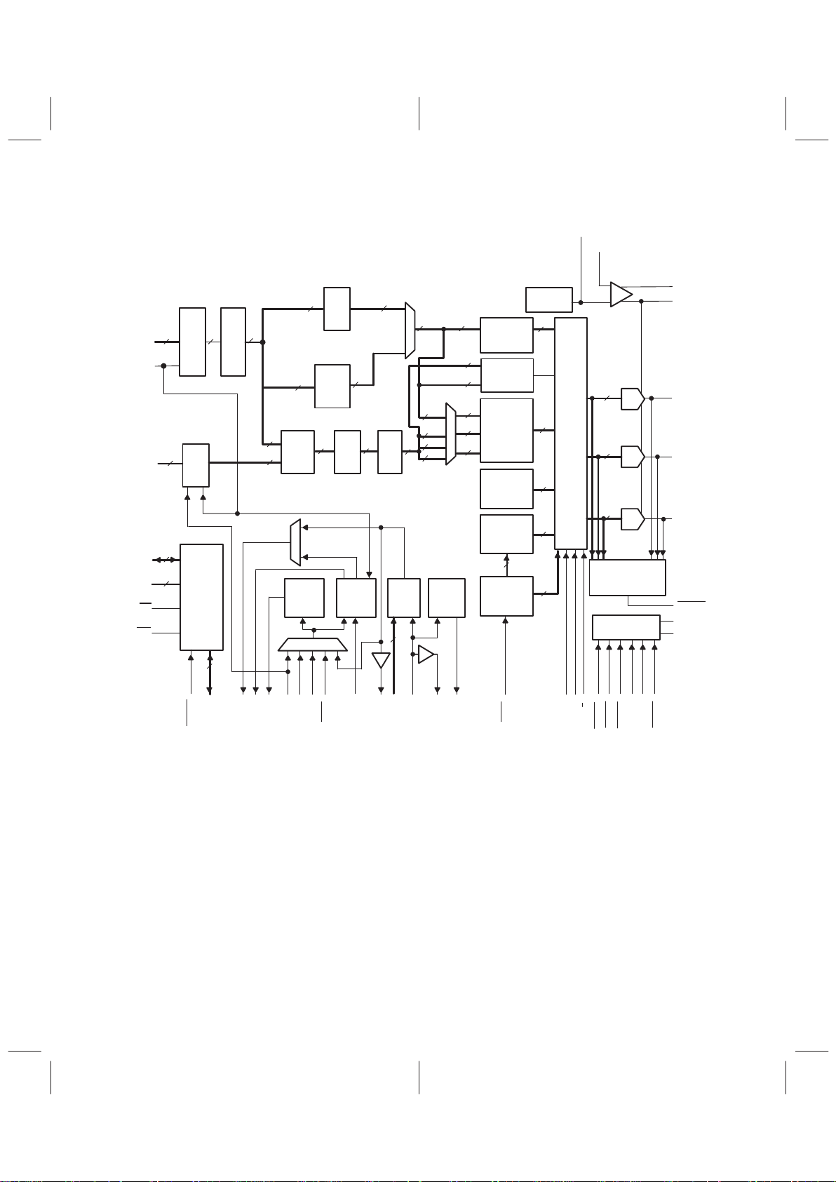
1.2 Functional Block Diagram
Clock Select
24
8
Pixel
Bus
Latch
1:1
2:1
Pipe
MUX
64
32
24
64
24 24 24
VGA
Latch
24
8
8
Read
Mask
8
Page
Reg
8
8
24
24
24
Output
MUX
DAC
8
8
8
DAC
DAC
V
ref
1.235 V
REF
FS ADJUST
COMP1
IOR
IOG
IOB
Test Function
and
Sense Comparator
Video-Signal
Control
SENSE
HSYNCOUT
VSYNCOUT
32
8
MPU
Registers
and
Control
Logic
8
5
5
P(63–0)
VGA(7–0)
D(7–0)
RS(3–0)
RD
WR
VGABL
VGAVS
VGAHS
SYSBL
SYSVS
SYSHS
PSEL
OVS
8/6
VCLK
SCLK
RCLK
PCLKOUT
SFLAG
CLK1
CLK0
GI/O(4–0)
RESET
COMP2
XTAL1
MCLK
8
8
8
8
Pseudo
Color
MUX
True
Color
MUX
Unpack
Logic
24
32
32
8
DOT
Clock
Divider
Loop
Clock
PLL
Pixel
Clock
PLL
Memory
Clock
PLL
2
2
2
ODD/EVEN
XTAL2
PLLSEL(1,0)
CLK2
CLK2
LCLK
Direct-Color
Pipeline
Delay
Color Key
Switch
3×256×8
Color
Palette
RAM
1×24
Overscan
Color
3×24
Cursor
Colors
64×64×2
Cursor RAM
and Control
Figure 1–1. Functional Block Diagram

1–4
1.3 Terminal Assignments
DD
DV
1
2
3
4
5
6
7
8
9
10
11
12
13
14
15
16
17
18
19
20
21
22
23
24
25
26
27
28
29
133
134
135
136
137
138
139
140
141
142
143
144
145
146
147
148
149
150
151
152
153
154
155
156
157
158
159
160
120
119
118
117
116
115
114
113
112
111
110
109
108
107
106
105
104
103
102
101
100
99
98
97
96
95
94
93
92
69
68
67
66
65
64
63
62
61
60
59
58
57
56
55
54
53
52
51
50
49
48
47
46
45
44
43
42
41
131
132
70
30
91
P33
P32
P31
P30
P29
P28
P27
P26
P25
P24
P22
P21
P20
GND
P19
P18
P17
P16
P15
P14
P13
P11
P10
P9
P8
123
124
125
126
127
128
129
130
121
122
79
78
77
76
75
74
73
72
71
80
32
33
34
35
36
37
38
39
90
89
88
87
86
85
84
83
82
40
81
P7
P6
P5
P4
P3
P1
P0
31
P12
P2
XTAL2
XTAL1
GND
DV
P57
P58
P59
P60
P61
P62
P63
CLK2
CLK2
CLK1
CLK0
SFLAG
VGABL
VGAVS
VGAHS
SYSBL
SYSVS
SYSHS
8/6
PSEL
OVS
VGA7
VGA6
VGA5
VGA4
VGA3
VGA2
VGA1
VGA0
AV
GND
AV
GND
GND
GND
DD
DD
DD
PLLSEL1
GND
P34
P35
P36
P37
P38
P39
P40
P41
P42
P43NCNC
PCLKOUT
PLLGND
P44
P45
P46
P47
GND
P48
P49
P50
P51
P52
P53
P54
P55
P56
SCLK
VCLK
RCLK
LCLK
ODD/EVEN
MCLK
PLLVDDPLLV
DD
DV
DD
GND
RS3
WR
RD
GND
D7D6D5D4D3D2D0
RS1
RS2
GI/O1
GI/O2
GI/O3
GI/O4
RESET
GND
HSYNCOUT
VSYNCOUT
GND
IOR
GND
IOG
GND
IOB
GND
FS ADJUST
COMP1
REF
COMP2
D1
RS0
GI/O0
SENSE
DV
DD
DV
DD
P23
PLLSEL0
NC – No internal connection
DD
DV
DD
DV
DD
DV
AV
DD
AV
DD
NC
Figure 1–2. Terminal Assignments
1–5
1.4 Ordering Information
TVP3026 – XXX XXXX
Pixel Clock Frequency Indicator
MUST CONTAIN THREE CHARACTERS:
–135: 135-MHz pixel clock (revision A only)
–175: 175-MHz pixel clock
–220: 220-MHz pixel clock
–250: 250-MHz pixel clock
Device Revision
MUST CONTAIN ONE LETTER:
A
B
Package
MUST CONTAIN THREE LETTERS:
PCE: Plastic, Quad Flat Pack
MDN:Metal, Quad Flat Pack
1.5 Terminal Functions
TERMINAL
NAME NO.
I/O
DESCRIPTION
AV
DD
80, 84,
86, 87
Analog power. All AVDD terminals must be connected. A separate cutout in the
DVDD plane should be made for AVDD. The DVDD and AVDD planes should be
connected only at a single point through a ferrite bead close to where power enters
the board.
CLK0 106 I Dot clock 0 TTL input. CLK0 can be selected to drive the dot clock at frequencies
up to 140 MHz. When using the VGA port, the maximum frequency is 85 MHz.
CLK0 can be selected as the latch clock for VGA data and video controls.
(power-up default).
CLK1 107 I Dot clock 1 TTL input. CLK1 can be selected to drive the dot clock at frequencies
up to 140 MHz.
CLK2, CLK2 108, 109 I Dual-mode dot clock input. These inputs are emitter-coupled logic
(ECL)-compatible inputs. Alternatively, CLK2 and CLK2
may be used as
individual TTL clock inputs. Programming the clock selection register selects the
chosen configuration. These inputs may be selected as the dot clock up to the
device limit while in the ECL mode or up to 140 MHz in the TTL mode.
COMP1,
COMP2
77, 79 I Compensation. COMP1 and COMP2 provide compensation for the internal
reference amplifier . A 0.1-µF ceramic capacitor is required between COMP1 and
COMP2. This capacitor must be as close to the device as possible to avoid noise
pick up.
DV
DD
2, 18, 39,
40, 45, 65,
117, 137
Digital power. All DVDD terminals must be connected to the digital power plane
with sufficient decoupling capacitors near the TVP3026.
D7–D0 47–54 I/O MPU interface data bus. Data is transferred in and out of the register map, palette
RAM, and cursor RAM on D7–D0.
NOTE 1: All unused inputs should be tied to a logic level and not allowed to float.
1–6
1.5 Terminal Functions (Continued)
TERMINAL
NAME NO.
I/O
DESCRIPTION
FS ADJUST 76 I Full-scale adjustment. A resistor connected between FS ADJUST and GND
controls the full-scale range of the DACs.
GND 17, 41, 46,
66, 69, 71,
73, 75,
81–83, 85,
118, 136,
159
Ground. All GND terminals must be connected. A common ground plane should
be used.
HSYNCOUT,
VSYNCOUT
67, 68 O Horizontal and vertical sync outputs. These outputs are pipeline delayed
versions of the selected sync inputs. Output polarity inversion may be
independently selected using general control register bits GCR(1,0).
IOR, IOG,
IOB
70, 72, 74 O Analog current outputs. These outputs can drive a 37.5-Ω load directly (doubly
terminated 75-Ω line), thus eliminating the requirement for any external buffering.
GI/O4–GI/O0 58–62 I/O Software programmable general I/O terminals that can be used to control
external devices.
LCLK 123 I Latch clock input. LCLK latches pixel-bus-input data and system video controls.
VGA data may also be latched with LCLK when selected. LCLK may be a delayed
version of RCLK provided that linear phase changes in RCLK cause
corresponding linear phase changes in LCLK.
MCLK 121 O Memory clock output. MCLK is the output of an independently programmable
PLL frequency synthesizer. The frequency range is 14 – 100 MHz. The dot clock
may be output on this terminal while the MCLK frequency is reprogrammed. See
subsection 2.4.2.1,
Changing the MCLK Frequency
.
PCLKOUT 144 O Pixel clock PLL output. PCLKOUT is a buffered version of the pixel clock PLL
output and is mainly for test purposes. This output is independent of the dot clock
source selected by the clock selection register.
PLLGND 142 Ground for PLL supplies. Decoupling capacitors should be connected between
PLLVDD and PLLGND. PLLGND should be connected to the system ground
through a ferrite bead.
PLLV
DD
143, 146 PLL power supply. PLLVDD must be a well regulated 5-V power supply voltage.
Decoupling capacitors should be connected between PLLVDD and PLLGND.
T erminal 143 supplies power to the pixel clock PLL. T erminal 146 supplies power
to the MCLK PLL and the loop clock PLL.
OVS 96 I Overscan input. OVS controls the display of custom screen borders. When OVS
is not used, it should be connected to GND.
ODD/EVEN 122 I Odd or even field display. ODD/EVEN indicates odd or even field during
interlaced display for cursor operation. A low signal indicates the even field and
a high signal indicates the odd field. See subsection 2.7.4,
Interlaced Cursor
Operation
, for cursor operation in interlace mode.
PLLSEL0,
PLLSEL1
1, 160 I Pixel clock PLL frequency selection. PLLSELx selects among two fixed
frequencies and the programmed frequency of the pixel clock PLL.
NOTE 1: All unused inputs should be tied to a logic level and not allowed to float.
1–7
1.5 Terminal Functions (Continued)
TERMINAL
NAME NO.
I/O
DESCRIPTION
PSEL 97 I Port select. PSEL provides the capability of switching between direct color and
true color or overlay. Multiple true color or overlay windows may be displayed
using the PSEL control. Since PSEL is sampled with LCLK, the granularity for
switching depends on the number of pixels loaded per LCLK. When PSEL is not
used, it should be connected to GND.
P63–P0 3–16,
19–38,
110 –116,
127–135,
138–141,
149–158
I Pixel input port. The port can be used in various modes as described in
Section 2.6, Multplexing Modes of Operation. Unused terminals should not be
allowed to float.
RCLK 124 O Reference clock output. RCLK can be programmed to output either the pixel clock
PLL (power up default) or the loop clock PLL. The pixel clock PLL is selected to
provide a reference clock to the VGA controller. In this configuration, the VGA
controller returns VGA data and video controls along with a synchronous clock
which becomes the TVP3026 dot clock source using CLK0. For all other modes,
the loop clock PLL is selected to provide the reference clock. In this configuration,
the pixel clock PLL (or external clock) becomes the TVP3026 dot clock source.
The reference clock is used to generate VRAM shift clocks (or clocks a VGA
controller) and generate video controls. The pixel port (or VGA port) and video
controls are latched by LCLK. The loop clock PLL controls the phase of RCLK to
phase-lock the received LCLK with the internal dot clock.
For systems that use SCLK as the VRAM shift clock, RCLK should be connected
to LCLK. An external buffer may be used between RCLK and LCLK when SCLK
is also buffered, within the timing constraints of the TVP3026. RCLK is not gated
off during blanking.
REF 78 I/O Voltage reference for DACs. An internal voltage reference of nominally 1.235 V
is provided that requires an external 0.1-µF ceramic capacitor between REF and
analog GND. However, the internal reference voltage can be overdriven by an
externally-supplied reference voltage.
RESET 63 I Master reset. All the registers assume their default state after reset. The default
state is VGA mode 2 (CLK0 latching of VGA data and video controls).
RD 44 I Read strobe input. A low signal on RD initiates a read from the register map. Read
transfer data is enabled onto the D(7–0) bus when RD
is low (see
Figure 3–1).
RS3–RS0 42, 55–57 I Register select inputs. These terminals specify the location in the direct register
map that is to be accessed as shown in Table 2–1.
SCLK 126 O Shift clock output. SCLK is a gated version of the loop clock PLL output and is
gated off during blanking. SCLK may drive the VRAM shift clock directly. This is
intended for designs in which the graphics controller does not supply the VRAM
shift clock.
SENSE 64 O Test mode DAC comparator output signal. SENSE is low when one or more of the
DAC output analog levels is above the internal comparator reference of
350 mV ±50 mV .
NOTE 1: All unused inputs should be tied to a logic level and not allowed to float.
1–8
1.5 Terminal Functions (Continued)
TERMINAL
NAME NO.
I/O
DESCRIPTION
SFLAG 105 I Split shift register transfer flag. A high pulse on SFLAG during blanking is passed
directly to the SCLK terminal. This operation is available to meet the special serial
clocking requirements of some VRAM devices. When SFLAG is not used,
SFLAG should be connected to GND.
SYSBL 101 I System blank input. SYSBL is active low. This should be selected for all modes
other than VGA mode 2. This signal is pipeline delayed before being passed to
the DACs.
SYSHS,
SYSVS
99, 100 I System horizontal and vertical sync inputs. These signals should be selected for
all modes other than VGA mode 2. These signals are pipeline delayed and each
may be inverted before being passed to the HSYNCOUT and VSYNCOUT
terminals. General control register bits GCR(1,0) control the polarity inversion.
When used to generate the sync level on the green current output, SYSHS
and
SYSVS
must be active low at the input to the TVP3026.
VCLK 125 O Programmable auxiliary clock output. VCLK is derived from the internal dot clock
using a programmable divide ratio and does not utilize the loop clock PLL for
synchronization. Since pixel data and video controls are always referenced to
RCLK and LCLK (or CLK0), use of VCLK for the frame buffer interface or video
timing is not recommended.
VGABL 104 I VGA blank input. VGABL is active low. This should be selected when in VGA
mode 2 (CLK0 latching of VGA data and video controls). VGABL
is pipeline
delayed before being passed to the DACs.
VGAHS,
VGAVS
102, 103 I VGA horizontal and vertical sync inputs. These signals should be used when in
VGA mode 2 (CLK0 latching of VGA data and video controls). These signals are
pipeline delayed and each may be inverted before being passed to the
HSYNCOUT and VSYNCOUT terminals. General control register bits GCR(1,0)
control the polarity inversion. When used to generate the sync level on the green
current output, VGAHS and VGAVS must be active low at the input to the
TVP3026.
VGA7 –VGA0 88 –95 I VGA port. This bus can be selected as the pixel input bus for VGA modes, but
it does not allow for any multiplexing.
WR 43 I Write strobe input. A low signal on WR initiates a write to the register map. Write
transfer data is latched from the D(7–0) bus with the rising edge of WR
.
XTAL1,
XTAL2
119, 120 I/O Connections for quartz crystal resonator. XTALx is a reference for the frequency
synthesis PLLs. XTAL2 may be used as a TTL reference clock input, in which
case XTAL1 is left unconnected.
8/6 98 I DAC resolution selection. This terminal is used to select the data bus width (8 or
6 bits) for the DACs and is provided for VGA downward compatibility . When the
8/6
signal is high, 8-bit bus transfers are used with D7 the MSB and D0 the LSB.
For 6-bit bus operation, while the color palette RAM still has the 8-bit information,
the data is shifted to the upper six bits and the two LSBs are filled with zeros at
the output multiplexer to the DACs. The palette RAM data register zeroes the two
MSBs when the palette RAM is read in the 6-bit mode. The function of this
terminal may be overridden in software. When not used, the 8/6
terminal should
be connected to GND so that 6-bit VGA operation begins at power up.
NOTE 1: All unused inputs should be tied to a logic level and not allowed to float.
2–1
2 Detailed Description
2.1 Microprocessor Unit Interface
The standard microprocessor unit (MPU) interface is supported, giving the MPU direct access to the
registers and memories of the TVP3026. The processor interface is controlled using read and write strobes
(RD
, WR), four register select terminals (RS3–RS0), the D7–D0 data terminals, and the 8/6-select terminal.
The 8/6
terminal is used to select between an 8- or 6-bit-wide data path to the color palette RAM and is
provided to maintain compatibility with the IMSG176. See subsection 2.1.1,
8/6 Operation
.
Table 2–1 lists the direct register map. These registers are addressed directly by the register select lines
RS0–RS3. Table 2–2 lists the indirect register map. The index for the indirect register map is loaded into
the index register (direct register: 0000). This register also stores the palette RAM write address and cursor
RAM write address. The indexed data register (direct register: 1010) is then used to read or write the register
pointed to in the indirect register map. The index does not post-increment following accesses to the indirect
map.
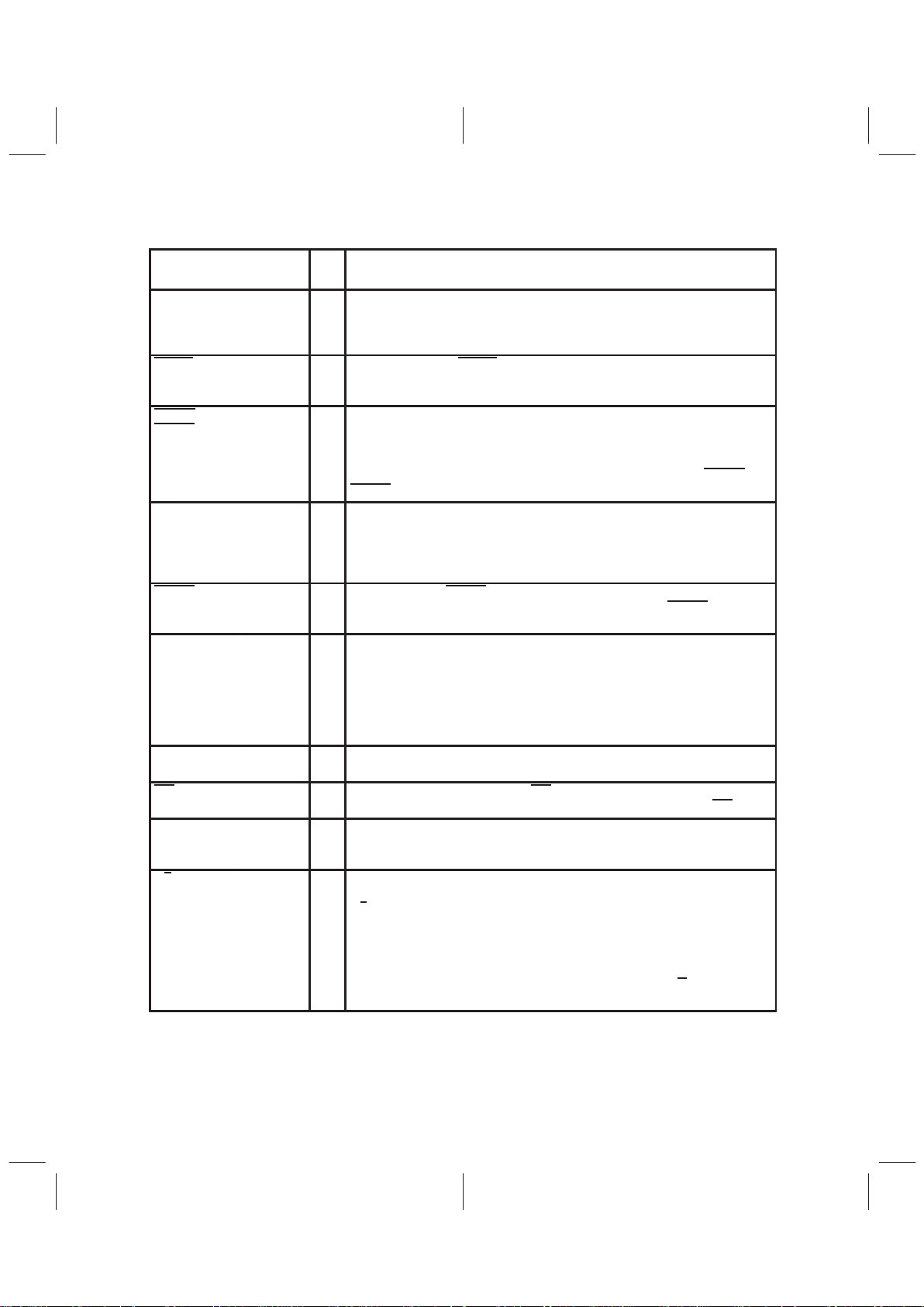
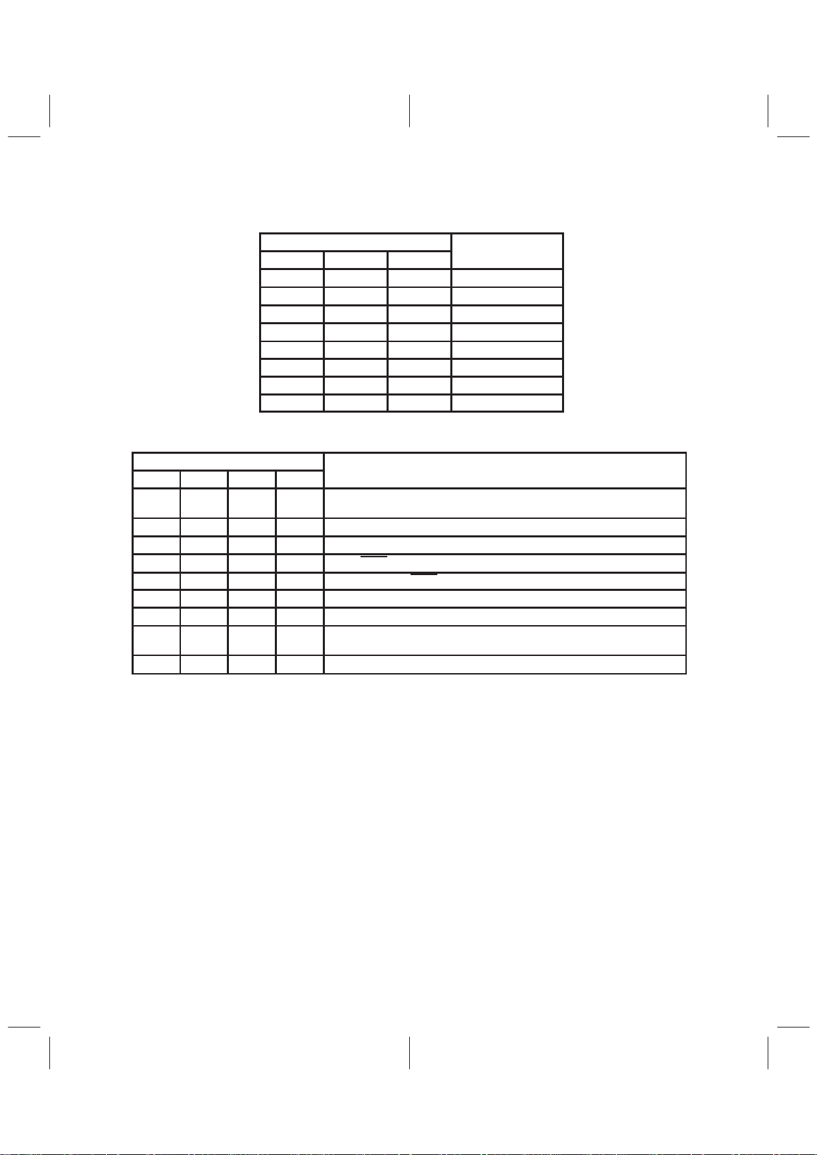
Table 2–1. Direct Register Map
RS3 RS2 RS1 RS0 REGISTER ADDRESSED BY MPU R/W DEFAULT (HEX)
0 0 0 0
Palette/Cursor RAM Write Address/
Index Register
R/W XX
0 0 0 1 Palette RAM Data R/W XX
0 0 1 0 Pixel Read-Mask R/W FF
0 0 1 1 Palette/Cursor RAM Read Address R/W XX
0 1 0 0 Cursor/Overscan Color Write Address R/W XX
0 1 0 1 Cursor/Overscan Color Data R/W XX
0 1 1 0 Reserved
0 1 1 1 Cursor/Overscan Color Read Address R/W XX
1 0 0 0 Reserved
1 0 0 1 Direct Cursor Control R/W 00
1 0 1 0 Indexed Data R/W XX
1 0 1 1 Cursor RAM Data R/W XX
1 1 0 0 Cursor-Position X LSB R/W XX
1 1 0 1 Cursor-Position X MSB R/W XX
1 1 1 0 Cursor-Position Y LSB R/W XX
1 1 1 1 Cursor-Position Y MSB R/W XX

2–2
Table 2–2. Indirect Register Map (Extended Registers)
INDEX R/W DEFAULT
REGISTER ADDRESSED
BY INDEX REGISTER
0x00 Reserved
0x01 R 0x00
†
Silicon Revision
0x02–0x05 Reserved
0x06 R/W 0x00 Indirect Cursor Control
0x07–0x0E Reserved
0x0F R/W 0x06 Latch Control
0x10–0x17 Reserved
0x18 R/W 0x80 True Color Control
0x19 R/W 0x98 Multiplex Control
0x1A R/W 0x07 Clock Selection
0x1B Reserved
0x1C R/W 0x00 Palette Page
0x1D R/W 0x00 General Control
0x1E R/W 0x00 Miscellaneous Control
0x1F–0x29 Reserved
0x2A R/W 0x00 General-Purpose I/O Control
0x2B R/W XX General-Purpose I/O Data
0x2C R/W XX PLL Address
0x2D R/W XX Pixel Clock PLL Data
0x2E R/W XX Memory Clock PLL Data
0x2F R/W XX Loop Clock PLL Data
0x30 R/W XX Color-Key Overlay Low
0x31 R/W XX Color-Key Overlay High
0x32 R/W XX Color-Key Red Low
0x33 R/W XX Color-Key Red High
0x34 R/W XX Color-Key Green Low
0x35 R/W XX Color-Key Green High
0x36 R/W XX Color-Key Blue Low
0x37 R/W XX Color-Key Blue High
0x38 R/W 0x00 Color-Key Control
0x39 R/W 0x18 MCLK/Loop Clock Control
0x3A R/W 0x00 Sense Test
0x3B R XX Test Mode Data
0x3C R XX CRC Remainder LSB
†
Silicon revision register is 0x00 for the first pass silicon (see subsection 2.11.4,
Silicon Revision
).
NOTE 1: Reserved registers should be avoided; otherwise, circuit behavior could
deviate from that specified.
2–3
Table 2–2. Indirect Register Map (Extended Registers) (Continued)
INDEX R/W DEFAULT
REGISTER ADDRESSED
BY INDEX REGISTER
0x3D R XX CRC Remainder MSB
0x3E W XX CRC Bit Select
0x3F R 0x26 ID
0xFF W XX Software Reset
NOTE 1: Reserved registers should be avoided; otherwise, circuit behavior
could deviate from that specified.
2.1.1 8/6 Operation
The 8/6 terminal is used to select between an 8-bit (set to 1) or 6-bit (reset to 0) data path to the color palette
RAM and it is provided in order to maintain compatibility with the INMOS IMSG176. When
miscellaneous-control register bit 2 (MSC2) is set to 1, the 8/6
terminal is disabled and 8/6 operation is
controlled by bit 3 of the miscellaneous-control register (MSC3). The reset default is for the 8/6
terminal to
be enabled (miscellaneous-control register bit 2 = 0, see Section 2.2,
Color Palette RAM
).
2.1.2 Pixel Read-Mask Register
The pixel read-mask register (direct register: 0010) is an 8-bit register used to enable or disable a bit plane
from addressing the color-palette RAM in the pseudo-color and VGA modes. Each palette address bit is
logically ANDed with the corresponding bit from the read-mask register before going to the palette-page
register and addressing the palette RAM.
2.1.3 Palette-Page Register
The palette page register (index: 0x1C) allows selection of multiple color look-up tables stored in the palette
RAM when using a mode that addresses the palette RAM with less than 8 bits. When using 1, 2, or 4 bit
planes in the pseudo-color or direct-color + overlay modes, the additional planes are provided from the page
register before the data addresses the color palette. This is illustrated in Table 2–3.
NOTE
The additional bits from the page register are inserted after the read mask.
The palette-page register specifies the additional bit planes for the overlay field in
direct-color modes with less than 8 bits per pixel overlay.
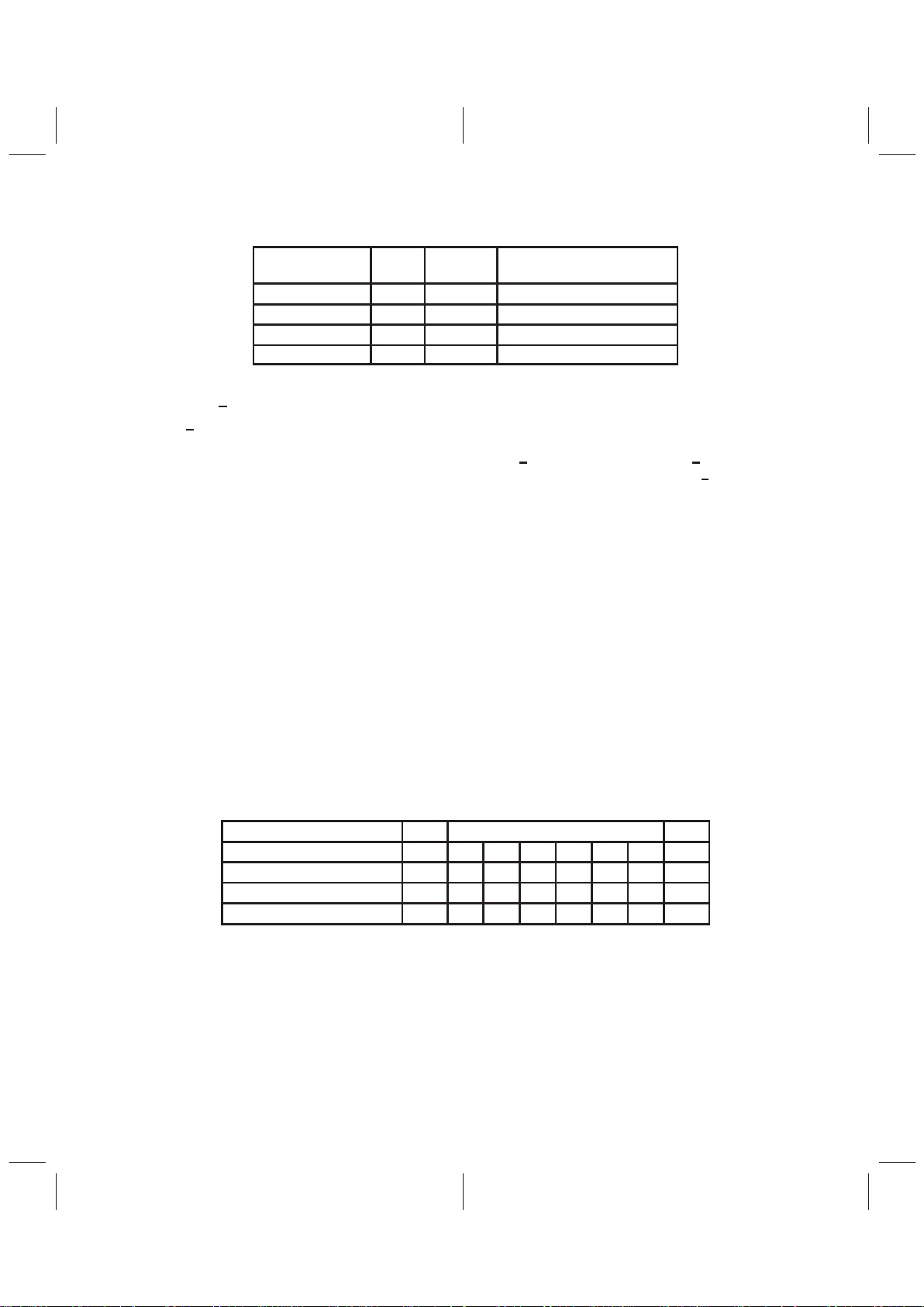
Table 2–3. Allocation of Palette-Page Register Bits
NUMBER OF BIT PLANES MSB PALETTE ADDRESS BITS LSB
8 M M M M M M M M
4 P7 P6 P5 P4 M M M M
2 P7 P6 P5 P4 P3 P2 M M
1 P7 P6 P5 P4 P3 P2 P1 M
M = bit from pixel port and Pn = n bit from page register.
2–4
2.1.4 Cursor and Overscan Color Registers
The registers for the three cursor colors and the overscan border color are accessed through the direct
register map. See Section 2.9,
Overscan Border
description and subsection 2.7.3,
Three-Color 64 X 64
Cursor
, for use of the cursor colors.
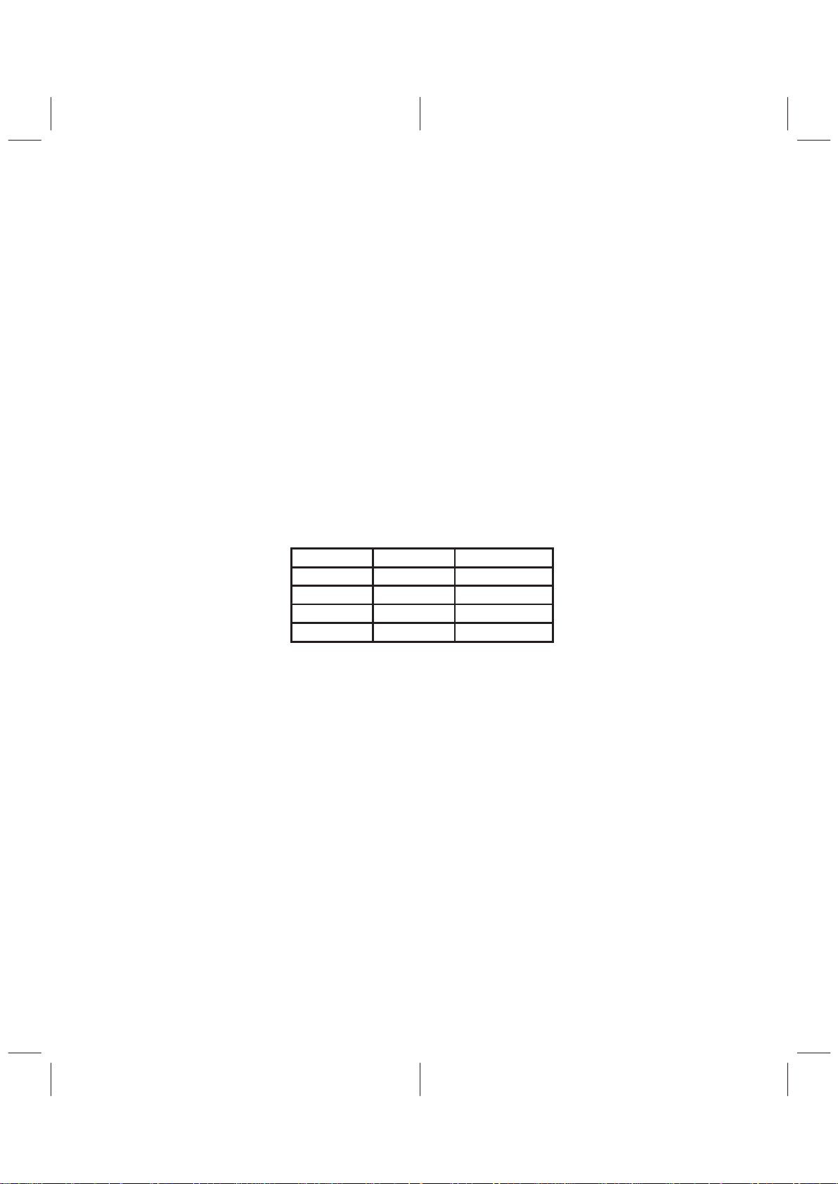
The color write address register (direct register: 0100) must be initialized before writing to the color registers.
The lower two bits of this register select one of the four color registers according to T able 2–4. The selected
24-bit color register is loaded a byte at a time by writing a sequence of three bytes (red, green, and blue)
to the color data register (direct register: 0101). After the blue byte is written, the color address register
increments to the next color. All four colors may be loaded with a single write to the color write address
register followed by 12 consecutive writes to the color data register.
The color read address register (direct register: 0111) must be initialized before reading from the color
registers. The lower two bits of this register select one of the four color registers according to T able 2–4. Next,
the color data register (direct register: 0101) is read three times, producing red, green, and blue bytes from
the selected register. After the blue byte is read, the color address register is incremented to the next color .
All four colors may be read with a single write to the color read address register followed by 12 consecutive
reads of the color data register.
The sequence followed by the color address register is overscan color, cursor color 0, cursor color 1, cursor
color 2, . . ., etc. The starting point depends on what was written to the color write address or color read
address register.
Table 2–4. Color Register Address Format
BIT 1 BIT 0 REGISTER
0 0 Overscan color
0 1 Cursor color 0
1 0 Cursor color 1
1 1 Cursor color 2
2.2 Color-Palette RAM
The color-palette RAM is addressed by an internal 8-bit address register for reading/writing data from/to the
RAM. This register is automatically incremented following a RAM transfer, allowing the entire palette to be
read/written with only one access of the address register. When the address register increments beyond
the last location in RAM, it is reset to the first location (address 0). All read and write accesses to the RAM
are asynchronous to the internal clocks but are performed within one dot clock. Therefore, read/write
accesses do not cause any noticeable disturbance on the display.
The color palette RAM is 24 bits wide for each location and 8 bits wide for each color. Since a MPU access
is 8 bits wide, the color data stored in the palette is eight bits when the 6-bit mode is chosen. When the 6-bit
mode is chosen, the two MSBs of color data in the palette have the values previously written. However, when
they are read back in the 6-bit mode, the two MSBs are zeros to be compatible with INMOS IMSG176 and
Brooktree Bt176. The output multiplexer shifts the six LSB bits to the six MSB positions and fills the two LSBs
with 0s after the color palette. The multiplexer then feeds the data to the DAC. The test mode data register
and the cyclic redundancy check (CRC) calculation both take data after the output multiplexer, enabling total
system verification. The color palette access is described in the following two sections, and it is fully
compatible with IMSG176/8 and Bt476/8.

2–5
2.2.1 Writing to Color-Palette RAM
To load the color palette, the MPU must first write to the color-palette RAM write address register (direct
register: 0000) with the address where the modification is to start. The selected color-palette RAM location
is loaded a byte at a time by writing a sequence of three bytes (red, green, and blue) to the palette RAM data
register (direct register: 0001). After the blue write cycle, the color-palette RAM address register increments
to the next location, which the MPU may modify by simply writing another sequence of red, green, and blue
data.
2.2.2 Reading From Color-Palette RAM
Reading from the color-palette RAM is performed by writing to the palette read address register (direct
register: 0011) with the location to be read. Three successive MPU reads from the palette RAM data register
produce red, green, and blue color data (6 or 8 bits depending on the 8/6
mode) for the specified location.
Following the blue read cycle, the address register is incremented. Since the color-palette RAM is dual
ported, the RAM may be read during active display without disturbing the video.
2.3 Clock Selection
The TVP3026 VIP provides a maximum of four clock inputs (CLK0, CLK1, and CLK2/CLK2) which can be
selected as two TTL inputs and a differential ECL input or as four TTL inputs. The TTL inputs can be used
for video rates up to 140 MHz while the differential ECL can be utilized up to the device limit. At reset, CLK0
is selected as the clock source for VGA mode 2. This power-up state supports VGA pass through operation
without requiring software intervention.
An alternative clock source can be selected in the clock-selection register (index: 0x1A) during normal
operation. This chosen clock input is then used as the dot clock (representing pixel rate to the monitor, see
Table 2–5).
There are two ways of using CLK0 as a clock source. When CSR(2–0) = 11 1, CLK0 is selected as the clock
source to generate the internal dot clock (see T able 2–6). In this mode, multiplex control register bit MCR6
must be set to 1 and only the VGA port can be used. This selects latching of VGA(7–0) and VGABL
with
CLK0. When CSR(2–0) = 000, CLK0 is also selected as the clock source to generate the internal dot clock.
However, in this mode, MCR6 must be logic 0, which selects latching of VGA(7–0) and SYSBL
with LCLK.
In this mode, the pixel port or the VGA port can be used.
Additionally , two crystal oscillator terminals (XT AL1, XTAL2) are provided for the integrated pixel clock and
memory clock frequency synthesis PLLs. These terminals are intended for use with a quartz crystal
resonator, but a discrete oscillator can also be utilized and input on the XTAL2 terminal (XTAL1 terminal
should be left floating in this case).
Selection of the pixel clock PLL as the pixel clock source is performed by programming the clock selection
register. In general, when the pixel clock PLL is to be selected, it should be selected after the PLL has been
programmed and allowed to achieve lock.
2–6
Table 2–5. Clock-Selection Register Bits CSR(6–4)
(Index: 0x1A, Access: R/W, Default: 0x07)
CLOCK-SELECT REGISTER BITS
6 5 4
VCLK FREQUENCY
0 0 0 Dot clock
0 0 1 Dot clock/2
0 1 0 Dot clock/4
0 1 1 Dot clock/8
1 0 0 Dot clock/16
1 0 1 Dot clock/32
1 1 0 Dot clock/64
1 1 1 Reset to 0
NOTE 2: Bit CSR7 enables the SCLK output when set to 1.
Table 2–6. Clock-Selection Register Bits CSR(3–0) (Index: 0x1A, Access: R/W, Default: 0x07)
CLOCK SELECT REGISTER BITS
3 2 1 0
FUNCTION
0 0 0 0 Select CLK0 as clock source (for use with LCLK latching of VGA port). See
subsection 2.6.2,
VGA Modes
.
0 0 0 1 Select CLK1 as clock source
0 0 1 0 Select CLK2 as TTL clock source
0 0 1 1 Select CLK2 as TTL clock source
0 1 0 0 Select CLK2 and CLK2 as ECL clock source
0 1 0 1 Select pixel clock PLL as clock source
0 1 1 0 Disable internal dot clock for reduced power consumption.
0 1 1 1 Select CLK0 as clock source (for use with CLK0 latching of VGA port). See
subsection 2.6.2,
VGA Modes
.
1 X X X Reserved
x = do not care
2.4 PLL Clock Generators
In addition to externally supplied clock sources, the TVP3026 has three on-chip, fully programmable,
frequency-synthesis phase-locked loops (PLLs). The first PLL ,pixel clock, is intended for pixel clock
generation for frequencies up to the device limit. The second PLL ,MCLK, is provided for general system
clocking such as the system clock or memory clock, and the third PLL ,called the loop clock PLL, is useful
for synchronizing pixel data and latch timing by compensating for system loop delay.
The clock generators use a modified M over (N × 2
P
) scheme to enable a wide range of precise frequencies.
(Appendix A provides a listing of all frequencies that can be synthesized and the register values for each.)
The advanced PLLs utilize an internal loop filter to provide maximum noise immunity and minimum jitter.
Except for the reference crystal or oscillator, no external components or adjustments are necessary. Each
PLL can be independently enabled or disabled for maximum system flexibility. Figure 2–1 illustrates the
TVP3026 PLL clocking scheme. The PLLs are programmed through a group of four registers in the
TVP3026 indirect register map. The registers are listed in Table 2–7.
2–7
Table 2–7. PLL Top Level Registers
INDEX REGISTER
0x2C PLL address register (PAR)
0x2D Pixel clock PLL data register (PPD)
0x2E MCLK PLL data register (MPD)
0x2F Loop clock PLL data register (LPD)
The PLL address register (PAR) points to the M, N, P, and status registers of each PLL. This register allows
read and write access and contains three 2-bit pointers, one for each PLL, according to the T able 2–8. Each
pointer may be programmed independently .
Table 2–8. PLL Address Register
(Index: 0x2C, Access: R/W, Default: Uninitialized)
PAR BITS POINTER
1–0 Pixel clock PLL data register pointer
3–2 MCLK PLL data register pointer
5–4 Loop clock PLL data register pointer
Each PLL data register pointer directs its associated PLL to one of its four PLL registers according to
Table 2–9.
Table 2–9. PLL Data Register Pointer Format
BIT 1 BIT 0 REGISTER
0 0 N-value register
0 1 M-value register
1 0 P-value register
1 1 Status register (read-only)
Once the PLL data register pointers are set, the selected register is accessed through the pixel clock PLL
data register (index: 0x2D), MCLK PLL data register (index: 0x2E) or the loop clock PLL data register (index:
0x2F). The PLL data register pointer bits are independently autoincremented following a write cycle to the
corresponding PLL data register. The current state of each pointer can be identified by reading the PLL
address register (index: 0x2C). The PLL data register pointer bits do not autoincrement following a read
cycle of the PLL data registers.
The most efficient way to program the pixel clock PLL is to first write zeros to PLL address register bits
PAR(1,0) followed by three consecutive writes to the pixel clock PLL data register to program the N, M, and
P-value registers. Following the third write, the pixel clock PLL pointer will point to the read-only status
register. The status register can then be polled until the LOCK bit is set (the pointer does not autoincrement
on reads). For test purposes, the pixel clock PLL can be output on the PCLKOUT terminal by setting the
pixel clock PLL P-value register bit 6 to 1.
2–8
Loop
Clock PLL
VCLK
Divider
Pixel Clock
PLL
MCLK
PLL
Crystal
Amplifier
RCLK
VCLK
MCLK
Internal
Dot Clock
CLK0–2/2
XTAL2
XTAL1
PCLKOUT
LCLK
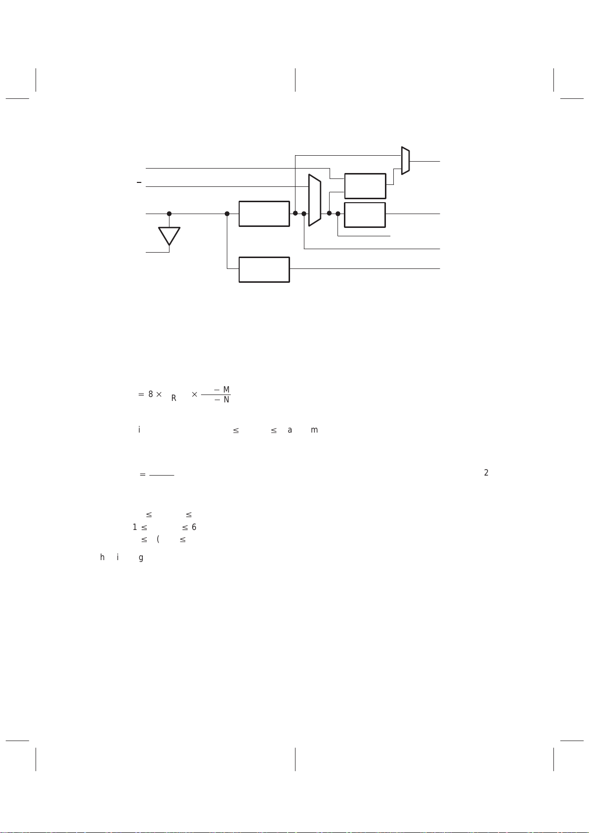
Figure 2–1. TVP3026 Clocking Scheme
2.4.1 Pixel Clock PLL
The pixel clock PLL may be used at frequencies up to the device limit. Appendix A provides optimal register
values for all frequencies that can be synthesized using the common 14.31818 MHz reference. The
following equations describe the voltage controlled oscillator frequency and the PLL output frequency for
the pixel clock PLL as a function of the N, M, and P values and the reference frequency F
REF
.
The frequency of the voltage controlled oscillator (VCO) is given by:
Provided:
F
VCO
+8
F
REF
65*M
65*N
Minimum VCO FrequencyvF
V
CO
v
Maximum VCO Frequency
(1)
Then the PLL output frequency is :
F
PLL
+
F
VCO
2
P
(2)
The N-, M-, and P-value registers may be programmed to any value within the following limits:
40vN(5–0)v62
1vM(5–0)v62
0vP(1,0)v3
The bit assignments of the N-, M-, and P-value and the status register for the pixel clock PLL are given in
Table 2–10. The bits shown as set to 0 or 1 must be written with these fixed values. PCLKEN enables the
pixel clock PLL output onto the PCLKOUT output terminal when set to 1. When PCLKEN is reset to 0, the
PCLKOUT terminal is held at 0. PLLEN resets the PLL to 0 and enables the PLL to oscillate when set to
1. When PFORCE is set to 1, the pixel clock PLL uses its programmed N, M, and P registers and ignores
PLLSEL(1,0). When LFORCE is set to 1, the loop clock PLL uses its programmed N, M, and P registers and
ignores PLLSEL(1,0). The LOCK status bit indicates that the PLL has locked to the selected frequency when
set to 1. The remaining status register bits are for test purposes.
2–9
Table 2–10. Pixel Clock PLL Registers
REGISTER BIT 7 BIT 6 BIT 5 BIT 4 BIT 3 BIT 2 BIT 1 BIT 0
N value 1 1 N5 N4 N3 N2 N1 N0
M value 0 0 M5 M4 M3 M2 M1 M0
P value PLLEN PCLKEN 1 1 LFORCE PFORCE P1 P0
Status X LOCK X X X X X X
X = do not care
2.4.1.1 Pixel Clock PLL Frequency Selection
The pixel clock PLL frequency may be selected using the PLL select inputs PLLSEL(1,0) as shown in
Table 2–11. The first two selections are fixed frequency settings for standard VGA operation. Use of a
standard 14.31818 MHz crystal is assumed. When PLLSEL1 is set to 1, the frequency specified by the pixel
clock PLL N-, M-, and P-value registers is selected. When PLLSEL1 is set to 1 at power up or during a
software reset, the pixel clock PLL N-, M-, and P-value registers default to settings for 25.057 MHz, but with
the PLL disabled. Therefore, the system must reset PLLSEL(1,0) to 0x when a software reset occurs or the
pixel clock PLL and RCLK stops oscillating.
The frequency select inputs also apply to the loop clock PLL. When a fixed frequency is selected
(PLLSEL(1,0) = 0x), the loop clock PLL passes the dot clock frequency to the RCLK multiplexer. Internal
feedback is used, no external signal path from RCLK to LCLK is required. When PLLSEL1 is 1, the frequency
specified by the loop clock PLL N-, M-, and P-value registers is selected.
For VGA Mode 1, the pixel clock PLL is normally selected as the dot clock source (CSR = 0x05) and the
RCLK terminal passes the loop clock PLL output (MCK5 = 1). Then, when PLLSEL(1,0) changes between
a programmed frequency and a fixed frequency, the loop clock PLL automatically changes with it. The loop
clock PLL does not require reprogramming.
For VGA Mode 2, CLK0 should be selected as the dot clock source (CSR = 0x07) and the RCLK terminal
should pass the pixel clock PLL output (MCK5 = 0). In this case, the loop clock PLL should be disabled (bit
P7 = 0) since its output is not used.
Table 2–11. Pixel Clock PLL Frequency Selection
PLLSEL1 PLLSEL0 PIXEL CLOCK PLL FREQUENCY LOOP CLOCK PLL FREQUENCY
0 0 25.057 MHz Pass DOT CLOCK, internal feedback
0 1 28.636 MHz Pass DOT CLOCK, internal feedback
1 X Programmed by pixel clock PLL registers Programmed by loop clock PLL registers
X = do not care
2–10
2.4.2 Memory Clock PLL
The memory clock (MCLK) PLL may be used at frequencies up to 100 MHz. Appendix A provides optimal
register values for all frequencies that can be synthesized using the common 14.31818 MHz reference. The
MCLK PLL maximum output frequency of 100 MHz may not be exceeded. The equations for the VCO
frequency and for the PLL output frequency are the same as for the pixel clock PLL.
Provided:
F
VCO
+8
F
REF
65*M
65*N
Minimum VCO FrequencyvF
V
CO
v
Maximum VCO Frequency
(3)
Then the PLL output frequency is :
F
PLL
+
F
VCO
2
P
(4)
The N-, M-, and P-value registers may be programmed to any value within the following limits:
40vN(5–0)v62
1vM(5–0)v62
0vP(1,0)v3
The bit assignments of the N-, M-, and P-value and the status register for the MCLK PLL are given in
Table 2–12. The bits shown as 0 or 1 must be written with these fixed values. PLLEN resets the PLL with
0 and enables the PLL to oscillate when set to 1. When set to 1, the LOCK status bit indicates that the PLL
has locked to the selected frequency. The remaining status register bits are for test purposes. The MCLK
PLL and loop clock PLL are further controlled by the MCLK/loop clock control register shown in T able 2–13.
Table 2–12. MCLK PLL Registers
REGISTER BIT 7 BIT 6 BIT 5 BIT 4 BIT 3 BIT 2 BIT 1 BIT 0
N value 1 1 N5 N4 N3 N2 N1 N0
M value 0 0 M5 M4 M3 M2 M1 M0
P value PLLEN 0 1 1 0 0 P1 P0
Status X LOCK X X X X X X
X = do not care
2–11
Table 2–13. MCLK/Loop Clock Control Register (Index: 0x39 hex, Access: R/W, Default: 0x18)
BIT NAME VALUES DESCRIPTION
MKC7 0 Reserved
MKC6,
MKC5
00: Pixel clock PLL
(default)
01: Loop clock PLL
10: Dot clock /N
11: Reserved
Selects signal to output on RCLK terminal. Pixel clock PLL is selected as
default to support VGA mode 2. In VGA mode 2, the graphics accelerator
receives RCLK and returns its VGA output clock to the CLK0 terminal
along with synchronous VGA data. Select loop clock PLL for all modes
using LCLK data latching. The dot clock /N option provides the output of
the loop clock PLL N prescaler. This signal is a low pulse, one dot clock
wide, with a repetition rate of F
REF
/ (65–N).
MKC4 0: Dot clock
1: MCLK PLL (default)
MKC4 selects the signal to output on MCLK terminal. MCLK PLL is
selected as default. Select dot clock to ensure a stable output on MCLK
while MCLK PLL frequency is reprogrammed. See subsection 2.4.2.1,
Changing the MCLK Frequency
. A change of this bit does not take effect
until MKC3 bit transitions from 0 to 1. During this transistion, the MKC4
bit should not be changed.
MKC3 0:
1: (default)
Strobe for MCLK terminal output multiplexer control (MKC4). A 0 to 1
transition of this bit strobes in bit MKC4, causing bit MKC4 to take effect.
While MKC3 is transitioning from 0 to 1, MKC4 should not be changed.
MKC2, MKC1,
MKC0
000: Divide by 2 (default)
001: Divide by 4
010: Divide by 6
011: Divide by 8
100: Divide by 10
101: Divide by 12
110: Divide by 14
111: Divide by 16
Loop clock PLL post scalar Q divider. This additional frequency division
is applied after the 2P division of the loop clock PLL P-value register. For
a binary value of Q in MKC2–MKC0, the resulting frequency division is
2*(Q+1).
After the device resets, the MCLK PLL outputs a 50.11 MHz clock frequency and the pixel clock PLL output
depends on the PLLSEL1 and PLLSEL0 inputs according to Table 2–11. These frequencies assume a
standard 14.31818 MHz crystal reference. The actual output frequencies are proportional to the reference
frequency used.
2.4.2.1 Changing the MCLK Frequency
The MCLK is normally used as the graphics controller system clock and memory clock. During
reprogramming of the PLLs, a wide range of unpredictable frequencies are generated as the PLL transitions
to the new programmed frequency . These transition effects can produce unwanted results in some systems.
The TVP3026 provides a mechanism for smooth transitioning of the MCLK PLL. The following programming
steps are recommended.
1. Disable the pixel clock PLL (PLLEN bit = 0). Program the pixel clock PLL N, M, and P registers
(with PLLEN bit = 1) to the same frequency to which MCLK is to be changed. Poll the pixel clock
PLL status until the LOCK bit is set to 1.
2. Select the pixel clock PLL as the dot clock source if it is not already selected.
3. Switch to output dot clock on the MCLK terminal by writing bits MKC4 and MKC3 to 0,0 followed
by 0,1 in the MCLK/loop clock control register.
4. Disable the MCLK PLL (PLLEN bit = 0). program the MCLK PLL N, M, and P registers (with
PLLEN bit = 1) for the new frequency. Poll the MCLK PLL status until the LOCK bit is set to 1.
5. Switch to output MCLK on the MCLK terminal by writing bits MKC4 MKC3 to 1,0 respectively,
followed by 1,1 respectively in the MCLK/loop clock control register.
2–12
6. Disable the pixel clock PLL (PLLEN bit = 0). Program the pixel clock PLL N, M, and P registers
(with PLLEN bit = 1) for the original operating pixel frequency. Poll the pixel clock PLL status until
the LOCK bit is set to 1.
2.4.3 Loop Clock PLL
Many of the current high performance graphics accelerators with built in VGA support prefer to generate
their own VRAM shift clock and pixel data latching clock (LCLK) as discussed in subsection 2.5.2,
Frame-Buffer Timing Without Using SCLK
. As stated before, the TVP3026 provides an RCLK timing
reference output to be used by the graphics controller to generate these signals. A common industry
problem exists, however, in that the delay through the loop (i.e., from RCLK through the controller to produce
LCLK and pixel data) may be greater than the RCLK cycle time minus setup time. It then becomes very
difficult to resynchronize the rising edges of the LCLK signal to the internal dot clock within the specified
timing requirements. V ariations in graphics accelerator propagation delays from device to device can cause
severe production problems at the board level. The TVP3026 incorporates a unique loop clock PLL circuit
to maintain a valid LCLK/dot clock phase relationship and ensure that proper LCLK and pixel data setup
timing is met, regardless of the amount of system loop delay.
After device reset, the loop clock PLL provides the dot clock frequency to the RCLK output multiplexer.
However, the RCLK output multiplexer will ignore the loop clock PLL output and instead pass the pixel clock
PLL output to the RCLK terminal, which provides a reference clock to the VGA controller. In this configuration
(VGA mode 2), the VGA controller returns VGA data and video controls along with a synchronous clock that
becomes the TVP3026 dot clock source using CLK0. The PLLSEL(1,0) lines select either the 25.057 MHz
or 28.636 MHz VGA frequencies.
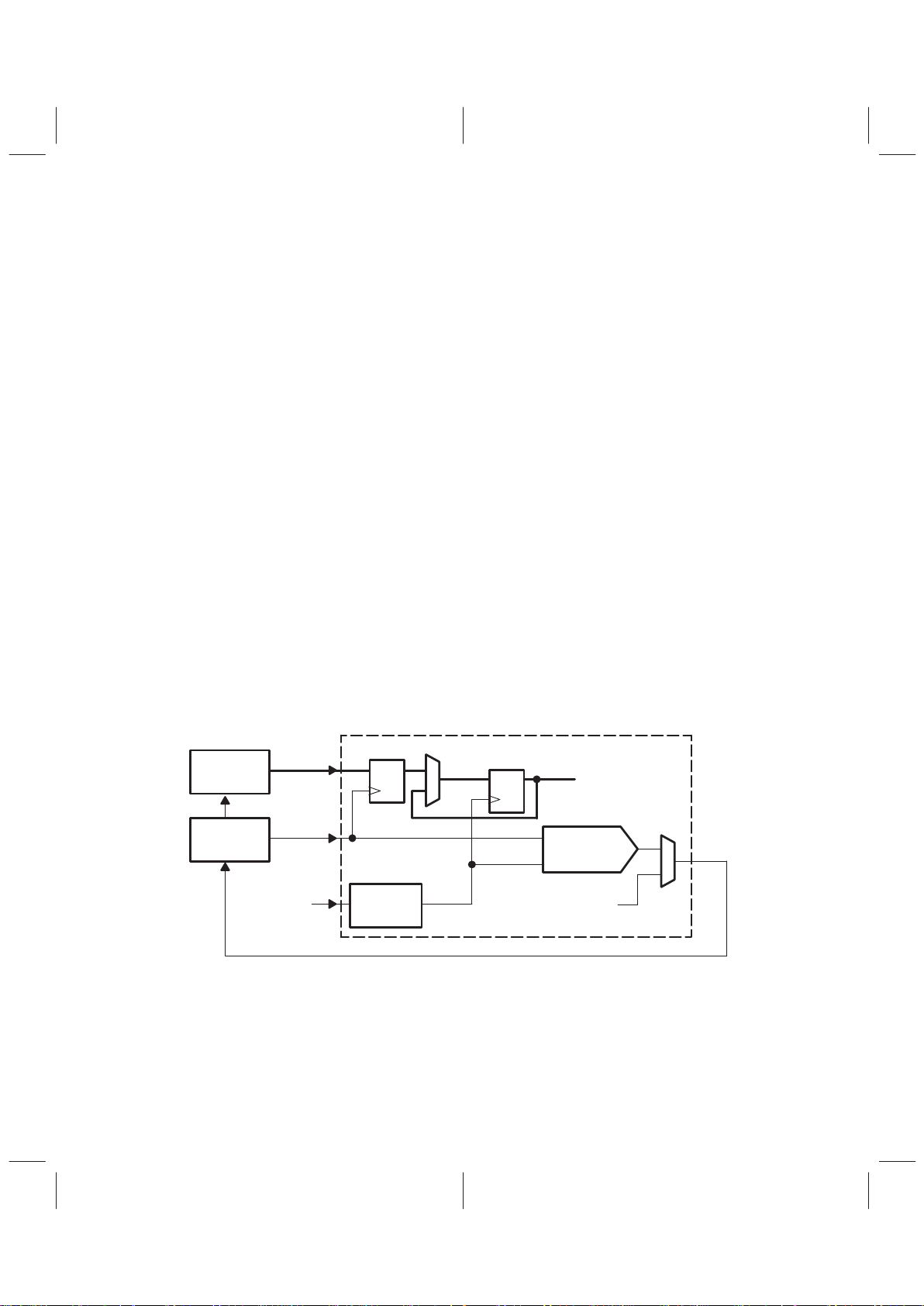
Figure 2–2 illustrates the pixel data latching structure and the operation of the loop clock PLL. The selected
clock source generates the dot clock which drives most of the digital logic of the TVP3026. The dot clock
is used as a reference frequency by the loop clock PLL and is subdivided as specified by the N value register.
The incoming LCLK is used as the other input of the PLL and is subdivided as specified by the M value
register. The PLL generates RCLK with the proper frequency and phase shift to phase align the divided dot
clock and divided LCLK. The pixel bus is latched on the rising edge of LCLK and then aligned with the internal
dot clock to synchronize with internal logic.
Loop Clock
PLL
DQ
DQ
LCLK
Dot Clock
Generator
Dot
Clock
Input Data Latch Structure
TVP3026
RCLK
CLKx
LCLK
P(63–0)
Graphics
Accelerator
VRAM
From Pixel Clock PLL
Figure 2–2. Loop Clock PLL Operation
The bit assignments of the N-, M-, and P-value and the status register for the loop clock PLL are shown in
Table 2–14. The bits shown as 0 or set to 1 must be written with these fixed values. When cleared to 0,
PLLEN disables the PLL and when set to 1, enables the PLL to oscillate. When reset to 1,the LOCK status
bit indicates that the PLL has locked to the selected frequency. The remaining status register bits are for
test purposes.
2–13
The N-, M-, and P-value registers may be programmed to any value within the following limits.
1vN(5–0)v62
1vM(5–0)v62
0vP(1,0)v3
LESEN enables the LCLK edge synchronizer function and should be set to 1 whenever a packed-24 mode
is used. In the packed-24 modes, only one LCLK rising edge per pixel group is aligned with the internal dot
clock. For example, in 8:3 packed-24 mode, only one of the three LCLKs is aligned to the internal dot clock.
The LCLK edge synchronizer function allows selection of which LCLK edge in the sequence of pixel bus
words is aligned with the internal dot clock. For each packed-24 mode there is an optimum setting for the
LCLK edge synchonizer delay LES1 and LES0. See Table 2–15 and subsection 2.6.6,
Packed-24 Mode
,
for more details.
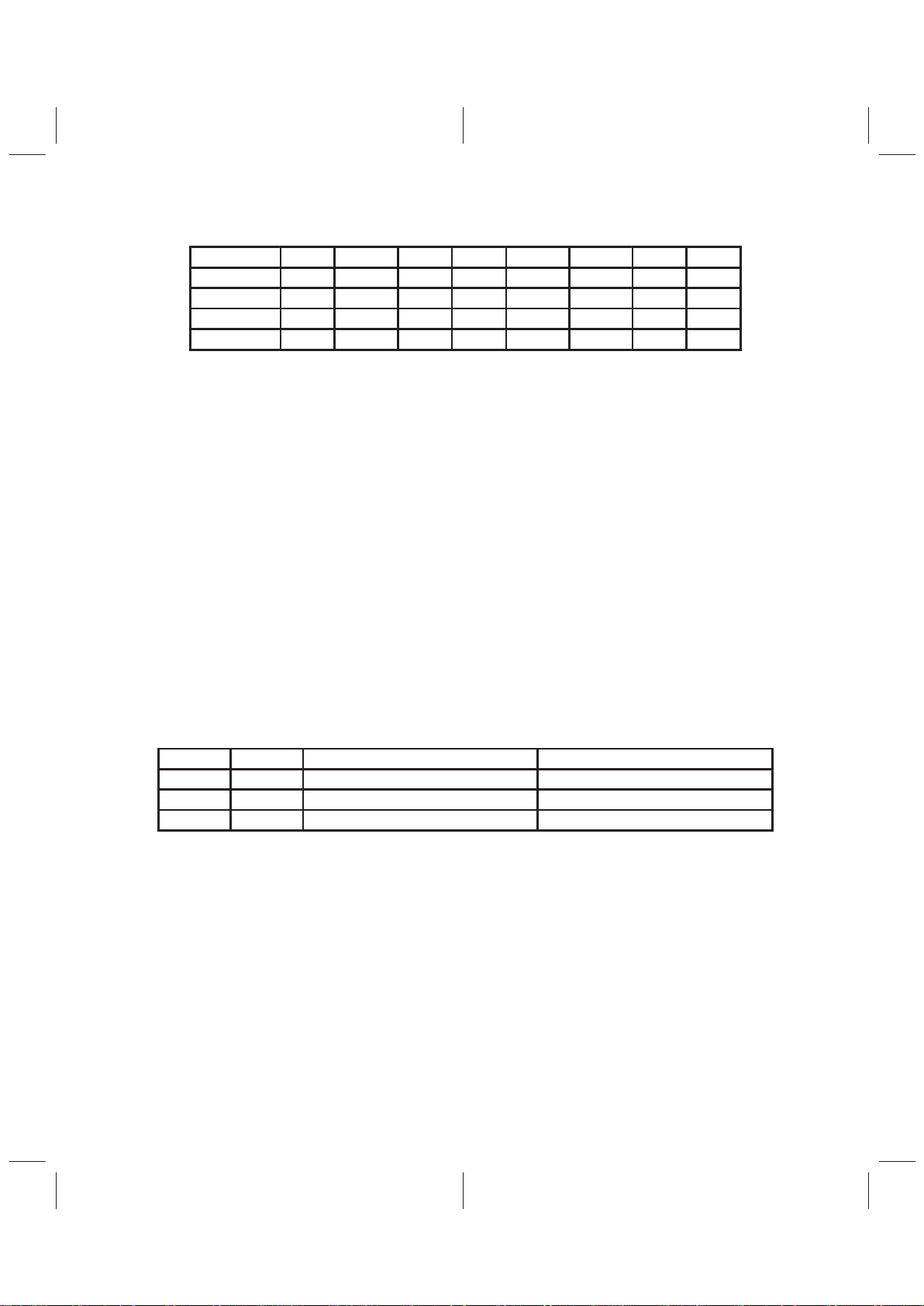
Table 2–14. Loop Clock PLL Registers
REGISTER BIT 7 BIT 6 BIT 5 BIT 4 BIT 3 BIT 2 BIT 1 BIT 0
N value 1 1 N5 N4 N3 N2 N1 N0
M value LES1 LES0 M5 M4 M3 M2 M1 M0
P value PLLEN 1 1 1 LESEN 0 P1 P0
Status X LOCK X X X X X X
X = do not care
2.4.3.1 Programming for All Modes Except Packed-24
For all modes except packed-24, programming of the loop clock PLL registers depends on the system
configuration, pixel rate, color depth and pixel bus width. In addition, the internal VCO must be within its
operating range of 1 10 MHz to 220 MHz for the required RCLK output frequency. To determine the proper
M, N, P, and Q register values one should know the following:
• Dot clock frequency (MHz) (F
D
) – pixel rate
• Bits/pixel (B) – bits/pixel including overlay fields
• Pixel bus width (W) – total pixel bus width used for this mode
• External division factor (K) – external frequency division between RCLK output and LCLK input
The dot clock frequency can either be generated by the on-chip pixel clock PLL or by an external clock
source. The following two parameters can be easily calculated from the above parameters.
• LCLK frequency (MHz) (F
L
) – frequency at which the pixel bus is loaded by the TVP3026
• RCLK frequency (MHz) (F
R
) – frequency at RCLK output terminal of TVP3026
The LCLK frequency is given by
FL+
FD
B
W
(5)
The RCLK frequency is FL times the external divide factor. When no external divide factor, K = 1.
FR+K
FL+K
FD
B
W
(6)
The N and M values are set as follows:
N+65*4
W
B
M+61
The P and Q frequency dividers must be programmed so that the VCO is within its operating range. The
VCO frequency is post-scaled by the P-divider followed by the Q-divider. The P-divider register (P) can take
2–14
on values of 0, 1, 2, or 3 which correspond to division factors of 1, 2, 4, or 8. The Q-divider register (Q) is
stored in bits 2 – 0 of the MCLK/loop clock control register (index: 0x39) and can take on values of 0, 1, 2,
. . ., 7 which correspond to division factors of 2, 4, 6, . . ., 16. The total post-scalar frequency division factor
is:
Z+2
P)1
(Q)1)+
F
VCO
(65*N
)
4 F
D
K
(7)
Next, set F
VCO
to the lower limit of 110 MHz and solve for Z:
Z
+
27.5
(65*N
)
FD
K
(8)
Finally , determine the P and Q values:
IF Zv16 then P+TRUNC (log2Z), Q+0
IF Zu16 then P+3, Q+INT
ǒ
Z*16
16
Ǔ
)
1
Set bits 7,6 of the N-value register to 1,1 (default). Set LES1 and LES0 in the M-value register (bits 7,6) to
0,0 (default). Set bits 7–2 of the P-value register to 1111 00. This enables the PLL to oscillate and disables
the LCLK edge synchronizer function, which is only used for packed-24 modes. T o reset the PLL by resetting
bit 7 of the P-value register to 0.
2.4.3.2 Programming for Packed-24 Modes
For packed-24 modes, the loop clock PLL is programmed according to Table 2–15. The LCLK edge
synchronizer delay (M-value register bits 7 and 6) depends on whether the graphics accelerator is driving
the VRAM shift clock (true color control register bit TCR5 is cleared to 0) or the TVP3026 is driving the VRAM
shift clock (TCR5 = 1). See subsection 2.6.6,
Packed-24 Mode
, for a typical setup procedure for packed-24
modes. As shown in Table 2–15, a different setting is required for the M-value register in the 4:3 multiplex
mode depending on the silicon revision. Software can determine the silicon revision by reading the silicon
revision register at index 0x01 (a value ≤ 0x20 indicates revision A and ≥ 0x21 indicates revision B).
Table 2–15. Loop Clock PLL Settings for Packed-24 Mode
PACKED-24 MODE
BIT TCR5
(Index 0x18)
N-VALUE REGISTER
M-VALUE REGISTER
TVP3026A
M-VALUE REGISTER
TVP3026B
4:3 0 0xFD 0×BE 0x3E
8:3 0 0×F9 0×BE 0×BE
5:4 0 0×FC 0×3D 0×3D
5:2 0 0×FC 0×7F 0×7F
4:3 1 0×FD 0×3E 0×BE
8:3 1 0×F9 0×3E 0×3E
5:4 1 0×FC 0×BD 0×BD
5:2 1 0×FC 0×FF 0×FF
2–15
The latch-control register definition is listed in Table 2–16.
Table 2–16. Latch-Control Register (Index: 0x0F , Access: R/W, Default: 0x06)
BIT NAME VALUES DESCRIPTION
LCR7, LCR6 00 Reserved
0×06 All 1:1, 4:1, 8:1, and 16:1 multiplex modes.
0×07
All 2:1 multiplex modes.
8:3 packed-24 or
4:3 packed-24 (revision A)
0×08 4:3 packed-24 (revision B)
LCR5–LCR0
0×20 5:2 packed-24
0×1F 5:4 packed-24, ×1 horizontal zoom
0×1E 5:4 packed-24, ×2 horizontal zoom
0×1C 5:4 packed-24, ×4 horizontal zoom
0×18 5:4 packed-24, ×8 horizontal zoom
The P and Q frequency dividers must be programmed so that the VCO is within its operating range of 110
MHz to 220 MHz. The VCO frequency is post scaled by the P-divider followed by the Q-divider. The P-divider
register (P) can take on values of 0, 1, 2, or 3 which correspond to division factors of 1, 2, 4, or 8. The
Q-divider register (Q) is stored in bits 2 – 0 of the MCLK/loop clock control register (index: 0x39) and can
take on values of 0, 1, 2, . . ., 7 which correspond to division factors of 2, 4, 6, . . ., 16. The total post-scalar
frequency division factor is:
Z+2
P)1
(Q)1)+
F
VCO
FD
K
65*N
65*M
(9)
Next, set F
VCO
to the lower limit of 110 MHz and solve for Z:
Z
+
110
F
D
K
65*N
65*M
(10)
Finally , determine the P and Q values:
IF Zv16 then P+TRUNCǒlog2ZǓ,Q+0
IF Zu16 then P+3, Q+INT
ǒ
Z*16
16
Ǔ
)
1
Set bits 7–2 of the P-value register to 11 1 1 10. This enables the PLL to oscillate and enables the LCLK edge
synchronizer function. To reset the PLL, clear bit 7 of the P-value register to 0.
2.4.3.3 Typical Device Connection
After reset, the TVP3026 defaults to VGA mode 2 (VGA pass through mode, see subsection 2.6.2,
VGA
Modes
) as do other devices in the TVP302x family. The RCLK terminal outputs the pixel clock PLL frequency
which is selected by PLLSEL1 and PLLSEL0. CLK0 is selected as the clock source and the VGA port is
selected as well as VGABL
, VGAHS, and VGAVS and these are latched with CLK0. The MCLK PLL outputs
the default 50.11MHz clock frequency.
Figure 2–3 shows the typical device connection for a system with VRAM clocked by the graphics
accelerator. After power up, the pixel clock PLL is output on RCLK and this clock drives the graphics
accelerator’s VGA controller and video timing logic. The accelerator’s output clock is output synchronous
to the VGA data and is input to the TVP3026 CLK0 input as the dot clock source.
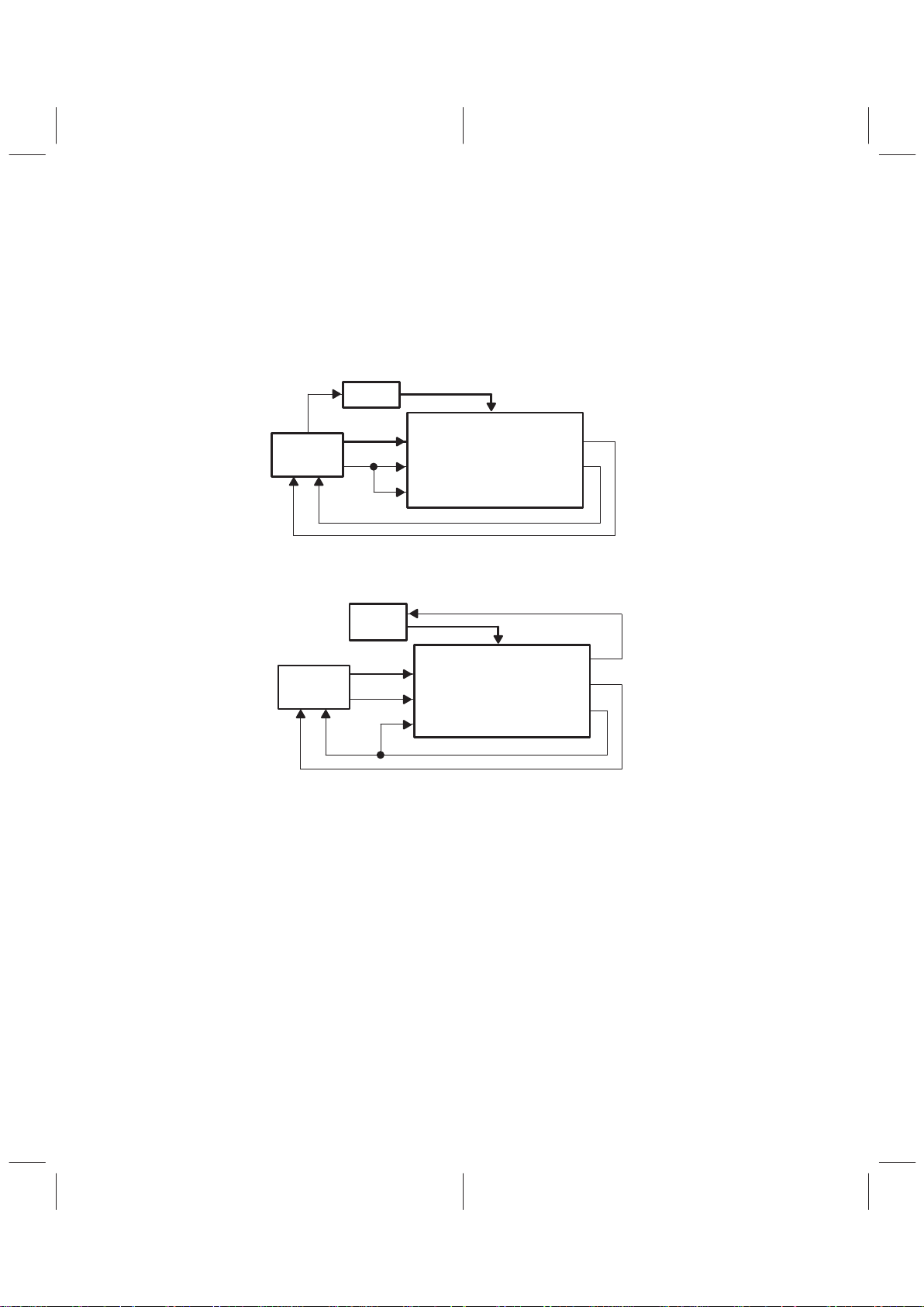
2–16
Figure 2–4 shows the typical device connection for a system with VRAM clocked by the TVP3026. In this
case, the RCLK is tied back to the LCLK and this same clock drives the graphics-accelerator VGA controller
and video timing logic. If necessary, the RCLK and SCLK signals may be externally buf fered within the timing
constraints (RCLK to LCLK delay) of the TVP3026. The pixel clock PLL is output on RCLK after power up.
For high resolution modes in both configurations, the pixel data is received from VRAM and the loop clock
PLL is used to adjust RCLK so that the received LCLK is aligned with the internal dot clock. The loop clock
PLL must be selected for output on the RCLK terminal. The pixel clock PLL (or an external clock source)
should be selected as the dot clock source.
Graphics
Accelerator
VRAM
VGA(7–0)
LCLK
CLK0
P(63–0)
MCLK
RCLK
TVP3026
Figure 2–3. Typical Configuration – VRAM Clocked by Accelerator
Graphics
Accelerator
VRAM
VGA(7–0)
LCLK
CLK0
P(63–0)
MCLK
RCLK
TVP3026
SCLK
Figure 2–4. Typical Configuration – VRAM Clocked by TVP3026
2.5 Frame-Buffer Interface
The TVP3026 provides two output clock signals and one input clock signal for controlling the frame-buffer
interface — SCLK, RCLK, and LCLK. The VCLK output is a division of the internal dot clock and has no
guaranteed phase relationship with RCLK. Therefore, VCLK should not be used for frame buffer interface
timing (pixel data and video controls). VCLK can drive general purpose external logic. Clocking of the frame
buffer interface is discussed in subsection 2.5.1,
Frame-Buffer Clocking
. The 64-bit pixel bus allows many
operational display modes as defined in Section 2.6,
Multiplexing Modes of Operation
, and T able 2–17. The
pixel latching sequence is initiated by a rising edge on LCLK. For those multiplexed modes in which multiple
pixels are latched on one LCLK rising edge, the pixel clock shifts the pixels out starting with the pixels that
reside on the low numbered pixel port terminals. For example, in an 8-bit-per-pixel pseudo-color mode with
an 8:1 multiplex ratio, the pixel display sequence is P(7 –0), P(15–8), P(23–16), P(31–24), P(39–32),
P(47–40), P(55–48), and P(63–56).
The TVP3026 frame-buffer interface also supports little- and big-endian data formats on the pixel bus. This
can be controlled by general-control register (GCR) bit 3. See subsection 2.6.1,
Little-Endian and
Big-Endian Data Format
, for details of operation.
 Loading...