


TUSB8040
USB 3.0 Four Port Hub
Data Manual
PRODUCTION DATA information is current as of publication date.
Products conform to specifications per the terms of the Texas
Instruments standard warranty. Production processing does not
necessarily include testing of all parameters.
Literature Number: SLLSE42
September 2010

TUSB8040
SLLSE42–SEPTEMBER 2010
www.ti.com
Contents
1 PRODUCT OVERVIEW ......................................................................................................... 5
1.1 Features ...................................................................................................................... 5
1.2 Introduction .................................................................................................................. 6
1.3 Functional Block Diagram .................................................................................................. 7
2 PIN DESCRIPTIONS ............................................................................................................. 8
2.1 Clock and Reset Signals ................................................................................................... 9
2.2 USB Upstream Signals ..................................................................................................... 9
2.3 USB Downstream Signals ................................................................................................ 10
2.4 I
2.5 Test and Miscellaneous Signals ......................................................................................... 11
2.6 Power Signals .............................................................................................................. 12
3 FUNCTIONAL DESCRIPTION ............................................................................................... 13
3.1 I
3.2 SMBus Slave Operation .................................................................................................. 13
3.3 Configuration Registers ................................................................................................... 14
4 CLOCK GENERATION ........................................................................................................ 21
4.1 Crystal Requirements ..................................................................................................... 21
4.2 Input Clock Requirements ................................................................................................ 21
5 POWER UP AND RESET ..................................................................................................... 22
6 ELECTRICAL SPECIFICATIONS (PRELIMINARY DATA) .......................................................... 23
6.1 ABSOLUTE MAXIMUM RATINGS ...................................................................................... 23
6.2 RECOMMENDED OPERATING CONDITIONS ....................................................................... 23
6.3 HUB INPUT SUPPLY CURRENT ....................................................................................... 23
2
C/SMBUS Signals ....................................................................................................... 11
2
C EEPROM Operation .................................................................................................. 13
3.3.1 ROM Signature Register ....................................................................................... 14
3.3.2 Vendor ID LSB Register ....................................................................................... 14
3.3.3 Vendor ID MSB Register ...................................................................................... 14
3.3.4 Product ID LSB Register ....................................................................................... 15
3.3.5 Product ID MSB Register ...................................................................................... 15
3.3.6 Device Configuration Register ................................................................................ 15
3.3.7 Battery Charging Support Register ........................................................................... 16
3.3.8 Device Removable Configuration Register .................................................................. 16
3.3.9 Port Used Configuration Register ............................................................................ 17
3.3.10 UUID Registers ................................................................................................. 17
3.3.11 Language ID LSB Register .................................................................................... 17
3.3.12 Language ID MSB Register ................................................................................... 18
3.3.13 Serial Number String Length Register ....................................................................... 18
3.3.14 Manufacturer String Length Register ........................................................................ 18
3.3.15 Product String Length Register ............................................................................... 19
3.3.16 Serial Number Registers ....................................................................................... 19
3.3.17 Manufacturer String Registers ................................................................................ 19
3.3.18 Product String Registers ....................................................................................... 20
3.3.19 Device Status and Command Register ...................................................................... 20
2 Contents Copyright © 2010, Texas Instruments Incorporated

TUSB8040
www.ti.com
SLLSE42–SEPTEMBER 2010
List of Figures
1-1 Typical Application................................................................................................................. 6
1-2 Functional Block Diagram ........................................................................................................ 7
4-1 TUSB8040 Clock ................................................................................................................. 21
Copyright © 2010, Texas Instruments Incorporated List of Figures 3

TUSB8040
SLLSE42–SEPTEMBER 2010
www.ti.com
List of Tables
2-1 Clock and Reset Signals.......................................................................................................... 9
2-2 USB Upstream Signals............................................................................................................ 9
2-3 USB Downstream Signals....................................................................................................... 10
2-4 I
2-5 Test and Miscellaneous Signals................................................................................................ 11
2-6 Power Signals .................................................................................................................... 12
3-1 TUSB8040 Register Map........................................................................................................ 13
3-2 Register Offset 0h................................................................................................................ 14
3-3 Bit Descriptions – ROM Signature Register .................................................................................. 14
3-4 Register Offset 1h................................................................................................................ 14
3-5 Bit Descriptions – Vendor ID LSB Register .................................................................................. 14
3-6 Register Offset 2h................................................................................................................ 14
3-7 Bit Descriptions – Vendor ID MSB Register ................................................................................. 14
3-8 Register Offset 3h................................................................................................................ 15
3-9 Bit Descriptions – Product ID MSB Register ................................................................................. 15
3-10 Register Offset 4h................................................................................................................ 15
3-11 Bit Descriptions – Product ID MSB Register ................................................................................. 15
3-12 Register Offset 5h................................................................................................................ 15
3-13 Bit Descriptions – Device Configuration Register ........................................................................... 15
3-14 Register Offset 6h................................................................................................................ 16
3-15 Bit Descriptions – Battery Charging Support Register ...................................................................... 16
3-16 Register Offset 7h................................................................................................................ 16
3-17 Bit Descriptions – Device Removable Configuration Register ............................................................. 16
3-18 Register Offset 8h................................................................................................................ 17
3-19 Bit Descriptions – Port Used Configuration Register ....................................................................... 17
3-20 Register Offset 10h-1Fh......................................................................................................... 17
3-21 Bit Descriptions – UUID Byte N Register ..................................................................................... 17
3-22 Register Offset 20h .............................................................................................................. 17
3-23 Bit Descriptions – Language ID LSB Register ............................................................................... 17
3-24 Register Offset 21h .............................................................................................................. 18
3-25 Bit Descriptions – Language ID LSB Register ............................................................................... 18
3-26 Register Offset 22h .............................................................................................................. 18
3-27 Bit Descriptions – Serial Number String Length Register .................................................................. 18
3-28 Register Offset 23h .............................................................................................................. 18
3-29 Bit Descriptions – Manufacturer String Length Register ................................................................... 18
3-30 Register Offset 24h .............................................................................................................. 19
3-31 Bit Descriptions – Product String Length Register .......................................................................... 19
3-32 Register Offset 30h-4Fh......................................................................................................... 19
3-33 Bit Descriptions – Serial Number Byte N Register .......................................................................... 19
3-34 Register Offset 50h-8Fh......................................................................................................... 19
3-35 Bit Descriptions – Manufacturer String Register ............................................................................ 19
3-36 Register Offset 90h-CFh ........................................................................................................ 20
3-37 Bit Descriptions – Product String Register ................................................................................... 20
3-38 Register Offset F8h .............................................................................................................. 20
3-39 Bit Descriptions – Device Status and Command Register ................................................................. 20
2
C/SMBUS Signals.............................................................................................................. 11
4 List of Tables Copyright © 2010, Texas Instruments Incorporated

TUSB8040
www.ti.com
SLLSE42–SEPTEMBER 2010
USB 3.0 Four Port Hub
Check for Samples: TUSB8040
1 PRODUCT OVERVIEW
1.1 Features
1
• USB 3.0 Compliant Four Port Hub, TID# 330000003
– Upstream Port Supports SuperSpeed, High-Speed and Full-Speed Connections
– Each of the Four Downstream Ports Support SuperSpeed, High-Speed, Full-Speed/Low-Speed
Connections
• USB 2.0 Hub Features
– Four Transaction Translators, One Per Port
– Four (Over USB Required Minimum of Two) Asynchronous Endpoint Buffers Per Transaction
Translator for Better Throughput
• Supports Charging Downstream Port (CDP) Applications
– Battery Charging 1.1 Compliant
• Supports Operation as a USB 3.0 or USB 2.0 Compound Device
• Supports Ganged Power Switching and Over-Current Protection
• Provides the following status outputs:
– High-Speed Operation
– High-Speed Upstream Port Suspended
– SuperSpeed Upstream Connection
– SuperSpeed Upstream Port Suspended
• Optional Serial EEPROM or SMBus Slave Interface for Custom Configurations:
– VID/PID
– Manufacturer and Product Strings
– UUID
– Serial Number
• Via EEPROM or SMBus Slave Interface, Each Downstream Port Can Be Independently:
– Enabled or Disabled
– Marked as Removable or Permanently Attached (for Compound Applications)
• Provides Unique 12-Hex-Character Serial Number String and 128-Bit Universally Unique Identifier
(UUID)
• Configurable SMBus Address to Support Multiple Devices on the Same SMBus Segment
• Supports On-Board and In-System EEPROM Programming Via the USB 2.0 Upstream Port
• Single Clock Input, 24-MHz Crystal or Oscillator
• Industrial Temperature Range, –40°C to 85°C
1
Please be aware that an important notice concerning availability, standard warranty, and use in critical applications of Texas
Instruments semiconductor products and disclaimers thereto appears at the end of this data sheet.
PRODUCTION DATA information is current as of publication date.
Products conform to specifications per the terms of the Texas
Instruments standard warranty. Production processing does not
necessarily include testing of all parameters.
Copyright © 2010, Texas Instruments Incorporated
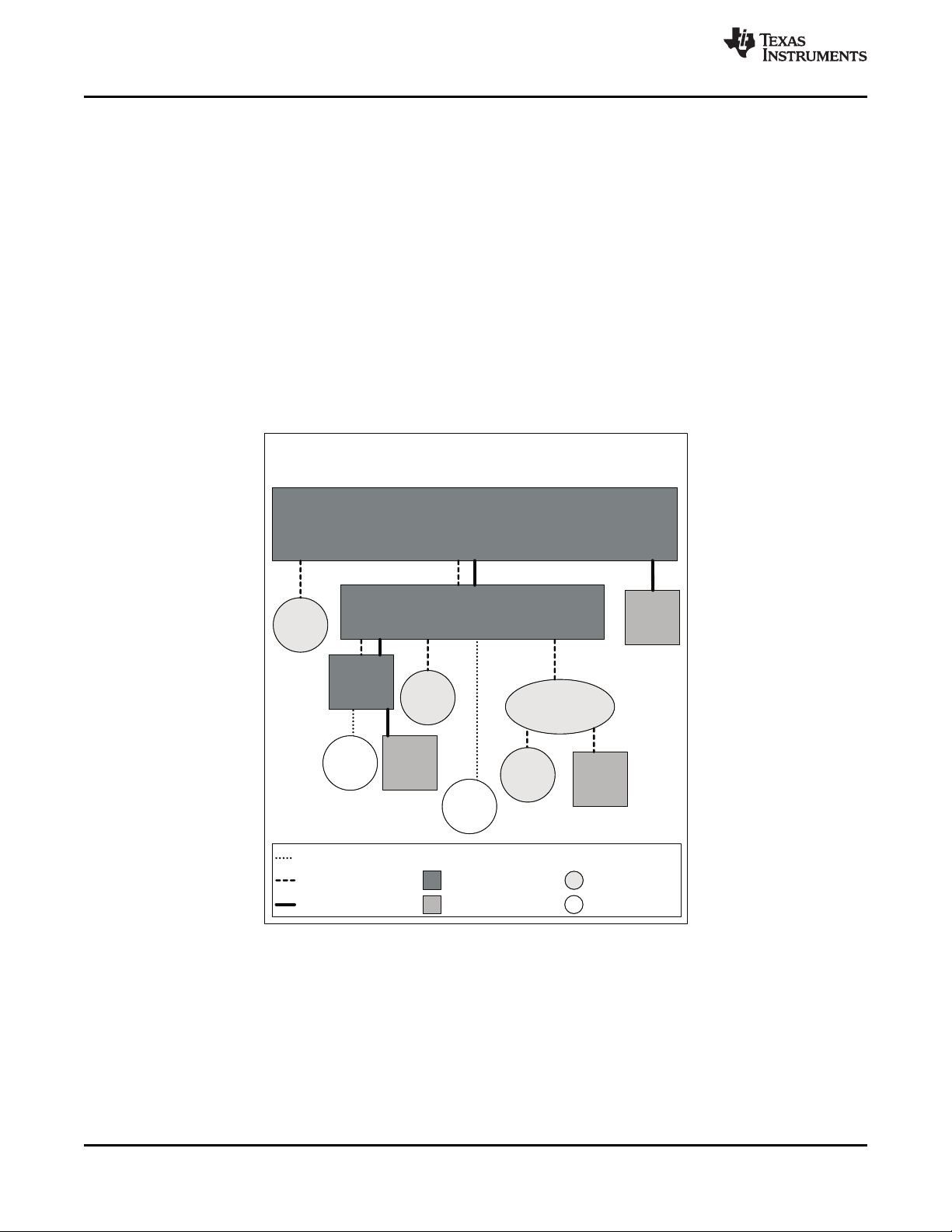
USB 3.0 Host Controller
USB 2.0
Device
USB 3.0
Device
TUSB8040
USB 3.0
Hub
USB 2.0 Hub
USB 3.0
Device
USB 2.0
Device
USB 2.0 Connection
USB 3.0 Connection
USB 2.0/3.0 Device
USB 3.0 Device
USB 2.0 Device
USB 3.0 System Implementation
USB 1.x Device
USB 2.0
Device
USB 3.0
Device
USB 1.1
Device
USB 1.1
Device
USB 1.x Connection
TUSB8040
SLLSE42–SEPTEMBER 2010
1.2 Introduction
The TUSB8040 is USB 3.0 compliant hub available in an 80-pin QFP package. The device is designed for
operation over the industrial temperature range of –40°C to 85°C.
The TUSB8040 provides simultaneous SuperSpeed and high-speed/full-speed connections on the
upstream port and provides SuperSpeed, high-speed, full-speed, or low-speed connections on the
downstream ports. When the upstream port is connected to an electrical environment that only supports
high-speed or full-speed/low-speed connections, SuperSpeed connectivity is disabled on the downstream
ports. When the upstream port is connected to an electrical environment that only supports
full-speed/low-speed connections, SuperSpeed and high-speed connectivity are disabled on the
downstream ports.
The TUSB8040 supports up to four downstream ports. It may be configured to report one to four
downstream ports by an attached EEPROM or SMBus controller. The configuration options provide the
ability to scale the device by application.
A typical system view of the TUSB8040 is shown in Figure 1-1.
www.ti.com
6 PRODUCT OVERVIEW Copyright © 2010, Texas Instruments Incorporated
Figure 1-1. Typical Application
Submit Documentation Feedback
Product Folder Link(s): TUSB8040
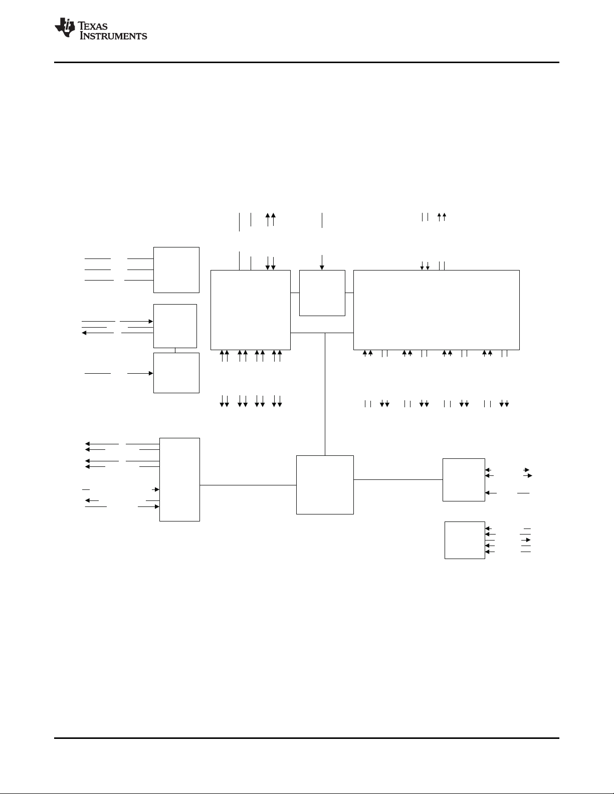
VBUS
Detect
SuperSpeed HubUSB 2.0 Hub
USB_DP_UP
USB_SSRXP_UP
USB_SSRXM_UP
USB_SSTXP_UP
USB_SSTXM_UP
USB_DM_UP
USB_SSRXP_DN0
USB_SSRXM_DN0
USB_SSTXP_DN0
USB_SSTXM_DN0
USB_SSRXP_DN1
USB_SSRXM_DN1
USB_SSTXP_DN1
USB_SSTXM_DN1
USB_SSRXP_DN2
USB_SSRXM_DN2
USB_SSTXP_DN2
USB_SSTXM_DN2
USB_SSRXP_DN3
USB_SSRXM_DN3
USB_SSTXP_DN3
USB_SSTXM_DN3
USB_DP_DN0
USB_DM_DN0
USB_DP_DN1
USB_DM_DN1
USB_DP_DN2
USB_DM_DN2
USB_DP_DN3
USB_DM_DN3
Oscilator
USB_R1
USB_R1RTN
USB_VBUS
XI
VSSOSC
XO
Clock
and
Reset
Distribution
Control
Registers
Boundary
Scan
Power
Distribution
JTAG_TRSTn
JTAG_TDI
JTAG_TDO
JTAG_TMS
JTAG_TCK
VDD33
VSS
GRSTz
I2C/
SMBUS
SCL/SMBCLK
SDA/SMDAT
SMBUSz
VDD11
GPIO
Block
PWRON0z_BATEN0
OVERCUR0z
SS
HS
HS_SUSPEND
SS_SUSPEND
FULLPWRMGMTz_SMBA1
TUSB8040
www.ti.com
1.3 Functional Block Diagram
The TUSB8040PFP is a reduced footprint hub that supports ganged power switching and over-current
protection. A ganged hub switches on power to all its downstream ports when power is required to be on
for any port. The power to the downstream ports is not switched off unless all ports are in a state that
allows power to be removed. Also when a ganged hub sense an over-current event, power to all
downstream ports will be switched off. It also provides customization using an I2C EEPROM or
configuration via an SMBus host for vendor specific PID, VID, and strings. Ports can also be marked as
disabled or permanently attached using an I2C EEPROM or an SMBus host.
The Device Status and Command Register at F8h cannot be modified by the contents of the I2C
EEPROM.
SLLSE42–SEPTEMBER 2010
Copyright © 2010, Texas Instruments Incorporated PRODUCT OVERVIEW 7
Figure 1-2. Functional Block Diagram
Submit Documentation Feedback
Product Folder Link(s): TUSB8040
40 OVERCUR0z
39 PWRON0z_BATEN0
38 VDD33
37 VDD11
36 SMBUSz
35 SDA_SMBDAT
34 SCL_SMBCLK
33 GRSTz
32 VDD11
31 JTAG_TDI
30 JTAG_RSTz
29 JTAG_TDO
28 JTAG_TMS
27 JTAG_TCK
26 VDD11
25 SS_SUSPEND
24 HS_SUSPEND
23 SS
22 HS
21 VDD33
40
39
38
37
36
35
34
33
32
31
30
29
28
27
26
25
24
23
22
21
VDD11
VDD11
USB_SSTXM_UP
USB_SSTXP_UP
USB_SSRXM_UP
USB_SSRXP_UP
VDD11
VDD33
USB_DM_UP
USB_DP_UP
VDD11
VDD33
USB_VBUS
XO
VSS_OSC
XI
VDD33
USB_R1
USB_R1RTN
VDD33
USB_DP_DN1
USB_DM_DN1
VDD33
VDD11
USB_SSTXM_DN1
USB_SSTXP_DN1
USB_SSRXM_DN1
USB_SSRXP_DN1
VDD11
VDD11
USB_SSTXM_DN3
USB_SSTXP_DN3
USB_SSRXM_DN3
USB_SSRXP_DN3
VDD11
USB_DP_DN3
USB_DM_DN3
VDD33
VDD11
FULLPWRMGMTz_SMBA1
60
59
58
57
56
55
54
53
52
51
50
49
48
47
46
45
44
43
42
41
61
62
63
64
65
66
67
68
69
70
71
72
73
74
75
76
77
78
79
80
VDD11
USB_DP_DN0
USB_DM_DN0
VDD33
VDD11
USB_SSRXP_DN0
USB_SSRXM_DN0
USB_SSTXP_DN0
USB_SSTXM_DN0
VDD11
VDD11
USB_SSRXP_DN2
USB_SSRXM_DN2
USB_SSTXP_DN2
USB_SSTXM_DN2
VDD11
USB_DP_DN2
USB_DM_DN2
VDD33
VDD11
1
2
3
4
5
6
7
8
9
10
11
12
13
14
15
16
17
18
19
20
Thermal Pad
PFP PACKAGE
(TOP VIEW)
TUSB8040
SLLSE42–SEPTEMBER 2010
2 PIN DESCRIPTIONS
www.ti.com
TYPE DESCRIPTION
I Input
O Output
I/O Input/output
PD, PU Internal pull-down/pull-up
PT Passive pass through
P Power Supply
G Ground
8 PIN DESCRIPTIONS Copyright © 2010, Texas Instruments Incorporated
Submit Documentation Feedback
Product Folder Link(s): TUSB8040

TUSB8040
www.ti.com
SLLSE42–SEPTEMBER 2010
2.1 Clock and Reset Signals
Table 2-1. Clock and Reset Signals
SIGNAL NAME TYPE PIN NO. DESCRIPTION
GRSTz I, PU 33 default states. When GRSTz is asserted, the device is completely nonfunctional. GRSTz
XI I 76 alternately be driven by the output of an external oscillator. When using a crystal a 1-MΩ
XO O 74 an external oscillator this pin may be left unconnected. When using a crystal a 1-MΩ
VSSOSC I 75 return path and it should not be connected to the PCB ground. If using an oscillator, this
Global power reset. This reset brings all of the TUSB8040 internal registers to their
should be asserted a minimum of 3 ms after all power rails are valid at the device.
Crystal input. This terminal is the crystal input for the internal oscillator. The input may
feedback resistor is required between XI and XO.
Crystal output. This terminal is crystal output for the internal oscillator. If XI is driven by
feedback resistor is required between XI and XO.
Oscillator return. If using a crystal, the load capacitors should use this signal as the
terminal should be connected to PCB Ground.
2.2 USB Upstream Signals
Table 2-2. USB Upstream Signals
SIGNAL NAME TYPE PIN NO. DESCRIPTION
USB_SSTXP_UP O 64 USB SuperSpeed transmitter differential pair (positive)
USB_SSTXM_UP O 63 USB SuperSpeed transmitter differential pair (negative)
USB_SSRXP_UP I 66 USB SuperSpeed receiver differential pair (positive)
USB_SSRXM_UP I 65 USB SuperSpeed receiver differential pair (negative)
USB_DP_UP I/O 70 USB high-speed differential transceiver (positive)
USB_DM_UP I/O 69 USB high-speed differential transceiver (negative)
USB_R1 PT 78
USB_R1RTN PT 79 Precision resistor reference return
USB_VBUS I 73 signal USB_VBUS must be connected to VBUS through a 90.9-KΩ ±1% resistor, and to
Precision resistor reference. A 10-KΩ ±1% resistor should be connected between
USB_R1 and USB_R1RTN.
USB upstream port power monitor. The VBUS detection requires a voltage divider. The
ground through a 10-KΩ ±1% resistor from the signal to ground.
Copyright © 2010, Texas Instruments Incorporated PIN DESCRIPTIONS 9
Submit Documentation Feedback
Product Folder Link(s): TUSB8040

TUSB8040
SLLSE42–SEPTEMBER 2010
2.3 USB Downstream Signals
Table 2-3. USB Downstream Signals
SIGNAL NAME TYPE PIN NO. DESCRIPTION
USB_SSTXP_DN0 O 8 USB SuperSpeed transmitter differential pair (positive)
USB_SSTXM_DN0 O 9 USB SuperSpeed transmitter differential pair (negative)
USB_SSRXP_DN0 I 6 USB SuperSpeed receiver differential pair (positive)
USB_SSRXM_DN0 I 7 USB SuperSpeed receiver differential pair (negative)
USB_DP_DN0 I/O 2 USB high-speed differential transceiver (positive)
USB_DM_DN0 I/O 3 USB high-speed differential transceiver (negative)
USB port power on control for downstream power/battery charging enable.
The terminal is used for control of the downstream power switch; in addition, the value
of the terminal is sampled at the de-assertion of reset to determine the value of the
battery charger support for the port as indicated in the Battery Charger Support register:
PWRON0z_BATEN0 I/O, PD 39 0 = Battery charging not supported
1 = Battery charging supported
The TUSB8040PFP only supports ganged mode. This terminal provides the port power
control for all downstream ports. This terminal also determines the battery charging
support of all downstream ports.
USB downstream port over-current detection.
The TUSB8040PFP only supports ganged mode. This terminal receives the
over-current indication for all downstream ports.
OVERCUR0z I, PU 40 0 = An overcurrent event has occurred
1 = An overcurrent event has not occurred
This terminal should be pulled high using a 10-KΩ resistor regardless of the power
switch setting.
USB_SSTXP_DN1 O 55 USB SuperSpeed transmitter differential pair (positive)
USB_SSTXM_DN1 O 56 USB SuperSpeed transmitter differential pair (negative)
USB_SSRXP_DN1 I 53 USB SuperSpeed receiver differential pair (positive)
USB_SSRXM_DN1 I 54 USB SuperSpeed receiver differential pair (negative)
USB_DP_DN1 I/O 60 USB High-speed differential transceiver (positive)
USB_DM_DN1 I/O 59 USB High-speed differential transceiver (negative)
USB_SSTXP_DN2 O 14 USB SuperSpeed transmitter differential pair (positive)
USB_SSTXM_DN2 O 15 USB SuperSpeed transmitter differential pair (negative)
USB_SSRXP_DN2 I 12 USB SuperSpeed receiver differential pair (positive)
USB_SSRXM_DN2 I 13 USB SuperSpeed receiver differential pair (negative)
USB_DP_DN2 I/O 17 USB High-speed differential transceiver (positive)
USB_DM_DN2 I/O 18 USB High-speed differential transceiver (negative)
USB_SSTXP_DN3 O 49 USB SuperSpeed transmitter differential pair (positive)
USB_SSTXM_DN3 O 50 USB SuperSpeed transmitter differential pair (negative)
USB_SSRXP_DN3 I 47 USB SuperSpeed receiver differential pair (positive)
USB_SSRXM_DN3 I 48 USB SuperSpeed receiver differential pair (negative)
USB_DP_DN3 I/O 45 USB High-speed differential transceiver (positive)
USB_DM_DN3 I/O 44 USB High-speed differential transceiver (negative)
www.ti.com
10 PIN DESCRIPTIONS Copyright © 2010, Texas Instruments Incorporated
Submit Documentation Feedback
Product Folder Link(s): TUSB8040

TUSB8040
www.ti.com
SLLSE42–SEPTEMBER 2010
2.4 I2C/SMBUS Signals
Table 2-4. I2C/SMBUS Signals
SIGNAL NAME TYPE PIN NO. DESCRIPTION
I2C clock/SMBus clock. Function of terminal depends on the setting of the SMBUSz
SCL/SMBCLK I/O, PD 34 When SMBUSz = 1, this terminal acts as the serial clock interface for an I2C EEPROM.
SDA/SMBDAT I/O, PD 35
SMBUSz I, PU 36
input.
When SMBUSz = 0, this terminal acts as the serial clock interface for an SMBus host.
Can be left unconnected if external interface not implemented.
I2C data/SMBus data. Function of terminal depends on the setting of the SMBUSz input.
When SMBUSz = 1, this terminal acts as the serial data interface for an I2C EEPROM.
When SMBUSz = 0, this terminal acts as the serial data interface for an SMBus host.
Can be left unconnected if external interface not implemented.
I2C/SMBus mode select.
1 = I2C Mode Selected
0 = SMBus Mode Selected
Can be left unconnected if external interface not implemented.
2.5 Test and Miscellaneous Signals
Table 2-5. Test and Miscellaneous Signals
SIGNAL NAME TYPE PIN NO. DESCRIPTION
JTAG_TCK I/O, PD 27 JTAG test clock. Can be left unconnected.
JTAG_TDI I/O, PU 31 JTAG test data in. Can be left unconnected.
JTAG_TDO I/O, PD 29 JTAG test data out. Can be left unconnected.
JTAG_TMS I/O, PU 28 JTAG test mode select. Can be left unconnected.
JTAG_RSTz I/O, PD 30 JTAG reset. Pull down using an external 1-KΩ resistor if not used.
High-speed suspend status output.
HS_SUSPEND O 24
SS_SUSPEND O 25
HS O 22 0 = Hub in low/full speed mode
SS O 23 0 = Hub not in SuperSpeed mode
FULLPWRMGMTz_ 1 = Full Power management not supported
SMBA1 When SMBus mode is enabled using SMBUSz, this terminal sets the value of the
I, PU 41
0 = High-speed upstream port not suspended
1= High-speed upstream port suspended
Can be left unconnected.
SuperSpeed suspend status output.
0 = SuperSpeed upstream port not suspended
1= SuperSpeed upstream port suspended
Can be left unconnected.
High-speed status. The terminal is to indicate the connection status of the upstream port
as documented below:
1 = Hub in high-speed mode
Can be left unconnected.
SuperSpeed status. The terminal is to indicate the connection status of the upstream
port as documented below:
1 = Hub in SuperSpeed mode
Can be left unconnected.
Full power management enable/SMBus address bit 1.
The value of the terminal is sampled at the de-assertion of reset to set the power switch
control follows:
0 = Full power management supported
SMBus slave address bit 1. SMBus slave address bits 2 and 3 are always 1 for the
TUSB8040.
This terminal should be pulled up or down using an external resistor and should not be
left unconnected.
Copyright © 2010, Texas Instruments Incorporated PIN DESCRIPTIONS 11
Submit Documentation Feedback
Product Folder Link(s): TUSB8040

TUSB8040
SLLSE42–SEPTEMBER 2010
2.6 Power Signals
Table 2-6. Power Signals
SIGNAL NAME TYPE PIN NO. DESCRIPTION
4, 19, 21,
VDD33 P 3.3-V power rail
VDD11 P 1.1-V power rail
VSS G 81 Ground, Power Pad
38, 43, 58
68, 80, 77,
72
1, 5, 10,
11, 16, 20,
26, 32, 37,
42, 46, 51,
52, 57, 61,
62, 67, 71
www.ti.com
12 PIN DESCRIPTIONS Copyright © 2010, Texas Instruments Incorporated
Submit Documentation Feedback
Product Folder Link(s): TUSB8040

TUSB8040
www.ti.com
3 FUNCTIONAL DESCRIPTION
Table 3-1. TUSB8040 Register Map
BYTE ADDRESS CONTENTS
00h ROM Signature (55h)
01h Vendor ID LSB
02h Vendor ID MSB
03h Product ID LSB
04h Product ID MSB
05h Device Configuration Register
06h Battery Charging Support Register
07h Device Removable Configuration Register
08h Port Used Configuration Register
09h-0Fh Reserved
10h-1Fh UUID Byte [0:15]
20h-21h LangID Byte [1:0]
22h Serial Number String Length
23h Manufacturer String Length
24h Product String Length
25h-2Fh Reserved
30h-4Fh Serial Number String Byte [31:0]
50h-8Fh Manufacturer String Byte [63:0]
90h-CFh Product String Byte [63:0]
D0-F7h Reserved
F8h Device Status and Command Register
F9-FFh Reserved
SLLSE42–SEPTEMBER 2010
3.1 I2C EEPROM Operation
The TUSB8040 supports a single-master, standard mode (100 Kbit/s) connection to a dedicated I2C
EEPROM when the I2C interface mode is enabled. In I2C mode, the TUSB8040 reads the contents of the
EEPROM at bus address 1010000b using 7-bit addressing starting at address 0. If the value of the
EEPROM contents at byte 00h equals 55h, the TUSB8040 loads the configuration registers according to
the EEPROM map. If the first byte is not 55h, the TUSB8040 exits the I2C mode and continues execution
with the default values in the configuration registers. The hub will not connect on the upstream port until
the configuration is completed.
Note, the bytes located below offset 9h are optional. The requirement for data in those addresses is
dependent on the options configured in the Device Configuration and Phy Custom Configuration registers.
For details on I2C operation refer to the UM10204 I2C-bus Specification and User Manual.
3.2 SMBus Slave Operation
When the SMBus interface mode is enabled, the TUSB8040 supports read block and write block protocols
as a slave-only SMBus device with a slave address of 1000 11xy, where
• x is the state of FULLPWRMGMTz_SMBA1 at reset, and
• y indicates read (logic 1) or write (logic 0) access.
If the TUSB8040 is addressed by a host using an unsupported protocol it does not respond. The
TUSB8040 waits indefinitely for configuration by the SMBus host and does not connect on the upstream
port until the SMBus host indicates configuration is complete by clearing the CFG_ACTIVE bit.
For details on SMBus requirements refer to the System Management Bus Specification.
Copyright © 2010, Texas Instruments Incorporated FUNCTIONAL DESCRIPTION 13
Submit Documentation Feedback
Product Folder Link(s): TUSB8040

TUSB8040
SLLSE42–SEPTEMBER 2010
3.3 Configuration Registers
The internal configuration registers are accessed on byte boundaries. The configuration register values
are loaded with defaults but can be over-written when the TUSB8040 is in I2C or SMBus mode.
3.3.1 ROM Signature Register
Table 3-2. Register Offset 0h
BIT NO. 7 6 5 4 3 2 1 0
RESET STATE 0 0 0 0 0 0 0 0
Table 3-3. Bit Descriptions – ROM Signature Register
BIT FIELD NAME ACCESS DESCRIPTION
ROM Signature Register. This register is used by the TUSB8040 in I2C mode to validate
7:0 romSignature RW
the attached EEPROM has been programmed. The first byte of the EEPROM is compared
to the mask 55h and if not a match, the TUSB8040 aborts the EEPROM load and executes
with the register defaults.
3.3.2 Vendor ID LSB Register
Table 3-4. Register Offset 1h
BIT NO. 7 6 5 4 3 2 1 0
RESET STATE 0 1 0 1 0 0 0 1
www.ti.com
Table 3-5. Bit Descriptions – Vendor ID LSB Register
BIT FIELD NAME ACCESS DESCRIPTION
7:0 vendorIdLsb RW default value of this register is 51h representing the LSB of the TI Vendor ID 0451h. The
Vendor ID LSB. Least significant byte of the unique vendor ID assigned by the USB-IF; the
value may be over-written to indicate a customer Vendor ID.
3.3.3 Vendor ID MSB Register
Table 3-6. Register Offset 2h
BIT NO. 7 6 5 4 3 2 1 0
RESET STATE 0 0 0 0 0 1 0 0
Table 3-7. Bit Descriptions – Vendor ID MSB Register
BIT FIELD NAME ACCESS DESCRIPTION
7:0 vendorIdMsb RW default value of this register is 04h representing the MSB of the TI Vendor ID 0451h. The
Vendor ID MSB. Most significant byte of the unique vendor ID assigned by the USB-IF; the
value may be over-written to indicate a customer Vendor ID.
14 FUNCTIONAL DESCRIPTION Copyright © 2010, Texas Instruments Incorporated
Submit Documentation Feedback
Product Folder Link(s): TUSB8040

TUSB8040
www.ti.com
SLLSE42–SEPTEMBER 2010
3.3.4 Product ID LSB Register
Table 3-8. Register Offset 3h
BIT NO. 7 6 5 4 3 2 1 0
RESET STATE 0 0 0 0 0 1 0 0
Table 3-9. Bit Descriptions – Product ID MSB Register
BIT FIELD NAME ACCESS DESCRIPTION
7:0 productIdLsb RW default value of this register is 40h representing the LSB of the product ID assigned by
Product ID LSB. Least significant byte of the product ID assigned by Texas Instruments; the
Texas Instruments.. The value may be over-written to indicate a customer product ID.
3.3.5 Product ID MSB Register
Table 3-10. Register Offset 4h
BIT NO. 7 6 5 4 3 2 1 0
RESET STATE 1 0 0 0 0 0 0 0
Table 3-11. Bit Descriptions – Product ID MSB Register
BIT FIELD NAME ACCESS DESCRIPTION
7:0 productIdMsb RW default value of this register is 80h representing the MSB of the product ID assigned by
Product ID MSB. Most significant byte of the product ID assigned by Texas Instruments; the
Texas Instruments. The value may be over-written to indicate a customer product ID.
3.3.6 Device Configuration Register
Table 3-12. Register Offset 5h
BIT NO. 7 6 5 4 3 2 1 0
RESET STATE 0 0 0 X X X X X
Table 3-13. Bit Descriptions – Device Configuration Register
BIT FIELD NAME ACCESS DESCRIPTION
customStrings RW Custom Strings enable.
7 loaded from the contents of the EEPROM.
customSernum RW Custom Serial Number Enable.
6
customUUID RW Custom UUID Enable.
5
4 portIndz R Port Indicator Status. This bit is always 1.
3 ganged R Ganged. This bit is always 1.
When this bit is set to 1 and the TUSB8040 is in I2C mode, the Manufacturer String Length,
Manufacturer String, Product String Length, Product String, and Language ID registers are
When the value of this bit is 1 and the TUSB8040 is in SMBUS mode, the Manufacturer
String Length, Manufacturer String, Product String Length, Product String, and Language
ID registers may written by an SMBus host.
When the value of this bit is 1 and the TUSB8040 is in I2C mode, the TUSB8040 loads the
serial number register from the contents of the EEPROM.
When the value of this bit is 1 and the TUSB8040 is in SMBUS mode, the Serial Number
registers may written by an SMBus host.
The default value of this bit is 0.
When the value of this bit is 1 and the TUSB8040 is in I2C mode, the TUSB8040 loads the
UUID registers from the contents of the EEPROM.
When the value of this bit is 1 and the TUSB8040 is in SMBUS mode, the UUID registers
may be written by an SMBus host.
The default value of this bit is 0.
Copyright © 2010, Texas Instruments Incorporated FUNCTIONAL DESCRIPTION 15
Submit Documentation Feedback
Product Folder Link(s): TUSB8040

TUSB8040
SLLSE42–SEPTEMBER 2010
Table 3-13. Bit Descriptions – Device Configuration Register (continued)
BIT FIELD NAME ACCESS DESCRIPTION
fullPwrMgmtz RW Full Power Management. This bit is loaded at the de-assertion of reset with the value of the
2
1:0 RSVD RO Reserved. This field is reserved and returns 0 when read.
FULLPWRMGMTz_SMBA1 terminal. When the TUSB8040 is in I2C mode, the TUSB8040
loads this bit from the contents of the EEPROM.
When the TUSB8040 is in SMBUS mode, the value may be over-written by an SMBus host.
3.3.7 Battery Charging Support Register
Table 3-14. Register Offset 6h
BIT NO. 7 6 5 4 3 2 1 0
RESET STATE 0 0 0 0 X X X X
Table 3-15. Bit Descriptions – Battery Charging Support Register
BIT FIELD NAME ACCESS DESCRIPTION
7:4 RSVD RO Reserved. Read only, returns 0 when read.
Battery Charger Support.
The bits in this field indicate whether the downstream port implements the charging port
features. A value of 0 indicates the port does not implement the charging port features. A
value of 1 indicates the port does support the charging port features.
Each bit corresponds directly to a downstream port, i.e. batEn0 corresponds to downstream
3:0 batEn[3:0] RW
port 0.
The default value for these bits are loaded at the de-assertion of reset with the value of the
PWRON0z_BATEN0 for all ports enabled in the configuration:
Four-port hub - bateEn[3:0] defaults to wxyzb,
where w, x, y and z are the value of PWRON0z_BATEN0 when reset is de-asserted.
When in I2C/SMBus mode the bits in this field corresponding to the enabled ports per
used[3:0] may be over-written by EEPROM contents or by an SMBus host.
www.ti.com
3.3.8 Device Removable Configuration Register
Table 3-16. Register Offset 7h
BIT NO. 7 6 5 4 3 2 1 0
RESET STATE 0 0 0 0 0 0 0 0
Table 3-17. Bit Descriptions – Device Removable Configuration Register
BIT FIELD NAME ACCESS DESCRIPTION
7:4 RSVD RO Reserved. Read only, returns 0 when read.
Removable.
The bits in this field indicate whether a device attached to downstream ports 3 through 0
are removable or permanently attached. A value of 0 indicates the device attached to the
port is not removable. A value of 1 indicates the device attached to the port is removable.
3:0 rmbl[3:0] RW
Each bit corresponds directly to a downstream port, i.e. rmbl0 corresponds to downstream
port 0.
The reset value of the bits in this field are:
Four-port hub - rmbl[3:0] defaults to 0000b
When in I2C/SMBus mode the bits in this field corresponding to the enabled ports per
used[3:0] may be over-written by EEPROM contents or by an SMBus host.
16 FUNCTIONAL DESCRIPTION Copyright © 2010, Texas Instruments Incorporated
Submit Documentation Feedback
Product Folder Link(s): TUSB8040

TUSB8040
www.ti.com
SLLSE42–SEPTEMBER 2010
3.3.9 Port Used Configuration Register
Table 3-18. Register Offset 8h
BIT NO. 7 6 5 4 3 2 1 0
RESET STATE 0 0 0 0 0 0 0 0
Table 3-19. Bit Descriptions – Port Used Configuration Register
BIT FIELD NAME ACCESS DESCRIPTION
7:4 RSVD RO Reserved. Read only, returns 0 when read.
Used.
The bits in this field indicate whether downstream ports 3 through 0 are enabled or disabled
for use. A value of 0 indicates the port is not used. A value of 1 indicates the port is used.
3:0 used3:0] RW port 0.
Each bit corresponds directly to a downstream port, i.e. used0 corresponds to downstream
The reset value of the bits in this field are:
Four-port hub - used[3:0] defaults to 0000b
When in I2C/SMBus mode the bits in this field corresponding to ports enabled by a
configuration may be over-written by EEPROM contents or by an SMBus host.
3.3.10 UUID Registers
Table 3-20. Register Offset 10h-1Fh
BIT NO. 7 6 5 4 3 2 1 0
RESET STATE X X X X X X X X
Table 3-21. Bit Descriptions – UUID Byte N Register
BIT FIELD NAME ACCESS DESCRIPTION
7:0 uuidByte[n] RW register is loaded from the UUID fields in the fuseRom. When customUUID is 1, these
UUID byte N. The UUID returned in the Container ID descriptor. The default value of this
registers may be over-written by EEPROM contents or by an SMBus host.
3.3.11 Language ID LSB Register
Table 3-22. Register Offset 20h
BIT NO. 7 6 5 4 3 2 1 0
RESET STATE 0 0 0 0 1 0 0 1
Table 3-23. Bit Descriptions – Language ID LSB Register
BIT FIELD NAME ACCESS DESCRIPTION
Language ID least significant byte. This register contains the value returned in the LSB of
7:0 langIdLsb RW default value of this register is 09h representing the LSB of the LangID 0409h indicating
the LANGID code in string index 0. The TUSB8040 only supports one language ID. The
English United States. When customStrings is 1, this field may be over-written by the
contents of an attached EEPROM or by an SMBus host.
Copyright © 2010, Texas Instruments Incorporated FUNCTIONAL DESCRIPTION 17
Submit Documentation Feedback
Product Folder Link(s): TUSB8040

TUSB8040
SLLSE42–SEPTEMBER 2010
3.3.12 Language ID MSB Register
Table 3-24. Register Offset 21h
BIT NO. 7 6 5 4 3 2 1 0
RESET STATE 0 0 0 0 0 1 0 0
Table 3-25. Bit Descriptions – Language ID LSB Register
BIT FIELD NAME ACCESS DESCRIPTION
Language ID most significant byte. This register contains the value returned in the MSB of
the LANGID code in string index 0. The TUSB8040 only supports one language ID. The
7:0 langIdMsb RW default value of this register is 04h representing the MSB of the LangID 0409h indicating
English United States. When customStrings is 1, this field may be over-written by the
contents of an attached EEPROM or by an SMBus host.
3.3.13 Serial Number String Length Register
Table 3-26. Register Offset 22h
BIT NO. 7 6 5 4 3 2 1 0
RESET STATE 0 0 0 1 1 0 0 0
Table 3-27. Bit Descriptions – Serial Number String Length Register
www.ti.com
BIT FIELD NAME ACCESS DESCRIPTION
7:6 RSVD RO Reserved. Read only, returns 0 when read.
Serial number string length. The string length in bytes for the serial number string. The
default value is 24, indicating that a serial number string is 24 bytes long. The maximum
5:0 serNumStringLen RW When customSernum is 1, this field may be over-written by the contents of an attached
string length is 32 bytes.
EEPROM or by an SMBus host.
When the field is non-zero, a serial number string of serNumbStringLen bytes is returned at
string index 1 from the data contained in the Serial Number String registers.
3.3.14 Manufacturer String Length Register
Table 3-28. Register Offset 23h
BIT NO. 7 6 5 4 3 2 1 0
RESET STATE 0 0 0 0 0 0 0 0
Table 3-29. Bit Descriptions – Manufacturer String Length Register
BIT FIELD NAME ACCESS DESCRIPTION
7 RSVD RO Reserved. Read only, returns 0 when read.
Manufacturer string length. The string length in bytes for the manufacturer string. The
6:0 mfgStringLen RW length is 64 bytes.
default value is 0, indicating that a manufacturer string is not provided. The maximum string
When the field is non-zero, a manufacturer string of mfgStringLen bytes is returned at string
index 3 from the data contained in the Manufacturer String registers.
18 FUNCTIONAL DESCRIPTION Copyright © 2010, Texas Instruments Incorporated
Submit Documentation Feedback
Product Folder Link(s): TUSB8040

TUSB8040
www.ti.com
SLLSE42–SEPTEMBER 2010
3.3.15 Product String Length Register
Table 3-30. Register Offset 24h
BIT NO. 7 6 5 4 3 2 1 0
RESET STATE 0 0 0 0 0 0 0 0
Table 3-31. Bit Descriptions – Product String Length Register
BIT FIELD NAME ACCESS DESCRIPTION
7 RSVD RO Reserved. Read only, returns 0 when read.
Product string length. The string length in bytes for the product string. The default value is
6:0 mfgStringLen RW
0, indicating that a product string is not provided. The maximum string length is 64 bytes.
When the field is non-zero, a product string of prodStringLen bytes is returned at string
index 2 from the data contained in the Product String registers.
3.3.16 Serial Number Registers
Table 3-32. Register Offset 30h-4Fh
BIT NO. 7 6 5 4 3 2 1 0
RESET STATE x x x xx x x x x
Table 3-33. Bit Descriptions – Serial Number Byte N Register
BIT FIELD NAME ACCESS DESCRIPTION
Serial Number byte N. The serial number returned in the Serial Number string descriptor at
7:0 serialNumber[n] RW
string index 1. The default value of these registers is calculated from the Die ID fields in the
fuseRom. When customSernum is 1, these registers may be over-written by EEPROM
contents or by an SMBus host.
3.3.17 Manufacturer String Registers
Table 3-34. Register Offset 50h-8Fh
BIT NO. 7 6 5 4 3 2 1 0
RESET STATE 0 0 0 0 0 0 0 0
Table 3-35. Bit Descriptions – Manufacturer String Register
BIT FIELD NAME ACCESS DESCRIPTION
Manufacturer string byte N. These registers provide the string values returned for string
7:0 mfgStringByte[n] RW equal to mfgStringLen.
index 3 when mfgStringLen is greater than 0. The number of bytes returned in the string is
The programmed data should be in UNICODE UTF-16LE encodings as defined by The
Unicode Standard, Worldwide Character Encoding, Version 5.0.
Copyright © 2010, Texas Instruments Incorporated FUNCTIONAL DESCRIPTION 19
Submit Documentation Feedback
Product Folder Link(s): TUSB8040

TUSB8040
SLLSE42–SEPTEMBER 2010
3.3.18 Product String Registers
Table 3-36. Register Offset 90h-CFh
BIT NO. 7 6 5 4 3 2 1 0
RESET STATE 0 0 0 0 0 0 0 0
Table 3-37. Bit Descriptions – Product String Register
BIT FIELD NAME ACCESS DESCRIPTION
Product string byte N. These registers provide the string values returned for string index 2
when prodStringLen is greater than 0. The number of bytes returned in the string is equal to
7:0 prodStringByte[n] RW prodStringLen.
The programmed data should be in UNICODE UTF-16LE encodings as defined by The
Unicode Standard, Worldwide Character Encoding, Version 5.0.
3.3.19 Device Status and Command Register
Table 3-38. Register Offset F8h
BIT NO. 7 6 5 4 3 2 1 0
RESET STATE 0 0 0 0 0 0 0 0
Table 3-39. Bit Descriptions – Device Status and Command Register
www.ti.com
BIT FIELD NAME ACCESS DESCRIPTION
7:2 RSVD RO Reserved. Read only, returns 0 when read.
SMBus interface reset. This bit resets the SMBus slave interface to its default state and
1 smbusRst RSU
0 cfgActive RCU When in I2C mode, the bit is cleared by hardware when the TUSB8040 exits the I2C mode.
loads the registers back to their GRSTz values.
This bit is set by writing a 1 and is cleared by hardware on completion of the reset. A write
of 0 has no effect. (Not used with I2C)
Configuration active. This bit indicates that configuration of the TUSB8040 is currently
active. The bit is set by hardware when the device enters the I2C or SMBus mode. The
TUSB8040 does not connect on the upstream port while this bit is 1.
When in the SMBus mode, this bit must be cleared by the SMBus host in order to exit the
configuration mode and allow the upstream port to connect.
The bit is cleared by a writing 1. A write of 0 has no effect.
20 FUNCTIONAL DESCRIPTION Copyright © 2010, Texas Instruments Incorporated
Submit Documentation Feedback
Product Folder Link(s): TUSB8040

Y1
24MHZ
R1 1M
CL1
18pF
CL2
18pF
TUSB8040 - CLOCK
XO
74
VSS_OSC
75
XI
76
TUSB8040
www.ti.com
4 CLOCK GENERATION
The TUSB8040 accepts a crystal input to drive an internal oscillator or an external clock source. If a clock
is provided to XI instead of a crystal, XO is left open and VSSOSC should be connected to the PCB
ground plane. Otherwise, if a crystal is used, the connection needs to follow the guidelines below. Since XI
and XO are coupled to other leads and supplies on the PCB, it is important to keep them as short as
possible and away from any switching leads. It is also recommended to minimize the capacitance between
XI and XO. This can be accomplished by connecting the VSSOSC lead to the two external capacitors CL1
and CL2 and shielding them with the clean ground lines. The VSSOSC should not be connected to PCB
ground when using a crystal.
SLLSE42–SEPTEMBER 2010
4.1 Crystal Requirements
The crystal must be fundamental mode with load capacitance of 12 pF - 24 pF and frequency stability
rating of ±100 PPM or better. To ensure proper startup oscillation condition, a maximum crystal equivalent
se-ries resistance (ESR) of 50 Ω is recommended. A parallel, 18-pF load capacitor should be used if a
crystal source is used. VSSOSC should not be connected to the PCB ground plane.
4.2 Input Clock Requirements
When using an external clock source such as an oscillator, the reference clock should have a ±100 PPM
or better frequency stability and have less than 50-ps absolute peak to peak jitter or less than 25-ps peak
to peak jitter after applying the USB 3.0 jitter transfer function. XI should be tied to the 1.8-V clock source
and XO should be left floating. VSSOSC should be connected to the PCB ground plane.
Figure 4-1. TUSB8040 Clock
Copyright © 2010, Texas Instruments Incorporated CLOCK GENERATION 21
Submit Documentation Feedback
Product Folder Link(s): TUSB8040

TUSB8040
SLLSE42–SEPTEMBER 2010
5 POWER UP AND RESET
The TUSB8040 does not have specific power sequencing requirements with respect to the core power
(VDD11) or I/O and analog power (VDD33). The core power (VDD11) or I/O power (VDD33) may be
powered up for an indefinite period of time while the other is not powered up if all of these constraints are
met:
• All maximum ratings and recommended operating conditions are observed.
• All warnings about exposure to maximum rated and recommended conditions are observed,
particularly junction temperature. These apply to power transitions as well as normal operation.
• Bus contention while VDD33 is powered up must be limited to 100 hours over the projected life-time of
the device.
• Bus contention while VDD33 is powered down may violate the absolute maximum ratings.
A supply bus is powered up when the voltage is within the recommended operating range. It is powered
down when it is below that range, either stable or in transition.
A minimum reset duration of 3 ms is required. This is defined as the time when the power supplies are in
the recommended operating range to the de-assertion of GRSTz. This can be generated using
programmable-delay supervisory device or using an RC circuit.
www.ti.com
22 POWER UP AND RESET Copyright © 2010, Texas Instruments Incorporated
Submit Documentation Feedback
Product Folder Link(s): TUSB8040

TUSB8040
www.ti.com
SLLSE42–SEPTEMBER 2010
6 ELECTRICAL SPECIFICATIONS (PRELIMINARY DATA)
6.1 ABSOLUTE MAXIMUM RATINGS
over operating free-air temperature range (unless otherwise noted)
V
DD33
V
DD11
T
stg
(1) Stresses beyond those listed under Absolute Maximum Ratings may cause permanent damage to the device. These are stress ratings
only, and functional operation of the device at these or any other conditions beyond those indicated under Recommended Operating
Conditions is not implied. Expose to absolute-maximum-rated conditions for extended periods may affect device reliability
Supply voltage V
Storage temperature range -65 to 150 °C
6.2 RECOMMENDED OPERATING CONDITIONS
over operating free-air temperature range (unless otherwise noted)
V
V
T
T
DD33
DD11
A
J
Supply voltage V
Operating free-air temperature range -40 25 85 °C
Operating junction temperature range -40 25 105 °C
(1)
VALUE UNIT
-0.3 to 3.8
-0.3 to 1.4
MIN NOM MAX UNIT
3 3.3 3.6
1.045 1.100 1.155
6.3 HUB INPUT SUPPLY CURRENT
over operating free-air temperature range (unless otherwise noted)
PARAMETER CONDITION MIN TYP MAX UNIT
Normal Operation: US: SuperSpeed and
high-speed, DS: 4 ports actively transmitting data 760 830 900
at SuperSpeed
Normal Operation: US: SuperSpeed and
High-speed, DS: no DS connections
(1)
VDD11
Normal Operation: US: High-Speed, DS: 4 ports mA
actively transmit-ting data at high-speed
Normal Operation: US: High-Speed, 4 ports
connected at high-speed and idle
Normal Operation: US: High-Speed, DS: no DS
I
DD
Supply current
connections
Normal Operation: US: SuperSpeed and
high-speed, DS: 4 ports actively transmitting data 105 120 135
at SuperSpeed
Normal Operation: US: SuperSpeed and
High-speed, DS: no DS connections
VDD33 Normal Operation: US: High-Speed, DS: 4 ports mA
actively transmit-ting data at high-speed
Normal Operation: US: High-Speed, 4 ports
connected at high-speed and idle
Normal Operation: US: High-Speed, DS: no DS
connections
(1) Current consumption was measured at VDD11 = 1.2 V since preliminary devices (marked as PTUSB8040) require a core voltage of
1.2 V.
(1)
(1)
480 540 600
360 400 440
TBD TBD TBD
335 375 415
105 120 135
105 120 135
TBD TBD TBD
105 120 135
Copyright © 2010, Texas Instruments Incorporated ELECTRICAL SPECIFICATIONS (PRELIMINARY DATA) 23
Submit Documentation Feedback
Product Folder Link(s): TUSB8040

PACKAGE OPTION ADDENDUM
www.ti.com
29-Sep-2010
PACKAGING INFORMATION
Orderable Device
TUSB8040PFP PREVIEW HTQFP PFP 80 96 TBD Call TI Call TI Samples Not Available
(1)
The marketing status values are defined as follows:
ACTIVE: Product device recommended for new designs.
LIFEBUY: TI has announced that the device will be discontinued, and a lifetime-buy period is in effect.
NRND: Not recommended for new designs. Device is in production to support existing customers, but TI does not recommend using this part in a new design.
PREVIEW: Device has been announced but is not in production. Samples may or may not be available.
OBSOLETE: TI has discontinued the production of the device.
Status
(1)
Package Type Package
Drawing
Pins Package Qty
Eco Plan
(2)
Lead/
Ball Finish
MSL Peak Temp
(3)
Samples
(Requires Login)
(2)
Eco Plan - The planned eco-friendly classification: Pb-Free (RoHS), Pb-Free (RoHS Exempt), or Green (RoHS & no Sb/Br) - please check http://www.ti.com/productcontent for the latest availability
information and additional product content details.
TBD: The Pb-Free/Green conversion plan has not been defined.
Pb-Free (RoHS): TI's terms "Lead-Free" or "Pb-Free" mean semiconductor products that are compatible with the current RoHS requirements for all 6 substances, including the requirement that
lead not exceed 0.1% by weight in homogeneous materials. Where designed to be soldered at high temperatures, TI Pb-Free products are suitable for use in specified lead-free processes.
Pb-Free (RoHS Exempt): This component has a RoHS exemption for either 1) lead-based flip-chip solder bumps used between the die and package, or 2) lead-based die adhesive used between
the die and leadframe. The component is otherwise considered Pb-Free (RoHS compatible) as defined above.
Green (RoHS & no Sb/Br): TI defines "Green" to mean Pb-Free (RoHS compatible), and free of Bromine (Br) and Antimony (Sb) based flame retardants (Br or Sb do not exceed 0.1% by weight
in homogeneous material)
(3)
MSL, Peak Temp. -- The Moisture Sensitivity Level rating according to the JEDEC industry standard classifications, and peak solder temperature.
Important Information and Disclaimer:The information provided on this page represents TI's knowledge and belief as of the date that it is provided. TI bases its knowledge and belief on information
provided by third parties, and makes no representation or warranty as to the accuracy of such information. Efforts are underway to better integrate information from third parties. TI has taken and
continues to take reasonable steps to provide representative and accurate information but may not have conducted destructive testing or chemical analysis on incoming materials and chemicals.
TI and TI suppliers consider certain information to be proprietary, and thus CAS numbers and other limited information may not be available for release.
In no event shall TI's liability arising out of such information exceed the total purchase price of the TI part(s) at issue in this document sold by TI to Customer on an annual basis.
Addendum-Page 1


IMPORTANT NOTICE
Texas Instruments Incorporated and its subsidiaries (TI) reserve the right to make corrections, modifications, enhancements, improvements,
and other changes to its products and services at any time and to discontinue any product or service without notice. Customers should
obtain the latest relevant information before placing orders and should verify that such information is current and complete. All products are
sold subject to TI’s terms and conditions of sale supplied at the time of order acknowledgment.
TI warrants performance of its hardware products to the specifications applicable at the time of sale in accordance with TI’s standard
warranty. Testing and other quality control techniques are used to the extent TI deems necessary to support this warranty. Except where
mandated by government requirements, testing of all parameters of each product is not necessarily performed.
TI assumes no liability for applications assistance or customer product design. Customers are responsible for their products and
applications using TI components. To minimize the risks associated with customer products and applications, customers should provide
adequate design and operating safeguards.
TI does not warrant or represent that any license, either express or implied, is granted under any TI patent right, copyright, mask work right,
or other TI intellectual property right relating to any combination, machine, or process in which TI products or services are used. Information
published by TI regarding third-party products or services does not constitute a license from TI to use such products or services or a
warranty or endorsement thereof. Use of such information may require a license from a third party under the patents or other intellectual
property of the third party, or a license from TI under the patents or other intellectual property of TI.
Reproduction of TI information in TI data books or data sheets is permissible only if reproduction is without alteration and is accompanied
by all associated warranties, conditions, limitations, and notices. Reproduction of this information with alteration is an unfair and deceptive
business practice. TI is not responsible or liable for such altered documentation. Information of third parties may be subject to additional
restrictions.
Resale of TI products or services with statements different from or beyond the parameters stated by TI for that product or service voids all
express and any implied warranties for the associated TI product or service and is an unfair and deceptive business practice. TI is not
responsible or liable for any such statements.
TI products are not authorized for use in safety-critical applications (such as life support) where a failure of the TI product would reasonably
be expected to cause severe personal injury or death, unless officers of the parties have executed an agreement specifically governing
such use. Buyers represent that they have all necessary expertise in the safety and regulatory ramifications of their applications, and
acknowledge and agree that they are solely responsible for all legal, regulatory and safety-related requirements concerning their products
and any use of TI products in such safety-critical applications, notwithstanding any applications-related information or support that may be
provided by TI. Further, Buyers must fully indemnify TI and its representatives against any damages arising out of the use of TI products in
such safety-critical applications.
TI products are neither designed nor intended for use in military/aerospace applications or environments unless the TI products are
specifically designated by TI as military-grade or "enhanced plastic." Only products designated by TI as military-grade meet military
specifications. Buyers acknowledge and agree that any such use of TI products which TI has not designated as military-grade is solely at
the Buyer's risk, and that they are solely responsible for compliance with all legal and regulatory requirements in connection with such use.
TI products are neither designed nor intended for use in automotive applications or environments unless the specific TI products are
designated by TI as compliant with ISO/TS 16949 requirements. Buyers acknowledge and agree that, if they use any non-designated
products in automotive applications, TI will not be responsible for any failure to meet such requirements.
Following are URLs where you can obtain information on other Texas Instruments products and application solutions:
Products Applications
Amplifiers amplifier.ti.com Audio www.ti.com/audio
Data Converters dataconverter.ti.com Automotive www.ti.com/automotive
DLP® Products www.dlp.com Communications and www.ti.com/communications
DSP dsp.ti.com Computers and www.ti.com/computers
Clocks and Timers www.ti.com/clocks Consumer Electronics www.ti.com/consumer-apps
Interface interface.ti.com Energy www.ti.com/energy
Logic logic.ti.com Industrial www.ti.com/industrial
Power Mgmt power.ti.com Medical www.ti.com/medical
Microcontrollers microcontroller.ti.com Security www.ti.com/security
RFID www.ti-rfid.com Space, Avionics & www.ti.com/space-avionics-defense
RF/IF and ZigBee® Solutions www.ti.com/lprf Video and Imaging www.ti.com/video
Mailing Address: Texas Instruments, Post Office Box 655303, Dallas, Texas 75265
Copyright © 2010, Texas Instruments Incorporated
Telecom
Peripherals
Defense
Wireless www.ti.com/wireless-apps
 Loading...