

Page 1
TUSB7320/TUSB7340 EVM User's Guide
User's Guide
Literature Number: SLLU146C
May 2011–Revised May 2014
Page 2
Contents
1 Introduction......................................................................................................................... 5
2 EVM Board .......................................................................................................................... 6
1 TUSB7320 and TUSB7340 DEMO Boards ................................................................................ 6
2 Hardware Setup ................................................................................................................... 8
2.1 Headers ................................................................................................................... 8
2.2 VBUS ...................................................................................................................... 8
2.3 PCI Express Slot Options............................................................................................... 8
3 Bringup............................................................................................................................... 9
4 WAKE Testing Setup .......................................................................................................... 10
5 SMI Support....................................................................................................................... 11
6 Schematics........................................................................................................................ 12
1 TUSB7320 DEMO EVM REVB Schematics.............................................................................. 13
2 TUSB7340 DEMO EVM REVB Schematics.............................................................................. 17
Appendix A Bill of Materials......................................................................................................... 21
Revision History.......................................................................................................................... 23
2
Table of Contents SLLU146C–May 2011–Revised May 2014
Copyright © 2011–2014, Texas Instruments Incorporated
Submit Documentation Feedback
Page 3
www.ti.com
1 TUSB7320 DEMO EVM REVB ............................................................................................ 6
2 TUSB7340 DEMO EVM REVB ............................................................................................ 7
3 SMI via Location for TUSB7340 DEMO EVM REVB.................................................................. 11
1 TUSB7320 DEMO REVB BOM .......................................................................................... 21
2 TUSB7340 DEMO REVB BOM .......................................................................................... 22
List of Figures
List of Tables
SLLU146C–May 2011–Revised May 2014 List of Figures
Submit Documentation Feedback
3
Copyright © 2011–2014, Texas Instruments Incorporated
Page 4

This guide is intended to describe the necessary information needed to operate either the TUSB7320
DEMO EVM REVB or TUSB7340 DEMO EVM REVB boards. In this document you will find how to setup
and use the EVM boards. The schematics and bill of materials are also detailed at the end of the
document.
4
List of Tables SLLU146C–May 2011–Revised May 2014
Copyright © 2011–2014, Texas Instruments Incorporated
Submit Documentation Feedback
Page 5

SLLU146C–May 2011–Revised May 2014
Introduction
The TUSB7340 is a USB 3.0 xHCI 0.96 compliant host controller that supports up to four downstream
ports. The TUSB7320 supports up to two downstream ports. The TUSB73x0 interfaces to the host system
via a PCIe x1 Gen 2 interface and provides SuperSpeed, High-speed, Full-speed, or Low-speed
connections on the downstream USB ports.
SLLU146C–May 2011–Revised May 2014 Introduction
Submit Documentation Feedback
5
Copyright © 2011–2014, Texas Instruments Incorporated
Page 6
J1
J5
PORT1
PORT2
J2
U1
J26J27
J22
J40
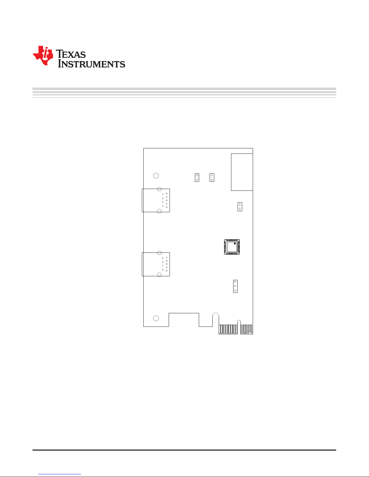
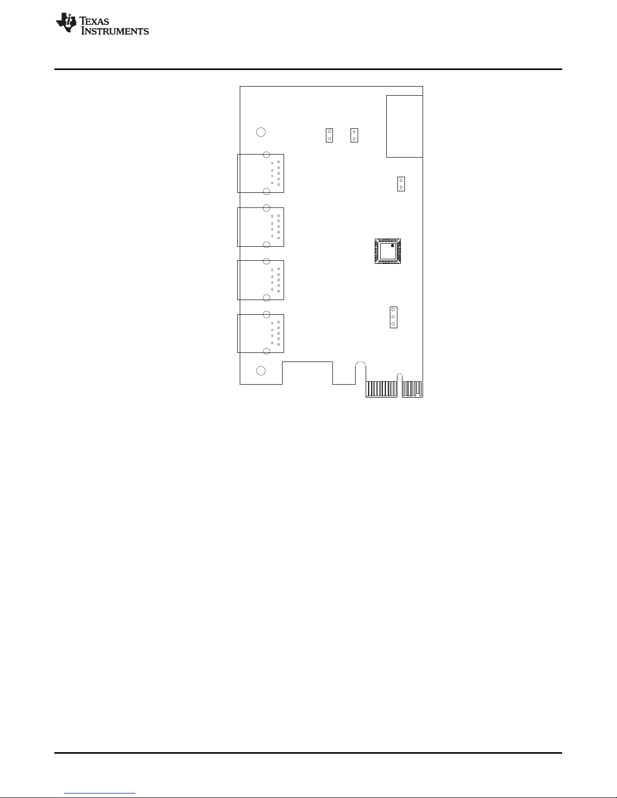
1 TUSB7320 and TUSB7340 DEMO Boards
The TUSB7320 and TUSB7340 DEMO boards are both PCI Express X1 Standard Height cards. The
dimensions of both boards are 4.376 inches by 2.571 inches. The two figures below depict how the boards
look.
SLLU146C–May 2011–Revised May 2014
EVM Board
6
EVM Board SLLU146C–May 2011–Revised May 2014
Figure 1. TUSB7320 DEMO EVM REVB
Copyright © 2011–2014, Texas Instruments Incorporated
Submit Documentation Feedback
Page 7
J1
J5
PORT3
PORT1
PORT2
PORT4
J2
J3
J4
U1
J26J27
J22
J40
www.ti.com
TUSB7320 and TUSB7340 DEMO Boards
Figure 2. TUSB7340 DEMO EVM REVB
SLLU146C–May 2011–Revised May 2014 EVM Board
Submit Documentation Feedback
7
Copyright © 2011–2014, Texas Instruments Incorporated
Page 8
Hardware Setup
2 Hardware Setup
2.1 Headers
The EVM boards are populated with three headers: J22, J26, and J40.
J22 header is used to change the state of AUX_DET signal to the TUSB73XX. By default, this header is
not shorted and therefore AUX_DET will be high. If a jumper shunt is placed over J22, the AUX_DET will
be low.
The J26 header is used to route 5 V from the IDE Power Connector (J5) to the Texas Instruments
TPS2560 USB power switch. This header should always have a Jumper Shunt populated. For more
information on the Texas Instruments TPS2560, please visit www.ti.com.
J40 header is used to select the 3.3-V power source for the TUSB73X0. By default, a Jumper Shunt
should be populated across pins 1 and 2 of J40. When in this position, the 3.3-V power from the PCI
Express slot is routed to the TUSB73X0. If the Jumper Shunt is moved to pins 2 and 3, then the 3.3-V
VAUX power from the PCI Express slot is routed to the TUSB73X0. The Jumper Shunt should only be
moved to positions 2 and 3 if wake testing is required. Otherwise the jumper should be left in the default
position of 1 and 2.
NOTE: The 3.3-V VAUX power supply has a limited current capability. According to the PCI Express
Electromechanical Spec, the 3.3-V VAUX will have a maximum current of 375 mA. Because
of the limited current of 3.3-V VAUX, it is recommended to plug only one device into the
TUSB73X0. If the Jumper Shunt is left on pins 1 and 2 of J40, this current limitation does not
exist and therefore all ports of the TUSB73X0 can be used.
www.ti.com
2.2 VBUS
VBUS for all of the USB ports comes from the IDE Power Connector (J5).
2.3 PCI Express Slot Options
Because the TUSB73X0 EVM boards are PCI Express X1, they can be used in any PCI Express Slot
(X1, X4, X8, or X16) on a typical motherboard. The boards can be used in either a PCI Express Gen1
(2.5 Gbps) or Gen2 (5 Gbps) slot. Because of the speed of USB3 (5 Gbps), if used in a PCI Express
Gen1 slot, the performance of the TUSB7320 or TUSB7340 will be negatively impacted. For this reason, it
is recommended to always insert the EVM board into a PCI Express Gen2 slot.
8
EVM Board SLLU146C–May 2011–Revised May 2014
Copyright © 2011–2014, Texas Instruments Incorporated
Submit Documentation Feedback
Page 9
SLLU146C–May 2011–Revised May 2014
Bringup
Below are the steps to bring up the EVM board in a typical system:
1. Remove the power plug from the PC power supply.
2. Make sure the Jumper Shunts are populated on J26 and J40.
3. Insert the EVM board into a PCI Express slot. It is recommended to use a PCI Express Gen2 slot if
one is available.
4. Insert an IDE Power Connector into J5 of the EVM board.
5. Insert the power plug into the PC power supply.
6. Turn the PC on. Once the PC is turned on, all of the green LEDs should be ON. If LED D5 is not
active, please check to make sure the jumper shunt on J40 is populated. If none of the green LEDs
(D1 thru D4) for each USB Port are active, please check to make sure the Jumper Shunt on J26 is
populated and an IDE Power connector is plugged into J5.
7. Once the PC has booted into Windows 7, you will need to install the TI xHCI driver. If the driver has
already been installed on your PC, then you can proceed step 8. Otherwise, you will need to install the
xHCI driver by running the TI xHCI driver setup utility.
8. You can now insert devices into the USB ports.
SLLU146C–May 2011–Revised May 2014 Bringup
Submit Documentation Feedback
9
Copyright © 2011–2014, Texas Instruments Incorporated
Page 10
SLLU146C–May 2011–Revised May 2014
WAKE Testing Setup
The EVM board can be used to test the WAKE functionality of the TUSB73X0. By default, the EVM is not
configured to support wake testing. Please configure the EVM according to the following if WAKE is
required:
1. Move the Jumper Shunt on J40 to pins 2 and 3.
2. Make sure there is no Jumper Shunt on J22.
3. Use a dedicated 5-V power supply for VBUS. Do NOT use the IDE Power connector provided from the
system power supply. The reason for not using the IDE power from system power supply is when the
system is put in a sleep or hibernate state, the power on the IDE Power connector will be turned off.
NOTE: For some motherboards, WAKE from a PCIe slot is not supported or is only supported on
PCIE X1 slots. Please make sure to use a motherboard that supports WAKE from any PCIe
slot.
10
WAKE Testing Setup SLLU146C–May 2011–Revised May 2014
Copyright © 2011–2014, Texas Instruments Incorporated
Submit Documentation Feedback
Page 11
SLLU146C–May 2011–Revised May 2014
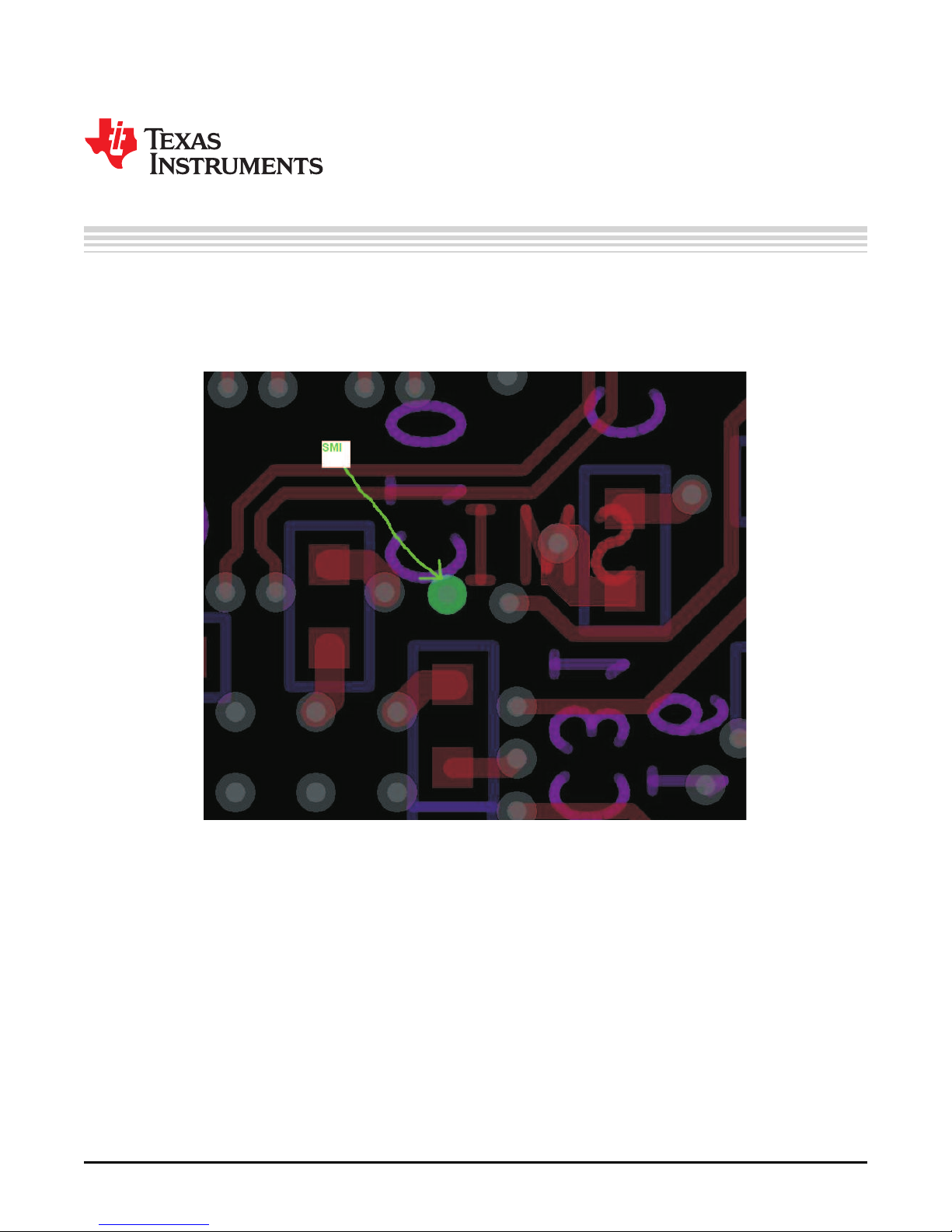
SMI Support
The SMI pin from the TUSB7320 is brought out to a header labeled SMI. This header is located to the left
of J22.
The SMI pin from the TUSB7340 is brought out to a via located on the bottom of board near U1. The via is
located between C10 and C34 and just above C31.
Figure 3. SMI via Location for TUSB7340 DEMO EVM REVB
SLLU146C–May 2011–Revised May 2014 SMI Support
Submit Documentation Feedback
11
Copyright © 2011–2014, Texas Instruments Incorporated
Page 12

SLLU146C–May 2011–Revised May 2014
The following pages contain schematics for the TUSB7320 and TUSB7340.
Schematics
12
Schematics SLLU146C–May 2011–Revised May 2014
Copyright © 2011–2014, Texas Instruments Incorporated
Submit Documentation Feedback
Page 13

EPROM
I2C
DP/DM
(U1)
TUSB7320
RX/TX USB3
TYPEA
PCIE
CONNECTOR
DOWNSTREAM
PORT1
DOWNSTREAM
PORT2
USB3
TYPEA
DP/DM
RX/TX
RX/TX
VIA AND TRACE REQUIREMENTS:
- MIN VIA PAD SIZE 20mils
- MIN spacing between trace and pad is 5mils
- MIN spacing between VIA and pad is 5mils
- MIN width of trace is 4mils
IMPEDANCE REQUIREMENTS:
- USB_DP/M must be 90-ohm differential (+/-15%)
- USB_SSTXP/N must be 90-ohms differential (+/-15%)
- USB_SSRXP/N must be 90-ohms differential (+/-15%)
- PCIE_TXP/N must be 100-ohms differential (+/-10%)
- PCIE_RXP/N must be 100-ohms differential (+/-10%)
- PCIE_REFCLKP/N must be 100-ohms differential (+/-10%)
LENGTH MATCHING REQUIREMENTS:
- USB_DP/M within 25mils.
- USB_SSTXP/N within 5mils
- USB_SSRXP/N within 5mils
- PCIE_TXP/N within 5mils
- PCIE_RXP/N within 5mils
- PCIE_REFCLKP/N within 25mils.
Sheet of
SIZE
SCAL E: NONE
DWG NO:
TUSB732 0 DEMO REVB _48
Friday, May 09, 2 014
B
1 4Sheet of
SIZE
SCAL E: NONE
DWG NO:
TUSB732 0 DEMO REVB _48
Friday, May 09, 2 014
B
1 4Sheet of
SIZE
SCAL E: NONE
DWG NO:
TUSB732 0 DEMO REVB _48
Friday, May 09, 2 014
B
1 4
www.ti.com
TUSB7320 DEMO EVM REVB Schematics
1 TUSB7320 DEMO EVM REVB Schematics
13
SLLU146C–May 2011– Revised May 2014 Schematics
Submit Documentation Feedback
Copyright © 2011–2014, Texas Instruments Incorporated
Page 14

POPULATE P ULLDOWN IF I2C EEPROM
NOT USED A ND DO NOT POPUL ATE
PULLUP.
PLACE CLOS E TO U1
JUMPER J22 FOR NO WAKE SUP PORT
POPULATE R 2 FOR WAKE SUPP ORT.
AUX_DET
SDA
R1EXT
R1EXTRTN
VSS_OSC
XO
XI
FREQSEL
SCL
GPIO0
GPIO1
GPIO2
GPIO3
VDDA3P3VBOARD_1P1V BOARD_3P3V
BOARD_3P3V
BOARD_3P3V
BOARD_3P3V
USB_DP_DN2 pg3
USB_DM_DN2 pg3
USB_SSTXP_DN2 pg3
USB_SSTXN_DN2 pg3
USB_SSRXP_DN2 pg3
USB_SSRXN_DN2 pg3
OVERCUR2Z pg3
PWRON2Z pg3
USB_DM_DN1 pg3
USB_DP_DN1 pg3
USB_SSRXN_DN1 pg3
USB_SSRXP_DN1 pg3
USB_SSTXN_DN1 pg3
USB_SSTXP_DN1 pg3
PWRON1Z pg3
OVERCUR1Z pg3
PCIE_REFCLKNpg3
PCIE_REFCLKPpg3
PCIE_RXNpg3
PCIE_RXPpg3
PCIE_TXNpg3
PCIE_TXPpg3
PERSTZpg3
WAKEZpg3
GRSTZpg4
Sheet of
SIZE
SCALE: NONE
DWG NO:
TUSB7320
Friday, May 09, 2014
C
2 4Sheet of
SIZE
SCALE: NONE
DWG NO:
TUSB7320
Friday, May 09, 2014
C
2 4Sheet of
SIZE
SCALE: NONE
DWG NO:
TUSB7320
Friday, May 09, 2014
C
2 4
J22
HDR2X1M .1
12
R3
NOPOP
0402
5%
C2
18pF
Y1
ECS-48MHZ
U2
24LC01_NF
A0
1
A1
2
A2
3
GND4SDA
5
SCL
6
WP
7
VCC
8
R11
4.7K
0402
5%
R1
NOPOP
0402
5%
R39
0
R2
10K
0402
5%
R38
0
C3
18pF
R12 1M
R10 9.09K 1 %
R4
NOPOP
0402
5%
C1
0.1uF
TUSB7320
TUSB7320_REVA
U1
CLKREQ#
B36
FREQSEL
B14
GPIO0
A49
GPIO1
B46
GPIO2
B47
GPIO3
B48
GRST#
A15
JTAG_RST#
B32
JTAG_TCK
A32
JTAG_TDI
A35
JTAG_TDO
B31
JTAG_TMS
B30
PCIE_REFCLKN
B41
PCIE_REFCLKP
A45
PCIE_RXN
A42
PCIE_RXP
B39
PCIE_TXN
A41
PCIE_TXP
B38
PERST#
A40
SCL
B2
SDA
A2
SMI
B3
WAKE#
B35
OVERCUR1#
A36
OVERCUR2#
A37
NC18
B43
NC26
B45
PWRON1#
B33
PWRON2#
B34
NC17
A46
NC25
A48
R1EXT
A24
R1EXTRTN
B23
USB_DM_DN1
B18
USB_DM_DN2
A13
NC11
A27
NC19
A5
USB_DP_DN1
A20
USB_DP_DN2
B12
NC12
B25
NC20
B5
USB_SSRXN_DN1
B16
USB_SSRXP_DN2
B9
NC13
A29
NC21
A7
USB_SSRXP_DN1
A18
USB_SSRXN_DN2
A10
NC14
B27
NC22
B6
USB_SSTXN_DN1
B15
USB_SSTXN_DN2
B10
NC15
A30
NC23
A8
USB_SSTXP_DN1
A17
USB_SSTXP_DN2
A11
NC16
B28
NC24
B7
VSS_OSC
B21
XI
A23
XO
A22
AUX_DET
A52
VDDA_3P3
A25
VDD11A1VDD11
A12
VDD11
A16
VDD11
A28
VDD11
A31
VDD11
A33
VDD11
A38
VDD11
A4
NC6
A43
VDD11
A50
VDD11A6VDD11A9VDD11B1VDD11
B17
VDD11
B19
VDD11
B24
VDD11
B37
VDD11
B40
VDD11
B42
VDD11
B44
VDD11
B8
VDD33A3VDD33
A34
VDD33
A39
VDD33
A47
VDD33
A51
VDDA_3P3
A19
VDDA_3P3
A21
VDDA_3P3
A44
VDDA_3P3
B11
VDDA_3P3
B22
NC28
B26
NC27
B4
NC1
A14
NC2
A26
NC3
B13
NC4
B29
VSS
B20
VSS
A53
NC7C1NC8C2NC9C3NC10
C4
BOARD_1P1V
C32
0.1uF
C17
0.1uF
C36
0.01uF
C12
0.01uF
C31
0.1uF
C18
0.01uF
C34
0.1uF
C20
0.1uF
C21
0.01uF
C23
0.1uF
C16
0.1uF
C37
0.1uF
C13
0.1uF
C30
0.01uF
C33
0.01uF
C24
22uF
C19
0.1uF
C35
0.1uF
C14
0.1uF
C22
0.1uF
C15
0.01uF
GPIO0
GPIO1
GPIO2
GPIO3
BOARD_3P3V
R7
NOPOP
0402
5%
R6
NOPOP
0402
5%
R8
NOPOP
0402
5%
R5
NOPOP
0402
5%
VDDA3P3V
BOARD_3P3V
C6
0.1uF
C28
0.1uF
FB1
220 @ 100MHZ
C25
0.1uF
C9
0.1uF
C7
0.01uF
C11
0.1uF
C29
0.1uF
C5
0.01uF
C26
0.1uF
C10
0.01uF
C4
22uF
C8
0.1uF
C27
0.1uF
TUSB7320 DEMO EVM REVB Schematics
www.ti.com
14
Schematics SLLU146C–May 2011–Revised May 2014
Submit Documentation Feedback
Copyright © 2011–2014, Texas Instruments Incorporated
Page 15

DOWNSTREAM
PORT1
DOWNSTREAM
PORT2
JUMPER BETWEEN 1 AND
2 FOR NORMAL
OPERATION.
JUMPER BETWEEN 2 AND
3 FOR WAKE TESTING.
PCIE CEM SPEC MAX VALUES:
PCIE_3P3V: 3 AMPS.
VAUX: 375mA
ILIM1
DS1_VBUS
DS2_VBUS
LEDDS1
LEDDS3
CAP_US_TXN
CAP_US_TXP
PCIE_PRSNTZ
PCIE_TDITDO
WAKEZ_R
USB_SSRXN_DN1
IND_USB_DP_DN1
DS1_VBUS
USB_SSRXP_DN1
IND_USB_DM_DN1
CAPDSTXP1
CAPDSTXN1
DS_SHLD
IND_DS_TXP1
IND_DS_TXN1
IND_DS_TXN2
CAPDSTXP2
CAPDSTXN2
IND_USB_DP_DN2
DS2_VBUS
USB_SSRXN_DN2
USB_SSRXP_DN2
IND_USB_DM_DN2
IND_DS_TXP2
DS_SHLDDS_SHLD
BOARD_5V
BOARD_3P3V
PCIE_3P3VPCIE_3P3V BOARD_12V
VAUX
BOARD_3P3V
PWRON2Zpg2
PWRON1Zpg2
PCIE_RXP pg2
PCIE_RXN pg2
PCIE_REFCLKN pg2
PCIE_REFCLKP p g2
WAKEZpg2
PERSTZ pg2
PCIE_TXN p g2
PCIE_TXP pg2
OVERCUR1Z pg2
OVERCUR2Z pg2
USB_DM_DN1 pg2
USB_SSRXN_DN1 pg2
USB_SSRXP_DN1 pg2
USB_DP_DN1 pg2
USB_SSTXP_DN1 pg2
USB_SSTXN_DN1 pg2
USB_SSTXP_DN2 pg2
USB_SSTXN_DN2 pg2
USB_DM_DN2 pg2
USB_DP_DN2 pg2
USB_SSRXN_DN2 pg2
USB_SSRXP_DN2 pg2
Sheet of
SIZE
SCALE: NONE
DWG NO:
USB3 AND PCIE CONNECTORS
Friday, May 09, 2014
C
3 4Sheet of
SIZE
SCALE: NONE
DWG NO:
USB3 AND PCIE CONNECTORS
Friday, May 09, 2014
C
3 4Sheet of
SIZE
SCALE: NONE
DWG NO:
USB3 AND PCIE CONNECTORS
Friday, May 09, 2014
C
3 4
R17
1M
0402
R13
10K
0402
5%
Side B
Component Side
SideA
Solder Side
Key
P1
PCIExpre ss x1 Edge Conne ctor
12V1
B1
12V2
B2
12V5
B3
GND1
B4
SMCLK
B5
SMDAT
B6
GND2
B7
3.3V
B8
J_TRST#
B9
3.3Vaux
B10
WAKE#
B11
RSVD2
B12
GND3
B13
PETp0
B14
PETn0
B15
GND4
B16
PRSNT2#
B17
GND5
B18
PRSNT1#
A1
12V3
A2
12V4
A3
GND9
A4
J_TCK
A5
J_TDI
A6
J_TDO
A7
J_TMS
A8
3.3V1
A9
3.3V2
A10
PERST#
A11
GND8
A12
REFCLK+
A13
REFCLK-
A14
GND7
A15
PERp0
A16
PERn0
A17
GND6
A18
J40
HDR1x3
1
2
3
R18
NOPOP
C62
NOPOP
R14
10K
0402
5%
U26
TPD2EUSB30_NF
D+
1
D-
2
GND
3
C79
1000pF
C48 0.1uF
R15
330
0402
5%
+
C80
NOPOP
+
C44
150uF
L4
TDK_TCE_121 0
1
2 3
4
R50 0
C41
0.1uF
C47 0.1uF
C43
0.1uF
R20
NOPOP
D1
LED Green 0 805
+
C46
150uF
C64
22uF
U3
TPS2560DRC
GND
1
IN
2
IN
3
EN1
4
EN2
5
FAULT2Z
6
ILIM
7
OUT2
8
OUT1
9
FAULT1Z
10
PAD
11
C67 0.1 uF
C45
0.1uF
C63
NOPOP
R19
30.9K
0402
1%
C42
0.001uF
C68 0.1 uF
L7
TDK_TCE_121 0
1
2 3
4
R16
330
0402
5%
J4
USB3_TYPEA_CONNECTER
VBUS
1
DM
2
DP
3
GND
4
SSRXN
5
SSRXP
6
GND
7
SSTXN
8
SSTXP
9
SHIELD0
10
SHIELD1
11
C49
0.1uF
C50
0.001uF
C40 0.1uF
D2
LED Green 0 805
L5
TDK_TCE_121 0
1
2 3
4
MH2
PLATED_MH
1
R21
1M
0402
C39 0.1uF
MH1
PLATED_MH
1
C38
0.1uF
U27
TPD2EUSB30_NF
D+
1
D-
2
GND
3
L2
TDK_TCE_121 0
1
2 3
4
J1
USB3_TYPEA_CONNECTER
VBUS
1
DM
2
DP
3
GND
4
SSRXN
5
SSRXP
6
GND
7
SSTXN
8
SSTXP
9
SHIELD0
10
SHIELD1
11
www.ti.com
TUSB7320 DEMO EVM REVB Schematics
15
SLLU146C–May 2011– Revised May 2014 Schematics
Submit Documentation Feedback
Copyright © 2011–2014, Texas Instruments Incorporated
Page 16

1.1V REGULATOR
5V VBUS OPTIONS
NOTE: USE LOW ESR CAP
NOTE: USE LOW ESR CAP
OPTION 1: 5V REGULATOR OPTION 2: 5V FROM IDE CONNECTOR
NOTE: ONLY POPULATE ONE OPTION
R33 R35 OUTPUT
1.13K 4.53K 1.0V
1.37K 4.42K 1.05V
1.87K 4.99K 1.1V (DEFAULT)
2.49K 4.99K 1.2V
EN1P1
SS1P1
FB_1P T1V
VSENSE
BOOT PH
LED3V
BOARD _1P1V
BOARD _3P3V
BOARD _3P3V
REG_5 V BOARD _12V
IDE_ 5V
IDE_ 5V
REG_5 V
BOARD _5V
GRSTZ pg2
Sheet of
SIZE
SCALE : NONE
DWG NO :
POW ER
Friday, May 09, 20 14
B
4 4Sheet of
SIZE
SCALE : NONE
DWG NO :
POW ER
Friday, May 09, 20 14
B
4 4Sheet of
SIZE
SCALE : NONE
DWG NO :
POW ER
Friday, May 09, 20 14
B
4 4
J27
NOPOP
1 2
L1
15uH_NF
R37
3.16K_ NF
1%
C78
0.01uF_ NF
D5
LED Gre en 0805
+5V
GND0
GND1
+12V
J5
IDE_ PWR_C ONN
4
3
2
1
+
C73
330uF_ NF
R36
10K_NF
1%
U5
TPS74 401RG WT
OUT
1
NC2NC3NC
4
IN
5
IN
6
IN
7
IN
8
PG
9
BIAS
10
EN
11
GND12NC13NC
14
SS
15
FB
16
NC
17
OUT
18
OUT
19
OUT
20
PAD
21
C69
10uF
R34
330
0402
5%
C85
0.1uF
C70
22uF
D6
MBRS54 0T3_NF
R32
4.7K
0402
5%
C75
0.01uF_ NF
C74
0.01uF_ NF
R31
10K
0402
5%
C71
0.01uF
R33
1.87K
0402
1%
C72
NOPOP
J26
HDR2X1 M .1
1 2
R35
4.99K
0402
1%
C76
22uF
C77
22uF_NF
U6
TPS54 50_NF
BOOT
1
NC
2
NC_
3
VSENSE4ENA
5
GND
6
VIN
7
PH
8
GND
9
TUSB7320 DEMO EVM REVB Schematics
www.ti.com
16
Schematics SLLU146C–May 2011–Revised May 2014
Submit Documentation Feedback
Copyright © 2011–2014, Texas Instruments Incorporated
Page 17

EPROM
I2C
DP/DM
(U1)
TUSB7340
RX/TX USB3
TYPEA
PCIE
CONNECTOR
DOWNSTREAM
PORT1
DOWNSTREAM
PORT2
USB3
TYPEA
USB3
TYPEA
USB3
TYPEA
DOWNSTREAM
PORT3
DOWNSTREAM
PORT4
DP/DM
RX/TX
DP/DM
RX/TX
DP/DM
RX/TX
RX/TX
VIA AND TRACE REQUIREMENTS:
- MIN VIA PAD SIZE 20mils
- MIN spacing between trace and pad is 5mils
- MIN spacing between VIA and pad is 5mils
- MIN width of trace is 4mils
IMPEDANCE REQUIREMENTS:
- USB_DP/M must be 90-ohm differential (+/-15%)
- USB_SSTXP/N must be 90-ohms differential (+/-15%)
- USB_SSRXP/N must be 90-ohms differential (+/-15%)
- PCIE_TXP/N must be 100-ohms differential (+/-10%)
- PCIE_RXP/N must be 100-ohms differential (+/-10%)
- PCIE_REFCLKP/N must be 100-ohms differential (+/-10%)
LENGTH MATCHING REQUIREMENTS:
- USB_DP/M within 25mils.
- USB_SSTXP/N within 5mils
- USB_SSRXP/N within 5mils
- PCIE_TXP/N within 5mils
- PCIE_RXP/N within 5mils
- PCIE_REFCLKP/N within 25mils.
Sheet of
SIZE
SCAL E: NONE
DWG NO:
TUSB734 0_DEMO_REV B_48
Friday, May 09, 2 014
B
1 4Sheet of
SIZE
SCAL E: NONE
DWG NO:
TUSB734 0_DEMO_REV B_48
Friday, May 09, 2 014
B
1 4Sheet of
SIZE
SCAL E: NONE
DWG NO:
TUSB734 0_DEMO_REV B_48
Friday, May 09, 2 014
B
1 4
www.ti.com
TUSB7340 DEMO EVM REVB Schematics
2 TUSB7340 DEMO EVM REVB Schematics
17
SLLU146C–May 2011– Revised May 2014 Schematics
Submit Documentation Feedback
Copyright © 2011–2014, Texas Instruments Incorporated
Page 18

POPULATE PULLDOW N IF I2C EEPROM
NOT USED AND DO NOT POP ULATE
PULLUP.
PLACE CLOS E TO U1
POPULATE R2 FOR WAKE SU PPORT. JUMPER J22 FOR N O WAKESUPPORT
AUX_DET
SDA
R1EXT
R1EXTRTN
VSS_OSC
XO
XI
FREQSEL
SCL
GPIO0
GPIO1
GPIO2
GPIO3
GPIO0
GPIO1
GPIO2
GPIO3
VDDA3P3VBOARD_1P1V BOARD_3P3V
BOARD_3P3V
BOARD_3P3V
BOARD_3P3V
BOARD_3P3V
USB_DP_DN2 pg3
USB_DM_DN2 pg3
USB_SSTXP_DN2 pg3
USB_SSTXN_DN2 pg3
USB_SSRXP_DN2 pg3
USB_SSRXN_DN2 pg3
OVERCUR2Z pg3
PWRON2Z pg3
USB_SSRXN_DN3 pg3
USB_DP_DN3 pg3
USB_DM_DN3 pg3
PWRON3Z pg3
USB_SSTXP_DN3 pg3
USB_SSTXN_DN3 pg3
USB_SSRXP_DN3 pg3
OVERCUR3Z pg3
USB_SSRXP_DN4 pg3
USB_SSRXN_DN4 pg3
USB_DP_DN4 pg3
USB_DM_DN4 pg3
OVERCUR4Z pg3
PWRON4Z pg3
USB_SSTXP_DN4 pg3
USB_SSTXN_DN4 pg3
USB_DM_DN1 pg3
USB_DP_DN1 pg3
USB_SSRXN_DN1 pg3
USB_SSRXP_DN1 pg3
USB_SSTXN_DN1 pg3
USB_SSTXP_DN1 pg3
PWRON1Z pg3
OVERCUR1Z pg3
PCIE_REFCLKNpg3
PCIE_REFCLKPpg3
PCIE_RXNpg3
PCIE_RXPpg3
PCIE_TXNpg3
PCIE_TXPpg3
PERSTZpg3
WAKEZpg3
GRSTZpg4
Sheet of
SIZE
SCALE: NONE
DWG NO:
TUSB7340
Friday, May 09, 2014
C
2 4Sheet of
SIZE
SCALE: NONE
DWG NO:
TUSB7340
Friday, May 09, 2014
C
2 4Sheet of
SIZE
SCALE: NONE
DWG NO:
TUSB7340
Friday, May 09, 2014
C
2 4
R3
NOPOP
0402
5%
C2
18pF
Y1
ECS-48MHZ
U2
24LC01_NF
A0
1
A1
2
A2
3
GND4SDA
5
SCL
6
WP
7
VCC
8
R11
4.7K
0402
5%
R7
NOPOP
0402
5%
R1
NOPOP
0402
5%
R39
0
R38
0
R6
NOPOP
0402
5%
R8
NOPOP
0402
5%
C3
18pF
R12 1M
R10 9 .09K 1%
R2
10K
0402
5%
J22
HDR2X1M . 1
12
R4
NOPOP
0402
5%
C1
0.1uF
TUSB7340
TUSB7340_REVA
U1
CLKREQ#
B36
FREQSEL
B14
GPIO0
A49
GPIO1
B46
GPIO2
B47
GPIO3
B48
GRST#
A15
JTAG_RST#
B32
JTAG_TCK
A32
JTAG_TDI
A35
JTAG_TDO
B31
JTAG_TMS
B30
PCIE_REFCLKN
B41
PCIE_REFCLKP
A45
PCIE_RXN
A42
PCIE_RXP
B39
PCIE_TXN
A41
PCIE_TXP
B38
PERST#
A40
SCL
B2
SDA
A2
SMI
B3
WAKE#
B35
OVERCUR1#
A36
OVERCUR2#
A37
OVERCUR3#
B43
OVERCUR4#
B45
PWRON1#
B33
PWRON2#
B34
PWRON3#
A46
PWRON4#
A48
R1EXT
A24
R1EXTRTN
B23
USB_DM_DN1
B18
USB_DM_DN2
A13
USB_DM_DN3
A27
USB_DM_DN4
A5
USB_DP_DN1
A20
USB_DP_DN2
B12
USB_DP_DN3
B25
USB_DP_DN4
B5
USB_SSRXN_DN1
B16
USB_SSRXP_DN2
B9
USB_SSRXN_DN3
A29
USB_SSRXN_DN4
A7
USB_SSRXP_DN1
A18
USB_SSRXN_DN2
A10
USB_SSRXP_DN3
B27
USB_SSRXP_DN4
B6
USB_SSTXN_DN1
B15
USB_SSTXN_DN2
B10
USB_SSTXN_DN3
A30
USB_SSTXN_DN4
A8
USB_SSTXP_DN1
A17
USB_SSTXP_DN2
A11
USB_SSTXP_DN3
B28
USB_SSTXP_DN4
B7
VSS_OSC
B21
XI
A23
XO
A22
AUX_DET
A52
VDDA_3P3
A25
VDD11A1VDD11
A12
VDD11
A16
VDD11
A28
VDD11
A31
VDD11
A33
VDD11
A38
VDD11
A4
NC6
A43
VDD11
A50
VDD11A6VDD11A9VDD11B1VDD11
B17
VDD11
B19
VDD11
B24
VDD11
B37
VDD11
B40
VDD11
B42
VDD11
B44
VDD11
B8
VDD33A3VDD33
A34
VDD33
A39
VDD33
A47
VDD33
A51
VDDA_3P3
A19
VDDA_3P3
A21
VDDA_3P3
A44
VDDA_3P3
B11
VDDA_3P3
B22
VDDA_3P3
B26
VDDA_3P3
B4
NC1
A14
NC2
A26
NC3
B13
NC4
B29
VSS
B20
VSS
A53
NC7C1NC8C2NC9C3NC10
C4
R5
NOPOP
0402
5%
BOARD_1P1V
C32
0.1uF
C17
0.1uF
C36
0.01uF
C12
0.01uF
C31
0.1uF
C18
0.01uF
C34
0.1uF
C20
0.1uF
C21
0.01uF
C23
0.1uF
C16
0.1uF
C37
0.1uF
C13
0.1uF
C30
0.01uF
C33
0.01uF
C24
22uF
C19
0.1uF
C35
0.1uF
C14
0.1uF
C22
0.1uF
C15
0.01uF
VDDA3P3V
BOARD_3P3V
C6
0.1uF
C28
0.1uF
FB1
220 @ 100MHZ
C25
0.1uF
C9
0.1uF
C7
0.01uF
C11
0.1uF
C29
0.1uF
C5
0.01uF
C26
0.1uF
C10
0.01uF
C4
22uF
C8
0.1uF
C27
0.1uF
TUSB7340 DEMO EVM REVB Schematics
www.ti.com
18
Schematics SLLU146C–May 2011–Revised May 2014
Submit Documentation Feedback
Copyright © 2011–2014, Texas Instruments Incorporated
Page 19

DOWNSTREAM
PORT1
DOWNSTREAM
PORT2
DOWNSTREAM
PORT3
DOWNSTREAM
PORT4
JUMPER BETWEEN 1 AND
2 FOR NORMAL
OPERATION.
JUMPER BETWEEN 2 AND
3 FOR WAKE TESTING.
PCIE CEM SPEC MAX VALUES:
PCIE_3P3V: 3 AMPS.
VAUX: 375mA
IND_USB_DP_DN1
DS1_VBUS
USB_SSRXP_DN1
IND_USB_DM_DN1
IND_USB_DP_DN2
DS2_VBUS
USB_SSRXN_DN2
USB_SSRXP_DN2
IND_USB_DM_DN2
ILIM1
DS3_VBUS
DS1_VBUS
DS_SHLD
LEDDS1
LEDDS3
CAP_US_TXN
CAP_US_TXP
PCIE_PRSNTZ
PCIE_TDITDO
ILIM2
DS2_VBUS
DS4_VBUS
LEDDS4
LEDDS2
IND_USB_DP_DN3
DS3_VBUS
USB_SSRXP_DN3
USB_SSRXN_DN3
IND_USB_DM_DN3
IND_USB_DP_DN4
DS4_VBUS
USB_SSRXN_DN4
USB_SSRXP_DN4
IND_USB_DM_DN4
DS_SHLDDS_SHLD
DS_SHLDDS_SHLD
DS_SHLDDS_SHLD
IND_DS_TXN1
IND_DS_TXP1
IND_DS_TXN2
IND_DS_TXP2
IND_DS_TXN3
IND_DS_TXP3
IND_DS_TXN4
IND_DS_TXP4
WAKEZ_R
USB_SSRXN_DN1
CAPDSTXP1
CAPDSTXN1
CAPDSTXP2
CAPDSTXN2
CAPDSTXP3
CAPDSTXN3
CAPDSTXP4
CAPDSTXN4
BOARD_5V
BOARD_3P3V
BOARD_5V
BOARD_3P3V
PCIE_3P3VPCIE_3P3V BOARD_12V
VAUX
BOARD_3P3V
PWRON1Zpg2
PWRON3Zpg2
PCIE_RXP p g2
PCIE_RXN pg 2
PCIE_REFCLKN pg2
PCIE_REFCLKP pg2
WAKEZpg2
PERSTZ pg2
PCIE_TXN pg2
PCIE_TXP pg2
PWRON4Zpg2
PWRON2Zpg2
OVERCUR3Z pg2
OVERCUR1Z pg2
OVERCUR2Z pg2
OVERCUR4Z pg2
USB_DM_DN1 pg2
USB_DP_DN1 pg2
USB_SSRXP_DN1 pg2
USB_SSRXN_DN1 pg2
USB_SSTXN_DN1 pg2
USB_SSTXP_DN1 pg2
USB_DM_DN2 pg2
USB_DP_DN2 pg2
USB_SSRXN_DN2 pg2
USB_SSRXP_DN2 p g2
USB_SSTXP_DN2 pg2
USB_SSTXN_DN2 pg2
USB_SSTXN_DN3 pg2
USB_SSTXP_DN3 pg2
USB_DM_DN3 pg2
USB_DP_DN3 pg2
USB_SSRXP_DN3 pg2
USB_SSRXN_DN3 pg 2
USB_SSTXP_DN4 pg2
USB_SSTXN_DN4 pg 2
USB_DM_DN4 pg2
USB_DP_DN4 pg2
USB_SSRXN_DN4 pg2
USB_SSRXP_DN4 pg2
Sheet of
SIZE
SCALE: NONE
DWG NO:
USB3 AND PCIE CONNECTORS
Friday, May 09, 2014
C
3 4Sheet of
SIZE
SCALE: NONE
DWG NO:
USB3 AND PCIE CONNECTORS
Friday, May 09, 2014
C
3 4Sheet of
SIZE
SCALE: NONE
DWG NO:
USB3 AND PCIE CONNECTORS
Friday, May 09, 2014
C
3 4
C41
0.1uF
C39 0.1uF
R30
1M
0402
L5
TDK_TCE_1210
1
2 3
4
R13
10K
0402
5%
Side B
Component Side
SideA
Solder Side
Key
P1
PCIExpres s x1 Edge Conne ctor
12V1
B1
12V2
B2
12V5
B3
GND1
B4
SMCLK
B5
SMDAT
B6
GND2
B7
3.3V
B8
J_TRST#
B9
3.3Vaux
B10
WAKE#
B11
RSVD2
B12
GND3
B13
PETp0
B14
PETn0
B15
GND4
B16
PRSNT2#
B17
GND5
B18
PRSNT1#
A1
12V3
A2
12V4
A3
GND9
A4
J_TCK
A5
J_TDI
A6
J_TDO
A7
J_TMS
A8
3.3V1
A9
3.3V2
A10
PERST#
A11
GND8
A12
REFCLK+
A13
REFCLK-
A14
GND7
A15
PERp0
A16
PERn0
A17
GND6
A18
L2
TDK_TCE_1210
1
2 3
4
C62
NOPOP
R14
10K
0402
5%
C49
0.1uF
L4
TDK_TCE_1210
1
2 3
4
R24
330
0402
5%
U26
TPD2EUSB30_NF
D+
1
D-
2
GND
3
C51
0.1uF
C56 0.1uF
C50
0.001uF
C42
0.001uF
R15
330
0402
5%
D3
LED Green 08 05
R21
1M
0402
+
C44
150uF
L10
TDK_TCE_1210
1
2 3
4
U27
TPD2EUSB30_NF
D+
1
D-
2
GND
3
C79
1000pF
R50 0
R23
10K
0402
5%
C43
0.1uF
+
C80
NOPOP
D1
LED Green 08 05
+
C46
150uF
C64
22uF
U3
TPS2560DRC
GND
1
IN
2
IN
3
EN1
4
EN2
5
FAULT2Z
6
ILIM
7
OUT2
8
OUT1
9
FAULT1Z
10
PAD
11
R22
10K
0402
5%
C67 0.1uF
C45
0.1uF
+
C55
150uF
C63
NOPOP
L8
TDK_TCE_1210
1
2 3
4
C60 0.1uF
R19
30.9K
0402
1%
C68 0.1uF
R16
330
0402
5%
J2
USB3_TYPEA_CONNECTER
VBUS
1
DM
2
DP
3
GND
4
SSRXN
5
SSRXP
6
GND
7
SSTXN
8
SSTXP
9
SHIELD0
10
SHIELD1
11
C48 0.1uF
C54
0.1uF
R29
1M
0402
+
C53
150uF
U24
TPD2EUSB30_NF
D+
1
D-
2
GND
3
D2
LED Green 08 05
C61 0.1uF
MH2
PLATED_MH
1
C58
0.1uF
J40
HDR1x3
1
2
3
R25
330
0402
5%
J4
USB3_TYPEA_CONNECTER
VBUS
1
DM
2
DP
3
GND
4
SSRXN
5
SSRXP
6
GND
7
SSTXN
8
SSTXP
9
SHIELD0
10
SHIELD1
11
L13
TDK_TCE_1210
1
2 3
4
C52
0.1uF
C59
0.001uF
U4
TPS2560DRC
GND
1
IN
2
IN
3
EN1
4
EN2
5
FAULT2Z
6
ILIM
7
OUT2
8
OUT1
9
FAULT1Z
10
PAD
11
MH1
PLATED_MH
1
C38
0.1uF
R27
30.9K
0402
1%
C40 0.1uF
D4
LED Green 08 05
C65
0.1uF
L7
TDK_TCE_1210
1
2 3
4
U25
TPD2EUSB30_NF
D+
1
D-
2
GND
3
C47 0.1uF
L11
TDK_TCE_1210
1
2 3
4
C66
0.001uF
C57 0.1uF
J1
USB3_TYPEA_CONNECTER
VBUS
1
DM
2
DP
3
GND
4
SSRXN
5
SSRXP
6
GND
7
SSTXN
8
SSTXP
9
SHIELD0
10
SHIELD1
11
J3
USB3_TYPEA_CONNECTER
VBUS
1
DM
2
DP
3
GND
4
SSRXN
5
SSRXP
6
GND
7
SSTXN
8
SSTXP
9
SHIELD0
10
SHIELD1
11
R17
1M
0402
www.ti.com
TUSB7340 DEMO EVM REVB Schematics
19
SLLU146C–May 2011– Revised May 2014 Schematics
Submit Documentation Feedback
Copyright © 2011–2014, Texas Instruments Incorporated
Page 20
1.1V REGULATOR
5V VBUS OPTIONS
R33 R35 OUTPUT
1.13K 4.53K 1.0V
1.37K 4.42K 1.05V
1.87K 4.99K 1.1V (DEFAULT)
2.49K 4.99K 1.2V
EN1P1
SS1P1
FB_1P T1V
LED3V
BOARD _1P1V
BOARD _3P3V
BOARD _3P3V
GRSTZ pg2
D5
LED Gre en 0805
U5
TPS74 401RG WT
OUT
1
NC2NC3NC
4
IN
5
IN
6
IN
7
IN
8
PG
9
BIAS
10
EN
11
GND12NC13NC
14
SS
15
FB
16
NC
17
OUT
18
OUT
19
OUT
20
PAD
21
C69
10uF
C85
0.1uF
R34
330
0402
5%
C70
22uF
R32
4.7K
0402
5%
R31
10K
0402
5%
C71
0.01uF
R33
1.87K
0402
1%
C72
NOPOP
R35
4.99K
0402
1%
NOTE: USE LOW ESR CAP
NOTE: USE LOW ESR CAP
OPTION 1: 5V REGULATOR OPTION 2: 5V FROM IDE CONNECTOR
NOTE: ONLY POPULATE ONE OPTION
VSENSE
BOOT PH
REG_5 V BOARD _12V
IDE_ 5V
IDE_ 5V
REG_5 V
BOARD _5V
Sheet of
SIZE
SCALE : NONE
DWG NO :
POW ER
Friday, May 09, 20 14
B
4 4Sheet of
SIZE
SCALE : NONE
DWG NO :
POW ER
Friday, May 09, 20 14
B
4 4Sheet of
SIZE
SCALE : NONE
DWG NO :
POW ER
Friday, May 09, 20 14
B
4 4
J27
NOPOP
1 2
L1
15uH_NF
R37
3.16K_ NF
1%
C78
0.01uF_ NF
+5V
GND0
GND1
+12V
J5
IDE_ PWR_C ONN
4
3
2
1
+
C73
330uF_ NF
R36
10K_NF
1%
D6
MBRS54 0T3_NF
C75
0.01uF_ NF
C74
0.01uF_ NF
J26
HDR2X1 M .1
1 2
C77
22uF_NF
C76
22uF
U6
TPS54 50_NF
BOOT
1
NC
2
NC_
3
VSENSE4ENA
5
GND
6
VIN
7
PH
8
GND
9
TUSB7340 DEMO EVM REVB Schematics
www.ti.com
20
Schematics SLLU146C–May 2011–Revised May 2014
Submit Documentation Feedback
Copyright © 2011–2014, Texas Instruments Incorporated
Page 21

www.ti.com
Appendix A Bill of Materials
The below table is the bill of materials for the TUSB7320 DEMO EVM REVB board. The rows marked in
yellow are components that are not populated on the EVM board.
Table 1. TUSB7320 DEMO REVB BOM
Item Quantity Reference Part Footprint Tolerance Manufacturer Manufacturer PN
C1,C6,C8,C9,C11,C13,
C14,C16,C17,C19,C20,
1 35 C28,C29,C31,C32,C34, 0.1µF 402
2 2 C2,C3 18pF 402
3 3 C4,C24,C70 22µF 805
4 11 C18,C21,C30,C33,C36, 0.01µF 402
5 2 C42,C50 0.001µF 402
6 2 C44,C46 150µF CASE_D Panasonic EEEFP1A151AP
7 1 C62 NOPOP 1210
8 1 C63 NOPOP 805
9 2 C64,C76 22µF 1210
10 1 C69 10µF 805
11 1 C72 NOPOP 402
12 1 C73 330µF_NF THCAP_2P5MM Panasonic ECA-1CM331
13 3 C74,C75,C78 0.01µF_NF 402
14 1 C77 22µF_NF 1210
15 1 C79 1000pF 402
16 1 C80 NOPOP 7343
17 3 D1,D2,D5 LED Green 0805 805 Lumex SML-LX0805GC-TR
18 1 D6 MBRS540T3_NF DIODE_SMC On Semiconductor MBRS540T3G
19 1 FB1 220 @ 100MHZ 603 MuRata BLM18EG221SN1D
20 2 J1,J4 USB3_TYPEA USB3_TYPEA MainSuper AK2SA009K1
21 1 J5 IDE_PWR_CONN IDEPWR Molex 15-24-4441
22 2 J22,J26 HDR2X1 M .1 HDR_2X1
23 1 J27 NOPOP HDR_2X1
24 1 J40 HDR1x3 berg1x3
25 1 L1 15µH_NF DR127 Coiltronics DR127-150-R
26 4 L2,L4,L5,L7 TDK_TCE_1210 TDK_TCE_1210 TDK
27 2 MH1,MH2 PLATED_MH MH_125mil
28 1 P1 PCIe x1 Edge PCIe_X1
29 10 NOPOP 402 5%
30 4 R2,R13,R14,R31 10K 402 5%
31 1 R10 9.09K 402 1%
32 2 R11,R32 4.7K 402 5%
33 3 R12,R17,R21 1M 402 5%
34 3 R15,R16,R34 330 402 5%
35 1 R19 30.9K 402 1%
36 1 R33 1.87K 402 1%
37 1 R35 4.99K 402 1%
38 1 R36 10K_NF 402 1%
39 1 R37 3.16K_NF 402 1%
C22,C23,C25,C26,C27,
C35,C37,C38,C39,C40,
C41,C43,C45,C47,C48,
C49,C67,C68,C85
C5,C7,C10,C12,C15,
C71
TCE_1210_900_
2P_T
R1,R3,R4,R5,R6,R7,
R8,R9, R18,R20
SLLU146C–May 2011–Revised May 2014 Bill of Materials
Submit Documentation Feedback
21
Copyright © 2011–2014, Texas Instruments Incorporated
Page 22

Appendix A
www.ti.com
Table 1. TUSB7320 DEMO REVB BOM (continued)
Item Quantity Reference Part Footprint Tolerance Manufacturer Manufacturer PN
40 3 R38,R39,R50 0 402 5%
41 1 U1 TUSB7320QFN 100_QFN TI TUSB7320QFN
42 1 U2 24LC01_NF 8_SOIC MicroChip Tech 24LC01BT-I/SN
43 1 U3 TPS2560DRC 10_DRC TI TPS2560DRC
44 1 U5 TPS74401RGWT 20_RGW TI TPS74401RGWT
45 1 U6 TPS5450_NF DDA TI TPS5450DDAR
46 2 U26,U27 TPD2EUSB30 DRT_sot23 TI TPD2EUSB30DRT
47 1 Y1 ECS-48MHZ ECX-53B Abracon
48 2 Digikey H342-ND
49 1 PCI Bracket & Manufacturing ME-440-2AT-BB
50 1 J26,J40 Jump Shunt Tyco 881545-2
4-40x1/4 Machine Screw
Phillips
General Stamping
Corp.
ABM3B-48.000MHZ-
B2-T
The below table is the bill of materials for the TUSB7340 DEMO EVM REVB board. The rows marked in
yellow are components that are not populated on the EVM board.
Table 2. TUSB7340 DEMO REVB BOM
Item Quantity Reference Part Footprint Tolerance Manufacturer Manufacturer PN
C1,C6,C8,C9,C11,C13,
C14,C16,C17,C19,C20,
C22,C23,C25,C26,C27,
1 44 C35,C37,C38,C39,C40, 0.1µF 402
2 2 C2,C3 18pF 402
3 3 C4,C24,C70 22µF 805
4 11 C18,C21,C30,C33,C36, 0.01µF 402
5 4 C42,C50,C59,C66 0.001µF 402
6 4 C44,C46,C53,C55 150µF CASE_D Panasonic EEEFP1A151AP
7 1 C62 NOPOP 1210
8 1 C63 NOPOP 805
9 2 C64,C76 22µF 1210
10 1 C69 10µF 805
11 1 C72 NOPOP 402
12 1 C73 330µF_NF THCAP_2P5MM Panasonic ECA-1CM331
13 3 C74,C75,C78 0.01µF_NF 402
14 1 C77 22µF_NF 1210
15 1 C79 1000pF 402
16 1 C80 NOPOP 7343 XX XX
17 5 D1,D2,D3,D4,D5 LED Green 0805 805 Lumex SML-LX0805GC-TR
18 1 D6 MBRS540T3_NF DIODE_SMC On Semiconductor MBRS540T3G
19 1 FB1 220 @ 100MHZ 603 MuRata BLM18EG221SN1D
20 4 J1,J2,J3,J4 USB3_TYPEA USB3_TYPEA MainSuper AK2SA009K1
21 1 J5 IDE_PWR_CONN IDEPWR Molex 15-24-4441
22 2 J22,J26 HDR2X1 M .1 HDR_2X1
23 1 J27 NOPOP HDR_2X1
24 1 J40 HDR1x3 berg1x3
C28,C29,C31,C32,C34,
C41,C43,C45,C47,C48,
C49,C51,C52,C54,C56,
C57,C58,C60,C61,C65,
C67,C68, C85
C5,C7,C10,C12,C15,
C71
22
Bill of Materials SLLU146C–May 2011–Revised May 2014
Copyright © 2011–2014, Texas Instruments Incorporated
Submit Documentation Feedback
Page 23

www.ti.com
Revision History
Table 2. TUSB7340 DEMO REVB BOM (continued)
Item Quantity Reference Part Footprint Tolerance Manufacturer Manufacturer PN
25 1 L1 15µH_NF DR127 Coiltronics DR127-150-R
26 8 TDK_TCE_1210 TDK_TCE_1210 TDK
27 2 MH1,MH2 PLATED_MH MH_125mil
28 1 P1 PCI Express x1 Edge PCIe_X1
29 8 NOPOP 402 5%
30 6 10K 402 5%
31 1 R10 9.09K 402 1%
32 2 R11,R32 4.7K 402 5%
33 5 R12,R17,R21,R29,R30 1M 402 5%
34 5 R15,R16,R24,R25,R34 330 402 5%
35 2 R19,R27 30.9K 402 1%
36 1 R33 1.87K 402 1%
37 1 R35 4.99K 402 1%
38 1 R36 10K_NF 402 1%
39 1 R37 3.16K_NF 402 1%
40 3 R38,R39,R50 0 402 5%
41 1 U1 TUSB7340QFN 100_QFN TI TUSB7340QFN
42 1 U2 24LC01_NF 8_SOIC MicroChip Tech 24LC01BT-I/SN
43 2 U3,U4 TPS2560DRC 10_DRC TI TPS2560DRC
44 1 U5 TPS74401RGWT 20_RGW TI TPS74401RGWT
45 1 U6 TPS5450_NF DDA TI TPS5450DDAR
46 4 U24,U25,U26,U27 TPD2EUSB30 DRT_sot23 TI TPD2EUSB30DRT
47 1 Y1 ECS-48MHZ ECX-53B Abracon
48 2 Digikey H342-ND
49 1 PCI Bracket ME-440-2AT-BB
50 2 J26,J40 Jump Shunt Tyco 881545-2
L2,L4,L5,L7,L8,L10, TCE_1210_900_
L11, L13 2P_T
R1,R3,R4,R5,R6,R7,
R8,R9
R2,R13,R14,R22,R23,
R31
ABM3B-
48.000MHZ-B2-T
4-40x1/4 Machine Screw
Phillips
General Stamping &
Manufacturing Corp.
Changes from B Revision (August 2012) to C Revision ................................................................................................ Page
• Changed entire contents of Chapter 6: Schematics with Rev. B_48 ............................................................. 12
SLLU146C–May 2011–Revised May 2014 Revision History
Submit Documentation Feedback
Revision History
23
Copyright © 2011–2014, Texas Instruments Incorporated
Page 24

ADDITIONAL TERMS AND CONDITIONS, WARNINGS, RESTRICTIONS, AND DISCLAIMERS FOR
EVALUATION MODULES
Texas Instruments Incorporated (TI) markets, sells, and loans all evaluation boards, kits, and/or modules (EVMs) pursuant to, and user
expressly acknowledges, represents, and agrees, and takes sole responsibility and risk with respect to, the following:
1. User agrees and acknowledges that EVMs are intended to be handled and used for feasibility evaluation only in laboratory and/or
development environments. Notwithstanding the foregoing, in certain instances, TI makes certain EVMs available to users that do not
handle and use EVMs solely for feasibility evaluation only in laboratory and/or development environments, but may use EVMs in a
hobbyist environment. All EVMs made available to hobbyist users are FCC certified, as applicable. Hobbyist users acknowledge, agree,
and shall comply with all applicable terms, conditions, warnings, and restrictions in this document and are subject to the disclaimer and
indemnity provisions included in this document.
2. Unless otherwise indicated, EVMs are not finished products and not intended for consumer use. EVMs are intended solely for use by
technically qualified electronics experts who are familiar with the dangers and application risks associated with handling electrical
mechanical components, systems, and subsystems.
3. User agrees that EVMs shall not be used as, or incorporated into, all or any part of a finished product.
4. User agrees and acknowledges that certain EVMs may not be designed or manufactured by TI.
5. User must read the user's guide and all other documentation accompanying EVMs, including without limitation any warning or
restriction notices, prior to handling and/or using EVMs. Such notices contain important safety information related to, for example,
temperatures and voltages. For additional information on TI's environmental and/or safety programs, please visit www.ti.com/esh or
contact TI.
6. User assumes all responsibility, obligation, and any corresponding liability for proper and safe handling and use of EVMs.
7. Should any EVM not meet the specifications indicated in the user’s guide or other documentation accompanying such EVM, the EVM
may be returned to TI within 30 days from the date of delivery for a full refund. THE FOREGOING LIMITED WARRANTY IS THE
EXCLUSIVE WARRANTY MADE BY TI TO USER AND IS IN LIEU OF ALL OTHER WARRANTIES, EXPRESSED, IMPLIED, OR
STATUTORY, INCLUDING ANY WARRANTY OF MERCHANTABILITY OR FITNESS FOR ANY PARTICULAR PURPOSE. TI SHALL
NOT BE LIABLE TO USER FOR ANY INDIRECT, SPECIAL, INCIDENTAL, OR CONSEQUENTIAL DAMAGES RELATED TO THE
HANDLING OR USE OF ANY EVM.
8. No license is granted under any patent right or other intellectual property right of TI covering or relating to any machine, process, or
combination in which EVMs might be or are used. TI currently deals with a variety of customers, and therefore TI’s arrangement with
the user is not exclusive. TI assumes no liability for applications assistance, customer product design, software performance, or
infringement of patents or services with respect to the handling or use of EVMs.
9. User assumes sole responsibility to determine whether EVMs may be subject to any applicable federal, state, or local laws and
regulatory requirements (including but not limited to U.S. Food and Drug Administration regulations, if applicable) related to its handling
and use of EVMs and, if applicable, compliance in all respects with such laws and regulations.
10. User has sole responsibility to ensure the safety of any activities to be conducted by it and its employees, affiliates, contractors or
designees, with respect to handling and using EVMs. Further, user is responsible to ensure that any interfaces (electronic and/or
mechanical) between EVMs and any human body are designed with suitable isolation and means to safely limit accessible leakage
currents to minimize the risk of electrical shock hazard.
11. User shall employ reasonable safeguards to ensure that user’s use of EVMs will not result in any property damage, injury or death,
even if EVMs should fail to perform as described or expected.
12. User shall be solely responsible for proper disposal and recycling of EVMs consistent with all applicable federal, state, and local
requirements.
Certain Instructions. User shall operate EVMs within TI’s recommended specifications and environmental considerations per the user’s
guide, accompanying documentation, and any other applicable requirements. Exceeding the specified ratings (including but not limited to
input and output voltage, current, power, and environmental ranges) for EVMs may cause property damage, personal injury or death. If
there are questions concerning these ratings, user should contact a TI field representative prior to connecting interface electronics including
input power and intended loads. Any loads applied outside of the specified output range may result in unintended and/or inaccurate
operation and/or possible permanent damage to the EVM and/or interface electronics. Please consult the applicable EVM user's guide prior
to connecting any load to the EVM output. If there is uncertainty as to the load specification, please contact a TI field representative. During
normal operation, some circuit components may have case temperatures greater than 60°C as long as the input and output are maintained
at a normal ambient operating temperature. These components include but are not limited to linear regulators, switching transistors, pass
transistors, and current sense resistors which can be identified using EVMs’ schematics located in the applicable EVM user's guide. When
placing measurement probes near EVMs during normal operation, please be aware that EVMs may become very warm. As with all
electronic evaluation tools, only qualified personnel knowledgeable in electronic measurement and diagnostics normally found in
development environments should use EVMs.
Agreement to Defend, Indemnify and Hold Harmless. User agrees to defend, indemnify, and hold TI, its directors, officers, employees,
agents, representatives, affiliates, licensors and their representatives harmless from and against any and all claims, damages, losses,
expenses, costs and liabilities (collectively, "Claims") arising out of, or in connection with, any handling and/or use of EVMs. User’s
indemnity shall apply whether Claims arise under law of tort or contract or any other legal theory, and even if EVMs fail to perform as
described or expected.
Safety-Critical or Life-Critical Applications. If user intends to use EVMs in evaluations of safety critical applications (such as life support),
and a failure of a TI product considered for purchase by user for use in user’s product would reasonably be expected to cause severe
personal injury or death such as devices which are classified as FDA Class III or similar classification, then user must specifically notify TI
of such intent and enter into a separate Assurance and Indemnity Agreement.
Page 25

RADIO FREQUENCY REGULATORY COMPLIANCE INFORMATION FOR EVALUATION MODULES
Texas Instruments Incorporated (TI) evaluation boards, kits, and/or modules (EVMs) and/or accompanying hardware that is marketed, sold,
or loaned to users may or may not be subject to radio frequency regulations in specific countries.
General Statement for EVMs Not Including a Radio
For EVMs not including a radio and not subject to the U.S. Federal Communications Commission (FCC) or Industry Canada (IC)
regulations, TI intends EVMs to be used only for engineering development, demonstration, or evaluation purposes. EVMs are not finished
products typically fit for general consumer use. EVMs may nonetheless generate, use, or radiate radio frequency energy, but have not been
tested for compliance with the limits of computing devices pursuant to part 15 of FCC or the ICES-003 rules. Operation of such EVMs may
cause interference with radio communications, in which case the user at his own expense will be required to take whatever measures may
be required to correct this interference.
General Statement for EVMs including a radio
User Power/Frequency Use Obligations: For EVMs including a radio, the radio included in such EVMs is intended for development and/or
professional use only in legally allocated frequency and power limits. Any use of radio frequencies and/or power availability in such EVMs
and their development application(s) must comply with local laws governing radio spectrum allocation and power limits for such EVMs. It is
the user’s sole responsibility to only operate this radio in legally acceptable frequency space and within legally mandated power limitations.
Any exceptions to this are strictly prohibited and unauthorized by TI unless user has obtained appropriate experimental and/or development
licenses from local regulatory authorities, which is the sole responsibility of the user, including its acceptable authorization.
U.S. Federal Communications Commission Compliance
For EVMs Annotated as FCC – FEDERAL COMMUNICATIONS COMMISSION Part 15 Compliant
Caution
This device complies with part 15 of the FCC Rules. Operation is subject to the following two conditions: (1) This device may not cause
harmful interference, and (2) this device must accept any interference received, including interference that may cause undesired operation.
Changes or modifications could void the user's authority to operate the equipment.
FCC Interference Statement for Class A EVM devices
This equipment has been tested and found to comply with the limits for a Class A digital device, pursuant to part 15 of the FCC Rules.
These limits are designed to provide reasonable protection against harmful interference when the equipment is operated in a commercial
environment. This equipment generates, uses, and can radiate radio frequency energy and, if not installed and used in accordance with the
instruction manual, may cause harmful interference to radio communications. Operation of this equipment in a residential area is likely to
cause harmful interference in which case the user will be required to correct the interference at its own expense.
FCC Interference Statement for Class B EVM devices
This equipment has been tested and found to comply with the limits for a Class B digital device, pursuant to part 15 of the FCC Rules.
These limits are designed to provide reasonable protection against harmful interference in a residential installation. This equipment
generates, uses and can radiate radio frequency energy and, if not installed and used in accordance with the instructions, may cause
harmful interference to radio communications. However, there is no guarantee that interference will not occur in a particular installation. If
this equipment does cause harmful interference to radio or television reception, which can be determined by turning the equipment off and
on, the user is encouraged to try to correct the interference by one or more of the following measures:
• Reorient or relocate the receiving antenna.
• Increase the separation between the equipment and receiver.
• Connect the equipment into an outlet on a circuit different from that to which the receiver is connected.
• Consult the dealer or an experienced radio/TV technician for help.
Industry Canada Compliance (English)
For EVMs Annotated as IC – INDUSTRY CANADA Compliant:
This Class A or B digital apparatus complies with Canadian ICES-003.
Changes or modifications not expressly approved by the party responsible for compliance could void the user’s authority to operate the
equipment.
Concerning EVMs Including Radio Transmitters
This device complies with Industry Canada licence-exempt RSS standard(s). Operation is subject to the following two conditions: (1) this
device may not cause interference, and (2) this device must accept any interference, including interference that may cause undesired
operation of the device.
Concerning EVMs Including Detachable Antennas
Under Industry Canada regulations, this radio transmitter may only operate using an antenna of a type and maximum (or lesser) gain
approved for the transmitter by Industry Canada. To reduce potential radio interference to other users, the antenna type and its gain should
be so chosen that the equivalent isotropically radiated power (e.i.r.p.) is not more than that necessary for successful communication.
This radio transmitter has been approved by Industry Canada to operate with the antenna types listed in the user guide with the maximum
permissible gain and required antenna impedance for each antenna type indicated. Antenna types not included in this list, having a gain
greater than the maximum gain indicated for that type, are strictly prohibited for use with this device.
Page 26

Canada Industry Canada Compliance (French)
Cet appareil numérique de la classe A ou B est conforme à la norme NMB-003 du Canada
Les changements ou les modifications pas expressément approuvés par la partie responsable de la conformité ont pu vider l’autorité de
l'utilisateur pour actionner l'équipement.
Concernant les EVMs avec appareils radio
Le présent appareil est conforme aux CNR d'Industrie Canada applicables aux appareils radio exempts de licence. L'exploitation est
autorisée aux deux conditions suivantes : (1) l'appareil ne doit pas produire de brouillage, et (2) l'utilisateur de l'appareil doit accepter tout
brouillage radioélectrique subi, même si le brouillage est susceptible d'en compromettre le fonctionnement.
Concernant les EVMs avec antennes détachables
Conformément à la réglementation d'Industrie Canada, le présent émetteur radio peut fonctionner avec une antenne d'un type et d'un gain
maximal (ou inférieur) approuvé pour l'émetteur par Industrie Canada. Dans le but de réduire les risques de brouillage radioélectrique à
l'intention des autres utilisateurs, il faut choisir le type d'antenne et son gain de sorte que la puissance isotrope rayonnée équivalente
(p.i.r.e.) ne dépasse pas l'intensité nécessaire à l'établissement d'une communication satisfaisante.
Le présent émetteur radio a été approuvé par Industrie Canada pour fonctionner avec les types d'antenne énumérés dans le manuel
d’usage et ayant un gain admissible maximal et l'impédance requise pour chaque type d'antenne. Les types d'antenne non inclus dans
cette liste, ou dont le gain est supérieur au gain maximal indiqué, sont strictement interdits pour l'exploitation de l'émetteur.
Mailing Address: Texas Instruments, Post Office Box 655303, Dallas, Texas 75265
Copyright © 2014, Texas Instruments Incorporated
spacer
Important Notice for Users of EVMs Considered “Radio Frequency Products” in Japan
EVMs entering Japan are NOT certified by TI as conforming to Technical Regulations of Radio Law of Japan.
If user uses EVMs in Japan, user is required by Radio Law of Japan to follow the instructions below with respect to EVMs:
1. Use EVMs in a shielded room or any other test facility as defined in the notification #173 issued by Ministry of Internal Affairs and
Communications on March 28, 2006, based on Sub-section 1.1 of Article 6 of the Ministry’s Rule for Enforcement of Radio Law of
Japan,
2. Use EVMs only after user obtains the license of Test Radio Station as provided in Radio Law of Japan with respect to EVMs, or
3. Use of EVMs only after user obtains the Technical Regulations Conformity Certification as provided in Radio Law of Japan with respect
to EVMs. Also, do not transfer EVMs, unless user gives the same notice above to the transferee. Please note that if user does not
follow the instructions above, user will be subject to penalties of Radio Law of Japan.
http://www.tij.co.jp
【無線電波を送信する製品の開発キットをお使いになる際の注意事項】 本開発キットは技術基準適合証明を受けておりません。 本製品の
ご使用に際しては、電波法遵守のため、以下のいずれかの措置を取っていただく必要がありますのでご注意ください。
1. 電波法施行規則第6条第1項第1号に基づく平成18年3月28日総務省告示第173号で定められた電波暗室等の試験設備でご使用いただく。
2. 実験局の免許を取得後ご使用いただく。
3. 技術基準適合証明を取得後ご使用いただく。。
なお、本製品は、上記の「ご使用にあたっての注意」を譲渡先、移転先に通知しない限り、譲渡、移転できないものとします
上記を遵守頂けない場合は、電波法の罰則が適用される可能性があることをご留意ください。
日本テキサス・インスツルメンツ株式会社
東京都新宿区西新宿6丁目24番1号
西新宿三井ビル
http://www.tij.co.jp
Texas Instruments Japan Limited
(address) 24-1, Nishi-Shinjuku 6 chome, Shinjuku-ku, Tokyo, Japan
Page 27

IMPORTANT NOTICE
Texas Instruments Incorporated and its subsidiaries (TI) reserve the right to make corrections, enhancements, improvements and other
changes to its semiconductor products and services per JESD46, latest issue, and to discontinue any product or service per JESD48, latest
issue. Buyers should obtain the latest relevant information before placing orders and should verify that such information is current and
complete. All semiconductor products (also referred to herein as “components”) are sold subject to TI’s terms and conditions of sale
supplied at the time of order acknowledgment.
TI warrants performance of its components to the specifications applicable at the time of sale, in accordance with the warranty in TI’s terms
and conditions of sale of semiconductor products. Testing and other quality control techniques are used to the extent TI deems necessary
to support this warranty. Except where mandated by applicable law, testing of all parameters of each component is not necessarily
performed.
TI assumes no liability for applications assistance or the design of Buyers’ products. Buyers are responsible for their products and
applications using TI components. To minimize the risks associated with Buyers’ products and applications, Buyers should provide
adequate design and operating safeguards.
TI does not warrant or represent that any license, either express or implied, is granted under any patent right, copyright, mask work right, or
other intellectual property right relating to any combination, machine, or process in which TI components or services are used. Information
published by TI regarding third-party products or services does not constitute a license to use such products or services or a warranty or
endorsement thereof. Use of such information may require a license from a third party under the patents or other intellectual property of the
third party, or a license from TI under the patents or other intellectual property of TI.
Reproduction of significant portions of TI information in TI data books or data sheets is permissible only if reproduction is without alteration
and is accompanied by all associated warranties, conditions, limitations, and notices. TI is not responsible or liable for such altered
documentation. Information of third parties may be subject to additional restrictions.
Resale of TI components or services with statements different from or beyond the parameters stated by TI for that component or service
voids all express and any implied warranties for the associated TI component or service and is an unfair and deceptive business practice.
TI is not responsible or liable for any such statements.
Buyer acknowledges and agrees that it is solely responsible for compliance with all legal, regulatory and safety-related requirements
concerning its products, and any use of TI components in its applications, notwithstanding any applications-related information or support
that may be provided by TI. Buyer represents and agrees that it has all the necessary expertise to create and implement safeguards which
anticipate dangerous consequences of failures, monitor failures and their consequences, lessen the likelihood of failures that might cause
harm and take appropriate remedial actions. Buyer will fully indemnify TI and its representatives against any damages arising out of the use
of any TI components in safety-critical applications.
In some cases, TI components may be promoted specifically to facilitate safety-related applications. With such components, TI’s goal is to
help enable customers to design and create their own end-product solutions that meet applicable functional safety standards and
requirements. Nonetheless, such components are subject to these terms.
No TI components are authorized for use in FDA Class III (or similar life-critical medical equipment) unless authorized officers of the parties
have executed a special agreement specifically governing such use.
Only those TI components which TI has specifically designated as military grade or “enhanced plastic” are designed and intended for use in
military/aerospace applications or environments. Buyer acknowledges and agrees that any military or aerospace use of TI components
which have not been so designated is solely at the Buyer's risk, and that Buyer is solely responsible for compliance with all legal and
regulatory requirements in connection with such use.
TI has specifically designated certain components as meeting ISO/TS16949 requirements, mainly for automotive use. In any case of use of
non-designated products, TI will not be responsible for any failure to meet ISO/TS16949.
Products Applications
Audio www.ti.com/audio Automotive and Transportation www.ti.com/automotive
Amplifiers amplifier.ti.com Communications and Telecom www.ti.com/communications
Data Converters dataconverter.ti.com Computers and Peripherals www.ti.com/computers
DLP® Products www.dlp.com Consumer Electronics www.ti.com/consumer-apps
DSP dsp.ti.com Energy and Lighting www.ti.com/energy
Clocks and Timers www.ti.com/clocks Industrial www.ti.com/industrial
Interface interface.ti.com Medical www.ti.com/medical
Logic logic.ti.com Security www.ti.com/security
Power Mgmt power.ti.com Space, Avionics and Defense www.ti.com/space-avionics-defense
Microcontrollers microcontroller.ti.com Video and Imaging www.ti.com/video
RFID www.ti-rfid.com
OMAP Applications Processors www.ti.com/omap TI E2E Community e2e.ti.com
Wireless Connectivity www.ti.com/wirelessconnectivity
Mailing Address: Texas Instruments, Post Office Box 655303, Dallas, Texas 75265
Copyright © 2014, Texas Instruments Incorporated
Page 28

Mouser Electronics
Authorized Distributor
Click to View Pricing, Inventory, Delivery & Lifecycle Information:
Texas Instruments:
TUSB7340EVM TUSB7320EVM
 Loading...