

Page 1

l
Data Manua
July 2007 Computer Interface Solutions
SLLS519F
Page 2

IMPORTANT NOTICE
Texas Instruments Incorporated and its subsidiaries (TI) reserve the right to make corrections, modifications,
enhancements, improvements, and other changes to its products and services at any time and to discontinue
any product or service without notice. Customers should obtain the latest relevant information before placing
orders and should verify that such information is current and complete. All products are sold subject to TI’s terms
and conditions of sale supplied at the time of order acknowledgment.
TI warrants performance of its hardware products to the specifications applicable at the time of sale in
accordance with TI’s standard warranty. Testing and other quality control techniques are used to the extent TI
deems necessary to support this warranty . Except where mandated by government requirements, testing of all
parameters of each product is not necessarily performed.
TI assumes no liability for applications assistance or customer product design. Customers are responsible for
their products and applications using TI components. To minimize the risks associated with customer products
and applications, customers should provide adequate design and operating safeguards.
TI does not warrant or represent that any license, either express or implied, is granted under any TI patent right,
copyright, mask work right, or other TI intellectual property right relating to any combination, machine, or process
in which TI products or services are used. Information published by TI regarding third-party products or services
does not constitute a license from TI to use such products or services or a warranty or endorsement thereof.
Use of such information may require a license from a third party under the patents or other intellectual property
of the third party, or a license from TI under the patents or other intellectual property of TI.
Reproduction of information in TI data books or data sheets is permissible only if reproduction is without
alteration and is accompanied by all associated warranties, conditions, limitations, and notices. Reproduction
of this information with alteration is an unfair and deceptive business practice. TI is not responsible or liable for
such altered documentation.
Resale of TI products or services with statements different from or beyond the parameters stated by TI for that
product or service voids all express and any implied warranties for the associated TI product or service and is
an unfair and deceptive business practice. TI is not responsible or liable for any such statements.
Following are URLs where you can obtain information on other Texas Instruments products and application
solutions:
Products Applications
Amplifiers amplifier.ti.com Audio www.ti.com/audio
Data Converters dataconverter.ti.com Automotive www.ti.com/automotive
DSP dsp.ti.com Broadband www.ti.com/broadband
Interface interface.ti.com Digital Control www.ti.com/digitalcontrol
Logic logic.ti.com Military www.ti.com/military
Power Mgmt power.ti.com Optical Networking www.ti.com/opticalnetwork
Microcontrollers microcontroller.ti.com Security www.ti.com/security
Telephony www.ti.com/telephony
Video & Imaging www.ti.com/video
Wireless www.ti.com/wireless
Mailing Address: Texas Instruments
Post Office Box 655303
Dallas, Texas 75265
Copyright 2006, Texas Instruments Incorporated
Page 3

Contents
Contents
Section Page
1 Introduction 1 . . . . . . . . . . . . . . . . . . . . . . . . . . . . . . . . . . . . . . . . . . . . . . . . . . . . . . . . . . . . . . . . . . . . . . . . . . . .
1.1 Controller Description 1 . . . . . . . . . . . . . . . . . . . . . . . . . . . . . . . . . . . . . . . . . . . . . . . . . . . . . . . . . . . . .
1.2 Ordering Information 2 . . . . . . . . . . . . . . . . . . . . . . . . . . . . . . . . . . . . . . . . . . . . . . . . . . . . . . . . . . . . . .
1.3 Revision History 3 . . . . . . . . . . . . . . . . . . . . . . . . . . . . . . . . . . . . . . . . . . . . . . . . . . . . . . . . . . . . . . . . . .
2 Main Features 5 . . . . . . . . . . . . . . . . . . . . . . . . . . . . . . . . . . . . . . . . . . . . . . . . . . . . . . . . . . . . . . . . . . . . . . . . . .
2.1 USB Features 5 . . . . . . . . . . . . . . . . . . . . . . . . . . . . . . . . . . . . . . . . . . . . . . . . . . . . . . . . . . . . . . . . . . . .
2.2 General Features 5 . . . . . . . . . . . . . . . . . . . . . . . . . . . . . . . . . . . . . . . . . . . . . . . . . . . . . . . . . . . . . . . . .
2.3 Enhanced UART Features 5 . . . . . . . . . . . . . . . . . . . . . . . . . . . . . . . . . . . . . . . . . . . . . . . . . . . . . . . . .
2.4 Terminal Assignment 6 . . . . . . . . . . . . . . . . . . . . . . . . . . . . . . . . . . . . . . . . . . . . . . . . . . . . . . . . . . . . . .
3 Detailed Controller Description 9 . . . . . . . . . . . . . . . . . . . . . . . . . . . . . . . . . . . . . . . . . . . . . . . . . . . . . . . . . .
3.1 Operating Modes 9 . . . . . . . . . . . . . . . . . . . . . . . . . . . . . . . . . . . . . . . . . . . . . . . . . . . . . . . . . . . . . . . . .
3.2 USB Interface Configuration 9 . . . . . . . . . . . . . . . . . . . . . . . . . . . . . . . . . . . . . . . . . . . . . . . . . . . . . . . .
3.2.1 External Memory Case 9 . . . . . . . . . . . . . . . . . . . . . . . . . . . . . . . . . . . . . . . . . . . . . . . . . . .
3.2.2 Host Download Case 9 . . . . . . . . . . . . . . . . . . . . . . . . . . . . . . . . . . . . . . . . . . . . . . . . . . . .
3.3 USB Data Movement 9 . . . . . . . . . . . . . . . . . . . . . . . . . . . . . . . . . . . . . . . . . . . . . . . . . . . . . . . . . . . . . .
3.4 Serial Port Setup 9 . . . . . . . . . . . . . . . . . . . . . . . . . . . . . . . . . . . . . . . . . . . . . . . . . . . . . . . . . . . . . . . . .
3.5 Serial Port Data Modes 9 . . . . . . . . . . . . . . . . . . . . . . . . . . . . . . . . . . . . . . . . . . . . . . . . . . . . . . . . . . . .
3.5.1 RS-232 Data Mode 10 . . . . . . . . . . . . . . . . . . . . . . . . . . . . . . . . . . . . . . . . . . . . . . . . . . . . . .
3.5.2 RS-485 Data Mode 10 . . . . . . . . . . . . . . . . . . . . . . . . . . . . . . . . . . . . . . . . . . . . . . . . . . . . . .
3.5.3 IrDA Data Mode 10 . . . . . . . . . . . . . . . . . . . . . . . . . . . . . . . . . . . . . . . . . . . . . . . . . . . . . . . . .
4 MCU Memory Map 13 . . . . . . . . . . . . . . . . . . . . . . . . . . . . . . . . . . . . . . . . . . . . . . . . . . . . . . . . . . . . . . . . . . . . . .
4.1 Miscellaneous Registers 14 . . . . . . . . . . . . . . . . . . . . . . . . . . . . . . . . . . . . . . . . . . . . . . . . . . . . . . . . . . .
4.1.1 ROMS: ROM Shadow Configuration Register (Addr:FF90h) 14 . . . . . . . . . . . . . . . . . . .
4.1.2 Boot Operation (MCU Firmware Loading) 14 . . . . . . . . . . . . . . . . . . . . . . . . . . . . . . . . . . .
4.1.3 WDCSR: Watchdog Timer, Control, and Status Register (Addr:FF93h) 15 . . . . . . . . .
4.2 Buffers + I/O RAM Map 15 . . . . . . . . . . . . . . . . . . . . . . . . . . . . . . . . . . . . . . . . . . . . . . . . . . . . . . . . . . . .
4.3 Endpoint Descriptor Block (EDB−1 to EDB−3) 18 . . . . . . . . . . . . . . . . . . . . . . . . . . . . . . . . . . . . . . . .
4.3.1 OEPCNF_n: Output Endpoint Configuration (n = 1 to 3)
4.3.2 OEPBBAX_n: Output Endpoint X-Buffer Base Address (n = 1 to 3) (Offset 1) 19 . . . .
4.3.3 OEPBCTX_n: Output Endpoint X Byte Count (n = 1 to 3) (Offset 2) 20 . . . . . . . . . . . .
4.3.4 OEPBBAY_n: Output Endpoint Y-Buffer Base Address (n = 1 to 3) (Offset 5) 20 . . . .
4.3.5 OEPBCTY_n: Output Endpoint Y-Byte Count (n = 1 to 3) (Offset 6) 20 . . . . . . . . . . . .
4.3.6 OEPSIZXY_n: Output Endpoint X-/Y-Buffer Size (n = 1 to 3) (Offset 7) 21 . . . . . . . . .
4.3.7 IEPCNF_n: Input Endpoint Configuration (n = 1 to 3)
4.3.8 IEPBBAX_n: Input Endpoint X-Buffer Base Address (n = 1 to 3) (Offset 1) 21 . . . . . .
4.3.9 IEPBCTX_n: Input Endpoint X-Byte Count (n = 1 to 3) (Offset 2) 22 . . . . . . . . . . . . . .
4.3.10 IEPBBAY_n: Input Endpoint Y-Buffer Base Address (n = 1 to 3) (Offset 5) 22 . . . . . .
4.3.11 IEPBCTY_n: Input Endpoint Y-Byte Count (n = 1 to 3) (Offset 6) 22 . . . . . . . . . . . . . . .
4.3.12 IEPSIZXY_n: Input Endpoint X-/Y-Buffer Size (n = 1 to 3) (Offset 7) 23 . . . . . . . . . . . .
4.4 Endpoint-0 Descriptor Registers 23 . . . . . . . . . . . . . . . . . . . . . . . . . . . . . . . . . . . . . . . . . . . . . . . . . . . .
4.4.1 IEPCNFG_0: Input Endpoint-0 Configuration Register (Addr:FF80h) 23 . . . . . . . . . . .
4.4.2 IEPBCNT_0: Input Endpoint-0 Byte Count Register (Addr:FF81h) 24 . . . . . . . . . . . . .
4.4.3 OEPCNFG_0: Output Endpoint-0 Configuration Register (Addr:FF82h) 24 . . . . . . . . .
4.4.4 OEPBCNT_0: Output Endpoint-0 Byte Count Register (Addr:FF83h) 24 . . . . . . . . . . .
(Base Addr: FF08h, FF10h, FF18h) 19 . . . . . . . . . . . . . . . . . . . . . . . . . . . . . . . . . . . . . . . .
(Base Addr: FF48h, FF50h, FF58h) 21 . . . . . . . . . . . . . . . . . . . . . . . . . . . . . . . . . . . . . . . .
July 2007 SLLS519F
iii
Page 4

Contents
Section Page
5 USB Registers 25 . . . . . . . . . . . . . . . . . . . . . . . . . . . . . . . . . . . . . . . . . . . . . . . . . . . . . . . . . . . . . . . . . . . . . . . . . .
5.1 FUNADR: Function Address Register (Addr:FFFFh) 25 . . . . . . . . . . . . . . . . . . . . . . . . . . . . . . . . . . .
5.2 USBSTA: USB Status Register (Addr:FFFEh) 25 . . . . . . . . . . . . . . . . . . . . . . . . . . . . . . . . . . . . . . . .
5.3 USBMSK: USB Interrupt Mask Register (Addr:FFFDh) 26 . . . . . . . . . . . . . . . . . . . . . . . . . . . . . . . .
5.4 USBCTL: USB Control Register (Addr:FFFCh) 27 . . . . . . . . . . . . . . . . . . . . . . . . . . . . . . . . . . . . . . .
5.5 MODECNFG: Mode Configuration Register (Addr:FFFBh) 27 . . . . . . . . . . . . . . . . . . . . . . . . . . . . .
5.6 Vendor ID/Product ID 28 . . . . . . . . . . . . . . . . . . . . . . . . . . . . . . . . . . . . . . . . . . . . . . . . . . . . . . . . . . . . .
5.7 SERNUM7: Device Serial Number Register (Byte 7) (Addr:FFEFh) 28 . . . . . . . . . . . . . . . . . . . . . .
5.8 SERNUM6: Device Serial Number Register (Byte 6) (Addr:FFEEh) 29 . . . . . . . . . . . . . . . . . . . . . .
5.9 SERNUM5: Device Serial Number Register (Byte 5) (Addr:FFEDh) 29 . . . . . . . . . . . . . . . . . . . . . .
5.10 SERNUM4: Device Serial Number Register (Byte 4) (Addr:FFECh) 29 . . . . . . . . . . . . . . . . . . . . . .
5.11 SERNUM3: Device Serial Number Register (Byte 3) (Addr:FFEBh) 29 . . . . . . . . . . . . . . . . . . . . . .
5.12 SERNUM2: Device Serial Number Register (Byte 2) (Addr:FFEAh) 30 . . . . . . . . . . . . . . . . . . . . . .
5.13 SERNUM1: Device Serial Number Register (Byte 1) (Addr:FFE9h) 30 . . . . . . . . . . . . . . . . . . . . . .
5.14 SERNUM0: Device Serial Number Register (Byte 0) (Addr:FFE8h) 30 . . . . . . . . . . . . . . . . . . . . . .
5.15 Function Reset And Power-Up Reset Interconnect 31 . . . . . . . . . . . . . . . . . . . . . . . . . . . . . . . . . . . .
5.16 Pullup Resistor Connect/Disconnect 31 . . . . . . . . . . . . . . . . . . . . . . . . . . . . . . . . . . . . . . . . . . . . . . . . .
6 DMA Controller 33 . . . . . . . . . . . . . . . . . . . . . . . . . . . . . . . . . . . . . . . . . . . . . . . . . . . . . . . . . . . . . . . . . . . . . . . . .
6.1 DMA Controller Registers 33 . . . . . . . . . . . . . . . . . . . . . . . . . . . . . . . . . . . . . . . . . . . . . . . . . . . . . . . . . .
6.1.1 DMACDR1: DMA Channel Definition Register (UART Transmit Channel)
(Addr:FFE0h) 34 . . . . . . . . . . . . . . . . . . . . . . . . . . . . . . . . . . . . . . . . . . . . . . . . . . . . . . . . . . .
6.1.2 DMACSR1: DMA Control And Status Register (UART Transmit Channel)
(Addr:FFE1h) 34 . . . . . . . . . . . . . . . . . . . . . . . . . . . . . . . . . . . . . . . . . . . . . . . . . . . . . . . . . . .
6.1.3 DMACDR3: DMA Channel Definition Register (UART Receive Channel)
(Addr:FFE4h) 35 . . . . . . . . . . . . . . . . . . . . . . . . . . . . . . . . . . . . . . . . . . . . . . . . . . . . . . . . . . .
6.1.4 DMACSR3: DMA Control And Status Register (UART Receive Channel)
(Addr:FFE5h) 36 . . . . . . . . . . . . . . . . . . . . . . . . . . . . . . . . . . . . . . . . . . . . . . . . . . . . . . . . . . .
6.2 Bulk Data I/O Using the EDB 36 . . . . . . . . . . . . . . . . . . . . . . . . . . . . . . . . . . . . . . . . . . . . . . . . . . . . . . .
6.2.1 IN Transaction (TUSB3410 to Host) 37 . . . . . . . . . . . . . . . . . . . . . . . . . . . . . . . . . . . . . . .
6.2.2 OUT Transaction (Host to TUSB3410) 38 . . . . . . . . . . . . . . . . . . . . . . . . . . . . . . . . . . . . .
7 UART 39 . . . . . . . . . . . . . . . . . . . . . . . . . . . . . . . . . . . . . . . . . . . . . . . . . . . . . . . . . . . . . . . . . . . . . . . . . . . . . . . . . .
7.1 UART Registers 39 . . . . . . . . . . . . . . . . . . . . . . . . . . . . . . . . . . . . . . . . . . . . . . . . . . . . . . . . . . . . . . . . . .
7.1.1 RDR: Receiver Data Register (Addr:FFA0h) 39 . . . . . . . . . . . . . . . . . . . . . . . . . . . . . . . .
7.1.2 TDR: Transmitter Data Register (Addr:FFA1h) 39 . . . . . . . . . . . . . . . . . . . . . . . . . . . . . .
7.1.3 LCR: Line Control Register (Addr:FFA2h) 40 . . . . . . . . . . . . . . . . . . . . . . . . . . . . . . . . . . .
7.1.4 FCRL: UART Flow Control Register (Addr:FFA3h) 41 . . . . . . . . . . . . . . . . . . . . . . . . . . .
7.1.5 Transmitter Flow Control 42 . . . . . . . . . . . . . . . . . . . . . . . . . . . . . . . . . . . . . . . . . . . . . . . . .
7.1.6 MCR: Modem-Control Register (Addr:FFA4h) 43 . . . . . . . . . . . . . . . . . . . . . . . . . . . . . . .
7.1.7 LSR: Line-Status Register (Addr:FFA5h) 44 . . . . . . . . . . . . . . . . . . . . . . . . . . . . . . . . . . .
7.1.8 MSR: Modem-Status Register (Addr:FFA6h) 46 . . . . . . . . . . . . . . . . . . . . . . . . . . . . . . . .
7.1.9 DLL: Divisor Register Low Byte (Addr:FFA7h) 46 . . . . . . . . . . . . . . . . . . . . . . . . . . . . . . .
7.1.10 DLH: Divisor Register High Byte (Addr:FFA8h) 47 . . . . . . . . . . . . . . . . . . . . . . . . . . . . . .
7.1.11 Baud-Rate Calculation 47 . . . . . . . . . . . . . . . . . . . . . . . . . . . . . . . . . . . . . . . . . . . . . . . . . . .
7.1.12 XON: Xon Register (Addr:FFA9h) 47 . . . . . . . . . . . . . . . . . . . . . . . . . . . . . . . . . . . . . . . . .
7.1.13 XOFF: Xoff Register (Addr:FFAAh) 48 . . . . . . . . . . . . . . . . . . . . . . . . . . . . . . . . . . . . . . . .
7.1.14 MASK: UART Interrupt-Mask Register (Addr:FFABh) 48 . . . . . . . . . . . . . . . . . . . . . . . .
iv
July 2007SLLS519F
Page 5

Contents
Section Page
7.2 UART Data Transfer 48 . . . . . . . . . . . . . . . . . . . . . . . . . . . . . . . . . . . . . . . . . . . . . . . . . . . . . . . . . . . . . .
7.2.1 Receiver Data Flow 48 . . . . . . . . . . . . . . . . . . . . . . . . . . . . . . . . . . . . . . . . . . . . . . . . . . . . . .
7.2.2 Hardware Flow Control 49 . . . . . . . . . . . . . . . . . . . . . . . . . . . . . . . . . . . . . . . . . . . . . . . . . . .
7.2.3 Auto RTS (Receiver Control) 49 . . . . . . . . . . . . . . . . . . . . . . . . . . . . . . . . . . . . . . . . . . . . . .
7.2.4 Auto CTS (Transmitter Control) 49 . . . . . . . . . . . . . . . . . . . . . . . . . . . . . . . . . . . . . . . . . . .
7.2.5 Xon/Xoff Receiver Flow Control 50 . . . . . . . . . . . . . . . . . . . . . . . . . . . . . . . . . . . . . . . . . . .
7.2.6 Xon/Xoff Transmit Flow Control 50 . . . . . . . . . . . . . . . . . . . . . . . . . . . . . . . . . . . . . . . . . . .
8 Expanded GPIO Port 51 . . . . . . . . . . . . . . . . . . . . . . . . . . . . . . . . . . . . . . . . . . . . . . . . . . . . . . . . . . . . . . . . . . . .
8.1 Input/Output and Control Registers 51 . . . . . . . . . . . . . . . . . . . . . . . . . . . . . . . . . . . . . . . . . . . . . . . . . .
8.1.1 PUR_3: GPIO Pullup Register For Port 3 (Addr:FF9Eh) 51 . . . . . . . . . . . . . . . . . . . . . .
9 Interrupts 53 . . . . . . . . . . . . . . . . . . . . . . . . . . . . . . . . . . . . . . . . . . . . . . . . . . . . . . . . . . . . . . . . . . . . . . . . . . . . . .
9.1 8052 Interrupt and Status Registers 53 . . . . . . . . . . . . . . . . . . . . . . . . . . . . . . . . . . . . . . . . . . . . . . . . .
9.1.1 8052 Standard Interrupt Enable (SIE) Register 53 . . . . . . . . . . . . . . . . . . . . . . . . . . . . . .
9.1.2 Additional Interrupt Sources 53 . . . . . . . . . . . . . . . . . . . . . . . . . . . . . . . . . . . . . . . . . . . . . .
9.1.3 VECINT: Vector Interrupt Register (Addr:FF92h) 54 . . . . . . . . . . . . . . . . . . . . . . . . . . . . .
9.1.4 Logical Interrupt Connection Diagram (Internal/External) 55 . . . . . . . . . . . . . . . . . . . . . .
10 I2C Port 57 . . . . . . . . . . . . . . . . . . . . . . . . . . . . . . . . . . . . . . . . . . . . . . . . . . . . . . . . . . . . . . . . . . . . . . . . . . . . . . . .
2
10.1 I
C Registers 57 . . . . . . . . . . . . . . . . . . . . . . . . . . . . . . . . . . . . . . . . . . . . . . . . . . . . . . . . . . . . . . . . . . . .
10.1.1 I2CSTA: I2C Status and Control Register (Addr:FFF0h) 57 . . . . . . . . . . . . . . . . . . . . . .
10.1.2 I2CADR: I2C Address Register (Addr:FFF3h) 58 . . . . . . . . . . . . . . . . . . . . . . . . . . . . . . .
10.1.3 I2CDAI: I2C Data-Input Register (Addr:FFF2h) 58 . . . . . . . . . . . . . . . . . . . . . . . . . . . . . .
10.1.4 I2CDAO: I2C Data-Output Register (Addr:FFF1h) 58 . . . . . . . . . . . . . . . . . . . . . . . . . . .
10.2 Random-Read Operation 58 . . . . . . . . . . . . . . . . . . . . . . . . . . . . . . . . . . . . . . . . . . . . . . . . . . . . . . . . . .
10.3 Current-Address Read Operation 59 . . . . . . . . . . . . . . . . . . . . . . . . . . . . . . . . . . . . . . . . . . . . . . . . . . .
10.4 Sequential-Read Operation 59 . . . . . . . . . . . . . . . . . . . . . . . . . . . . . . . . . . . . . . . . . . . . . . . . . . . . . . . .
10.5 Byte-Write Operation 60 . . . . . . . . . . . . . . . . . . . . . . . . . . . . . . . . . . . . . . . . . . . . . . . . . . . . . . . . . . . . . .
10.6 Page-Write Operation 61 . . . . . . . . . . . . . . . . . . . . . . . . . . . . . . . . . . . . . . . . . . . . . . . . . . . . . . . . . . . . .
11 TUSB3410 Bootcode Flow 63 . . . . . . . . . . . . . . . . . . . . . . . . . . . . . . . . . . . . . . . . . . . . . . . . . . . . . . . . . . . . . . .
11.1 Introduction 63 . . . . . . . . . . . . . . . . . . . . . . . . . . . . . . . . . . . . . . . . . . . . . . . . . . . . . . . . . . . . . . . . . . . . . .
11.2 Bootcode Programming Flow 63 . . . . . . . . . . . . . . . . . . . . . . . . . . . . . . . . . . . . . . . . . . . . . . . . . . . . . . .
11.3 Default Bootcode Settings 64 . . . . . . . . . . . . . . . . . . . . . . . . . . . . . . . . . . . . . . . . . . . . . . . . . . . . . . . . .
11.3.1 Device Descriptor 64 . . . . . . . . . . . . . . . . . . . . . . . . . . . . . . . . . . . . . . . . . . . . . . . . . . . . . . .
11.3.2 Configuration Descriptor 65 . . . . . . . . . . . . . . . . . . . . . . . . . . . . . . . . . . . . . . . . . . . . . . . . .
11.3.3 Interface Descriptor 66 . . . . . . . . . . . . . . . . . . . . . . . . . . . . . . . . . . . . . . . . . . . . . . . . . . . . .
11.3.4 Endpoint Descriptor 66 . . . . . . . . . . . . . . . . . . . . . . . . . . . . . . . . . . . . . . . . . . . . . . . . . . . . .
11.3.5 String Descriptor 66 . . . . . . . . . . . . . . . . . . . . . . . . . . . . . . . . . . . . . . . . . . . . . . . . . . . . . . . .
11.4 External I2C Device Header Format 68 . . . . . . . . . . . . . . . . . . . . . . . . . . . . . . . . . . . . . . . . . . . . . . . . .
11.4.1 Product Signature 68 . . . . . . . . . . . . . . . . . . . . . . . . . . . . . . . . . . . . . . . . . . . . . . . . . . . . . . .
11.4.2 Descriptor Block 69 . . . . . . . . . . . . . . . . . . . . . . . . . . . . . . . . . . . . . . . . . . . . . . . . . . . . . . . .
11.5 Checksum in Descriptor Block 69 . . . . . . . . . . . . . . . . . . . . . . . . . . . . . . . . . . . . . . . . . . . . . . . . . . . . . .
11.6 Header Examples 69 . . . . . . . . . . . . . . . . . . . . . . . . . . . . . . . . . . . . . . . . . . . . . . . . . . . . . . . . . . . . . . . . .
11.6.1 TUSB3410 Bootcode Supported Descriptor Block 69 . . . . . . . . . . . . . . . . . . . . . . . . . . .
11.6.2 USB Descriptor Header 69 . . . . . . . . . . . . . . . . . . . . . . . . . . . . . . . . . . . . . . . . . . . . . . . . . .
11.6.3 Autoexec Binary Firmware 71 . . . . . . . . . . . . . . . . . . . . . . . . . . . . . . . . . . . . . . . . . . . . . . . .
11.7 USB Host Driver Downloading Header Format 72 . . . . . . . . . . . . . . . . . . . . . . . . . . . . . . . . . . . . . . . .
July 2007 SLLS519F
v
Page 6

Contents
Section Page
11.8 Built-In Vendor Specific USB Requests 72 . . . . . . . . . . . . . . . . . . . . . . . . . . . . . . . . . . . . . . . . . . . . . .
11.8.1 Reboot 72 . . . . . . . . . . . . . . . . . . . . . . . . . . . . . . . . . . . . . . . . . . . . . . . . . . . . . . . . . . . . . . . .
11.8.2 Force Execute Firmware 72 . . . . . . . . . . . . . . . . . . . . . . . . . . . . . . . . . . . . . . . . . . . . . . . . .
11.8.3 External Memory Read 73 . . . . . . . . . . . . . . . . . . . . . . . . . . . . . . . . . . . . . . . . . . . . . . . . . . .
11.8.4 External Memory Write 73 . . . . . . . . . . . . . . . . . . . . . . . . . . . . . . . . . . . . . . . . . . . . . . . . . . .
2
11.8.5 I
C Memory Read 73 . . . . . . . . . . . . . . . . . . . . . . . . . . . . . . . . . . . . . . . . . . . . . . . . . . . . . . .
11.8.6 I2C Memory Write 73 . . . . . . . . . . . . . . . . . . . . . . . . . . . . . . . . . . . . . . . . . . . . . . . . . . . . . . .
11.8.7 Internal ROM Memory Read 74 . . . . . . . . . . . . . . . . . . . . . . . . . . . . . . . . . . . . . . . . . . . . . .
11.9 Bootcode Programming Consideration 74 . . . . . . . . . . . . . . . . . . . . . . . . . . . . . . . . . . . . . . . . . . . . . . .
11.9.1 USB Requests 74 . . . . . . . . . . . . . . . . . . . . . . . . . . . . . . . . . . . . . . . . . . . . . . . . . . . . . . . . . .
11.9.2 Hardware Reset Introduced by the Firmware 77 . . . . . . . . . . . . . . . . . . . . . . . . . . . . . . . .
11.10 File Listings 78 . . . . . . . . . . . . . . . . . . . . . . . . . . . . . . . . . . . . . . . . . . . . . . . . . . . . . . . . . . . . . . . . . . . . . .
12 Electrical Specifications 79 . . . . . . . . . . . . . . . . . . . . . . . . . . . . . . . . . . . . . . . . . . . . . . . . . . . . . . . . . . . . . . . .
12.1 Absolute Maximum Ratings 79 . . . . . . . . . . . . . . . . . . . . . . . . . . . . . . . . . . . . . . . . . . . . . . . . . . . . . . . .
12.2 Commercial Operating Condition (3.3 V) 79 . . . . . . . . . . . . . . . . . . . . . . . . . . . . . . . . . . . . . . . . . . . . .
12.3 Electrical Characteristics 79 . . . . . . . . . . . . . . . . . . . . . . . . . . . . . . . . . . . . . . . . . . . . . . . . . . . . . . . . . . .
13 Application Notes 81 . . . . . . . . . . . . . . . . . . . . . . . . . . . . . . . . . . . . . . . . . . . . . . . . . . . . . . . . . . . . . . . . . . . . . .
13.1 Crystal Selection 81 . . . . . . . . . . . . . . . . . . . . . . . . . . . . . . . . . . . . . . . . . . . . . . . . . . . . . . . . . . . . . . . . .
13.2 External Circuit Required for Reliable Bus Powered Suspend Operation 81 . . . . . . . . . . . . . . . . . .
13.3 Wakeup Timing (WAKEUP or RI/CP Transitions) 82 . . . . . . . . . . . . . . . . . . . . . . . . . . . . . . . . . . . . . .
13.4 Reset Timing 82 . . . . . . . . . . . . . . . . . . . . . . . . . . . . . . . . . . . . . . . . . . . . . . . . . . . . . . . . . . . . . . . . . . . . .
vi
July 2007SLLS519F
Page 7

List of Illustrations
List of Illustrations
Figure Title Page
1−1 Data Flow 1 . . . . . . . . . . . . . . . . . . . . . . . . . . . . . . . . . . . . . . . . . . . . . . . . . . . . . . . . . . . . . . . . . . . . . . . . . . .
1−2 USB-to-Serial (Single Channel) Controller Block Diagram 2 . . . . . . . . . . . . . . . . . . . . . . . . . . . . . . . . . .
3−1 RS-232 and IR Mode Select 11 . . . . . . . . . . . . . . . . . . . . . . . . . . . . . . . . . . . . . . . . . . . . . . . . . . . . . . . . . . .
3−2 USB-to-Serial Implementation (RS-232) 12 . . . . . . . . . . . . . . . . . . . . . . . . . . . . . . . . . . . . . . . . . . . . . . . . .
3−3 RS-485 Bus Implementation 12 . . . . . . . . . . . . . . . . . . . . . . . . . . . . . . . . . . . . . . . . . . . . . . . . . . . . . . . . . . .
4−1 MCU Memory Map 13 . . . . . . . . . . . . . . . . . . . . . . . . . . . . . . . . . . . . . . . . . . . . . . . . . . . . . . . . . . . . . . . . . . .
5−1 Reset Diagram 31 . . . . . . . . . . . . . . . . . . . . . . . . . . . . . . . . . . . . . . . . . . . . . . . . . . . . . . . . . . . . . . . . . . . . . . .
5−2 Pullup Resistor Connect/Disconnect Circuit 31 . . . . . . . . . . . . . . . . . . . . . . . . . . . . . . . . . . . . . . . . . . . . . .
7−1 MSR and MCR Registers in Loop-Back Mode 45 . . . . . . . . . . . . . . . . . . . . . . . . . . . . . . . . . . . . . . . . . . . .
7−2 Receiver/Transmitter Data Flow 49 . . . . . . . . . . . . . . . . . . . . . . . . . . . . . . . . . . . . . . . . . . . . . . . . . . . . . . . .
7−3 Auto Flow Control Interconnect 49 . . . . . . . . . . . . . . . . . . . . . . . . . . . . . . . . . . . . . . . . . . . . . . . . . . . . . . . . .
9−1 Internal Vector Interrupt 55 . . . . . . . . . . . . . . . . . . . . . . . . . . . . . . . . . . . . . . . . . . . . . . . . . . . . . . . . . . . . . . .
11−1 Control Read Transfer 75 . . . . . . . . . . . . . . . . . . . . . . . . . . . . . . . . . . . . . . . . . . . . . . . . . . . . . . . . . . . . . . . .
11−2 Control Write Transfer Without Data Stage 76 . . . . . . . . . . . . . . . . . . . . . . . . . . . . . . . . . . . . . . . . . . . . . . .
13−1 Crystal Selection 81 . . . . . . . . . . . . . . . . . . . . . . . . . . . . . . . . . . . . . . . . . . . . . . . . . . . . . . . . . . . . . . . . . . . . .
13−2 External Circuit 81 . . . . . . . . . . . . . . . . . . . . . . . . . . . . . . . . . . . . . . . . . . . . . . . . . . . . . . . . . . . . . . . . . . . . . .
13−3 Reset Timing 82 . . . . . . . . . . . . . . . . . . . . . . . . . . . . . . . . . . . . . . . . . . . . . . . . . . . . . . . . . . . . . . . . . . . . . . . .
July 2007 SLLS519F
vii
Page 8

List of Tables
List of Tables
Table Title Page
2−1 Terminal Functions 7 . . . . . . . . . . . . . . . . . . . . . . . . . . . . . . . . . . . . . . . . . . . . . . . . . . . . . . . . . . . . . . . . . . .
4−1 ROM/RAM Size Definition Table 14 . . . . . . . . . . . . . . . . . . . . . . . . . . . . . . . . . . . . . . . . . . . . . . . . . . . . . . .
4−2 XDATA Space 15 . . . . . . . . . . . . . . . . . . . . . . . . . . . . . . . . . . . . . . . . . . . . . . . . . . . . . . . . . . . . . . . . . . . . . . .
4−3 Memory-Mapped Registers Summary (XDATA Range = FF80h ” FFFFh) 16 . . . . . . . . . . . . . . . . . . . .
4−4 EDB Memory Locations 17 . . . . . . . . . . . . . . . . . . . . . . . . . . . . . . . . . . . . . . . . . . . . . . . . . . . . . . . . . . . . . .
4−5 Endpoint Registers and Offsets in RAM (n = 1 to 3) 19 . . . . . . . . . . . . . . . . . . . . . . . . . . . . . . . . . . . . . .
4−6 Endpoint Registers Base Addresses 19 . . . . . . . . . . . . . . . . . . . . . . . . . . . . . . . . . . . . . . . . . . . . . . . . . . .
4−7 Input/Output EDB-0 Registers 23 . . . . . . . . . . . . . . . . . . . . . . . . . . . . . . . . . . . . . . . . . . . . . . . . . . . . . . . . .
6−1 DMA Controller Registers 33 . . . . . . . . . . . . . . . . . . . . . . . . . . . . . . . . . . . . . . . . . . . . . . . . . . . . . . . . . . . . .
6−2 DMA IN-Termination Condition 36 . . . . . . . . . . . . . . . . . . . . . . . . . . . . . . . . . . . . . . . . . . . . . . . . . . . . . . . .
7−1 UART Registers Summary 39 . . . . . . . . . . . . . . . . . . . . . . . . . . . . . . . . . . . . . . . . . . . . . . . . . . . . . . . . . . . .
7−2 Transmitter Flow-Control Modes 42 . . . . . . . . . . . . . . . . . . . . . . . . . . . . . . . . . . . . . . . . . . . . . . . . . . . . . . .
7−3 Receiver Flow-Control Possibilities 42 . . . . . . . . . . . . . . . . . . . . . . . . . . . . . . . . . . . . . . . . . . . . . . . . . . . . .
7−4 DLL/DLH Values and Resulted Baud Rates 47 . . . . . . . . . . . . . . . . . . . . . . . . . . . . . . . . . . . . . . . . . . . . .
9−1 8052 Interrupt Location Map 53 . . . . . . . . . . . . . . . . . . . . . . . . . . . . . . . . . . . . . . . . . . . . . . . . . . . . . . . . . .
9−2 Vector Interrupt Values 54 . . . . . . . . . . . . . . . . . . . . . . . . . . . . . . . . . . . . . . . . . . . . . . . . . . . . . . . . . . . . . . .
11−1 Device Descriptor 65 . . . . . . . . . . . . . . . . . . . . . . . . . . . . . . . . . . . . . . . . . . . . . . . . . . . . . . . . . . . . . . . . . . . .
11−2 Configuration Descriptor 65 . . . . . . . . . . . . . . . . . . . . . . . . . . . . . . . . . . . . . . . . . . . . . . . . . . . . . . . . . . . . . .
11−3 Interface Descriptor 66 . . . . . . . . . . . . . . . . . . . . . . . . . . . . . . . . . . . . . . . . . . . . . . . . . . . . . . . . . . . . . . . . . .
11−4 Output Endpoint1 Descriptor 66 . . . . . . . . . . . . . . . . . . . . . . . . . . . . . . . . . . . . . . . . . . . . . . . . . . . . . . . . . .
11−5 String Descriptor 67 . . . . . . . . . . . . . . . . . . . . . . . . . . . . . . . . . . . . . . . . . . . . . . . . . . . . . . . . . . . . . . . . . . . .
11−6 USB Descriptors Header 70 . . . . . . . . . . . . . . . . . . . . . . . . . . . . . . . . . . . . . . . . . . . . . . . . . . . . . . . . . . . . . .
11−7 Autoexec Binary Firmware 72 . . . . . . . . . . . . . . . . . . . . . . . . . . . . . . . . . . . . . . . . . . . . . . . . . . . . . . . . . . . .
11−8 Host Driver Downloading Format 72 . . . . . . . . . . . . . . . . . . . . . . . . . . . . . . . . . . . . . . . . . . . . . . . . . . . . . .
11−9 Bootcode Response to Control Read Transfer 75 . . . . . . . . . . . . . . . . . . . . . . . . . . . . . . . . . . . . . . . . . . .
11−10 Bootcode Response to Control Write Without Data Stage 76 . . . . . . . . . . . . . . . . . . . . . . . . . . . . . . . . .
11−11 Vector Interrupt Values and Sources 77 . . . . . . . . . . . . . . . . . . . . . . . . . . . . . . . . . . . . . . . . . . . . . . . . . . .
viii
July 2007SLLS519F
Page 9
1 Introduction
1.1 Controller Description
The TUSB3410 provides bridging between a USB port and an enhanced UART serial port. The TUSB3410
contains all the necessary logic to communicate with the host computer using the USB bus. It contains an 8052
microcontroller unit (MCU) with 16K bytes of RAM that can be loaded from the host or from the external
on-board memory via an I
port at boot time. The ROM code also contains an I
command decoding, UART setup, and error reporting, are managed by the internal MCU firmware under the
auspices of the PC host.
The TUSB3410 can be used to build an interface between a legacy serial peripheral device and a PC with USB
ports, such as a legacy-free PC. Once configured, data flows from the host to the TUSB3410 via USB OUT
commands and then out from the TUSB3410 on the SOUT line. Conversely, data flows into the TUSB3410
on the SIN line and then into the host via USB IN commands.
2
C bus. It also contains 10K bytes of ROM that allow the MCU to configure the USB
Introduction
2
C boot loader. All device functions, such as the USB
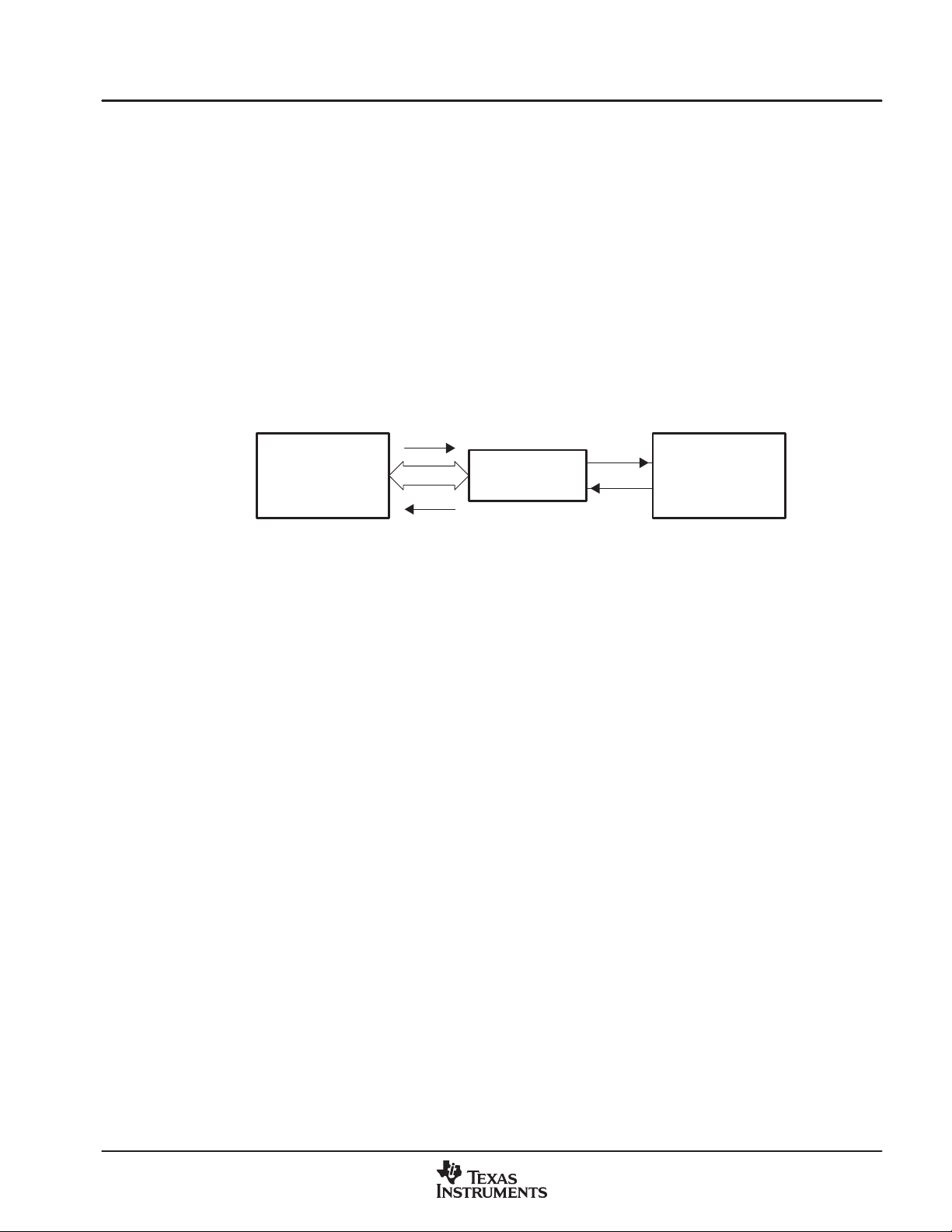
Host
(PC or On-The-Go
Dual-Role Device)
Out
USB
In
TUSB3410
Figure 1−1. Data Flow
SOUT
SIN
Legacy
Serial
Peripheral
SLLS519F—July 2007 TUSB3410
1
Page 10
Introduction
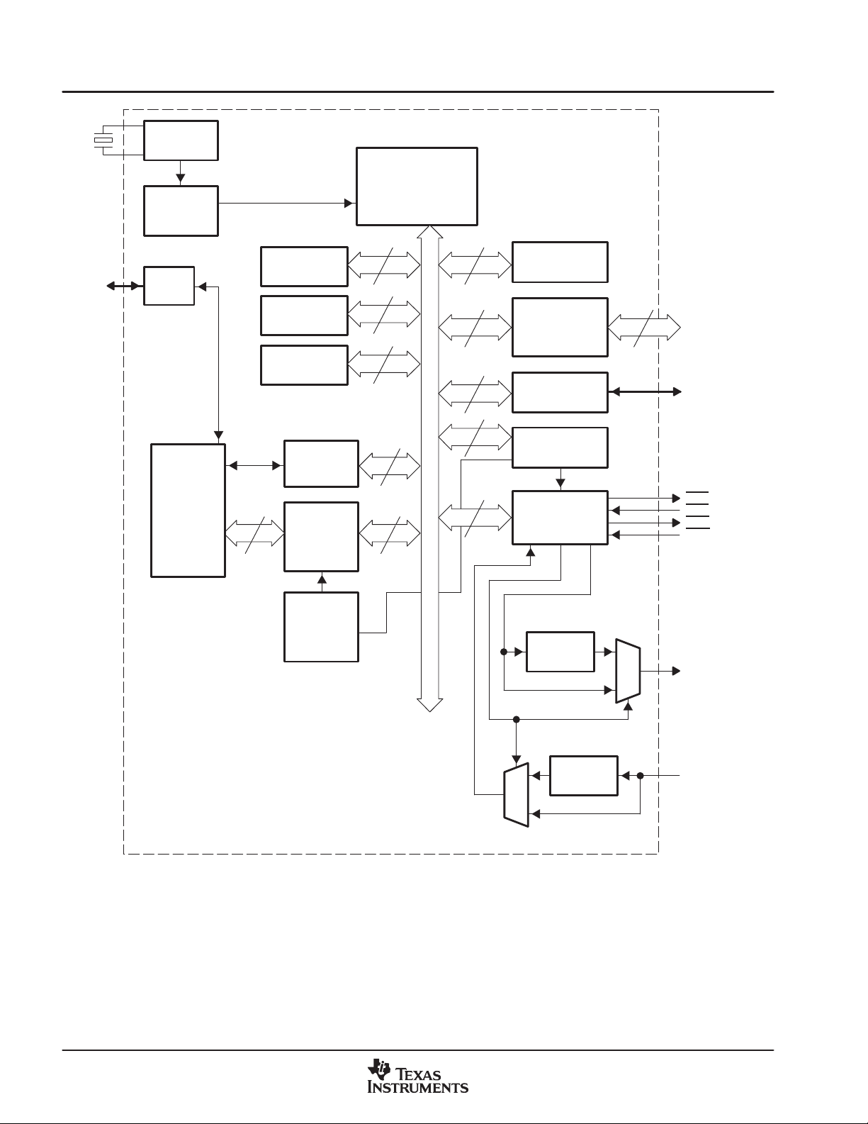
D
T
12 MHz
Clock
Oscillator
8052
PLL
and
Dividers
P, DM
USB
TxR
USB
Serial
Interface
Engine
24 MHz
10K × 8
ROM
16K × 8
RAM
2K × 8
SRAM
CPU-I/F
Suspend/
Resume
UBM
USB Buffer
Manager
Core
8 8
8
8
8
88
2 × 16-Bit
Timers
8 4
Port 3
8
8
8
SIN
I2C
Controller
DMA-1
DMA-3
UART−1
SOUT
P3.4
P3.3
P3.1
P3.0
I2C Bus
RTS
CTS
DTR
DSR
TDM
Control
Logic
M
U
X
IR
Encoder
Decoder
M
U
X
IR
Figure 1−2. USB-to-Serial (Single Channel) Controller Block Diagram
SOUT/IR_SOU
SIN/IR_SIN
2
SLLS519F—July 2007TUSB3410
Page 11
1.2 Ordering Information
T
COMMENT
A
−40°C to 85°C
0°C to 70°C
32-TERMINAL LQFP PACKAGE 32-TERMINAL QFN PACKAGE
TUSB3410 I VF TUSB3410 I RHB
TUSB3410 VF TUSB3410 RHB Shipped in trays
PACKAGED DEVICES
TUSB3410 I RHBR
Industrial temperature range
Shipped in trays
Industrial temperature range
Tape and Reel Option
TUSB3410 RHBR Tape and Reel Option
1.3 Revision History
Version Date Changes
Mar−2002 Initial Release
A Apr−2002 1. General grammatical corrections
B Jun−2002 1. Removed Design−in warning from cover sheet
C Nov−2003 1. Added Industrial Temperature Option and Information
D July 2005 1. General grammatical corrections
F July 2007 1. Added ordering information for TUSB3410IRHBR and TUSB3410RHBR
2. Added Design−in warning on cover sheet
3. Removed references to Optional preprogrammed VID/PID Registers from Section 5.1.6 through 5.1.11. Renumber the remainder of Section 5.1 accordingly – option no longer supported.
4. Clarified GPIO pin availability
2. Added Note 8 to Terminal Functions Table for GPIO Pins.
3. Removed Section 3.2.3 – Production Programming Mode – Mode no longer supported.
4. Added Clock Output Control description to section 5.1.5.
5. Removed Section 11.6.4 USB Descriptor with Binary Firmware
6. Added Icc Spec to Table 12.3
2. Added USB Logo to Cover
2. Numerous technical corrections
Introduction
SLLS519F—July 2007 TUSB3410
3
Page 12

Introduction
4
SLLS519F—July 2007TUSB3410
Page 13

2 Main Features
2.1 USB Features
• Fully compliant with USB 2.0 full speed specifications: TID #40340262
• Supports 12-Mbps USB data rate (full speed)
• Supports USB suspend, resume, and remote wakeup operations
• Supports two power source modes:
− Bus-powered mode
− Self-powered mode
• Can support a total of three input and three output (interrupt, bulk) endpoints
2.2 General Features
• Integrated 8052 microcontroller with
− 256 × 8 RAM for internal data
− 10K × 8 ROM (with USB and I
− 16K × 8 RAM for code space loadable from host or I2C port
− 2K × 8 shared RAM used for data buffers and endpoint descriptor blocks (EDB)
2
C boot loader)
Main Features
− Four GPIO terminals from 8052 port 3
2
− Master I
− MCU operates at 24 MHz providing 2 MIPS operation
− 128-ms watchdog timer
• Built-in two-channel DMA controller for USB/UART bulk I/O
• Operates from a 12-MHz crystal
• Supports USB suspend and resume
• Supports remote wake-up
• Available in 32-terminal LQFP
• 3.3-V operation with 1.8-V core operating voltage provided by on-chip 1.8-V voltage regulator
C controller for EEPROM device access
2.3 Enhanced UART Features
• Software/hardware flow control:
− Programmable Xon/Xoff characters
− Programmable Auto-RTS
• Automatic RS-485 bus transceiver control, with and without echo
• Selectable IrDA mode for up to 115.2 kbps transfer
/DTR and Auto-CTS/DSR
• Software selectable baud rate from 50 to 921.6 k baud
• Programmable serial-interface characteristics
− 5-, 6-, 7-, or 8-bit characters
− Even, odd, or no parity-bit generation and detection
− 1-, 1.5-, or 2-stop bit generation
SLLS519F—July 2007 TUSB3410
5
Page 14
Main Features
• Line break generation and detection
• Internal test and loop-back capabilities
• Modem-control functions (CTS
• Internal diagnostics capability
− Loopback control for communications link-fault isolation
− Break, parity, overrun, framing-error simulation
2.4 Terminal Assignment
, RTS, DSR, DTR, RI, and DCD)
VF PACKAGE
(TOP VIEW)
TEST1
TEST0
CLKOUT
DTR
RTS
SOUT/IR_SOUT
23 22 21 20 19
24 18
X2
25
26
27
28
29
30
31
32
12
3 4 5 6 7 8
VCC
X1/CLKI
GND
P3.4
P3.3
P3.1
P3.0
GND
SIN/IR_SIN
17
16
15
14
13
12
11
10
9
RI/CP
DCD
DSR
CTS
WAKEUP
SCL
SDA
RESET
VCC
VREGEN
SUSPEND
PUR
VDD18
DP
DM
GND
6
SLLS519F—July 2007TUSB3410
Page 15

Main Features
I/O
DESCRIPTION
Table 2−1. Terminal Functions
TERMINAL
NAME NO.
CLKOUT 22 O Clock output (controlled by bits 2 (CLKOUTEN) and 3(CLKSLCT) in the MODECNFG register (see
CTS 13 I UART: Clear to send (see Note 4)
DCD 15 I UART: Data carrier detect (see Note 4)
DM 7 I/O Upstream USB port differential data minus
DP 6 I/O Upstream USB port differential data plus
DSR 14 I UART: Data set ready (see Note 4)
DTR 21 O UART: Data terminal ready (see Note 1)
GND 8, 18, 28 GND Digital ground
P3.0 32 I/O General-purpose I/O 0 (port 3, terminal 0) (see Notes 3, 5, and 8)
P3.1 31 I/O General-purpose I/O 1 (port 3, terminal 1) (see Notes 3, 5, and 8)
P3.3 30 I/O General-purpose I/O 3 (port 3, terminal 3) (see Notes 3, 5, and 8)
P3.4 29 I/O General-purpose I/O 4 (port 3, terminal 4) (see Notes 3, 5, and 8)
PUR 5 O Pull-up resistor connection (see Note 2)
RESET 9 I Device master reset input (see Note 4)
RI/CP 16 I UART: Ring indicator (see Note 4)
RTS 20 O UART: Request to send (see Note 1)
SCL 11 O Master I2C controller: clock signal (see Note 1)
SDA 10 I/O Master I2C controller: data signal (see Notes 1 and 5)
SIN/IR_SIN 17 I UART: Serial input data / IR Serial data input (see Note 6)
SOUT/IR_SOUT 19 O UART: Serial output data / IR Serial data output (see Note 7)
SUSPEND 2 O Suspend indicator terminal (see Note 3). When this terminal is asserted high, the device is in
TEST0 23 I Test input (for factory test only) (see Note 5). This terminal must be tied to VCC through a 10-kΩ
TEST1 24 I Test input (for factory test only) (see Note 5). This terminal must be tied to VCC through a 10-kΩ
VCC 3, 25 PWR 3.3 V
VDD18 4 PWR 1.8-V supply. An internal voltage regulator generates this supply voltage when terminal VREGEN is
VREGEN 1 I This active-low terminal is used to enable the 3.3-V to 1.8-V voltage regulator.
WAKEUP 12 I Remote wake-up request terminal. When low, wakes up system (see Note 5)
X1/CLKI 27 I 12-MHz crystal input or clock input
X2 26 O 12-MHz crystal output
NOTES: 1. 3-state CMOS output (±4-mA drive/sink)
2. 3-state CMOS output (±8-mA drive/sink)
3. 3-state CMOS output (±12-mA drive/sink)
4. TTL-compatible, hysteresis input
5. TTL-compatible, hysteresis input, with internal 100-µA active pullup resistor
6. TTL-compatible input without hysteresis, with internal 100-µA active pullup resistor
7. Normal or IR mode: 3-state CMOS output (±4-mA drive/sink)
8. The MCU treats the outputs as open drain types in that the output can be driven low continuously, but a high output is driven for two
clock cycles and then the output is high impedance.
Section 5.5 and Note 1)
suspend mode.
resistor.
resistor.
low. When VREGEN
is high, 1.8 V must be supplied externally.
SLLS519F—July 2007 TUSB3410
7
Page 16

Main Features
8
SLLS519F—July 2007TUSB3410
Page 17

3 Detailed Controller Description
3.1 Operating Modes
The TUSB3410 controls its USB interface in response to USB commands, and this action is independent of
the serial port mode selected. On the other hand, the serial port can be configured in three different modes.
As with any interface device, data movement is the main function of the TUSB3410, but typically the initial
configuration and error handling consume most of the support code. The following sections describe the
various modes the device can be used in and the means of configuring the device.
3.2 USB Interface Configuration
The TUSB3410 contains onboard ROM microcode, which enables the MCU to enumerate the device as a USB
peripheral. The ROM microcode can also load application code into internal RAM from either external memory
via the I
3.2.1 External Memory Case
After reset, the TUSB3410 is disconnected from the USB. Bit 7 (CONT) in the USBCTL register (see
Section 5.4) is cleared. The TUSB3410 checks the I
then it uploads the code from the external memory device into the RAM program space. Once loaded, the
TUSB3410 connects to the USB by setting the CONT bit and enumeration and configuration are performed.
This is the most likely use of the device.
3.2.2 Host Download Case
If the valid code is not found at the I2C port, then the TUSB3410 connects to the USB by setting bit 7 (CONT)
in the USBCTL register (see Section 5.4), and then an enumeration and default configuration are performed.
The host can download additional microcode into RAM to tailor the application. Then, the MCU causes a
disconnect and reconnect by clearing and setting the CONT bit, which causes the TUSB3410 to be
re-enumerated with a new configuration.
2
C bus or from the host via the USB.
Detailed Controller Description
2
C port for the existence of valid code; if it finds valid code,
3.3 USB Data Movement
From the USB perspective, the TUSB3410 looks like a USB peripheral device. It uses endpoint 0 as its control
endpoint, as do all USB peripherals. It also configures up to three input and three output endpoints, although
most applications use one bulk input endpoint for data in, one bulk output endpoint for data out, and one
interrupt endpoint for status updates. The USB configuration likely remains the same regardless of the serial
port configuration.
Most data is moved from the USB side to the UART side and from the UART side to the USB side using on-chip
DMA transfers. Some special cases may use programmed I/O under control of the MCU.
3.4 Serial Port Setup
The serial port requires a few control registers to be written to configure its operation. This configuration likely
remains the same regardless of the data mode used. These registers include the line control register that
controls the serial word format and the divisor registers that control the baud rate.
These registers are usually controlled by the host application.
3.5 Serial Port Data Modes
The serial port can be configured in three different, although similar, data modes: the RS-232 data mode, the
RS-485 data mode, and the IrDA data mode. Similar to the USB mode, once configured for a specific
application, it is unlikely that the mode would be changed. The different modes affect the timing of the serial
input and output or the use of the control signals. However, the basic serial-to-parallel conversion of the
receiver and parallel-to-serial conversion of the transmitter remain the same in all modes. Some features are
available in all modes, but are only applicable in certain modes. For instance, software flow control via Xoff/Xon
characters can be used in all modes, but would usually only be used in RS-232 or IrDA mode because the
RS-485 mode is half-duplex communication. Similarly, hardware flow control via RTS
handshaking is available in RS-232 or IrDA mode. However, this would probably be used only in RS-232 mode,
since in IrDA mode only the SIN and SOUT paths are optically coupled.
/CTS (or DTR/DSR)
SLLS519F—July 2007 TUSB3410
9
Page 18

Detailed Controller Description
3.5.1 RS-232 Data Mode
The default mode is called the RS-232 mode and is typically used for full duplex communication on SOUT and
SIN. In this mode, the modem control outputs (RTS
outputs. The modem control inputs (CTS
inputs. Alternatively , R TS
receive FIFO overruns. Finally, software flow control via Xoff/Xon characters can be used for the same
purpose.
This mode represents the most general-purpose applications, and the other modes are subsets of this mode.
3.5.2 RS-485 Data Mode
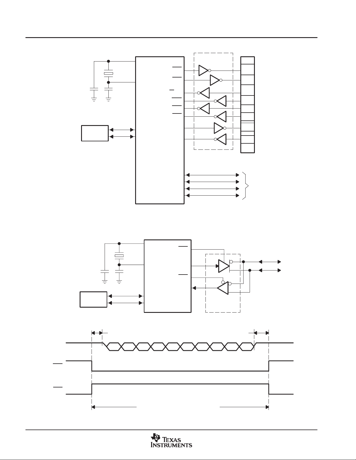
The RS-485 mode is very similar to the RS-232 mode in that the SOUT and SIN formats remain the same.
Since RS-485 is a bus architecture, it is inherently a single duplex communication system. The TUSB3410
in RS-485 mode controls the RTS
receiver. When in RS-485 mode, the enable signals for transmitting are automatically asserted whenever the
DMA is set up for outbound data. The receiver can be left enabled while the driver is enabled to allow an echo
if desired, but when receive data is expected, the driver must be disabled. Note that this precludes use of
hardware flow control, since this is a half-duplex operation, it would not be effective. Software flow control is
supported, but may be of limited value.
The RS-485 mode is enabled by setting bit 7 (485E) in the FCRL register (see Section 7.1.4), and bit 1 (RCVE)
in the MCR register (see Section 7.1.6) allows the receiver to eavesdrop while in the RS-485 mode.
and DTR) communicate to a modem or are general
, DSR, DCD, and RI/CP) communicate to a modem or are general
and CTS (or DTR and DSR) can throttle the data flow on SOUT and SIN to prevent
and DTR signals such that either can enable an RS-485 driver or RS-485
3.5.3 IrDA Data Mode
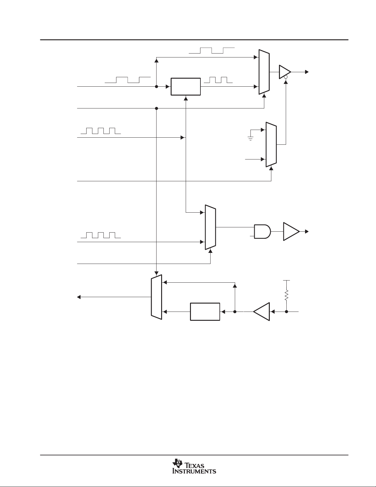
The IrDA mode encodes SOUT and decodes SIN in the manner prescribed by the IrDA standard, up to
115.2 kbps. Connection to an external IrDA transceiver is required. Communications is usually full duplex.
Generally , i n a n IrDA system, only the SOUT and SIN paths are connected so hardware flow control is usually
not an option. Software flow control is supported.
The IrDA mode is enabled by setting bit 6 (IREN) in the USBCTL register (see Section 5.4).
The IR encoder and decoder circuitry work with the UART to change the serial bit stream into a series of pulses
and back again. For every zero bit in the outbound serial stream, the encoder sends a low-to-high-to-low pulse
with the duration of 3/16 of a bit frame at the middle of the bit time. For every one bit in the serial stream, the
output remains low for the entire bit time.
The decoding process consists of receiving the signal from the IrDA receiver and converting it into a series
of zeroes and ones. As the converse to the encoder, the decoder converts a pulse to a zero bit and the lack
of a pulse to a one bit.
10
SLLS519F—July 2007TUSB3410
Page 19
Detailed Controller Description
T
From
UART
IREN (in
USBCTL
Register)
UART
BaudOut
Clock
TXCNTL (in
MODECNFG
Register)
3.556 MHz
CLKSLCT (in
MODECNFG
Register)
To
UART
Receiver
SOUT
SIN
SOUT
IR
Encoder
SOFTSW (in
MODECNFG
Register)
0
M
U
X
CLKOUTEN
1
MODECNFG
0
M
U
X
IR_RX
1
IR
Decoder
IR_TX
(in
Register)
0
M
U
X
1
0
M
U
X
1
3.3 V
SOUT/IR_SOU
Terminal
CLKOUT
Terminal
SIN/IR_SIN
Terminal
Figure 3−1. RS-232 and IR Mode Select
SLLS519F—July 2007 TUSB3410
11
Page 20
Detailed Controller Description
12 MHz
X1/CLKI
DTR
DB9
Connector
Transceivers
4
RTS
RI/CP
DCD
DSR
CTS
SOUT
SIN
P3.0
P3.1
P3.3
P3.4
USB-0
X2
DP
DM
TUSB3410
Figure 3−2. USB-to-Serial Implementation (RS-232)
12 MHz
X1/CLKI
RTS
7
1
Serial Port
6
8
3
2
GPIO Terminals for
Other Onboard
Control Function
RS-485 Bus
SOUT
DTR
RTS
USB-0
X2
DP
DM
TUSB3410
2-Bit Time 1-Bit Max
Receiver is Disabled if RCVE = 0
SOUT
DTR
SIN
RS-485
Transceiver
Figure 3−3. RS-485 Bus Implementation
12
SLLS519F—July 2007TUSB3410
Page 21
4 MCU Memory Map
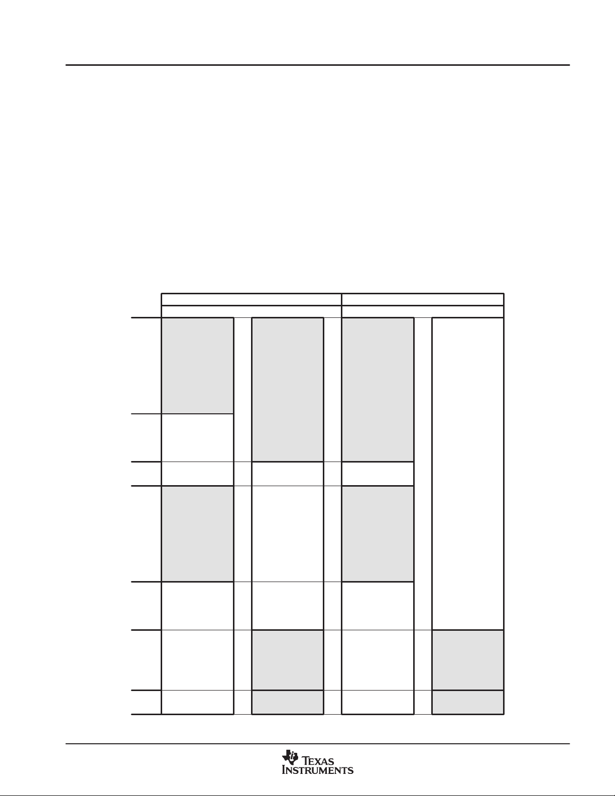
Figure 4−1 illustrates the MCU memory map under boot and normal operation.
The internal 256 bytes of RAM are not shown, since they are assumed to be in the standard
8052 location (0000h to 00FFh). The shaded areas represent the internal ROM/RAM.
• When bit 0 (SDW) of the ROMS register is 0 (boot mode)
The 10K ROM is mapped to address (0x0000−0x27FF) and is duplicated in location (0x8000−0xA7FF) in
code space. The internal 16K RAM is mapped to address range (0x0000−0x3FFF) in data space. Buffers,
MMR, and I/O are mapped to address range (0xF800−0xFFFF) in data space.
• When bit 0 (SDW) is 1 (normal mode)
The 10K ROM is mapped to (0x8000−0xA7FF) in code space. The internal 16K RAM is mapped to
address range (0x0000−0x3FFF) in code space. Buffers, MMR, and I/O are mapped to address range
(0xF800−0xFFFF) in data space.
MCU Memory Map
NOTE:
0000h
27FFh
3FFFh
8000h
A7FFh
Boot Mode (SDW = 0)
CODE XDATA
10K Boot ROM
10K Boot ROM
(16K)
Read/Write
Normal Mode (SDW = 1)
CODE XDATA
16K
Code RAM
Read Only
10K Boot ROM
F800h
2K Data
MMR
FF7Fh
FF80h
FFFFh
2K Data
MMR
Figure 4−1. MCU Memory Map
SLLS519F—July 2007 TUSB3410
13
Page 22
MCU Memory Map
0
SDW
0
BOOT ROM
RAM CODE
ROM CODE
4.1 Miscellaneous Registers
4.1.1 ROMS: ROM Shadow Configuration Register (Addr:FF90h)
This register is used by the MCU to switch from boot mode to normal operation mode (boot mode is set on
power-on reset only). In addition, this register provides the device revision number and the ROM/RAM
configuration.
765 4 32 1 0
ROA S1 S0 RSVD RSVD RSVD RSVD SDW
R/O R/O R/O R/O R/O R/O R/O R/W
BIT
4−1 RSVD No effect These bits are always read as 0000b.
6−5 S[1:0] No effect Code space size. These bits define the ROM or RAM code-space size (bit 7 (ROA) defines ROM or
NAME RESET FUNCTION
0 SDW 0
7 ROA No effect ROM or RAM version. This bit indicates whether the code space is RAM or ROM based. This bit is
This bit enables/disables boot ROM. (Shadow the ROM).
SDW = 0 When clear, the MCU executes from the 10K boot ROM space. The boot ROM appears in two
locations: 0000 h and 8000h. The 16K RAM is mapped to XDATA space; therefore, a read/write
operation is possible. This bit is set by the MCU after the RAM load is completed. The MCU
cannot clear this bit; it is cleared on power-up reset or watchdog time-out reset.
SDW = 1 When set by the MCU, the 10K boot ROM maps to location 8000h, and the 16K RAM is mapped
to code space, starting at location 0000h. At this point, the MCU executes from RAM, and the
write operation is disabled (no write operation is possible in code space).
RAM). These bits are permanently set to 10b, indicating 16K bytes of code space, and are not affected
by reset (see Table 4−1).
00 = 4K bytes code space size
01 = 8K bytes code space size
10 = 16K bytes code space size
11 = 32K bytes code space size
permanently set to 1, indicating the code space is RAM, and is not affected by reset (see Table 4−1).
ROA = 0 Code space is ROM
ROA = 1 Code space is RAM
Table 4−1. ROM/RAM Size Definition Table
ROMS REGISTER
ROA S1 S0
0 0 0 None None 4K
0 0 1 None None 8K
0 1 0 None None 16K (reserved)
1 1 1 None None 32K (reserved)
1 0 0 10K 4K None
1 0 1 10K 8K None
†
†
1
1
1 1 1 10K 32K (reserved) None
†
This is the hardwired setting.
†
0
10K
†
16K
†
None
†
4.1.2 Boot Operation (MCU Firmware Loading)
Since the code space is in RAM (with the exception of the boot ROM), the TUSB3410 firmware must be loaded
from an external source. Two sources are available for booting: one from an external serial EEPROM
connected to the I
register (see Section 4.1.1) and bit 7 (CONT) in the USBCTL register (see Section 5.4) are cleared. This
configures the memory space to boot mode (see Table 4−3) and keeps the device disconnected from the host.
The first instruction is fetched from location 0000h (which is in the 10K ROM). The 16K RAM is mapped to
XDATA space (location 0000h). The MCU executes a read from an external EEPROM and tests whether it
contains the code (by testing for boot signature). If it contains the code, then the MCU reads from EEPROM
14
2
C bus and the other from the host via the USB. On device reset, bit 0 (SDW) in the ROMS
SLLS519F—July 2007TUSB3410
Page 23
MCU Memory Map
and writes to the 16K RAM in XDATA space. If it does not contain the code, then the MCU proceeds to boot
from the USB.
Once the code is loaded, the MCU sets the SDW bit to 1 in the ROMS register . This switches the memory map
to normal mode; that is, the 16K RAM is mapped to code space, and the MCU starts executing from location
0000h. Once the switch is done, the MCU sets the CONT bit to 1 in the USBCTL register. This connects the
device to the USB and results in normal USB device enumeration.
4.1.3 WDCSR: Watchdog Timer, Control, and Status Register (Addr:FF93h)
A watchdog timer (WDT) with 1-ms clock is provided. If this register is not accessed for a period of 128 ms,
then the WDT counter resets the MCU (see Figure 5−1). The watchdog timer is enabled by default and can
be disabled by writing a pattern of 101010b into the WDD[5:0] bits. The 1-ms clock for the watchdog timer is
generated from the SOF pulses. Therefore, in order for the watchdog timer to count, bit 7 (CONT) in the
USBCTL register (see Section 5.4) must be set.
765 4 32 1 0
WDD0 WDR WDD5 WDD4 WDD3 WDD2 WDD1 WDT
R/W R/C R/W R/W R/W R/W R/W W/O
BIT
5−1 WDD[5:1] 00000 These bits disable the watchdog timer. For the timer to be disabled these bits must be set to 10101b and
NAME RESET FUNCTION
0 WDT 0 MCU must write a 1 to this bit to prevent the watchdog timer from resetting the MCU. If the MCU does not
6 WDR 0
7 WDD0 1 This bit is one of the six disable bits for the watchdog timer. This bit must be cleared in order for the
write a 1 in a period of 128 ms, the watchdog timer resets the device. Writing a 0 has no effect on the
watchdog timer. (The watchdog timer is a 7-bit counter using a 1-ms CLK.) This bit is read as 0.
bit 7 (WDD0) must also be set to 0. If any other pattern is present, then the watchdog timer is in operation.
Watchdog reset indication bit. This bit indicates if the reset occurred due to power-on reset or watchdog
timer reset.
WDR = 0 A power-up reset occurred
WDR = 1 A watchdog time-out reset occurred. To clear this bit, the MCU must write a1. Writing a 0 has no
effect.
watchdog timer to be disabled.
4.2 Buffers + I/O RAM Map
The address range from F800h to FFFFh (2K bytes) is reserved for data buffers, setup packet, endpoint
descriptors block (EDB), and all I/O. There are 128 locations reserved for memory-mapped registers (MMR).
Table 4−2 represents the XDATA space allocation and access restriction for the DMA, USB buffer manager
(UBM), and MCU.
Table 4−2. XDATA Space
DESCRIPTION ADDRESS RANGE UBM ACCESS DMA ACCESS MCU ACCESS
Internal MMRs
(Memory-Mapped Registers)
EDB
(Endpoint Descriptors Block)
Setup Packet FF07h−FF00h Yes No Yes
Input Endpoint-0 Buffer FEFFh−FEF8h Yes Yes Yes
Output Endpoint-0 Buffer FEF7h−FEF0h Yes Yes Yes
Data Buffers FEEFh−F800h Yes Yes Yes
FFFFh−FF80h
FF7Fh−FF08h Only for EDB update Only for EDB update Yes
No
(Only EDB-0)
(only data register and EDB-0)
No
Yes
SLLS519F—July 2007 TUSB3410
15
Page 24
MCU Memory Map
Table 4−3. Memory-Mapped Registers Summary (XDATA Range = FF80h → FFFFh)
ADDRESS REGISTER DESCRIPTION
FFFFh FUNADR Function address register
FFFEh USBSTA USB status register
FFFDh USBMSK USB interrupt mask register
FFFCh USBCTL USB control register
FFFBh MODECNFG Mode configuration register
FFFAh−FFF4h Reserved
FFF3h I2CADR I2C-port address register
FFF2h I2CDATI I2C-port data input register
FFF1h I2CDATO I2C-port data output register
FFF0h I2CSTA I2C-port status register
FFEFh SERNUM7 Serial number byte 7 register
FFEEh SERNUM6 Serial number byte 6 register
FFEDh SERNUM5 Serial number byte 5 register
FFECh SERNUM4 Serial number byte 4 register
FFEBh SERNUM3 Serial number byte 3 register
FFEAh SERNUM2 Serial number byte 2 register
FFE9h SERNUM1 Serial number byte 1 register
FFE8h SERNUM0 Serial number byte 0 register
FFE7h−FFE6h Reserved
FFE5h DMACSR3 DMA-3: Control and status register
FFE4h DMACDR3 DMA-3: Channel definition register
FFE3h−FFE2h Reserved
FFE1h DMACSR1 DMA-1: Control and status register
FFE0h DMACDR1 DMA-1: Channel definition register
FFDFh−FFACh Reserved
FFABh MASK UART: Interrupt mask register
FFAAh XOFF UART: Xoff register
FFA9h XON UART: Xon register
FFA8h DLH UART: Divisor high-byte register
FFA7h DLL UART: Divisor low-byte register
FFA6h MSR UART: Modem status register
FFA5h LSR UART: Line status register
FFA4h MCR UART: Modem control register
FFA3h FCRL UART: Flow control register
FFA2h LCR UART: Line control registers
FFA1h TDR UART: Transmitter data registers
FFA0h RDR UART: Receiver data registers
FF9Eh PUR_3 GPIO: Pullup register for port 3
16
SLLS519F—July 2007TUSB3410
Page 25

MCU Memory Map
Table 4−3. Memory-Mapped Registers Summary (XDATA Range = FF80h → FFFFh) (Continued)
ADDRESS REGISTER DESCRIPTION
FF9Dh−FF94h
FF93h
FF92h VECINT Vector interrupt register
FF91h Reserved
FF90h ROMS ROM shadow configuration register
FF8Fh−FF84h Reserved
FF83h OEPBCNT_0 Output endpoint_0: Byte count register
FF82h OEPCNFG_0 Output endpoint_0: Configuration register
FF81h IEPBCNT_0 Input endpoint_0: Byte count register
FF80h IEPCNFG_0 Input endpoint_0: Configuration register
Reserved
WDCSR
Watchdog timer control and status register
Table 4−4. EDB Memory Locations
ADDRESS REGISTER DESCRIPTION
FF7Fh−FF60h Reserved
FF5Fh IEPSIZXY_3 Input endpoint_3: X-Y buffer size
FF5Eh IEPBCTY_3 Input endpoint_3: Y-byte count
FF5Dh IEPBBAY_3 Input endpoint_3: Y-buffer base address
FF5Ch − Reserved
FF5Bh − Reserved
FF5Ah IEPBCTX_3 Input endpoint_3: X-byte count
FF59h IEPBBAX Input endpoint_3: X-buffer base address
FF58h IEPCNF_3 Input endpoint_3: Configuration
FF57h IEPSIZXY_2 Input endpoint_2: X-Y buffer size
FF56h IEPBCTY_2 Input endpoint_2: Y-byte count
FF55h IEPBBAY_2 Input endpoint_2: Y-buffer base address
FF54h − Reserved
FF53h − Reserved
FF52h IEPBCTX_2 Input endpoint_2: X-byte count
FF51h IEPBBAX_2 Input endpoint_2: X-buffer base address
FF50h IEPCNF_2 Input endpoint_2: Configuration
FF4Fh IEPSIZXY_1 Input endpoint_1: X-Y buffer size
FF4Eh IEPBCTY_1 Input endpoint_1: Y-byte count
FF4Dh IEPBBAY_1 Input endpoint_1: Y-buffer base address
FF4Ch − Reserved
FF4Bh − Reserved
FF4Ah IEPBCTX_1 Input endpoint_1: X-byte count
FF49h IEPBBAX_1 Input endpoint_1: X-buffer base address
FF48h IEPCNF_1 Input endpoint_1: Configuration
FF47h
↑ Reserved
FF20h
FF1Fh OEPSIZXY_3 Output endpoint_3: X-Y buffer size
FF1Eh OEPBCTY_3 Output endpoint_3: Y-byte count
FF1Dh OEPBBAY_3 Output endpoint_3: Y-buffer base address
FF1Bh−FF1Ch − Reserved
SLLS519F—July 2007 TUSB3410
17
Page 26

MCU Memory Map
↑
Table 4−4. EDB Memory Locations (Continued)
ADDRESS REGISTER DESCRIPTION
FF1Ah OEPBCTX_3 Output endpoint_3: X-byte count
FF19h OEPBBAX_3 Output endpoint_3: X-buffer base address
FF18h OEPCNF_3 Output endpoint_3: Configuration
FF17h OEPSIZXY_2 Output endpoint_2: X-Y buffer size
FF16h OEPBCTY_2 Output endpoint_2: Y-byte count
FF15h OEPBBAY_2 Output endpoint_2: Y-buffer base address
FF14h−FF13h − Reserved
FF12h OEPBCTX_2 Output endpoint_2: X-byte count
FF11h OEPBBAX_2 Output endpoint_2: X-buffer base address
FF10h OEPCNF_2 Output endpoint_2: Configuration
FF0Fh OEPSIZXY_1 Output endpoint_1: X-Y buffer size
FF0Eh OEPBCTY_1 Output endpoint_1: Y-byte count
FF0Dh OEPBBAY_1 Output endpoint_1: Y -buffer base address
FF0Ch−FF0Bh − Reserved
FF0Ah OEPBCTX_1 Output endpoint_1: X-byte count
FF09h OEPBBAX_1 Output endpoint_1: X-buffer base address
FF08h OEPCNF_1 Output endpoint_1: Configuration
FF07h
↑ (8 bytes) Setup packet block
FF00h
FEFFh
↑ (8 bytes) Input endpoint_0 buffer
FEF8h
FEF7h
↑ (8 bytes) Output endpoint_0 buffer
FEF0h
FEEFh TOPBUFF Top of buffer space
↑
F800h STABUFF Start of buffer space
Buffer space
4.3 Endpoint Descriptor Block (EDB−1 to EDB−3)
Data transfers between the USB, the MCU, and external devices that are defined by an endpoint descriptor
block (EDB). Three input and three output EDBs are provided. With the exception of EDB-0 (I/O endpoint-0),
all EDBs are located in SRAM as per Table 4−3. Each EDB contains information describing the X- and
Y-buffers. In addition, each EDB provides general status information.
Table 4−5 describes the EDB entries for EDB−1 to EDB−3. EDB−0 registers are described in Table 4−6.
18
SLLS519F—July 2007TUSB3410
Page 27
MCU Memory Map
3
STALL
0
Table 4−5. Endpoint Registers and Offsets in RAM (n = 1 to 3)
OFFSET ENTRY NAME DESCRIPTION
07 EPSIZXY_n I/O endpoint_n: X/Y-buffer size
06 EPBCTY_n I/O endpoint_n: Y-byte count
05 EPBBAY_n I/O endpoint_n: Y-buffer base address
04 SPARE Not used
03 SPARE Not used
02 EPBCTX_n I/O endpoint_n: X-byte count
01 EPBBAX_n I/O endpoint_n: X-buffer base address
00 EPCNF_n I/O endpoint_n: Configuration
Table 4−6. Endpoint Registers Base Addresses
BASE ADDRESS DESCRIPTION
FF08h Output endpoint 1
FF10h Output endpoint 2
FF18h Output endpoint 3
FF48h Input endpoint 1
FF50h Input endpoint 2
FF58h Input endpoint 3
4.3.1 OEPCNF_n: Output Endpoint Configuration (n = 1 to 3) (Base Addr: FF08h, FF10h,
FF18h)
765 4 32 1 0
UBME ISO=0 TOGLE DBUF STALL USBIE RSV RSV
R/W R/W R/W R/W R/W R/W R/W R/W
BIT NAME RESET FUNCTION
1−0 RSV x Reserved = 0
2 USBIE x USB interrupt enable on transaction completion. Set/cleared by the MCU.
3 STALL 0
4 DBUF x Double-buffer enable. Set/cleared by the MCU.
5 TOGLE x USB toggle bit. This bit reflects the toggle sequence bit of DATA0, DATA1.
6 ISO x ISO = 0 Nonisochronous transfer. This bit must be cleared by the MCU since only nonisochronous transfer
7 UBME x USB buffer manager (UBM) enable/disable bit. Set/cleared by the MCU.
USBIE = 0 No interrupt on transaction completion
USBIE = 1 Interrupt on transaction completion
USB stall condition indication. Set/cleared by the MCU.
STALL = 0
STALL = 1
DBUF = 0 Primary buffer only (X-buffer only)
DBUF = 1 Toggle bit selects buffer
is supported.
UBME = 0 UBM cannot use this endpoint
UBME = 1 UBM can use this endpoint
No stall
USB stall condition. If set by the MCU, then a STALL handshake is initiated and the bit is
cleared by the MCU.
4.3.2 OEPBBAX_n: Output Endpoint X-Buffer Base Address (n = 1 to 3) (Offset 1)
765 4 32 1 0
A10 A9 A8 A7 A6 A5 A4 A3
R/W R/W R/W R/W R/W R/W R/W R/W
BIT
7−0 A[10:3] x A[10:3] of X-buffer base address (padded with 3 LSBs of zeros for a total of 11 bits). This value is set by
SLLS519F—July 2007 TUSB3410
NAME RESET FUNCTION
the MCU. The UBM or DMA uses this value as the start-address of a given transaction. Note that the UBM
or DMA does not change this value at the end of a transaction.
19
Page 28
MCU Memory Map
4.3.3 OEPBCTX_n: Output Endpoint X Byte Count (n = 1 to 3) (Offset 2)
765 4 32 1 0
NAK C6 C5 C4 C3 C2 C1 C0
R/W R/W R/W R/W R/W R/W R/W R/W
BIT NAME RESET FUNCTION
6−0 C[6:0] x X-buffer byte count:
7 NAK x NAK = 0
X000.0000b Count = 0
X000.0001b Count = 1 byte
:
:
X011.1111b Count = 63 bytes
X100.0000b Count = 64 bytes
Any value ≥ 100.0001b may result in unpredictable results.
NAK = 1
No valid data in buffer. Ready for host OUT
Buffer contains a valid packet from host (gives NAK response to Host OUT request)
4.3.4 OEPBBAY_n: Output Endpoint Y-Buffer Base Address (n = 1 to 3) (Offset 5)
765 4 32 1 0
A10
R/W R/W R/W R/W R/W R/W R/W R/W
A9 A8 A7 A6 A5 A4 A3
BIT
7−0 A[10:3] x A[10:3] of Y-buffer base address (padded with 3 LSBs of zeros for a total of 11 bits). This value is set by
NAME RESET FUNCTION
the MCU. The UBM or DMA uses this value as the start-address of a given transaction. Furthermore, UBM
or DMA does not change this value at the end of a transaction.
4.3.5 OEPBCTY_n: Output Endpoint Y-Byte Count (n = 1 to 3) (Offset 6)
765 4 32 1 0
NAK
R/W R/W R/W R/W R/W R/W R/W R/W
BIT
6−0 C[6:0] x Y-byte count:
7 NAK x NAK = 0
NAME RESET FUNCTION
C6 C5 C4 C3 C2 C1 C0
X000.0000b Count = 0
X000.0001b Count = 1 byte
:
:
X011.1111b Count = 63 bytes
X100.0000b Count = 64 bytes
Any value ≥ 100.0001b may result in unpredictable results.
NAK = 1
No valid data in buffer. Ready for host OUT
Buffer contains a valid packet from host (gives NAK response to Host OUT request)
20
SLLS519F—July 2007TUSB3410
Page 29
MCU Memory Map
4.3.6 OEPSIZXY_n: Output Endpoint X-/Y-Buffer Size (n = 1 to 3) (Offset 7)
765 4 32 1 0
RSV
R/W R/W R/W R/W R/W R/W R/W R/W
S6 S5 S4 S3 S2 S1 S0
BIT
6−0 S[6:0] x X- and Y-buffer size:
7 RSV x Reserved = 0
NAME RESET FUNCTION
0000.0000b Size = 0
0000.0001b Size = 1 byte
:
:
0011.1111b Size = 63 bytes
0100.0000b Size = 64 bytes
Any value ≥ 100.0001b may result in unpredictable results.
4.3.7 IEPCNF_n: Input Endpoint Configuration (n = 1 to 3) (Base Addr: FF48h, FF50h,
FF58h)
765 4 32 1 0
UBME ISO=0 TOGLE DBUF STALL USBIE RSV RSV
R/W R/W R/W R/W R/W R/W R/W R/W
BIT
1−0 RSV x Reserved = 0
2 USBIE x USB interrupt enable on transaction completion
3 STALL 0 USB stall condition indication. Set by the UBM but can be set/cleared by the MCU
4 DBUF x Double buffer enable
5 TOGLE x USB toggle bit. This bit reflects the toggle sequence bit of DATA0, DATA1
6 ISO x ISO = 0 Nonisochronous transfer. This bit must be cleared by the MCU since only nonisochronous
7 UBME x UBM enable/disable bit. Set/cleared by the MCU
NAME RESET FUNCTION
USBIE = 0 No interrupt on transaction completion
USBIE = 1 Interrupt on transaction completion
STALL = 0 No stall
STALL = 1 USB stall condition. If set by the MCU, then a STALL handshake is initiated and the bit is
cleared automatically.
DBUF = 0 Primary buffer only (X-buffer only)
DBUF = 1 Toggle bit selects buffer
transfer is supported
UBME = 0 UBM cannot use this endpoint
UBME = 1 UBM can use this endpoint
4.3.8 IEPBBAX_n: Input Endpoint X-Buffer Base Address (n = 1 to 3) (Offset 1)
765 4 32 1 0
A10
R/W R/W R/W R/W R/W R/W R/W R/W
BIT
7−0 A[10:3] x A[10:3] of X-buffer base address (padded with 3 LSBs of zeros for a total of 11 bits). This value is set by
SLLS519F—July 2007 TUSB3410
NAME RESET FUNCTION
A9 A8 A7 A6 A5 A4 A3
the MCU. The UBM or DMA uses this value as the start-address of a given transaction, but note that the
UBM or DMA does not change this value at the end of a transaction.
21
Page 30

MCU Memory Map
4.3.9 IEPBCTX_n: Input Endpoint X-Byte Count (n = 1 to 3) (Offset 2)
765 4 32 1 0
NAK C6 C5 C4 C3 C2 C1 C0
R/W R/W R/W R/W R/W R/W R/W R/W
BIT NAME RESET FUNCTION
6−0 C[6:0] x X-Buffer byte count:
7 NAK x NAK = 0
X000.0000b Count = 0
X000.0001b Count = 1 byte
:
:
X011.1111b Count = 63 bytes
X100.0000b Count = 64 bytes
Any value ≥ 100.0001b may result in unpredictable results.
NAK = 1
Buffer contains a valid packet for host-IN transaction
Buffer is empty (gives NAK response to host-IN request)
4.3.10 IEPBBAY_n: Input Endpoint Y-Buffer Base Address (n = 1 to 3) (Offset 5)
765 4 32 1 0
A10
R/W R/W R/W R/W R/W R/W R/W R/W
A9 A8 A7 A6 A5 A4 A3
BIT
7−0 A[10:3] x A[10:3] of Y-buffer base address (padded with 3 LSBs of zeros for a total of 11 bits). This value is set by
NAME RESET FUNCTION
the MCU. The UBM or DMA uses this value as the start-address of a given transaction, but note that the
UBM or DMA does not change this value at the end of a transaction.
4.3.11 IEPBCTY_n: Input Endpoint Y-Byte Count (n = 1 to 3) (Offset 6)
765 4 32 1 0
NAK
R/W R/W R/W R/W R/W R/W R/W R/W
BIT
6−0 C[6:0] x Y-Byte count:
7 NAK x NAK = 0
NAME RESET FUNCTION
C6 C5 C4 C3 C2 C1 C0
X000.0000b Count = 0
X000.0001b Count = 1 byte
:
:
X011.1111b Count = 63 bytes
X100.0000b Count = 64 bytes
Any value ≥ 100.0001b may result in unpredictable results.
NAK = 1
Buffer contains a valid packet for host-IN transaction
Buffer is empty (gives NAK response to host-IN request)
22
SLLS519F—July 2007TUSB3410
Page 31

MCU Memory Map
4.3.12 IEPSIZXY_n: Input Endpoint X-/Y-Buffer Size (n = 1 to 3) (Offset 7)
765 4 32 1 0
RSV
R/W R/W R/W R/W R/W R/W R/W R/W
S6 S5 S4 S3 S2 S1 S0
BIT
6−0 S[6:0] x X- and Y-buffer size:
7 RSV x Reserved = 0
NAME RESET FUNCTION
0000.0000b Size = 0
0000.0001b Size = 1 byte
:
:
0011.1111b Size = 63 bytes
0100.0000b Size = 64 bytes
Any value ≥ 100.0001b may result in unpredictable results.
4.4 Endpoint-0 Descriptor Registers
Unlike registers EDB-1 to EDB-3, which are defined as memory entries in SRAM, endpoint-0 is described by
a set of four registers (two for output and two for input). The registers and their respective addresses, used
for EDB-0 description, are defined in Table 4−7. EDB-0 has no buffer base-address register, since these
addresses are hardwired to FEF8h and FEF0h. Note that the bit positions have been preserved to provide
consistency with EDB-n (n = 1 to 3).
Table 4−7. Input/Output EDB-0 Registers
ADDRESS REGISTER NAME DESCRIPTION BUFFER BASE ADDRESS
FF83h
FF82h
FF81h
FF80h
OEPBCNT_0
OEPCNFG_0
IEPBCNT_0
IEPCNFG_0
Output endpoint_0: Byte count register
Output endpoint_0: Configuration register
Input endpoint_0: Byte count register
Input endpoint_0: Configuration register
FEF0h
FEF8h
4.4.1 IEPCNFG_0: Input Endpoint-0 Configuration Register (Addr:FF80h)
765 4 32 1 0
UBME RSV TOGLE RSV STALL USBIE RSV RSV
R/W R/O R/O R/O R/W R/W R/O R/O
BIT
1−0 RSV 0 Reserved = 0
2 USBIE 0 USB interrupt enable on transaction completion. Set/cleared by the MCU.
3 STALL 0 USB stall condition indication. Set/cleared by the MCU
4 RSV 0 Reserved = 0
5 TOGLE 0 USB toggle bit. This bit reflects the toggle sequence bit of DATA0, DATA1.
6 RSV 0 Reserved = 0
7 UBME 0 UBM enable/disable bit. Set/cleared by the MCU
SLLS519F—July 2007 TUSB3410
NAME RESET FUNCTION
USBIE = 0 No interrupt
USBIE = 1 Interrupt on transaction completion
STALL = 0 No stall
STALL = 1 USB stall condition. If set by the MCU, then a STALL handshake is initiated and the bit is
cleared automatically by the next setup transaction.
UBME = 0 UBM cannot use this endpoint
UBME = 1 UBM can use this endpoint
23
Page 32

MCU Memory Map
4.4.2 IEPBCNT_0: Input Endpoint-0 Byte Count Register (Addr:FF81h)
765 4 32 1 0
NAK
R/W R/O R/O R/O R/W R/W R/W R/W
NAME RESET FUNCTION
BIT
3−0 C[3:0] 0h Byte count:
6−4 RSV 0 Reserved = 0
7 NAK 1 NAK = 0
RSV RSV RSV C3 C2 C1 C0
0000b Count = 0
:
:
0111b Count = 7
1000b Count = 8
1001b to 1111b are reserved. (If used, they default to 8)
NAK = 1
Buffer contains a valid packet for host-IN transaction
Buffer is empty (gives NAK response to host-IN request)
4.4.3 OEPCNFG_0: Output Endpoint-0 Configuration Register (Addr:FF82h)
765 4 32 1 0
UBME
R/W R/O R/O R/O R/W R/W R/O R/O
RSV TOGLE RSV STALL USBIE RSV RSV
BIT
NAME RESET FUNCTION
1−0 RSV 0 Reserved = 0
2 USBIE 0 USB interrupt enable on transaction completion. Set/cleared by the MCU.
3 STALL 0 USB stall condition indication. Set/cleared by the MCU
4 RSV 0 Reserved = 0
5 TOGLE 0 USB \toggle bit. This bit reflects the toggle sequence bit of DATA0, DATA1.
6 RSV 0 Reserved = 0
7 UBME 0 UBM enable/disable bit. Set/cleared by the MCU
USBIE = 0 No interrupt on transaction completion
USBIE = 1 Interrupt on transaction completion
STALL = 0 No stall
STALL = 1 USB stall condition. If set by the MCU, a STALL handshake is initiated and the bit is cleared automatically.
UBME = 0 UBM cannot use this endpoint
UBME = 1 UBM can use this endpoint
4.4.4 OEPBCNT_0: Output Endpoint-0 Byte Count Register (Addr:FF83h)
765 4 32 1 0
NAK
R/W R/O R/O R/O R/O R/O R/O R/O
BIT
NAME RESET FUNCTION
3−0 C[3:0] 0h Byte count:
6−4 RSV 0 Reserved = 0
7 NAK 1 NAK =0
RSV RSV RSV C3 C2 C1 C0
0000b Count = 0
:
:
0111b Count = 7
1000b Count = 8
1001b to 1111b are reserved
NAK = 1
No valid data in buffer. Ready for host OUT
Buffer contains a valid packet from host (gives NAK response to host-OUT request).
24
SLLS519F—July 2007TUSB3410
Page 33

USB Registers
1
WAKEUP
0
3
URRI
0
5
RESR
0
6
SUSR
0
5 USB Registers
5.1 FUNADR: Function Address Register (Addr:FFFFh)
This register contains the device function address.
765 4 32 1 0
RSV FA6 FA5 FA4 FA3 FA2 FA1 FA0
R/O R/W R/W R/W R/W R/W R/W R/W
BIT
6−0 FA[6:0] 0 These bits define the current device address assigned to the function. The MCU writes a value to this
7 RSV 0 Reserved = 0
NAME RESET FUNCTION
register because of the SET-ADDRESS host command.
5.2 USBSTA: USB Status Register (Addr:FFFEh)
All bits in this register are set by the hardware and are cleared by the MCU when writing a 1 to the proper bit
location (writing a 0 has no effect). In addition, each bit can generate an interrupt if its corresponding mask
bit is set (R/C notation indicates read and clear only by the MCU).
765 4 32 1 0
RSTR SUSR RESR RSV URRI SETUP WAKEUP STPOW
R/C R/C R/C R/O R/C R/C R/C R/C
BIT
0 STPOW 0
1 WAKEUP 0
2 SETUP 0
3 URRI 0
4 RSV 0 Reserved
5 RESR 0
6 SUSR 0
7 RSTR 0
NAME RESET FUNCTION
SETUP overwrite bit. Set by hardware when a setup packet is received while there is already a packet
in the setup buffer.
STPOW = 0
STPOW = 1
Remote wakeup bit
WAKEUP = 0
WAKEUP = 1
SETUP transaction received bit. As long as SETUP is 1, IN and OUT on endpoint-0 are NAKed,
regardless of their real NAK bits value.
SETUP = 0
SETUP = 1
UART RI (ring indicate) status bit – a rising edge causes this bit to be set.
URRI = 0
URRI = 1
Function resume request bit
RESR = 0
RESR = 1
Function suspended request bit. This bit is set in response to a global or selective suspend condition.
SUSR = 0
SUSR = 1
Function reset request bit. This bit is set in response to the USB host initiating a port reset. This bit is
not affected by the USB function reset.
RSTR = 0
RSTR = 1
MCU can clear this bit by writing a 1 (writing 0 has no effect).
SETUP overwrite
The MCU can clear this bit by writing a 1 (writing 0 has no effect).
Remote wakeup request from WAKEUP terminal
MCU can clear this bit by writing a 1 (writing 0 has no effect).
SETUP transaction received
The MCU can clear this bit by writing a 1 (writing 0 has no effect).
Ring detected, which is used to wake the chip up (bring it out of suspend).
The MCU can clear this bit by writing a 1 (writing 0 has no effect).
Function resume is detected
The MCU can clear this bit by writing a 1 (writing 0 has no effect).
Function suspend is detected
The MCU can clear this bit by writing a 1 (writing 0 has no effect).
Function reset is detected
SLLS519F—July 2007 TUSB3410
25
Page 34

USB Registers
0
STPOW
0
1
WAKEUP
0
2
SETUP
0
3
URRI
0
5
RESR
0
6
SUSR
0
7
RSTR
0
5.3 USBMSK: USB Interrupt Mask Register (Addr:FFFDh)
765 4 32 1 0
RSTR SUSR RESR RSV URRI SETUP WAKEUP STPOW
R/W R/W R/W R/O R/W R/W R/W R/W
BIT NAME RESET FUNCTION
0 STPOW 0
1 WAKEUP 0
2 SETUP 0
3 URRI 0
4 RSV 0 Reserved
5 RESR 0
6 SUSR 0
7 RSTR 0
SETUP overwrite interrupt-enable bit
STPOW = 0
STPOW = 1
Remote wakeup interrupt enable bit
WAKEUP = 0
WAKEUP = 1
SETUP interrupt enable bit
SETUP = 0
SETUP = 1
UART RI interrupt enable bit
URRI = 0
URRI = 1
Function resume interrupt enable bit
RESR = 0
RESR = 1
Function suspend interrupt enable
SUSR = 0
SUSR = 1
Function reset interrupt bit. This bit is not affected by USB function reset.
RSTR = 0
RSTR = 1
STPOW interrupt disabled
STPOW interrupt enabled
WAKEUP interrupt disable
WAKEUP interrupt enable
SETUP interrupt disabled
SETUP interrupt enabled
UART RI interrupt disable
UART RI interrupt enable
Function resume interrupt disabled
Function resume interrupt enabled
Function suspend interrupt disabled
Function suspend interrupt enabled
Function reset interrupt disabled
Function reset interrupt enabled
26
SLLS519F—July 2007TUSB3410
Page 35

USB Registers
4
FRSTE
1
5
RWUP
0
6
IREN
0
7
CONT
0
0
TXCNTL
0
1
SOFTSW
0
2
CLKOUTEN
0
5.4 USBCTL: USB Control Register (Addr:FFFCh)
Unlike the rest of the registers, this register is cleared by the power-up reset signal only. The USB reset cannot
reset this register (see Figure 5−1).
765 4 32 1 0
CONT
R/W R/W R/C R/W R/W R/W R/W R/W
BIT
NAME RESET
0 DIR 0
1 SIR 0
2 RSV 0 Reserved = 0
3 RSV 0 This bit must always be written as 0.
4 FRSTE 1
5 RWUP 0
6 IREN 0
7 CONT 0
IREN RWUP FRSTE RSV RSV SIR DIR
As a response to a setup packet, the MCU decodes the request and sets/clears this bit to reflect the data transfer
direction.
DIR = 0
DIR = 1
SETUP interrupt-status bit. This bit is controlled by the MCU to indicate to the hardware when the SETUP interrupt
is being serviced.
SIR = 0
SIR = 1
Function reset-connection bit. This bit connects/disconnects the USB function reset to/from the MCU reset.
FRSTE = 0
FRSTE = 1
Device remote wakeup request. This bit is set by the MCU and is cleared automatically.
RWUP = 0
RWUP = 1
IR mode enable. This bit is set and cleared by firmware.
IREN = 0
IREN = 1
Connect/disconnect bit
CONT = 0
CONT = 1
USB data-OUT transaction (from host to TUSB3410)
USB data-IN transaction (from TUSB3410 to host)
SETUP interrupt is not served. The MCU clears this bit before exiting the SETUP interrupt routine.
SETUP interrupt is in progress. The MCU sets this bit when servicing the SETUP interrupt.
Function reset is not connected to MCU reset
Function reset is connected to MCU reset
Writing a 0 to this bit has no effect
When MCU writes a 1, a remote-wakeup pulse is generated.
IR encoder/decoder is disabled, UART mode is selected
IR encoder/decoder is enabled, UART mode is deselected
Upstream port is disconnected. Pullup disabled.
Upstream port is connected. Pullup enabled.
5.5 MODECNFG: Mode Configuration Register (Addr:FFFBh)
This register is cleared by the power-up reset signal only. The USB reset cannot reset this register.
765 4 32 1 0
RSV
R/O R/O R/O R/O R/W R/W R/W R/W
BIT
0 TXCNTL 0
1 SOFTSW 0
2 CLKOUTEN 0
3 CLKSLCT 0
4−7 RSV 0 Reserved
SLLS519F—July 2007 TUSB3410
RSV RSV RSV CLKSLCT CLKOUTEN SOFTSW TXCNTL
NAME RESET FUNCTION
Transmit output control: Hardware or firmware switching select for 3-state serial output buffer.
TXCNTL = 0
TXCNTL = 1
Soft switch: Firmware controllable 3-state output buffer enable for serial output terminal.
SOFTSW = 0
SOFTSW = 1
Clock output enable: Enables/disables the clock output at CLKOUT terminal.
CLKOUTEN = 0
CLKOUTEN = 1
Clock output source select: Selects between 3.556-MHz fixed clock or UART baud out clock as output
clock source.
CLKSLCT = 0
CLKSLCT = 1
Hardware automatic switching is selected
Firmware toggle switching is selected
Serial output buffer is enabled
Serial output buffer is disabled
Clock output is disabled. Device drives low at CLKOUT terminal.
Clock output is enabled
UART baud out clock is selected as clock output
Fixed 3.556-MHz free running clock is selected as clock output
27
Page 36

USB Registers
Clock Output Control
Bit 2 (CLKOUTEN) in the MODECNFG register enables or disables the clock output at the CLKOUT terminal
of the TUSB3410. The power up default of CLKOUT is disabled. Firmware can write a 1 to enable the clock
output if needed.
Bit 3 (CLKSLCT) in the MODECNFG register selects the output clock source from either a fixed 3.556-MHz
free-running clock or the UART BaudOut clock.
5.6 Vendor ID/Product ID
USB−IF and Microsoft WHQL certification requires that end equipment makers use their own unique vendor
ID and product ID for each product (model). OEMs cannot use silicon vendor’s (for instance, TI’s default)
VID/PID in their end products. A unique VID/PID combination will avoid potential driver conflicts and enable
logo certification. See www.usb.org for more information.
5.7 SERNUM7: Device Serial Number Register (Byte 7) (Addr:FFEFh)
Each TUSB3410 device has a unique 64-bit serial die id number, which is generated during manufacturing.
The die id is incremented sequentially, however there is no assurance that numbers will not be skipped. The
device serial number registers mirror this unique 64-bit serial die id value.
After power-up reset, this read-only register (SERNUM7) contains the most significant byte (byte 7) of the
complete 64-bit device serial number. This register cannot be reset.
765 4 32 1 0
D63
R/O R/O R/O R/O R/O R/O R/O R/O
BIT
7−0 D[63:56] Device serial number byte 7 value Device serial number byte 7 value
NAME RESET FUNCTION
D62 D61 D60 D59 D58 D57 D56
Procedure to load device serial number value in shared RAM:
• After power-up reset, the boot code copies the predefined USB descriptors to shared RAM. As a result,
the default serial number hard-coded in the boot code (0x00 hex) is copied to the shared RAM data space.
2
• The boot code checks to see if an EEPROM is present on the I
C port. If an EEPROM is present and
contains a valid device serial number as part of the USB device descriptor information stored in EEPROM,
then the boot code overwrites the serial number value stored in shared RAM with the one found in
EEPROM. Otherwise, the device serial number value stored in shared RAM remains unchanged. If
firmware is stored in the EEPROM, then it is executed. This firmware can read the SERNUM7 through
SERNUM0 registers and overwrite the serial number stored in RAM or store a custom number in RAM.
• In summary, the serial number value in external EEPROM has the highest priority to be loaded into shared
RAM data space. The serial number value stored in shared RAM is used as part of the valid device
descriptor information during normal operation.
28
SLLS519F—July 2007TUSB3410
Page 37

USB Registers
5.8 SERNUM6: Device Serial Number Register (Byte 6) (Addr:FFEEh)
The device serial number registers mirror the unique 64-bit die id value.
After power-up reset, this read-only register (SERNUM6) contains byte 6 of the complete 64-bit device serial
number. This register cannot be reset.
765 4 32 1 0
D55
R/O R/O R/O R/O R/O R/O R/O R/O
D54 D53 D52 D51 D50 D49 D48
BIT
7−0 D[55:48] Device serial number byte 6 value Device serial number byte 6 value
NOTE: See the procedure described in the SERNUM7 register (see Section 5.7) to load the device serial number into shared RAM.
NAME RESET FUNCTION
5.9 SERNUM5: Device Serial Number Register (Byte 5) (Addr:FFEDh)
The device serial number registers mirror the unique 64-bit die id value.
After power-up reset, this read-only register (SERNUM5) contains byte 5 of the complete 64-bit device serial
number. This register cannot be reset.
765 4 32 1 0
D47
R/O R/O R/O R/O R/O R/O R/O R/O
BIT
7−0 D[47:40] Device serial number byte 5 value Device serial number byte 5 value
NOTE: See the procedure described in the SERNUM7 register (see Section 5.7) to load the device serial number into shared RAM.
NAME RESET FUNCTION
D46 D45 D44 D43 D42 D41 D40
5.10 SERNUM4: Device Serial Number Register (Byte 4) (Addr:FFECh)
The device serial number registers mirror the unique 64-bit die id value.
After power-up reset, this read-only register (SERNUM4) contains byte 4 of the complete 64-bit device serial
number. This register cannot be reset.
765 4 32 1 0
D39
R/O R/O R/O R/O R/O R/O R/O R/O
D38 D37 D36 D35 D34 D33 D32
BIT NAME RESET FUNCTION
7−0 D[39:32] Device serial number byte 4 value Device serial number byte 4 value
NOTE: See the procedure described in the SERNUM7 register (see Section 5.7) to load the device serial number into shared RAM.
5.11 SERNUM3: Device Serial Number Register (Byte 3) (Addr:FFEBh)
The device serial number registers mirror the unique 64-bit die id value.
After power-up reset, this read-only register (SERNUM3) contains byte 3 of the complete 64-bit device serial
number. This register cannot be reset.
765 4 32 1 0
D31
R/O R/O R/O R/O R/O R/O R/O R/O
BIT
7−0 D[31:24] Device serial number byte 3 value Device serial number byte 3 value
NOTE: See the procedure described in the SERNUM7 register (see Section 5.7) to load the device serial number into shared RAM.
SLLS519F—July 2007 TUSB3410
NAME RESET FUNCTION
D30 D29 D28 D27 D26 D25 D24
29
Page 38

USB Registers
5.12 SERNUM2: Device Serial Number Register (Byte 2) (Addr:FFEAh)
The device serial number registers mirror the unique 64-bit die id value.
After power-up reset, this read-only register (SERNUM2) contains byte 2 of the complete 64-bit device serial
number. This register cannot be reset.
765 4 32 1 0
D23
R/O R/O R/O R/O R/O R/O R/O R/O
D22 D21 D20 D19 D18 D17 D16
BIT
7−0 D[23:16] 0 Device serial number byte 2 value
NOTE: See the procedure described in the SERNUM7 register (see Section 5.7) to load the device serial number into shared RAM.
NAME RESET FUNCTION
5.13 SERNUM1: Device Serial Number Register (Byte 1) (Addr:FFE9h)
The device serial number registers mirror the unique 64-bit die id value.
After power-up reset, this read-only register (SERNUM1) contains byte 1 of the complete 64-bit device serial
number. This register cannot be reset.
765 4 32 1 0
D15
R/O R/O R/O R/O R/O R/O R/O R/O
BIT
7−0 D[15:8] Device serial number byte 1 value Device serial number byte 1 value
NOTE: See the procedure described in the SERNUM7 register (see Section 5.7) to load the device serial number into shared RAM.
NAME RESET FUNCTION
D14 D13 D12 D11 D10 D9 D8
5.14 SERNUM0: Device Serial Number Register (Byte 0) (Addr:FFE8h)
The device serial number registers mirror the unique 64-bit die id value.
After power-up reset, this read-only register (SERNUM0) contains byte 0 of the complete 64-bit device serial
number. This register cannot be reset.
765 4 32 1 0
D7
R/O R/O R/O R/O R/O R/O R/O R/O
D6 D5 D4 D3 D2 D1 D0
BIT
7−0 D[7:0] Device serial number byte 0 value Device serial number byte 0 value
NOTE: See the procedure described in the SERNUM7 register (see Section 5.7) to load the device serial number into shared RAM.
30
NAME RESET FUNCTION
SLLS519F—July 2007TUSB3410
Page 39

5.15 Function Reset And Power-Up Reset Interconnect
Figure 5−1 represents the logical connection of the USB-function reset (USBR) signal and the power-up reset
(RESET
the USB reset (USBR
(see Section 5.4) (on power up, FRSTE = 0). The internal RESET
the exception of the USBCTL and MODECNFG registers which are cleared by the PURS
) terminal. The internal RESET signal is generated from the RESET terminal (PURS signal) or from
signal). The USBR can be enabled or disabled by bit 4 (FRSTE) in the USBCTL register
USB Registers
is used to reset all registers and logic, with
signal only.
USBCTL Register
MODECNFG Register
RESET
PURS
USBR
WDT Reset
WDD[5:0]
Figure 5−1. Reset Diagram
5.16 Pullup Resistor Connect/Disconnect
The TUSB3410 enumeration can be activated by the MCU (there is no need to disconnect the cable
physically). Figure 5−2 represents the implementation of the TUSB3410 connect and disconnect from a USB
up-stream port. When bit 7 (CONT) is 1 in the USBCTL register (see Section 5.4), the CMOS driver sources
V
DD to the pullup resistor (PUR terminal) presenting a normal connect condition to the USB host. When CONT
is 0, the PUR terminal is driven low. In this state, the 1.5-kΩ resistor is connected to GND, resulting in the device
disconnection state. The PUR driver is a CMOS driver that can provide (V
current.
G2
To Internal MMRs
MCU
RESET
USB Function Reset
FRSTE
DD − 0.1 V) minimum at 8-mA source
CMOS
HOST
D+
D−
PUR
1.5 kΩ
DP0
DM0
15 kΩ
CONT Bit
TUSB3410
Figure 5−2. Pullup Resistor Connect/Disconnect Circuit
SLLS519F—July 2007 TUSB3410
31
Page 40

USB Registers
32
SLLS519F—July 2007TUSB3410
Page 41

6 DMA Controller
Table 6−1 outlines the DMA channels and their associated transfer directions. T wo channels are provided for
data transfer between the host and the UART.
Table 6−1. DMA Controller Registers
DMA CHANNEL TRANSFER DIRECTION COMMENTS
DMA−1 Host to UART DMA writes to UART TDR register
DMA−3 UART to host DMA reads from UART RDR register
6.1 DMA Controller Registers
Each DMA channel can point to one of three EDBs (EDB-1 to EDB-3) and transfer data to/from the UART
channel. The DMA can move data from a given out-point buffer (defined by the EDB) to the destination port.
Similarly, the DMA can move data from a port to a given input-endpoint buffer.
At the end of a block transfer, the DMA updates the byte count and bit 7 (NAK) in the EDB (see Section 4.3)
when receiving. In addition, it uses bit 4 (XY) in the DMACDR register to switch automatically, without
interrupting the MCU (the XY bit toggle is performed by the UBM). The DMA stops only when a time-out or
error condition occurs. When the DMA is transmitting (from the X/Y buffer) it continues alternating between
X/Y buffers until it detects a byte count smaller than the buffer size (buffer size is typically 64 bytes). At that
point it completes the transfer and stops.
DMA Controller
SLLS519F—July 2007 TUSB3410
33
Page 42

DMA Controller
4XY0
0
PPKT
0
6.1.1 DMACDR1: DMA Channel Definition Register (UART Transmit Channel)
(Addr:FFE0h)
These registers define the EDB number that the DMA uses for data transfer to the UARTS. In addition, these
registers define the data transfer direction and selects X or Y as the transaction buffer.
765 4 32 1 0
EN
R/W R/W R/W R/W R/O R/W R/W R/W
BIT
NAME RESET FUNCTION
2−0 E[2:0] 0 Endpoint descriptor pointer. This field points to a set of EDB registers that is to be used for a given transfer.
3 T/R 0 This bit is always 1, indicating that the DMA data transfer is from SRAM to the UART TDR register (see Section 7.1.2).
4 XY 0
5 CNT 0
6 INE 0 DMA Interrupt enable/disable bit. This bit enables/disables the interrupt on transfer completion.
7 EN 0
INE CNT XY T/R E2 E1 E0
(The MCU cannot change this bit.)
X/Y buffer select bit.
XY = 0
XY = 1
DMA continuous transfer control bit. This bit defines the mode of the DMA transfer. This bit must always be
written as 1.
In this mode, the DMA and UBM alternate between the X- and Y-buffers. The DMA sets bit 4 (XY) and the UBM uses
it for the transfer. The DMA alternates between the X-/Y-buffers and continues transmitting (from X-/Y-buffer) without
MCU intervention. The DMA terminates, and interrupts the MCU, under the following conditions:
1. When the UBM byte count < buffer size (in EDB), the DMA transfers the partial packet and interrupt the MCU on
2. Transaction timer expires. The DMA interrupts the MCU.
INE = 0 Interrupt is disabled. In addition, bit 0 (PPKT) in the DMACSR1 register (see Section 6.1.2) does not clear
INE = 1 Enables the EN interrupt. When this bit is set, the DMA interrupts the MCU on a 1 to 0 transition of the
DMA channel enable bit. The MCU sets this bit to start the DMA transfer. When the transfer completes, or when it
is terminated due to error, this bit is cleared. The 1 to 0 transition of this bit generates an interrupt (if the interrupt is
enabled).
EN = 0 DMA is halted. The DMA is halted when the byte count reaches zero or transaction time-out occurs. When
EN = 1 Setting this bit starts the DMA transfer.
Next buffer to transmit/receive is the X buffer
Next buffer to transmit/receive is the Y buffer
completion.
bit 7 (EN) and the DMAC is not disabled.
bit 7 (EN). (When transfer is completed, EN = 0.)
halted, the DMA updates the byte count, sets NAK = 0 in the output endpoint byte count register, and
interrupts the MCU (if bit 6 (INE) = 1).
6.1.2 DMACSR1: DMA Control And Status Register (UART Transmit Channel)
(Addr:FFE1h)
This register defines the transaction time-out value. In addition, it contains a completion code that reports any
errors or a time-out condition.
765 4 32 1 0
0
RRR R RR R R/C
BIT
7−1 − 0 These bits are read-only and return 0s when read.
34
NAME RESET FUNCTION
0 PPKT 0
0 0 0 0 0 0 PPKT
Partial packet condition bit. This bit is set by the DMA and cleared by the MCU.
PPKT = 0 No partial-packet condition
PPKT = 1 Partial-packet condition detected. When INE = 0, this bit does not clear bit 7 (EN) in the DMACDR1
register; therefore, the DMAC stays enabled, ready for the next transaction. Clears when MCU
writes a 1. Writing a 0 has no effect.
SLLS519F—July 2007TUSB3410
Page 43

DMA Controller
4XY0
6
INE
0
6.1.3 DMACDR3: DMA Channel Definition Register (UART Receive Channel)
(Addr:FFE4h)
These registers define the EDB number that the DMA uses for data transfer from the UARTS. In addition, these
registers define the data transfer direction and selects X or Y as the transaction buffer.
765 4 32 1 0
EN INE CNT XY T/R E2 E1 E0
R/W R/W R/W R/W R/O R/W R/W R/W
BIT NAME RESET FUNCTION
2−0 E[2:0] 0 Endpoint descriptor pointer. This field points to a set of EDB registers that are used for a given transfer.
3 T/R 1 This bit is always read as 1. This bit must be written as 0 to update the X/Y buffer bit (bit 4 in this
4 XY 0
5 CNT 0
6 INE 0
7 EN 0
register) which must only be performed in burst mode.
X/Y buffer select bit.
XY = 0
XY = 1
DMA continuous transfer control bit. This bit defines the mode of the DMA transfer. This bit must always
be written as 1.
In this mode, the DMA and UBM alternate between the X- and Y-buffers. The UBM sets bit 4 (XY) and the
DMA uses it for the transfer. The DMA alternates between the X-/Y-buffers and continues receiving (to
X-/Y-buffer) without MCU intervention. The DMA terminates the transfer and interrupts the MCU, under the
following conditions:
1. Transaction time-out expired: DMA updates EDB and interrupts the MCU. UBM transfers the partial
2. UART receiver error condition: DMA updates EDB and does not interrupt the MCU. UBM transfers the
DMA interrupt enable/disable bit. This bit enables/disables the interrupt on transfer completion.
INE = 0 Interrupt is disabled. In addition, bit 0 (OVRUN) and bit 1 (TXFT) in the DMACSR3 register (see
INE = 1 Enables the EN interrupt. When this bit is set, the DMA interrupts the MCU on a 1-to-0 transition
DMA channel enable bit. The MCU sets this bit to start the DMA transfer. When transfer completes, or
when terminated due to error, this bit is cleared. The 1-to-0 transition of this bit generates an interrupt (if
the interrupt is enabled).
EN = 0 DMA is halted. The DMA is halted when transaction time-out occurs, or under a UART
EN = 1 Setting this bit starts the DMA transfer.
Next buffer to transmit/receive is X
Next buffer to transmit/receive is Y
packet to the host.
partial packet to the host.
Section 6.1.4) do not clear bit 7 (EN) and the DMAC is not disabled.
of bit 7 (EN). (When transfer is completed, EN = 0).
receiver-error condition. When halted, the DMA updates the byte count and sets NAK = 0 in the
input endpoint byte count register . I f the termination is due to transaction time-out, then the DMA
generates an interrupt. However, if the termination is due to a UART error condition, then the
DMA does not generate an interrupt. (The UART generates the interrupt.)
SLLS519F—July 2007 TUSB3410
35
Page 44

DMA Controller
0
OVRUN
0
1
TXFT
0
7
TEN
0
6.1.4 DMACSR3: DMA Control And Status Register (UART Receive Channel)
(Addr:FFE5h)
This register defines the transaction time-out value. In addition, it contains a completion code that reports any
errors or a time-out condition.
765 4 32 1 0
TEN C4 C3 C2 C1 C0 TXFT OVRUN
R/W R/W R/W R/W R/W R/W R/C R/C
BIT
6−2 C[4:0] 00000b This field defines the transaction time-out value in 1-ms increments. This value is loaded to a down counter every
NAME RESET FUNCTION
0 OVRUN 0
1 TXFT 0
7 TEN 0
Overrun condition bit. This bit is set by DMA and cleared by the MCU (see Table 6−2)
OVRUN = 0 No overrun condition
OVRUN = 1 Overrun condition detected. When IEN = 0, this bit does not clear bit 7 (EN) in the DMACDR
Transfer time-out condition bit (see Table 6−2)
TXFT = 0 DMA stopped transfer without time-out
TXFT =1 DMA stopped due to transaction time-out. When IEN = 0, this bit does not clear bit 7 (EN) in the
time a byte transfer occurs. The down counter is decremented every SOF pulse (1 ms). If the counter decrements
to zero, then it sets bit 1 (TXFT) = 1 and halts the DMA transfer. The counter starts counting only when bit 7
(TEN) = 1 and bit 7 (EN) = 1 in the DMACDR3 register and the first byte has been received.
00000 = 0-ms time-out
:
:
11111 = 31-ms time-out
Transaction time-out counter enable/disable bit
TEN = 0
TEN = 1
register; therefore, the DMAC stays enabled, ready for the next transaction. Clears when the
MCU writes a 1. Writing a 0 has no effect.
DMACDR3 register (see Section 6.1.3); therefore, the DMAC stays enabled, ready for the next
transaction. Clears when the MCU writes a 1. Writing a 0 has no effect.
Counter is disabled (does not time-out)
Counter is enabled
Table 6−2. DMA IN-Termination Condition
IN TERMINATION TXFT OVRUN COMMENTS
UART error 0 0 UART error condition detected
UART partial packet 1 0 This condition occurs when UART receiver has no more data for the host (data
UART overrun 1 1 This condition occurs when X- and Y-input buffers are full and the UART FIFO is full (host
starvation).
is busy).
6.2 Bulk Data I/O Using the EDB
The UBM (USB buffer manager) and the DMAC (DMA controller) access the EDB to fetch buffer parameters
for IN and OUT transactions (IN and OUT are with respect to host). In this discussion, it is assumed that:
• The MCU initialized the EDBs
• DMA-continuous mode is being used
• Double buffering is being used
• The X/Y toggle is controlled by the UBM
36
SLLS519F—July 2007TUSB3410
Page 45

6.2.1 IN Transaction (TUSB3410 to Host)
1. The MCU initializes the IEDB (64-byte packet, and double buffering is used) and the following DMA
registers:
• DMACSR3: Defines the transaction time-out value.
• DMACDR3: Defines the IEDB being used and the DMA mode of operation (continuous mode). Once
this register is set with EN = 1, the transfer starts.
2. The DMA transfers data from the UART to the X buffer. When a block of 64 bytes is transferred, the DMA
updates the byte count and sets NAK to 0 in the input endpoint byte count register (indicating to the UBM
that the X buffer is ready to be transferred to host). The UBM starts X-buffer transfer to host using the
byte-count value in the input endpoint byte count register and toggles the X/Y bit. The DMA continues
transferring data from a device to Y-buffer . A t the end of the block transfer, the DMA updates the byte count
and sets NAK to 0 in the input endpoint byte count register (indicating to the UBM that the Y-buff e r i s r e a d y
to be transferred to host). The DMA continues the transfer from the device to host, alternating between
X-and Y-buffers without MCU intervention.
3. Transfer termination: As mentioned, the DMA/UBM continues the data transfer, alternating between the
X- and Y-buffers. Termination of the transfer can happen under the following conditions:
• Stop Transfer: The host notifies the MCU (via control-end-point) to stop the transfer. Under this
condition, the MCU sets bit 7 (EN) to 0 in the DMACDR register.
• Partial Packet: The device receiver has no data to be transferred to host. Under this condition, the
byte-count value is less than 64 when the transaction timer time-out occurs. When the DMA detects
this condition, it sets bit 1 (TXFT) to 1 and bit 0 (OVRUN) to 0 in the DMACSR3 register, updates the
byte count and NAK bit in the the input endpoint byte count register , and interrupts the MCU. The UBM
transfers the partial packet to host.
DMA Controller
• Buffer Overrun: The host is busy, X- and Y-buffers are full (X-NAK = 0 and Y-NAK = 0), and the DMA
cannot write to these buffers. The transaction time-out stops the DMA transfer, the DMA sets bit 1
(TXFT) to 1 and bit 0 (OVRUN) to 1 in the DMACSR3 register, and interrupts the MCU.
• UART Error Condition: When receiving from a UART, a receiver-error condition stops the DMA and
sets bit 1 (TXFT) to 1 and bit 0 (OVRUN) to 0 in the DMACSR3 register , but the EN bit remains set at 1.
Therefore, the DMA does not interrupt the MCU. However, the UART generates a status interrupt,
notifying the MCU that an error condition has occurred.
SLLS519F—July 2007 TUSB3410
37
Page 46

DMA Controller
6.2.2 OUT Transaction (Host to TUSB3410)
1. The MCU initializes the OEDB (64-byte packet, and double buffering is used) and the following DMA
registers:
• DMACSR1: Provides an indication of a partial packet.
• DMACDR1: Defines the output endpoint being used, and the DMA mode of operation (continuous
mode). Once the EN bit is set to 1 in this register, the transfer starts.
2. The UBM transfers data from host to X-buffer. When a block of 64 bytes is transferred, the UBM updates
the byte count and sets NAK to 1 in the output endpoint byte count register (indicating to DMA that the
X-buffer is ready to be transferred to the UART). The DMA starts X-buffer transfer using the byte-count
value in the output endpoint byte count register. The UBM continues transferring data from host to Y -buffer.
At the end of the block transfer, the UBM updates the byte count and sets NAK to 1 in the output endpoint
byte count register (indicating to DMA that the Y-buffer is ready to be transferred to device). The DMA
continues the transfer from the X-/Y-buffers to the device, alternating between X- and Y-buffers without
MCU intervention.
3. Transfer termination: The DMA/UBM continues the data transfer alternating between X- and Y-buffers.
The termination of the transfer can happen under the following conditions:
• Stop Transfer: The host notifies the MCU (via control-end point) to stop the transfer. Under this
condition, the MCU sets EN to 0 in the DMACDR1 register.
• Partial-Packet: UBM receives a partial packet from host. Under this condition, the byte-count value is
less than 64. When the DMA detects this condition, it transfers the partial packet to the device, sets
PPKT to 1, updates NAK to 0 in the output endpoint byte count register, and interrupts the MCU.
38
SLLS519F—July 2007TUSB3410
Page 47

7 UART
7.1 UART Registers
Table 7−1 summarizes the UART registers. These registers are used for data I/O, control, and status
information. UART setup is done by the MCU. Data transfer is typically performed by the DMAC. However,
the MCU can perform data transfer without a DMA; this is useful when debugging the firmware.
Table 7−1. UART Registers Summary
REGISTER ADDRESS REGISTER NAME ACCESS FUNCTION COMMENTS
FFA0h RDR R/O UART receiver data register Can be accessed by MCU or DMA
FFA1h TDR W/O UART transmitter data register Can be accessed by MCU or DMA
FFA2h LCR R/W UART line control register
FFA3h FCRL R/W UART flow control register
FFA4h MCR R/W UART modem control register
FFA5h LSR R/O UART line status register Can generate an interrupt
FFA6h MSR R/O UART modem status register Can generate an interrupt
FFA7h DLL R/W UART divisor register (low byte)
FFA8h DLH R/W UART divisor register (high byte)
FFA9h XON R/W UART Xon register
FFAAh XOFF R/W UART Xoff register
FFABh MASK R/W UART interrupt mask register Can control three interrupt sources
UART
7.1.1 RDR: Receiver Data Register (Addr:FFA0h)
The receiver data register consists of a 32-byte FIFO. Data received via the SIN terminal is converted from
serial-to-parallel format and stored in this FIFO. Data transfer from this register to the RAM buffer is the
responsibility of the DMA controller.
765 4 32 1 0
D7
R/O R/O R/O R/O R/O R/O R/O R/O
BIT
7−0 D[7:0] 0 Receiver byte
NAME RESET FUNCTION
D6 D5 D4 D3 D2 D1 D0
7.1.2 TDR: Transmitter Data Register (Addr:FFA1h)
The transmitter data register is double buffered. Data written to this register is loaded into the shift register,
and shifted out on SOUT. Data transfer from the RAM buffer to this register is the responsibility of the DMA
controller.
765 4 32 1 0
D7
W/O W/O W/O W/O W/O W/O W/O W/O
BIT
7−0 D[7:0] 0 Transmit byte
NAME RESET FUNCTION
D6 D5 D4 D3 D2 D1 D0
SLLS519F—July 2007 TUSB3410
39
Page 48

UART
2
STP
0
3
PRTY
0
4
EPRTY
0
5
FPTY
0
6
BRK
0
7
FEN
0
7.1.3 LCR: Line Control Register (Addr:FFA2h)
This register controls the data communication format. The word length, number of stop bits, and parity type
are selected by writing the appropriate bits to the LCR.
765 4 32 1 0
FEN BRK FPTY EPRTY PRTY STP WL1 WL0
R/W R/W R/W R/W R/W R/W R/W R/W
BIT
NAME RESET FUNCTION
1:0 WL[1:0] 0 Specifies the word length for transmit and receive
2 STP 0
3 PRTY 0
4 EPRTY 0
5 FPTY 0
6 BRK 0
7 FEN 0
00b = 5 bits
01b = 6 bits
10b = 7 bits
11b = 8 bits
Specifies the number of stop bits for transmit and receive
STP = 0
STP = 1
STP = 1
Specifies whether parity is used
PRTY = 0
PRTY = 1
Specifies whether even or odd parity is generated
EPRTY = 0
EPRTY = 1
Selects the forced parity bit
FPTY = 0
FPTY = 1
This bit is the break-control bit
BRK = 0
BRK = 1
FIFO enable. This bit disables/enables the FIFO. To reset the FIFO, the MCU clears and then sets this bit.
FEN = 0
FEN = 1
1 stop bit (word length = 5, 6, 7, 8)
1.5 stop bits (word length = 5)
2 stop bits (word length = 6, 7, 8)
No parity
Parity is generated
Odd parity is generated (if bit 3 (PRTY) = 1)
Even parity is generated (if PRTY = 1)
Parity is not forced
Parity bit is forced. If bit 4 (EPRTY) = 0, the parity bit is forced to 1
Normal operation
Forces SOUT into break condition (logic 0)
The FIFO is cleared and disabled. When disabled, the selected receiver flow control is activated.
The FIFO is enabled and it can receive data.
40
SLLS519F—July 2007TUSB3410
Page 49

7.1.4 FCRL: UART Flow Control Register (Addr:FFA3h)
0
TXOF
0
1
TXOA
0
2
CTS
0
3
DSR
0
4
RXOF
0
5
RTS
0
6
DTR
0
This register provides the flow-control modes of operation (see Table 7−3 for more details).
765 4 32 1 0
485E DTR RTS RXOF DSR CTS TXOA TXOF
R/W R/W R/W R/W R/W R/W R/W R/W
BIT NAME RESET FUNCTION
0 TXOF 0
1 TXOA 0
2 CTS 0
3 DSR 0
4 RXOF 0
5 RTS 0
6 DTR 0
7 485E 0
This bit controls the transmitter Xon/Xoff flow control.
TXOF = 0
TXOF = 1
This bit controls the transmitter Xon-on-any/Xoff flow control
TXOA = 0
TXOA = 1
Transmitter CTS flow-control enable bit
CTS = 0
CTS = 1
Transmitter DSR flow-control enable bit
DSR = 0
DSR = 1
This bit controls the receiver Xon/Xoff flow control.
RXOF = 0
RXOF = 1
Receiver RTS flow control enable bit
RTS = 0
RTS = 1
Receiver DTR flow-control enable bit
DTR = 0
DTR = 1
RS-485 enable bit. This bit configures the UART to control external RS-485 transceivers. When configured in
half-duplex mode (485E = 1), RTS
Figure 3−3.
485E = 0
485E = 1
Disable transmitter Xon/Xoff flow control
Enable transmitter Xon/Xoff flow control
Disable the transmitter Xon-on-any/Xoff flow control
Enable the transmitter Xon-on-any/Xoff flow control
Disables transmitter CTS flow control
CTS
flow control is enabled, that is, when CTS input terminal is high, transmission is halted; when
terminal is low, transmission resumes. When loopback mode is enabled, this bit must be
the CTS
set if flow control is also required.
Disables transmitter DSR flow control
DSR
flow control is enabled, that is, when DSR input terminal is high, transmission is halted; when
terminal is low, transmission resumes. When loopback mode is enabled, this bit must be
the DSR
set if flow control is also required.
Receiver does not attempt to match Xon/Xoff characters
Receiver searches for Xon/Xoff characters
Disables receiver RTS flow control
Receiver RTS
trigger level is reached; it goes low, when the receiver FIFO RESUME receiving trigger level is
reached.
Disables receiver DTR flow control
Receiver DTR
trigger level is reached; it goes low, when the receiver FIFO RESUME receiving trigger level is
reached.
UART is in normal operation mode (full duplex)
The UART is in half duplex RS-485 mode. In this mode, RTS
polarity (when RTS
DTR
= 0) 2-bit times before the transmission starts. When the DMA terminates the transmission,
it drives RTS
and bit 5 (RTS) in the MCR register (see Section 7.1.6) have no effect. Also, see bit 1 (RCVE) in
the MCR register.
flow control is enabled. RTS output terminal goes high when the receiver FIFO HALT
flow control is enabled. DTR output terminal goes high when the receiver FIFO HALT
or DTR can be used to enable the RS-485 driver or receiver. See
and DTR are active with opposite
= 0, DTR = 1). When the DMA is ready to transmit, it drives RTS = 1 (and
= 0 (and DTR = 1) after the transmission stops. When 485E is set to 1, bit 4 (DTR)
UART
SLLS519F—July 2007 TUSB3410
41
Page 50

UART
Combination flow control
MODE
7.1.5 Transmitter Flow Control
On reset (power up, USB, or soft reset) the transmitter defaults to the Xon state and the flow control is set to
mode-0 (flow control is disabled).
Table 7−2. Transmitter Flow-Control Modes
BIT 3 BIT 2 BIT 1 BIT 0
DSR CTS TXOA TXOF
All flow control is disabled 0 0 0 0
Xon/Xoff flow control is enabled 0 0 0 1
Xon on any/ Xoff flow control 0 0 1 0
Not permissible (see Note 9) X X 1 1
CTS flow control 0 1 0 0
Combination flow control (see Note 10) 0 1 0 1
Combination flow control 0 1 1 0
DSR flow control 1 0 0 0
1 0 0 1
1 0 1 0
Combination flow control
NOTES: 9. This is a nonpermissible combination. If used, TXOA and TXOF are cleared.
10. Combination example: Transmitter stops when either CTS or Xoff is detected. Transmitter resumes when both CTS is negated and
Xon is detected.
1 1 0 0
1 1 0 1
1 1 1 0
Table 7−3. Receiver Flow-Control Possibilities
BIT 6 BIT 5 BIT 4
DTR RTS RXOF
0 All flow control is disabled 0 0 0
1 Xon/Xoff flow control is enabled 0 0 1
2 RTS flow control 0 1 0
3 Combination flow control (see Note 11) 0 1 1
4 DTR flow control 1 0 0
5 Combination flow control 1 0 1
6 Combination flow control (see Note 12) 1 1 0
7 Combination flow control 1 1 1
NOTES: 11. Combination example: Both RTS is asserted and Xoff transmitted when the FIFO is full. Both RTS is deasserted and Xon is
transmitted when the FIFO is empty.
12. Combination example: Both DTR and RTS are asserted when the FIFO is full. Both DTR and RTS are deasserted when the FIFO
is empty.
42
SLLS519F—July 2007TUSB3410
Page 51

7.1.6 MCR: Modem-Control Register (Addr:FFA4h)
0
URST
0
2
LOOP
0
This register provides control for modem interface I/O and definition of the flow control mode.
765 4 32 1 0
LCD
R/W R/W R/W R/W R/W R/W R/W R/W
LRI RTS DTR RSV LOOP RCVE URST
UART
BIT
0 URST 0
1 RCVE 0
2 LOOP 0
3 RSV 0 Reserved
4 DTR 0
5 RTS 0
6 LRI 0
7 LCD 0
NAME RESET FUNCTION
UART soft reset. This bit can be used by the MCU to reset the UART.
URST = 0 Normal operation. Writing a 0 by MCU has no effect.
URST = 1 When the MCU writes a 1 to this bit, a UART reset is generated (ORed with hard reset). When
Receiver enable bit. This bit is valid only when bit 7 (485E) in the FCRL register (see Section 7.1.4) is 1 (RS-485
mode). When 485E = 0, this bit has no effect on the receiver.
RCVE = 0 When 485E = 1, the UART receiver is disabled when RTS = 1, i.e., when data is being transmitted,
RCVE = 1 When 485E = 1, the UART receiver is enabled regardless of the RTS state, i.e., UART receiver
This bit controls the normal-/loop-back mode of operation (see Figure 7−1).
LOOP = 0 Normal operation
LOOP = 1 Enable loop-back mode of operation. In this mode the following occur:
This bit controls the state of the DTR output terminal (see Figure 7−1). This bit has no effect when auto-flow
control is used or when bit 7 (485E) = 1 (in the FCRL register, see Section 7.1.4).
DTR = 0 Forces the DTR output terminal to inactive (high)
DTR = 1 Forces the DTR output terminal to active (low)
This bit controls the state of the RTS output terminal (see Figure 7−1). This bit has no effect when auto-flow
control is used or when bit 7 (485E) = 1 (in the FCRL register, see Section 7.1.4).
RTS = 0 Forces the RTS output terminal to inactive (high)
RTS = 1 Forces the RTS output terminal to active (low)
This bit is used for loop-back mode only. When in loop-back mode, this bit is reflected in bit 6 (LRI) in the MSR
register, see Section 7.1.8 (see Figure 7−1).
LRI = 0 Clears the MSR register bit 6 to 0
LRI = 1 Sets the MSR register bit 6 to 1
This bit is used for loop-back mode only . When in loop-back mode, this bit is reflected in bit 7 (LCD) in the MSR
register, see Section 7.1.8 (see Figure 7−1).
LCD = 0 Clears the MSR register bit 7 to 0
LCD = 1 Sets the MSR register bit 7 to 1
the UART exits the reset state, URST is cleared. The MCU can monitor this bit to determine if the
UART completed the reset cycle.
the UART receiver is disabled.
is enabled all the time. This mode can detect collisions on the RS-485 bus when received data
does not match transmitted data.
S SOUT is set high
S SIN is disconnected from the receiver input.
S The transmitter serial output is looped back into the receiver serial input.
S The four modem-control inputs: CTS
S DTR, RTS, LRI and LCD are internally connected to the four modem-control inputs, and read
in the MSR register (see Section 7.1.8) as described below. Note: the FCRL register (see
Section 7.1.4) must be configured to enable bits 2 (CTS) and 3 (DSR) to maintain proper
operation with flow control and loop back.
S DTR is reflected in MSR register bit 4 (LCTS)
S RTS is reflected in MSR register bit 5 (LDSR)
S LRI is reflected in MSR register bit 6 (LRI)
S LCD is reflected in MSR register bit 7 (LCD)
, DSR, DCD, and RI/CP are disconnected.
SLLS519F—July 2007 TUSB3410
43
Page 52

UART
6
TEMT
1
7.1.7 LSR: Line-Status Register (Addr:FFA5h)
This register provides the status of the data transfer. DMA transfer is halted when any of bit 0 (OVR), bit 1
(PTE), bit 2 (FRE), or bit 3 (BRK) is 1.
765 4 32 1 0
RSV TEMT TxE RxF BRK FRE PTE OVR
R/O R/O R/O R/O R/C R/C R/C R/C
BIT
0 OVR 0
1 PTE 0
2 FRE 0
3 BRK 0
4 RxF 0
5 TxE 1
6 TEMT 1
7 RSV 0 Reserved = 0
NAME RESET FUNCTION
This bit indicates the overrun condition of the receiver. If set, it halts the DMA transfer and generates a
status interrupt (if enabled).
OVR = 0
OVR = 1
This bit indicates the parity condition of the received byte. If set, it halts the DMA transfer and generates a
status interrupt (if enabled).
PTE = 0
PTE = 1
This bit indicates the framing condition of the received byte. If set, it halts the DMA transfer and generates
a status interrupt (if enabled).
FRE = 0
FRE = 1
This bit indicates the break condition of the received byte. If set, it halts the DMA transfer and generates a
status interrupt (if enabled).
BRK = 0
BRK = 1
This bit indicates the condition of the receiver data register. Typically, the MCU does not monitor this bit
since data transfer is done by the DMA controller.
RxF = 0
RxF = 1
This bit indicates the condition of the transmitter data register. Typically, the MCU does not monitor this bit
since data transfer is done by the DMA controller.
TxE = 0
TxE = 1
This bit indicates the condition of both transmitter data register and shift register is empty.
TEMT = 0
TEMT = 1
No overrun error
Overrun error has occurred. Clears when the MCU writes a 1. Writing a 0 has no effect.
No parity error in data received
Parity error in data received. Clears when the MCU writes a 1. Writing a 0 has no effect.
No framing error in data received
Framing error in data received. Clears when MCU writes a 1. Writing a 0 has no effect.
No break condition
A break condition in data received was detected. Clears when the MCU writes a 1. Writing a 0
has no effect.
No data in the RDR
RDR contains data. Generates Rx interrupt (if enabled).
TDR is not empty
TDR is empty. Generates Tx interrupt (if enabled).
Either TDR or TSR is not empty
Both TDR and TSR are empty
44
SLLS519F—July 2007TUSB3410
Page 53

Device Terminals
CTS
DSR
UART
Modem
Status
Register
Modem
Control
Register
Bit 4 LCTS
Bit 5 LDSR
Bit 6 LRI
Bit 7 LCD
Bit 4 DTR
Bit 5 RTS
Bit 6 LRI
Bit 7 LCD
Bit 2 LOOP
FCRL Register Setting
FCRL Register Setting
RI/CP
DCD
Figure 7−1. MSR and MCR Registers in Loop-Back Mode
DTR
RTS
SLLS519F—July 2007 TUSB3410
45
Page 54

UART
7.1.8 MSR: Modem-Status Register (Addr:FFA6h)
This register provides information about the current state of the control lines from the modem.
765 4 32 1 0
LCD LRI LDSR LCTS ∆CD TRI ∆DSR ∆CTS
R/O R/O R/O R/O R/C R/C R/C R/C
BIT NAME RESET FUNCTION
0 ∆CTS 0 This bit indicates that the CTS input has changed state. Cleared when the MCU writes a 1 to this bit. Writing a
1 ∆DSR 0
2 TRI 0
3 ∆CD 0
4 LCTS 0
5 LDSR 0
6 LRI 0
7 LCD 0
0 has no effect.
This bit indicates that the DSR input has changed state. Cleared when the MCU writes a 1 to this bit. Writing a
0 has no effect.
∆DSR = 0
∆DSR = 1
Trailing edge of the ring indicator. This bit indicates that the RI/CP input has changed from low to high. This bit
is cleared when the MCU writes a 1 to this bit. Writing a 0 has no effect.
TRI = 0
TRI = 1
This bit indicates that the CD input has changed state. Cleared when the MCU writes a 1 to this bit. Writing a 0
has no effect.
∆CD = 0
∆CD = 1
During loopback, this bit reflects the status of bit 4 (DTR) in the MCR register, see Section 7.1.6 (see
Figure 7−1)
LCTS = 0
LCTS = 1
During loop back, this bit reflects the status of bit 5 (RTS) in the MCR register, see Section 7.1.6 (see
Figure 7−1)
LDSR = 0
LDSR= 1
During loop back, this bit reflects the status of bit 6 (LRI) in the MCR register, see Section 7.1.6 (see
Figure 7−1)
LRI = 0
LRI = 1
During loopback, this bit reflects the status of bit 7 (LCD) in the MCR register, see Section 7.1.6 (see
Figure 7−1)
LCD = 0
LCD = 0
Indicates no change in the DSR input
Indicates that the DSR
writes a 1. Writing a 0 has no effect.
Indicates no applicable transition on the RI/CP input
Indicates that an applicable transition has occurred on the RI
Indicates no change in the CD input
Indicates that the CD
CTS input is high
CTS
input is low
DSR input is high
DSR
input is low
RI/CP input is high
RI
/CP input is low
CD input is high
CD
input is low
input has changed state since the last time it was read. Clears when the MCU
input has changed state since the last time it was read.
/CP input.
7.1.9 DLL: Divisor Register Low Byte (Addr:FFA7h)
This register contains the low byte of the baud-rate divisor.
765 4 32 1 0
D7
R/W R/W R/W R/W R/W R/W R/W R/W
BIT
7−0 D[7:0] 08h Low-byte value of the 16-bit divisor for generation of the baud clock in the baud-rate generator.
46
NAME RESET FUNCTION
D6 D5 D4 D3 D2 D1 D0
SLLS519F—July 2007TUSB3410
Page 55

7.1.10 DLH: Divisor Register High Byte (Addr:FFA8h)
DESIRED BAUD
ACTUAL BAUD
DESIRED BAUD
ACTUAL BAUD
ERROR %
This register contains the high byte of the baud-rate divisor.
765 4 32 1 0
D15
R/W R/W R/W R/W R/W R/W R/W R/W
D14 D13 D12 D11 D10 D9 D8
UART
BIT
7−0 D[15:8] 00h High-byte value of the 16-bit divisor for generation of the baud clock in the baud-rate generator.
NAME RESET FUNCTION
7.1.11 Baud-Rate Calculation
The following formulas calculate the baud-rate clock and the divisors. The baud-rate clock is derived from the
96-MHz master clock (dividing by 6.5). The table below presents the divisors used to achieve the desired baud
rates, together with the associate rounding errors.
Baud CLK +
Divisor +
96 MHz
14.76923077 10
+ 14.76923077 MHz
6.5
6
DesiredBaudRate 16
Table 7−4. DLL/DLH Values and Resulted Baud Rates
DLL/DLH VALUE
RATE
1 200 769 0301 1 200.36 0.03
2 400 385 0181 2 397.60 0.01
4 800 192 00C0 4 807.69 0.16
7 200 128 0080 7 211.54 0.16
9 600 96 0060 9 615.38 0.16
14 400 64 0040 14 423.08 0.16
19 200 48 0030 19 230.77 0.16
38 400 24 0018 38 461.54 0.16
57 600 16 0010 57 692.31 0.16
115 200 8 0008 115 384.62 0.16
230 400 4 0004 230 769.23 0.16
460 800 2 0002 461 538.46 0.16
921 600 1 0001 923 076.92 0.16
NOTE: The TUSB3410 does support baud rates lower than 1200 bps, which are not
listed due to less interest.
DECIMAL HEXADECIMAL
RATE
7.1.12 XON: Xon Register (Addr:FFA9h)
This register contains a value that is compared to the received data stream. Detection of a match interrupts
the MCU (only if the interrupt enable bit is set). This value is also used for Xon transmission.
765 4 32 1 0
D7
R/W R/W R/W R/W R/W R/W R/W R/W
BIT
7−0 D[7:0] 0000 Xon value to be compared to the incoming data stream
SLLS519F—July 2007 TUSB3410
NAME RESET FUNCTION
D6 D5 D4 D3 D2 D1 D0
47
Page 56

UART
0
MIE
0
1
SIE
0
2
TRI
0
7.1.13 XOFF: Xoff Register (Addr:FFAAh)
This register contains a value that is compared to the received data stream. Detection of a match halts the
DMA transfer, and interrupts the MCU (only if the interrupt enable bit is set). This value is also used for Xoff
transmission.
765 4 32 1 0
D7
R/W R/W R/W R/W R/W R/W R/W R/W
D6 D5 D4 D3 D2 D1 D0
BIT
7−0 D[7:0] 0000 Xoff value to be compared to the incoming data stream
NAME RESET FUNCTION
7.1.14 MASK: UART Interrupt-Mask Register (Addr:FFABh)
This register controls the UARTs interrupt sources.
765 4 32 1 0
RSV RSV RSV RSV RSV TRI SIE MIE
R/O R/O R/O R/O R/O R/W R/W R/W
BIT
0 MIE 0
1 SIE 0
2 TRI 0
7−3 RSV 0 Reserved = 0
NAME RESET FUNCTION
This bit controls the UART-modem interrupt.
MIE = 0
MIE = 1
This bit controls the UART-status interrupt.
SIE = 0
SIE = 1
This bit controls the UART-TxE/RxF interrupts
TRI = 0
TRI = 1
Modem interrupt is disabled
Modem interrupt is enabled
Status interrupt is disabled
Status interrupt is enabled
TxE/RxF interrupts are disabled
TxE/RxF interrupts are enabled
7.2 UART Data Transfer
Figure 7−2 illustrates the data transfer between the UART and the host using the DMA controller and the USB
buffer manager (UBM). A buffer of 512 bytes is reserved for buffering the UART channel (transmit and receive
buffers). The UART channel has 64 bytes of double-buffer space (X- and Y-buffer). When the DMA writes to
the X-buffer, the UBM reads from the Y-buffer. Similarly, when the DMA reads from the X-buffer, the UBM writes
to the Y-buffer. The DMA channel is configured to operate in the continuous mode (by setting bit 5 (CNT) in
the DMACDR registers = 1). Once the MCU enables the DMA, data transfer toggles between the UMB and
the DMA without MCU intervention. See Section 6.2.1, IN Transaction (TUSB3410 to Host), for DMA
transfer-termination condition.
7.2.1 Receiver Data Flow
The UART receiver has a 32-byte FIFO. The receiver FIFO has two trigger levels. One is the high-level mark
(HALT), which is set to 12 bytes, and the other is the low-level mark (RESUME), which is set to 4 bytes. When
the HALT mark is reached, either the RTS
setting). When the FIFO reaches the RESUME mark, then either the RTS
transmitted.
48
terminal goes high or Xoff is transmitted (depending on the auto
terminal goes low or Xon is
SLLS519F—July 2007TUSB3410
Page 57

Host
USB
Buffer
Manager
Halt on Error or Time-Out
64-Byte
Y-Buffer
64-Byte
X-Buffer
X/Y
64-Byte
Y-Buffer
64-Byte
X-Buffer
DMA
DMACDR3
Xoff/Xon
CTS/DTR = 1/0
Pause/Run
DMA
DMACDR1
RDR: 32-Byte FIFO
48
TDR
Figure 7−2. Receiver/Transmitter Data Flow
UART
Receiver
SIN
RTS/DTR = 1
or Xoff Transmitted
RTS/DTR = 0
or Xon Transmitted
SOUT
7.2.2 Hardware Flow Control
Figure 7−3 illustrates the connection necessary to achieve hardware flow control. The CTS and RTS signals
are provided for this purpose. Auto CTS
by programming the UART flow control register (FCRL).
TUSB3410
SIN
RTS
SOUT
CTS
Figure 7−3. Auto Flow Control Interconnect
7.2.3 Auto RTS (Receiver Control)
In this mode, the RTS output terminal signals the receiver-FIFO status to an external device. The RTS output
signal is controlled by the high- and low-level marks of the FIFO. When the high-level mark is reached, RTS
goes high, signaling to an external sending device to halt its transfer. Conversely, when the low-level mark is
reached, RTS
goes low, signaling to an external sending device to resume its transfer.
Data transfer from the FIFO to the X-/Y-buffer is performed by the DMA controller. See Section 6.2.1, IN
Transaction (TUSB3410 to Host), for DMA transfer-termination condition.
7.2.4 Auto CTS (Transmitter Control)
and auto RTS (and Xon/Xoff) can be enabled/disabled independently
External Device
SOUT
CTS
SIN
RTS
In this mode, the CTS input terminal controls the transfer from internal buffer (X or Y) to the TDR. When the
DMA controller transfers data from the Y-buffer to the TDR and the CTS
controller is suspended until CTS
X-buffer. When CTS
goes low, the DMA resumes the transfer. Data transfer continues alternating between
goes low. Meanwhile, the UBM is transferring data from the host to the
input terminal goes high, the DMA
the X- and Y-buffers, without MCU intervention. See Section 6.2.2, OUT Transaction (Host to TUSB3410), for
DMA transfer-termination condition.
SLLS519F—July 2007 TUSB3410
49
Page 58

UART
7.2.5 Xon/Xoff Receiver Flow Control
To enable Xon/Xoff flow control, certain bits within the modem control register must be set as follows: MCR
bit 5 = 1 and MCR bits 6 and 7 = 00. In this mode, the Xon/Xoff bytes are transmitted to an external sending
device to control the device’s transmission. When the high-level mark (of the FIFO) is reached, the Xoff byte
is transmitted, signaling to an external sending device to halt its transfer. Conversely, when the low-level mark
is reached, the Xon byte is transmitted, signaling to an external sending device to resume its transfer. The data
transfer from the FIFO to X-/Y-buffer is performed by the DMA controller.
7.2.6 Xon/Xoff Transmit Flow Control
To enable Xon/Xoff flow control, certain bits within the modem control register must be set as follows: MCR
bit 5 = 1 and MCR bits 6 and 7 = 00. In this mode, the incoming data are compared to the XON and XOFF
registers. If a match to XOFF is detected, the DMA is paused. If a match to XON is detected, the DMA resumes.
Meanwhile, the UBM is transferring data from the host to the X-buffer . The MCU does not switch the buffers
unless the Y-buffer is empty and the X-buffer is full. When Xon is detected, the DMA resumes the transfer.
50
SLLS519F—July 2007TUSB3410
Page 59

Expanded GPIO Port
8 Expanded GPIO Port
8.1 Input/Output and Control Registers
The TUSB3410 has four general-purpose I/O terminals (P3.0, P3.1, P3.3, and P3.4) that are controlled by
firmware running on the MCU. Each terminal can be controlled individually and each is implemented with a
12-mA push/pull CMOS output with 3-state control plus input. The MCU treats the outputs as open drain types
in that the output can be driven low continuously, but a high output is driven for two clock cycles and then the
output is high impedance.
An input terminal can be read using the MOV instruction. For example, MOV C,P3.3 reads the input on P3.3.
As a precaution, be certain the associated output is high impedance before reading the input.
An output can be set high (and then high impedance) using the SETB instruction. For example, SETB P3.1
sets P3.1 high. An output can be set low using the CLR instruction, as in CLR P3.4, which sets P3.4 low (driven
continuously until changed).
Each GPIO terminal has an associated internal pullup resistor. It is strongly recommended that the pullup
resistor remain connected to the terminal to prevent oscillations in the input buffer. The only exception is if an
external source always drives the input.
8.1.1 PUR_3: GPIO Pullup Register For Port 3 (Addr:FF9Eh)
765 4 32 1 0
RSV
R/O R/O R/O R/W R/W R/O R/W R/W
RSV RSV Pin4 Pin3 RSV Pin1 Pin0
BIT
0
1
3
4
2, 5, 6,
7
NAME RESET FUNCTION
Pin0
Pin1
Pin3
Pin4
RSV 0 Reserved
0 The MCU may write to this register. If the MCU sets any of these bits to 1, then the pullup resistor is
disconnected from the associated terminal. If the MCU clears any of these bits to 0, then the pullup resistor
is connected from the terminal. The pullup resistor is connected to the VCC power supply.
SLLS519F—July 2007 TUSB3410
51
Page 60

Expanded GPIO Port
52
SLLS519F—July 2007TUSB3410
Page 61

Interrupts
0
EX0
0
1
ET0
0
2
EX1
0
3
ET1
0
4ES0
7EA0
9 Interrupts
9.1 8052 Interrupt and Status Registers
All 8052 standard, five interrupt sources are preserved. SIE is the standard interrupt-enable register that
controls the five interrupt sources. This is also known as IE0 located at S:A8h in the special function register
area. All the additional interrupt sources are ORed together to generate EX0.
Table 9−1. 8052 Interrupt Location Map
INTERRUPT SOURCE DESCRIPTION START ADDRESS COMMENTS
ES UART interrupt 0023h
ET1 Timer-1 interrupt 001Bh
EX1 External interrupt-1 0013h
ET0 Timer-0 interrupt 000Bh
EX0 External interrupt-0 0003h Used for all internal peripherals
Reset 0000h
9.1.1 8052 Standard Interrupt Enable (SIE) Register
765 4 32 1 0
EA
R/W R/W R/W R/W R/W R/W R/W R/W
RSV RSV ES ET1 EX1 ET0 EX0
BIT
0 EX0 0
1 ET0 0
2 EX1 0
3 ET1 0
4 ES 0
5, 6 RSV 0 Reserved
7 EA 0
NAME RESET FUNCTION
Enable or disable external interrupt-0
EX0 = 0
EX0 = 1
Enable or disable timer-0 interrupt
ET0 = 0
ET0 = 1
Enable or disable external interrupt-1
EX1 = 0
EX1 = 1
Enable or disable timer-1 interrupt
ET1 = 0
EX1 = 1
Enable or disable serial port interrupts
ES = 0
ES = 1
Enable or disable all interrupts (global disable)
EA = 0
EA = 1
External interrupt-0 is disabled
External interrupt-0 is enabled
Timer-0 interrupt is disabled
Timer-0 interrupt is enabled
External interrupt-1 is disabled
External interrupt-1 is enabled
Timer-1 interrupt is disabled
Timer-1 interrupt is enabled
Serial-port interrupt is disabled
Serial-port interrupt is enabled
Disable all interrupts
Each interrupt source is individually controlled
9.1.2 Additional Interrupt Sources
All nonstandard 8052 interrupts (DMA, I2C, etc.) are ORed to generate an internal INT0. Furthermore, the
INT0 must be programmed as an active low-level interrupt (not edge-triggered). After reset, if INT0 is not
changed, then it is an edge-triggered interrupt. A vector interrupt register is provided to identify all interrupt
sources (see Section 9.1.3, VECINT: Vector Interrupt Register). Up to 64 interrupt vectors are provided. It is
the responsibility of the MCU to read the vector and dispatch to the proper interrupt routine.
SLLS519F—July 2007 TUSB3410
53
Page 62

Interrupts
9.1.3 VECINT: Vector Interrupt Register (Addr:FF92h)
This register contains a vector value, which identifies the internal interrupt source that is trapped to location
0003h. Writing (any value) to this register removes the vector and updates the next vector value (if another
interrupt is pending). Note: the vector value is offset; therefore, its value is in increments of two (bit 0 is set
to 0). When no interrupt is pending, the vector is set to 00h (see Table 9−2). As shown, the interrupt vector
is divided to two fields: I[2:0] and G[3:0]. The I field defines the interrupt source within a group (on a
first-come-first-served basis). In the G field, which defines the group number , group G0 is the lowest and G15
is the highest priority.
765 4 32 1 0
G3
R/O R/O R/O R/O R/O R/O R/O R/O
G2 G1 G0 I2 I1 I0 0
BIT
3−1 I[2:0] 0H This field defines the interrupt source in a given group. See Table 9−2. Bit 0 = 0 always; therefore, vector values
7−4 G[3:0] 0H This field defines the interrupt group. I[2:0] and G[3:0] combine to produce the actual interrupt vector.
NAME RESET FUNCTION
are offset by two.
Table 9−2. Vector Interrupt Values
G[3:0]
(Hex)
0 0 00 No interrupt
1
1
1
1
1
2
2
2
2
2
3
3
3
3
3
3
3
3
4
4
4
4
4
5
5
5
6
6
6
7 0−7 70 → 7E Reserved
8
8
8
9−15 X 90 → FE Not used
I[2:0]
(Hex)
0
1
2
3
4−7
0
1
2
3
4−7
0
1
2
3
4
5
6
7
0
1
2
3
4−7
0
1
2−7
0
1
2−7
0
2
3−7
VECTOR
(Hex)
10
12
14
16
18−1E
20
22
24
26
28−2E
30
32
34
36
38
3A
3C
3E
40
42
44
46
48 → 4E
50
52
54 → 5E
60
62
64 → 6E
80
84
86−8E
INTERRUPT SOURCE
Not used
Output endpoint-1
Output endpoint-2
Output endpoint-3
Reserved
Reserved
Input endpoint-1
Input endpoint-2
Input endpoint-3
Reserved
STPOW packet received
SETUP packet received
Reserved
Reserved
RESR interrupt
SUSR interrupt
RSTR interrupt
Wakeup
I2C TXE interrupt
I2C RXF interrupt
Input endpoint-0
Output endpoint-0
Reserved
UART status interrupt
UART modem interrupt
Reserved
UART RXF interrupt
UART TXE interrupt
Reserved
DMA1 interrupt
DMA3 interrupt
Reserved
54
SLLS519F—July 2007TUSB3410
Page 63

9.1.4 Logical Interrupt Connection Diagram (Internal/External)
Figure 9−1 shows the logical connection of the interrupt sources and its relationship to INT0. The priority
encoder generates an 8-bit vector, corresponding to 64 interrupt sources (not all are used). The interrupt
priorities are hardwired. Vector 0x88 is the highest and 0x12 is the lowest.
Interrupts
Priority
Encoder
IEO
Vector
IEO (INT0)
Figure 9−1. Internal Vector Interrupt
Interrupts
SLLS519F—July 2007 TUSB3410
55
Page 64

Interrupts
56
SLLS519F—July 2007TUSB3410
Page 65

10 I2C Port
2
TIE
0
4
1/4
0
5
ERR
0
6
RIE
0
10.1 I2C Registers
I2C Port
10.1.1 I2CSTA: I
2
C Status and Control Register (Addr:FFF0h)
This register controls the stop condition for read and write operations. In addition, it provides transmitter and
receiver handshake signals with their respective interrupt enable bits.
765 4 32 1 0
RXF RIE ERR 1/4 TXE TIE SRD SWR
R/O R/W R/C R/W R/O R/W R/W R/W
BIT NAME RESET FUNCTION
0 SWR 0
1 SRD 0
2 TIE 0
3 TXE 1
4 1/4 0
5 ERR 0
6 RIE 0
7 RXF 0
NOTE 13: The bootcode automatically sets the I2C bus speed to 400 kHz. Only 400-kHz I2C EEPROMs can be used.
Stop write condition. This bit determines if the I2C controller generates a stop condition when data from the
I2CDAO register is transmitted to an external device.
SWR = 0 Stop condition is not generated when data from the I2CDAO register is shifted out to an external
SWR = 1 Stop condition is generated when data from the I2CDAO register is shifted out to an external device.
Stop read condition. This bit determines if the I2C controller generates a stop condition when data is received and
loaded into the I2CDAI register.
SRD = 0 Stop condition is not generated when data from the SDA line is shifted into the I2CDAI register.
SRD = 1 Stop condition is generated when data from the SDA line are shifted into the I2CDAI register.
I2C transmitter empty interrupt enable
TIE = 0
TIE = 1
I2C transmitter empty. This bit indicates that data can be written to the transmitter. It can be used for polling or it
can generate an interrupt.
TXE = 0 Transmitter is full. This bit is cleared when the MCU writes a byte to the I2CDAO register.
TXE = 1 Transmitter i s empty. The I2C controller sets this bit when the contents of the I2CDAO register are
Bus speed selection (see Note 13)
1/4 = 0
1/4 = 1
Bus error condition. This bit is set by the hardware when the device does not respond. It is cleared by the MCU.
ERR = 0 No bus error
ERR = 1 Bus error condition has been detected. Clears when the MCU writes a 1. Writing a 0 has no ef fect.
I2C receiver ready interrupt enable
RIE = 0
RIE = 1
I2C receiver full. This bit indicates that the receiver contains new data. It can be used for polling or it can generate
an interrupt.
RXF = 0 Receiver is empty. This bit is cleared when the MCU reads the I2CDAI register.
RXF = 1 Receiver contains new data. This bit is set by the I2C controller when the received serial data has
device.
Interrupt disable
Interrupt enable
copied to the SDA shift register.
100-kHz bus speed
400-kHz bus speed
Interrupt disable
Interrupt enable
been loaded into the I2CDAI register.
SLLS519F—July 2007 TUSB3410
57
Page 66

I2C Port
0
R/W
0
10.1.2 I2CADR: I2C Address Register (Addr:FFF3h)
This register holds the device address and the read/write command bit.
765 4 32 1 0
A6 A5 A4 A3 A2 A1 A0 R/W
R/W R/W R/W R/W R/W R/W R/W R/W
BIT
0 R/W 0
7−1 A[6:0] 0h Seven address bits for device addressing
NAME RESET FUNCTION
Read/write command bit
R/W = 0
R/W = 1
Write operation
Read operation
10.1.3 I2CDAI: I2C Data-Input Register (Addr:FFF2h)
This register holds the received data from an external device.
765 4 32 1 0
D7
R/O R/O R/O R/O R/O R/O R/O R/O
BIT
7−0 D[7:0] 0 8-bit input data from an I2C device
NAME RESET FUNCTION
D6 D5 D4 D3 D2 D1 D0
10.1.4 I2CDAO: I2C Data-Output Register (Addr:FFF1h)
This register holds the data to be transmitted to an external device. Writing to this register starts the transfer
on the SDA line.
765 4 32 1 0
D7
W/O W/O W/O W/O W/O W/O W/O W/O
D6 D5 D4 D3 D2 D1 D0
BIT
7−0 D[7:0] 0 8-bit output data to an I2C device
NAME RESET FUNCTION
10.2 Random-Read Operation
A random read requires a dummy byte-write sequence to load in the data word address. Once the
device-address word and the data-word address are clocked out and acknowledged by the device, the MCU
starts a current-address sequence. The following describes the sequence of events to accomplish this
transaction.
Device Address + EPROM [High Byte]
• The MCU clears bit 1 (SRD) within the I2CST A register. This forces the I
stop condition after the contents of the I2CDAI register are received.
• The MCU clears bit 0 (SWR) within the I2CST A register. This forces the I
stop condition after the contents of the I2CDAO register are transmitted.
• The MCU writes the device address (bit 0 (R/W) = 0) to the I2CADR register (write operation)
• The MCU writes the high byte of the EEPROM address into the I2CDAO register (this starts the transfer
on the SDA line).
• Bit 3 (TXE) in the I2CSTA register is automatically cleared (indicates busy) by writing data to the I2CDAO
register.
• The contents of the I2CADR register are transmitted to EEPROM (preceded by start condition on SDA).
2
C controller not to generate a
2
C controller not to generate a
58
SLLS519F—July 2007TUSB3410
Page 67

• The contents of the I2CDAO register are transmitted to EEPROM (EPROM address).
• Bit 3 (TXE) in the I2CSTA register is set and interrupts the MCU, indicating that the I2CDAO register has
been transmitted.
• A stop condition is not generated.
EPROM [Low Byte]
• The MCU writes the low byte of the EEPROM address into the I2CDAO register.
• Bit 3 (TXE) in the I2CSTA register is automatically cleared (indicates busy) by writing to the I2CDAO
register.
• The contents of the I2CDAO register are transmitted to the device (EEPROM address).
• Bit 3 (TXE) in the I2CSTA register is set and interrupts the MCU, indicating that the I2CDAO register has
been transmitted.
• This completes the dummy write operation. At this point, the EEPROM address is set and the MCU can
do either a single- or a sequential-read operation.
10.3 Current-Address Read Operation
Once the EEPROM address is set, the MCU can read a single byte by executing the following steps:
• The MCU sets bit 1 (SRD) in the I2CSTA register to 1. This forces the I
condition after the I2CDAI-register contents are received.
I2C Port
2
C controller to generate a stop
• The MCU writes the device address (bit 0 (R/W) = 1) to the I2CADR register (read operation).
• The MCU writes a dummy byte to the I2CDAO register (this starts the transfer on SDA line).
• Bit 7 (RXF) in the I2CSTA register is cleared (RX is empty).
• The contents of the I2CADR register are transmitted to the device (preceded by start condition on SDA).
• The data from EEPROM are latched into the I2CDAI register (stop condition is transmitted).
• Bit 7 (RXF) in the I2CSTA register is set and interrupts the MCU, indicating that the data are available.
• The MCU reads the I2CDAI register. This clears bit 7 (RXF) in the I2CSTA register.
10.4 Sequential-Read Operation
Once the EEPROM address is set, the MCU can execute a sequential read operation by executing the
following (this example illustrates a 32-byte sequential read):
Device Address
• The MCU clears bit 1 (SRD) in the I2CST A register. This forces the I
condition after the I2CDAI register contents are received.
• The MCU writes the device address (bit 0 (R/W) = 1) to the I2CADR register (read operation).
• The MCU writes a dummy byte to the I2CDAO register (this starts the transfer on the SDA line).
• Bit 7 (RXF) in the I2CSTA register is cleared (RX is empty).
• The contents of the I2CADR register are transmitted to the device (preceded by start condition on
SDA).
2
C controller to not generate a stop
SLLS519F—July 2007 TUSB3410
59
Page 68

I2C Port
N-Byte Read (31 Bytes)
• The data from the device is latched into the I2CDAI register (stop condition is not transmitted).
• Bit 7 (RXF) in the I2CSTA register is set and interrupts the MCU, indicating that data is available.
• The MCU reads the I2CDAI register. This clears bit 7 (RXF) in the I2CSTA register.
• This operation repeats 31 times.
Last-Byte Read (Byte 32)
• MCU sets bit 1 (SRD) in the I2STA register to 1. This forces the I
condition after the I2CDAI register contents are received.
• The data from the device is latched into the I2CDAI register (stop condition is transmitted).
• Bit 7 (RXF) in the I2CSTA register is set and interrupts the MCU, indicating that data is available.
• The MCU reads the I2CDAI register. This clears bit 7 (RXF) in the I2CSTA register.
10.5 Byte-Write Operation
The byte-write operation involves three phases: device address + EPROM [high byte] phase, EPROM [low
byte] phase, and EPROM [DATA] phase. The following describes the sequence of events to accomplish the
byte-write transaction.
Device Address + EPROM [High Byte]
• The MCU sets clears the SWR bit in the I2CSTA register. This forces the I
a stop condition after the contents of the I2CDAO register are transmitted.
• The MCU writes the device address (bit 0 (R/W) = 0) to the I2CADR register (write operation).
• The MCU writes the high byte of the EEPROM address into the I2CDAO register (this starts the
transfer on the SDA line).
• Bit 3 (TXE) in the I2CSTA register is cleared (indicates busy).
• The contents of the I2CADR register are transmitted to the device (preceded by start condition on
SDA).
• The contents of the I2CDAO register are transmitted to the device (EEPROM high address).
• Bit 3 (TXE) in the I2CSTA register is set and interrupts the MCU, indicating that the I2CDAO register
contents have been transmitted.
EPROM [Low Byte]
• The MCU writes the low byte of the EEPROM address into the I2CDAO register.
• Bit 3 (TXE) in the I2CSTA register is cleared (indicating busy).
• The contents of the I2CDAO register are transmitted to the device (EEPROM address).
• Bit 3 (TXE) in the I2CSTA register is set and interrupts the MCU, indicating that the I2CDAO register
contents have been transmitted.
EPROM [DATA]
• The MCU sets bit 0 (SWR) in the I2CSTA register. This forces the I
condition after the contents of the I2CDAO register are transmitted.
• The data to be written to the EPROM is written by the MCU into the I2CDAO register.
• Bit 3 (TXE) in the I2CSTA register is cleared (indicates busy).
• The contents of the I2CDAO register are transmitted to the device (EEPROM data).
• Bit 3 (TXE) in the I2CSTA register is set and interrupts the MCU, indicating that the I2CDAO register
contents have been transmitted.
• The I
2
C controller generates a stop condition after the contents of the I2CDAO register are
transmitted.
2
C controller to generate a stop
2
C controller to not generate
2
C controller to generate a stop
60
SLLS519F—July 2007TUSB3410
Page 69

10.6 Page-Write Operation
The page-write operation is initiated in the same way as byte write, with the exception that a stop condition
is not generated after the first EPROM [DATA] is transmitted. The following describes the sequence of writing
32 bytes in page mode.
Device Address + EPROM [High Byte]
• The MCU clears bit 0 (SWR) in the I2CSTA register. This forces the I
stop condition after the contents of the I2CDAO register are transmitted.
• The MCU writes the device address (bit 0 (R/W) = 0) to the I2CADR register (write operation).
• The MCU writes the high byte of the EEPROM address into the I2CDAO register
• Bit 3 (TXE) in the I2CSTA register is cleared (indicating busy).
• The contents of the I2CADR register are transmitted to the device (preceded by start condition on
SDA).
• The contents of the I2CDAO register are transmitted to the device (EEPROM address).
• Bit 3 (TXE) in the I2CSTA register is set and interrupts the MCU, indicating that the I2CDAO register
contents have been transmitted.
EPROM [Low Byte]
I2C Port
2
C controller to not generate a
• The MCU writes the low byte of the EEPROM address into the I2CDAO register.
• Bit 3 (TXE) in the I2CSTA register is cleared (indicates busy).
• The contents of the I2CDAO register are transmitted to the device (EEPROM address).
• Bit 3 (TXE) in the I2CSTA register is set and interrupts the MCU, indicating that the I2CDAO register
contents have been transmitted.
EPROM [DATA]—31 Bytes
• The data to be written to the EEPROM are written by the MCU into the I2CDAO register.
• Bit 3 (TXE) in the I2CSTA register is cleared (indicates busy).
• The contents of the I2CDAO register are transmitted to the device (EEPROM data).
• Bit 3 (TXE) in the I2CSTA register is set and interrupts the MCU, indicating that the I2CDAO register
contents have been transmitted.
• This operation repeats 31 times.
EPROM [DATA]—Last Byte
2
• The MCU sets bit 0 (SWR) in the I2CSTA register. This forces the I
C controller to generate a stop
condition after the contents of the I2CDAO register are transmitted.
• The MCU writes the last date byte to be written to the EEPROM, into the I2CDAO register.
• Bit 3 (TXE) in the I2CSTA register is cleared (indicates busy).
• The contents of the I2CDAO register are transmitted to EEPROM (EEPROM data).
• Bit 3 (TXE) in the I2CSTA register is set and interrupts the MCU, indicating that the I2CDAO register
contents have been transmitted.
2
• The I
C controller generates a stop condition after the contents of the I2CDAO register are
transmitted.
SLLS519F—July 2007 TUSB3410
61
Page 70

I2C Port
62
SLLS519F—July 2007TUSB3410
Page 71

11 TUSB3410 Bootcode Flow
11.1 Introduction
TUSB3410 Bootcode Flow
TUSB3410 bootcode is a program embedded in the 10k-byte boot ROM within the TUSB3410. This program
is designed to load application firmware from either an external I
device driver. After the TUSB3410 finishes downloading, the bootcode releases its control to the application
firmware.
This section describes how the bootcode initializes the TUSB3410 device in detail. In addition, the default USB
descriptor, I
2
C device header format, USB host driver firmware downloading format, and supported built-in
USB vendor specific requests are listed for reference. Users should carefully follow the appropriate format to
interface with the bootcode. Unsupported formats may cause unexpected results.
The bootcode source code is also provided for programming reference.
11.2 Bootcode Programming Flow
After power-on reset, the bootcode initializes the I2C and USB registers along with internal variables. The
bootcode then checks to see if an I
present and contains a valid signature, the bootcode continues searching for descriptor blocks and then
processes them if the checksum is correct. If application firmware was found, then the bootcode downloads
it and releases the control to the application firmware. Otherwise, the bootcode connects to the USB and waits
for host driver to download application firmware. Once firmware downloading is complete, the bootcode
releases the control to the firmware.
The following is the bootcode step-by-step operation.
• Check if bootcode is in the application mode. This is the mode that is entered after application code is
downloaded via either an I
bootcode releases the control to the application firmware. Otherwise, the bootcode continues.
2
2
C device or the USB. If the bootcode is in the application mode, then the
2
C memory device or USB host bootloader
C device is present and contains a valid signature. If an I2C device is
• Initialize all the default settings.
− Call CopyDefaultSettings() routine.
2
C to 400-kHz speed.
Set I
− Call UsbDataInitialization() routine.
Set bFUNADR = 0
Disconnect from USB (bUSBCTL = 0x00)
Bootcode handles USB reset
Copy predefined device, configuration, and string descriptors to RAM
Disable all endpoints and enable USB interrupts (SETUP, RSTR, SUSR, and RESR)
• Search for product signature
2
− Check if valid signature is in I
C. If not, skip the I2C process.
Read 2 bytes from address 0x0000 with type III and device address 0. Stop searching if valid signature
is found.
Read 2 bytes from address 0x0000 with type II and device address 4. Stop searching if valid signature
is found.
• If a valid I2C signature is found, then load the customized device, configuration and string descriptors from
2
C EEPROM.
I
2
− Process each descriptor block from I
C until end of header is found
If the descriptor block contains device, configuration, or string descriptors, then the bootcode
overwrites the default descriptors.
SLLS519F—July 2007 TUSB3410
63
Page 72

TUSB3410 Bootcode Flow
If the descriptor block contains binary firmware, then the bootcode sets the header pointer to the
beginning of the binary firmware in the I
2
C EEPROM.
If the descriptor block is end of header, then the bootcode stops searching.
• Enable global and USB interrupts and set the connection bit to 1.
− Enable global interrupts by setting bit 7 (EA) within the SIE register (see Section 9.1.1) to 1.
− Enable all internal peripheral interrupts by setting the EX0 bit within the SIE register to 1.
− Connect to the USB by setting bit 7 (CONT) within the USBCNTL register (see Section 5.4) to 1.
• Wait for any interrupt events until Get DEVICE DESCIPTOR setup packet arrives.
− Suspend interrupt
The idle bit in the MCU PCON register is set and suspend mode is entered. USB reset wakes up the
microcontroller.
− Resume interrupt
Bootcode wakes up and waits for new USB requests.
− Reset interrupt
Call UsbReset() routine.
− Setup interrupt
Bootcode processes the request.
− USB reboot request
Disconnect from the USB by clearing bit 7 (CONT) in the USBCTL register and restart at address
0x0000.
• Download firmware from I
2
C EEPROM
− Disable global interrupts by clearing bit 7 (EA) within the SIE register
− Load firmware to XDATA space if available.
• Download firmware from the USB.
− If no firmware is found in an I
− In the first data packet to output endpoint 1, the USB host driver adds 3 bytes before the application
firmware in binary format. These three bytes are the LSB and MSB indicating the firmware size and
followed by the arithmetic checksum of the binary firmware.
• Release control to the application firmware.
− Update the USB configuration and interface number.
− Release control to application firmware.
• Application firmware
− Either disconnect from the USB or continue responding to USB requests.
11.3 Default Bootcode Settings
The bootcode has its own predefined device, configuration, and string descriptors. These default descriptors
should be used in evaluation only. They must not be used in the end-user product.
11.3.1 Device Descriptor
The device descriptor provides the USB version that the device supports, device class, protocol, vendor and
product identifications, strings, and number of possible configurations. The operation system (Windows,
MAC, or Linux) reads this descriptor to decide which device driver should be used to communicate with this
device.
2
C EEPROM, the USB host downloads firmware via output endpoint 1.
64
SLLS519F—July 2007TUSB3410
Page 73

TUSB3410 Bootcode Flow
The bootcode uses 0x0451 (T exas Instruments) as the vendor ID and 0x3410 (TUSB3410) as the product ID.
It also supports three different strings and one configuration. Table 11−1 lists the device descriptor.
Table 11−1. Device Descriptor
OFFSET
(decimal)
0 bLength 1 0x12 Size of this descriptor in bytes
1 bDescriptorType 1 1 Device descriptor type
2 bcdUSB 2 0x0110 USB spec 1.1
4 bDeviceClass 1 0xFF Device class is vendor−specific
5 bDeviceSubClass 1 0 We have no subclasses.
6 bDeviceProtocol 1 0 We use no protocols.
7 bMaxPacketSize0 1 8 Max. packet size for endpoint zero
8 idVendor 2 0x0451 USB−assigned vendor ID = TI
10 idProduct 2 0x3410 TI part number = TUSB3410
12 bcdDevice 2 0x100 Device release number = 1.0
14 iManufacturer 1 1 Index of string descriptor describing manufacturer
15 iProducct 1 2 Index of string descriptor describing product
16 iSerialNumber 1 3 Index of string descriptor describing device’s serial number
17 bNumConfigurations 1 1 Number of possible configurations:
FIELD SIZE VALUE DESCRIPTION
11.3.2 Configuration Descriptor
The configuration descriptor provides the number of interfaces supported by this configuration, power
configuration, and current consumption.
The bootcode declares only one interface running in bus-powered mode. It consumes up to 100 mA at boot
time. Table 11−2 lists the configuration descriptor.
Table 11−2. Configuration Descriptor
OFFSET
(decimal)
0 bLength 1 9 Size of this descriptor in bytes.
1 bDescriptor Type 1 2 Configuration descriptor type
2 wTotalLength 2 25 = 9 + 9 + 7
4 bNumInterfaces 1 1 Number of interfaces supported by this configuration
5 bConfigurationValue 1 1
6 iConfiguration 1 0 Index of string descriptor describing this configuration.
7 bmAttributes 1 0x80
8 bMaxPower 1 0x32 This device consumes 100 mA.
FIELD SIZE VALUE DESCRIPTION
Total length of data returned for this configuration. Includes the combined length
of all descriptors (configuration, interface, endpoint, and class- or
vendor-specific) returned for this configuration.
Value to use as an argument to the SetConfiguration() request to select this
configuration.
Configuration characteristics
D7: Reserved (set to one)
D6: Self-powered
D5: Remote wakeup is supported
D4−0: Reserved (reset to zero)
SLLS519F—July 2007 TUSB3410
65
Page 74

TUSB3410 Bootcode Flow
11.3.3 Interface Descriptor
The interface descriptor provides the number of endpoints supported by this interface as well as interface
class, subclass, and protocol.
The bootcode supports only one endpoint and use its own class. Table 11−3 lists the interface descriptor.
Table 11−3. Interface Descriptor
OFFSET
(decimal)
0 bLength 1 9 Size of this descriptor in bytes
1 bDescriptorType 1 4 Interface descriptor type
2 bInterfaceNumber 1 0 Number of interface. Zero-based value identifying the index in the array of concurrent
3 bAlternateSetting 1 0 Value used to select alternate setting for the interface identified in the prior field
4 bNumEndpoints 1 1 Number of endpoints used by this interface (excluding endpoint zero). If this value is
5 bInterfaceClass 1 0xFF The interface class is vendor specific.
6 bInterfaceSubClass 1 0
7 bInterfaceProtocol 1 0
8 iInterface 1 0 Index of string descriptor describing this interface
FIELD SIZE VALUE DESCRIPTION
interfaces supported by this configuration.
zero, this interface only uses the default control pipe.
11.3.4 Endpoint Descriptor
The endpoint descriptor provides the type and size of communication pipe supported by this endpoint.
The bootcode supports only one output endpoint with the size of 64 bytes in addition to control endpoint 0
(required by all USB devices). Table 11−4 lists the endpoint descriptor.
Table 11−4. Output Endpoint1 Descriptor
OFFSET
(decimal)
0 bLength 1 7 Size of this descriptor in bytes
1 bDescriptorType 1 5 Endpoint descriptor type
2 bEndpointAddress 1 0x01 Bit 3…0: The endpoint number
3 bmAttributes 1 2 Bit 1…0: Transfer type
4 wMaxPacketSize 2 64 Maximum packet size this endpoint is capable of sending or receiving when this
6 bInterval 1 0 Interval for polling endpoint for data transfers. Expressed in milliseconds.
FIELD SIZE VALUE DESCRIPTION
Bit 7: Direction
0 = OUT endpoint
1 = IN endpoint
10 = Bulk
11 = Interrupt
configuration is selected.
11.3.5 String Descriptor
The string descriptor contains data in the unicode format. It is used to show the manufacturers name, product
model, and serial number in human readable format.
66
The bootcode supports three strings. The first string is the manufacturers name. The second string is the
product name. The third string is the serial number. Table 11−5 lists the string descriptor.
SLLS519F—July 2007TUSB3410
Page 75

Table 11−5. String Descriptor
OFFSET
(decimal)
0 bLength 1 4 Size of string 0 descriptor in bytes
1 bDescriptorType 1 0x03 String descriptor type
2 wLANGID[0] 2 0x0409 English
4 bLength 1 36 (decimal) Size of string 1 descriptor in bytes
5 bDescriptorType 1 0x03 String descriptor type
6 bString 2 ‘T’,0x00 Unicode, T is the first byte
8 2 ‘e’,0x00 Texas Instruments
10 2 ‘x’,0x00
12 2 ‘a’,0x00
14 2 ‘s’,0x00
16 2 ‘ ’,0x00
18 2 ‘I’,0x00
20 2 ‘n’,0x00
22 2 ‘s’,0x00
24 2 ‘t’,0x00
26 2 ‘r’,0x00
28 2 ‘u’,0x00
30 2 ‘m’,0x00
32 2 ‘e’,0x00
34 2 ‘n’,0x00
36 2 ‘t’,0x00
38 2 ‘s’,0x00
40 bLength 1 42 (decimal) Size of string 2 descriptor in bytes
41 bDescriptorType 1 0x03 STRING descriptor type
42 bString 2 ‘T’,0x00 UNICODE, T is first byte
44 2 ‘U’,0x00 TUSB3410 boot device
46 2 ‘S’,0x00
48 2 ‘B’,0x00
50 2 ‘3’,0x00
52 2 ‘4’,0x00
54 2 ‘1’,0x00
56 2 ‘0’,0x00
58 2 ‘ ‘,0x00
60 2 ‘B‘,0x00
62 2 ‘o’,0x00
64 2 ‘o’,0x00
66 2 ‘t’,0x00
FIELD SIZE VALUE DESCRIPTION
TUSB3410 Bootcode Flow
SLLS519F—July 2007 TUSB3410
67
Page 76

TUSB3410 Bootcode Flow
OFFSET FIELD SIZE VALUE DESCRIPTION
68 2 ‘ ’,0x00
70 2 ‘D’,0x00
72 2 ‘e‘,0x00
74 2 ‘v’,0x00
76 2 ‘I,0x00
78 2 ‘c’,0x00
80 2 ‘e’,0x00
82 bLength 1 34 (decimal) Size of string 3 descriptor in bytes
84 bDescriptorType 1 0x03 STRING descriptor type
86 bString 2 r0,0x00 UNICODE
88 2 r1,0x00 R0 to rF are BCD of SERNUM0 to
90 2 r2,0x00 SERNUM7 registers. 16 digit hex
92 2 r3,0x00 16 digit hex numbers are created from
94 2 r4,0x00 SERNUM0 to SERNUM7 registers
96 2 r5,0x00
98 2 r6,0x00
100 2 r7,0x00
102 2 r8,0x00
104 2 r9,0x00
106 2 rA,0x00
108 2 rB,0x00
110 2 rC,0x00
112 2 rD,0x00
114 2 rE,0x00
116 2 rF,0x00
Table 11−5. String Descriptor (Continued)
11.4 External I2C Device Header Format
A valid header should contain a product signature and one or more descriptor blocks. The descriptor block
contains the descriptor prefix and content. In the descriptor prefix, the data type, size, and checksum are
specified to describe the content. The descriptor content contains the necessary information for the bootcode
to process.
The header processing routine always counts from the first descriptor block until the desired block number
is reached. The header reads in the descriptor prefix with a size of 4 bytes. This prefix contains the type of
block, size, and checksum. For example, if the bootcode would like to find the position of the third descriptor
block, then it reads in the first descriptor prefix, calculates the position on the second descriptor prefix based
on the size specified in the prefix. bootcode, then repeats the same calculation to find out the position of the
third descriptor block.
11.4.1 Product Signature
The product signature must be stored at the first 2 bytes within the I2C storage device. These 2 bytes must
match the product number . The order of these 2 bytes must be the LSB first followed by the MSB. For example,
the TUSB3410 is 0x3410. Therefore, the first byte must be 0x10 and the second byte must be 0x34.
The TUSB3410 bootcode searches the first 2 bytes of the I
then the bootcode skips the header processing.
68
2
C device. If the first 2 bytes are not 0x10 and 0x34,
SLLS519F—July 2007TUSB3410
Page 77

11.4.2 Descriptor Block
Each descriptor block contains a prefix and content. The size of the prefix is always 4 bytes. It contains the
data type, size, and checksum for data integrity. The descriptor content contains the corresponding
information specified in the prefix. It could be as small as 1 byte or as large as 65535 bytes. The next descriptor
immediately follows the previous descriptor. If there are no more descriptors, then an extra byte with a value
of zero should be added to indicate the end of header.
11.4.2.1 Descriptor Prefix
The first byte of the descriptor prefix is the data type. This tells the bootcode how to process the data in the
descriptor content. The second and third bytes are the size of descriptor content. The second byte is the low
byte of the size and the third byte is the high byte. The last byte is the 8-bit arithmetic checksum of descriptor
content.
11.4.2.2 Descriptor Content
Information stored in the descriptor content can be the USB information, firmware, or other type of data. The
size of the content should be from 1 byte to 65535 bytes.
11.5 Checksum in Descriptor Block
Each descriptor prefix contains one checksum of the descriptor content. If the checksum is wrong, the
bootcode simply ignores the descriptor block.
TUSB3410 Bootcode Flow
11.6 Header Examples
The header can be specified in different ways. The following descriptors show examples of the header format
and the supported descriptor block.
11.6.1 TUSB3410 Bootcode Supported Descriptor Block
The TUSB3410 bootcode supports the following descriptor blocks.
• USB Device Descriptor
• USB Configuration Descriptor
• USB String Descriptor
• Binary Firmware
• Autoexec Binary Firmware
1
2
11.6.2 USB Descriptor Header
Table 11−6 contains the USB device, configuration, and string descriptors for the bootcode. The last byte is
zero to indicate the end of header.
1
Binary firmware is loaded when the bootcode receives the first get device descriptor request from host. Downloading the firmware should
either continue that request in the data stage or disconnect from the USB and then reconnect to the USB as a new device.
2
The bootcode loads this autoexec binary firmware before it connects to the USB. The firmware should connect to the USB once it is
loaded.
SLLS519F—July 2007 TUSB3410
69
Page 78

TUSB3410 Bootcode Flow
Table 11−6. USB Descriptors Header
OFFSET TYPE SIZE VALUE DESCRIPTION
0 Signature0
1 Signature1 1 0x34 FUNCTION_PID_H
2 Data Type 1 0x03 USB device descriptor
3 Data Size (low byte) 1 0x12 The device descriptor is 18 (decimal) bytes.
4 Data Size (high byte) 1 0x00
5 Check Sum 1 0xCC Checksum of data below
6 bLength 1 0x12 Size of device descriptor in bytes
7 bDescriptorType 1 0x01 Device descriptor type
8 bcdUSB 2 0x0110 USB spec 1.1
10 bDeviceClass 1 0xFF Device class is vendor-specific
11 bDeviceSubClass 1 0x00 We have no subclasses.
12 bDeviceProtocol 1 0x00 We use no protocols
13 bMaxPacketSize0 1 0x08 Maximum packet size for endpoint zero
14 idVendor 2 0x0451 USB−assigned vendor ID = TI
16 idProduct 2 0x3410 TI part number = TUSB3410
18 bcdDevice 2 0x0100 Device release number = 1.0
20 iManufacturer 1 0x01 Index of string descriptor describing manufacturer
21 iProducct 1 0x02 Index of string descriptor describing product
22 iSerialNumber 1 0x03 Index of string descriptor describing device’s serial number
23 bNumConfigurations 1 0x01 Number of possible configurations:
24 Data Type 1 0x04 USB configuration descriptor
25 Data Size (low byte) 1 0x19 25 bytes
26 Data Size (high byte) 1 0x00
27 Check Sum 1 0xC6 Checksum of data below
28 bLength 1 0x09 Size of this descriptor in bytes
29 bDescriptorType 1 0x02 CONFIGURATION descriptor type
30 wTotalLength 2 25(0x19) =
32 bNumInterfaces 1 0x01 Number of interfaces supported by this configuration
33 bConfigurationValue 1 0x01 Value to use as an argument to the SetConfiguration() request to select this
34 iConfiguration 1 0x00 Index of string descriptor describing this configuration.
35 bmAttributes 1 0xE0 Configuration characteristics
36 bMaxPower 1 0x64 This device consumes 100 mA.
37 bLength 1 0x09 Size of this descriptor in bytes
38 bDescriptorType 1 0x04 INTERFACE descriptor type
39 bInterfaceNumber 1 0x00 Number of interface. Zero-based value identifying the index in the array of
1
0x10 FUNCTION_PID_L
9 + 9 + 7
Total length of data returned for this configuration. Includes the combined length of
all descriptors (configuration, interface, endpoint, and class- or vendor-specific)
returned for this configuration.
configuration
D7: Reserved (set to one)
D6: Self-powered
D5: Remote wakeup is supported
D4−0: Reserved (reset to zero)
concurrent interfaces supported by this configuration.
70
SLLS519F—July 2007TUSB3410
Page 79

TUSB3410 Bootcode Flow
Table 11−6. USB Descriptors Header (Continued)
OFFSET TYPE SIZE VALUE DESCRIPTION
40 bAlternateSetting 1 0x00 Value used to select alternate setting for the interface identified in the prior field
41 bNumEndpoints 1 0x01 Number of endpoints used by this interface (excluding endpoint zero). If this value
42 bInterfaceClass 1 0xFF The interface class is vendor specific.
43 bInterfaceSubClass 1 0x00
44 bInterfaceProtocol 1 0x00
45 iInterface 1 0x00 Index of string descriptor describing this interface
46 bLength 1 0x07 Size of this descriptor in bytes
47 bDescriptorType 1 0x05 ENDPOINT descriptor type
48 bEndpointAddress 1 0x01 Bit 3…0: The endpoint number
49 bmAttributes 1 0x02 Bit 1…0: Transfer Type
50 wMaxPacketSize 2 0x0040 Maximum packet size this endpoint is capable of sending or receiving when this
52 bInterval 1 0x00 Interval for polling endpoint for data transfers. Expressed in milliseconds.
53 Data Type 1 0x05 USB String descriptor
54 Data Size (low byte) 1 0x1A 26(0x1A) = 4 + 6 + 6 + 10
55 Data Size (high byte) 1 0x00
56 Check Sum 1 0x50 Checksum of data below
57 bLength 1 0x04 Size of string 0 descriptor in bytes
58 bDescriptorType 1 0x03 STRING descriptor type
59 wLANGID[0] 2 0x0409 English
61 bLength 1 0x06 Size of string 1 descriptor in bytes
62 bDescriptorType 1 0x03 STRING descriptor type
63 bString 2 ‘T’,0x00 UNICODE, ‘T’ is the first byte.
65 2 ‘I’,0x00 TI = 0x54, 0x49
67 bLength 1 0x06 Size of string 2 descriptor in bytes
68 bDescriptorType 1 0x03 STRING descriptor type
69 bString 2 ‘u’,0x00 UNICODE, ‘u’ is the first byte.
71 2 ‘C’,0x00 ‘uC’ = 0x75, 0x43
73 bLength 1 0x0A Size of string 3 descriptor in bytes
74 bDescriptorType 1 0x03 STRING descriptor type
75 bString 2 ‘3’,0x00 UNICODE, ‘T’ is the first byte.
77 2 ‘4’,0x00 ‘3410’ = 0x33, 0x34, 0x31, 0x30
79 2 ‘1’,0x00
81 2 ‘0’,0x00
83 Data Type 1 0x00 End of header
is zero, this interface only uses the default control pipe.
Bit 7: Direction
0 = OUT endpoint
1 = IN endpoint
10 = Bulk
11 = Interrupt
configuration is selected.
11.6.3 Autoexec Binary Firmware
If the application requires firmware loaded prior to establishing a USB connection, then the following header
can be used. The bootcode loads the firmware and releases control to the firmware directly without connecting
to the USB. However, per the USB specification requirement, any USB device should connect to the bus and
respond to the host within the first 100 ms. Therefore, if downloading time is more than 100 ms, the USB and
header speed descriptor blocks should be added before the autoexec binary firmware. Table 11−7 shows an
example of autoexec binary firmware header.
SLLS519F—July 2007 TUSB3410
71
Page 80

TUSB3410 Bootcode Flow
Table 11−7. Autoexec Binary Firmware
OFFSET TYPE SIZE VALUE DESCRIPTION
0x0000 Signature0
0x0001 Signature1 1 0x34 FUNCTION_PID_H
0x0002 Data Type 1 0x07 Autoexec binary firmware
0x0003 Data Size (low byte) 1 0x67 0x4567 bytes of application code
0x0004 Data Size (high byte) 1 0x45
0x0005 Check Sum 1 0xNN Checksum of the following firmware
0x0006 Program 0x4567 Binary application code
0x456d Data Type 1 0x00 End of header
1
0x10 FUNCTION_PID_L
11.7 USB Host Driver Downloading Header Format
If firmware downloading from the USB host driver is desired, then the USB host driver must follow the format
in Table 11−8. The Texas Instruments bootloader driver generates the proper format. Therefore, users only
need to provide the binary image of the application firmware for the Bootloader. If the checksum is wrong, then
the bootcode disconnects from the USB and waits before it reconnects to the USB.
Table 11−8. Host Driver Downloading Format
OFFSET TYPE SIZE VALUE DESCRIPTION
0x0000 Firmware size (low byte)
0x0001 Firmware size (low byte) 1 0xYY
0x0002 Checksum 1 0xZZ Checksum of binary application code
0x0003 Program 0xYYXX Binary application code
1
0xXX Application firmware size
11.8 Built-In Vendor Specific USB Requests
The bootcode supports several vendor specific USB requests. These requests are primarily for internal testing
only. These functions should not be used in normal operation.
11.8.1 Reboot
The reboot command forces the bootcode to execute.
bmRequestType USB_REQ_TYPE_DEVICE |
USB_REQ_TYPE_VENDOR |
USB_REQ_TYPE_OUT
bRequest BTC_REBOOT 0x85
wValue None 0x0000
wIndex None 0x0000
wLength None 0x0000
Data None
11.8.2 Force Execute Firmware
The force execute firmware command requests the bootcode to execute the downloaded firmware
unconditionally.
bmRequestType USB_REQ_TYPE_DEVICE |
USB_REQ_TYPE_VENDOR |
USB_REQ_TYPE_OUT
bRequest BTC_FORCE_EXECUTE_FIRMWARE 0x8F
wValue None 0x0000
wIndex None 0x0000
wLength None 0x0000
Data None
01000000b
01000000b
72
SLLS519F—July 2007TUSB3410
Page 81

11.8.3 External Memory Read
The bootcode returns the content of the specified address.
bmRequestType USB_REQ_TYPE_DEVICE |
USB_REQ_TYPE_VENDOR |
USB_REQ_TYPE_IN
bRequest BTC_EXETERNAL_MEMORY_READ 0x90
wValue None 0x0000
wIndex Data address 0xNNNN (From 0x0000 to 0xFFFF)
wLength 1 byte 0x0001
Data Byte in the specified address 0xNN
11.8.4 External Memory Write
The external memory write command tells the bootcode to write data to the specified address.
bmRequestType USB_REQ_TYPE_DEVICE |
USB_REQ_TYPE_VENDOR |
USB_REQ_TYPE_OUT
bRequest BTC_EXETERNAL_MEMORY_WRITE 0x91
wValue HI: 0x00
LO: Data
wIndex Data address 0xNNNN (From 0x0000 to 0xFFFF)
wLength None 0x0000
Data None
TUSB3410 Bootcode Flow
11000000b
01000000b
0x00NN
11.8.5 I2C Memory Read
The bootcode returns the content of the specified address in I2C EEPROM.
In the wValue field, the I2C device number is from 0x00 to 0x07 in the high byte. The memory type is from 0x01
to 0x03 for CAT I to CAT III devices. If bit 7 of bValueL is set, then the bus speed is 400 kHz. This request is
also used to set the device number and speed before the I
bmRequestType USB_REQ_TYPE_DEVICE |
USB_REQ_TYPE_VENDOR |
USB_REQ_TYPE_IN
bRequest BTC_I2C_MEMORY_READ 0x92
wValue HI: I2C device number
LO: Memory type bit[1:0]
wIndex Data address 0xNNNN (From 0x0000 to 0xFFFF)
wLength 1 byte 0x0001
Data Byte in the specified address 0xNN
11.8.6 I2C Memory Write
The I2C memory write command tells the bootcode to write data to the specified address.
bmRequestType USB_REQ_TYPE_DEVICE |
USB_REQ_TYPE_VENDOR |
USB_REQ_TYPE_OUT
bRequest BTC_I2C_MEMORY_WRITE 0x93
wValue HI: should be zero
LO: Data
wIndex Data address 0xNNNN (From 0x0000 to 0xFFFF)
wLength None 0x0000
Data None
Speed bit[7]
2
C write request.
11000000b
0xXXYY
01000000b
0x00NN
SLLS519F—July 2007 TUSB3410
73
Page 82

TUSB3410 Bootcode Flow
11.8.7 Internal ROM Memory Read
The bootcode returns the byte of the specified address within the boot ROM. That is, the binary code of the
bootcode.
bmRequestType USB_REQ_TYPE_DEVICE |
USB_REQ_TYPE_VENDOR |
USB_REQ_TYPE_OUT
bRequest BTC_INTERNAL_ROM_MEMORY_READ 0x94
wValue None 0x0000
wIndex Data address 0xNNNN (From 0x0000 to 0xFFFF)
wLength 1 byte 0x0001
Data Byte in the specified address 0xNN
11.9 Bootcode Programming Consideration
11.9.1 USB Requests
For each USB request, the bootcode follows the steps below to ensure proper operation of the hardware.
1. Determine the direction of the request by checking the MSB of the bmRequestType field and set the DIR
bit within the USBCTL register accordingly.
2. Decode the command
01000000b
3. If another setup is pending, then return. Otherwise, serve the request.
4. Check again, if another setup is pending then go to step 2.
5. Clear the interrupt source and then the VECINT register.
6. Exit the interrupt routine.
11.9.1.1 USB Request Transfers
The USB request consist of three types of transfers. They are control-read-with-data-stage, control-writewithout-data-stage, and control-write-with-data-stage transfer. In each transfer, arrows indicate interrupts
generated after receiving the setup packet, in or out token.
Figure 11−1 and Figure 11−2 show the USB data flow and how the hardware and firmware respond to the USB
requests. Table 11−9 and Table 11−10 lists the bootcode reposes to the standard USB requests.
74
SLLS519F—July 2007TUSB3410
Page 83

TUSB3410 Bootcode Flow
Setup Stage Data Stage StatusStage
Setup (0) IN(1) IN(0) IN(0/1) OUT(1)
INT INT INT
1.Hardware generates interrupt
to MCU.
2.Hardware sets NAK on both
the IN and the OUT endpoints.
3.Set DIR bit in USBCTL to
indicate the data direction.
4.Decode the setup packet.
5.If another setup packet
arrives, abandon this one.
6.Execute appropriate routine per
Table 11-9.
a) Clear NAK bit in OUT
endpoint.
b) Copy data to IN endpoint
buffer and set byte count.
Table 11−9. Bootcode Response to Control Read Transfer
CONTROL READ ACTION IN BOOTCODE
Get status of device Return power and remote wakeup settings
Get status of interface Return 2 bytes of zeros
Get status of endpoint Return endpoint status
Get descriptor of device Return device descriptor
Get descriptor of configuration Return configuration descriptor
Get descriptor of string Return string descriptor
Get descriptor of interface Stall
Get descriptor of endpoint Stall
Get configuration Return bConfiguredNumber value
Get interface Return bInterfaceNumber value
More
Packets
1.Hardware generates interrupt to
MCU.
2.Copy data to IN buffer.
3.Clear the NAK bit.
4.If all data has been sent, stall input
endpoint.
Figure 11−1. Control Read Transfer
INT
1.Hardware does NOT generate
interrupt to MCU.
SLLS519F—July 2007 TUSB3410
75
Page 84

TUSB3410 Bootcode Flow
Setup Stage Status Stage
Setup (0) IN(1)
INT
1.Hardware generates interrupt
to MCU.
2.Hardware sets NAK on both the IN
and the OUT endpoints.
3.Set DIR bit in USBCTL to
indicate the data direction.
4.Decode the setup packet.
5.If another setup packet
arrives, abandon this one.
6.Execute appropriate routine per
Table 11−10.
1.Hardware does NOT generates
interrupt to MCU.
Figure 11−2. Control Write Transfer Without Data Stage
Table 11−10. Bootcode Response to Control Write Without Data Stage
CONTROL WRITE WITHOUT DATA STAGE ACTION IN BOOTCODE
Clear feature of device Stall
Clear feature of interface Stall
Clear feature of endpoint Clear endpoint stall
Set feature of device Stall
Set feature of interface Stall
Set feature of endpoint Stall endpoint
Set address Set device address
Set descriptor Stall
Set configuration Set bConfiguredNumber
Set interface SetbInterfaceNumber
Sync. frame Stall
11.9.1.2 Interrupt Handling Routine
The higher-vector number has a higher priority than the lower-vector number. Table 11−11 lists all the
interrupts and source of interrupts.
76
SLLS519F—July 2007TUSB3410
Page 85

Table 11−11. Vector Interrupt Values and Sources
G[3:0]
(Hex)
0 0 00 No Interrupt No Source
1 1 12 Output−endpoint−1 VECINT register
1 2 14 Output−endpoint−2 VECINT register
1 3 16 Output−endpoint−3 VECINT register
1 4−7 18→1E Reserved
2 1 22 Input−endpoint−1 VECINT register
2 2 24 Input−endpoint−2 VECINT register
2 3 26 Input−endpoint−3 VECINT register
2 4−7 28→2E Reserved
3 0 30 STPOW packet received USBSTA/ VECINT registers
3 1 32 SETUP packet received USBSTA/ VECINT registers
3 2 34 Reserved
3 3 36 Reserved
3 4 38 RESR interrupt USBSTA/ VECINT registers
3 5 3A SUSR interrupt USBSTA/ VECINT registers
3 6 3C RSTR interrupt USBSTA/ VECINT registers
3 7 3E Wakeup interrupt USBSTA/ VECINT registers
4 0 40 I2C TXE interrupt VECINT register
4 1 42 I2C TXE interrupt VECINT register
4 2 44 Input−endpoint−0 VECINT register
4 3 46 Output−endpoint−0 VECINT register
4 4−7 48→4E Reserved
5 0 50 UART1 status interrupt LSR/VECNT register
5 1 52 UART1 modern interrupt LSR/VECINT register
5 2−7 54→5E Reserved
6 0 60 UART1 RXF interrupt LSR/VECNT register
6 1 62 UART1 TXE interrupt LSR/VECINT register
6 2−7 64→6E Reserved
7 0−7 70→7E Reserved
8 0 80 DMA1 interrupt DMACSR/VECINT register
8 1 82 Reserved
8 2 84 DMA3 interrupt DMACSR/VECINT register
8 3−7 86→7E Reserved
9−15 0−7 90→FE Reserved
I[2:0]
(Hex)
VECTOR
(Hex)
INTERRUPT SOURCE
INTERRUPT SOURCE SHOULD BE
CLEARED
TUSB3410 Bootcode Flow
11.9.2 Hardware Reset Introduced by the Firmware
This feature can be used during a firmware upgrade. Once the upgrade is complete, the application firmware
disconnects from the USB for at least 200 ms to ensure the operating system has unloaded the device driver .
The firmware then enables the watchdog timer (enabled by default after power-on reset) and enters an
endless loop without resetting the watchdog timer . Once the watchdog timer times out, it resets the TUSB3410
similar to a power on reset. The bootcode takes control and executes the power-on boot sequence.
SLLS519F—July 2007 TUSB3410
77
Page 86

TUSB3410 Bootcode Flow
11.10File Listings
The TUSB3410 Bootcode Source Listing (SLLC139.zip) is available under the TUSB3410 product page on
the TI website. Look under the Related Software link. The files listed below are included in the zip file.
• Types.h
• USB.h
• TUSB3410.h
• Bootcode.h
• Watchdog.h
• Bootcode.c
• Bootlsr.c
• BootUSB.c
• Header.h
• Header.c
• I2c.h
• I2c.c
78
SLLS519F—July 2007TUSB3410
Page 87

12 Electrical Specifications
= −4 mA
= 4 mA
Electrical Specifications
12.1 Absolute Maximum Ratings
†
Supply voltage, VCC −0.5 V to 3.6 V. . . . . . . . . . . . . . . . . . . . . . . . . . . . . . . . . . . . . . . . . . . . . . . . . . . . . . . . . . . . . .
Input voltage, V
Output voltage, V
Input clamp current, I
Output clamp current, I
†
Stresses beyond those listed under “absolute maximum ratings” may cause permanent damage to the device. These are stress ratings only , and
functional operation of the device at these or any other conditions beyond those indicated under “recommended operating conditions” is not
implied. Exposure to absolute-maximum-rated conditions for extended periods may affect device reliability.
−0.5 V to VCC + 0.5 V. . . . . . . . . . . . . . . . . . . . . . . . . . . . . . . . . . . . . . . . . . . . . . . . . . . . . . . . . . . .
I
−0.5 V to VCC + 0.5 V. . . . . . . . . . . . . . . . . . . . . . . . . . . . . . . . . . . . . . . . . . . . . . . . . . . . . . . . . .
O
±20 mA. . . . . . . . . . . . . . . . . . . . . . . . . . . . . . . . . . . . . . . . . . . . . . . . . . . . . . . . . . . . . . . . . .
IK
±20 mA. . . . . . . . . . . . . . . . . . . . . . . . . . . . . . . . . . . . . . . . . . . . . . . . . . . . . . . . . . . . . . . .
OK
12.2 Commercial Operating Condition (3.3 V)
PARAMETER MIN TYP MAX UNIT
V
CC
V
I
V
IH
V
IL
T
A
Supply voltage 3 3.3 3.6 V
Input voltage 0 V
High-level input voltage
Low-level input voltage
Operating temperature
TTL 2 V
CMOS
TTL 0 0.8
CMOS
Commercial range 0 70 °C
Industrial range −40 85 °C
0.7 × V
CC
0 0.2 × V
CC
CC
V
CC
CC
V
V
V
12.3 Electrical Characteristics
TA = 25°C, VCC = 3.3 V ±5%, VSS = 0 V
PARAMETER TEST CONDITIONS MIN TYP MAX UNIT
V
V
V
V
V
I
I
I
I
I
I
OH
OL
IT+
IT−
hys
IH
IL
OZ
OL
OH
CC
High-level output voltage
Low-level output voltage
Positive threshold voltage
Negative threshold voltage
Hysteresis (V
High-level input current
Low-level input current
Output leakage current (Hi-Z) VI = VCC or V
Output low drive current 0.1 mA
Output high drive current 0.1 mA
Supply current (operating) Serial data at 921.6 k 15 mA
Supply current (suspended) 200 µA
IT+
− V
IT−
)
TTL
CMOS
TTL
CMOS
TTL
CMOS
TTL
CMOS
TTL
CMOS
TTL
CMOS
TTL
CMOS
I
OH
I
OL
VI = V
VI = V
VI = V
VI = V
VI = V
VCC – 0.5
VCC – 0.5
0.5
0.5
IH
IH
IH
IH
IL
SS
0.17 × V
0.8 1.8
0.2 × V
CC
0.3 0.7
CC
0.7 × V
0.3 × V
1.8
CC
CC
±20
±20
±20 µA
±1
±1
V
V
V
V
V
µA
µA
SLLS519F—July 2007 TUSB3410
79
Page 88

Electrical Specifications
Electrical Characteristics (continued)
TA = 25°C, VCC = 3.3 V ±5%, VSS = 0 V
PARAMETER TEST CONDITIONS MIN TYP MAX UNIT
Clock duty cycle
Jitter specification
C
I
C
O
‡
Applies to all clock outputs
Input capacitance 18 pF
Output capacitance 10 pF
‡
‡
50%
±100 ppm
80
SLLS519F—July 2007TUSB3410
Page 89

Application Notes
13 Application Notes
13.1 Crystal Selection
The TUSB3410 requires a 12-MHz clock source to work properly. This clock source can be a crystal placed across
the X1 and X2 terminals. A parallel resonant crystal is recommended. Most parallel resonant crystals are specified
at a frequency with a load capacitance of 18 pF. This load can be realized by placing 33-pF capacitors from each end
of the crystal to ground. Together with the input capacitance of the TUSB3410 and stray board capacitance, this
provides close to two 36-pF capacitors in series to emulate the 18-pF load requirement. Note, that when using a
crystal, it takes about 2 ms after power up for a stable clock to be produced.
When using a clock oscillator, the signal applied to the X1/CLKI terminal must not exceed 1.8 V. In this configuration,
the X2 terminal is unconnected.
TUSB3410
33 pF
X2
33 pF
12 MHz
X1/CLKI
Figure 13−1. Crystal Selection
13.2 External Circuit Required for Reliable Bus Powered Suspend Operation
TI has found a potential problem with the action of the SUSPEND output terminal immediately after power on. In some
cases the SUSPEND terminal can power up asserted high. When used in a bus powered application this can cause
a problem because the VREGEN
1.8-V voltage regulator to shut down, which means an external crystal may not have time to begin oscillating, thus
the device will not initialize itself correctly.
TI has determined that using components R2 and D1 (rated to 25 mA) in the circuit shown below can be used as a
workaround. Note that R1 and C1 are required components for proper reset operation, unless the reset signal is
provided by another means.
Note that use of an external oscillator (1.8-V output) versus a crystal would avoid this situation. Self-powered
applications would probably not see this problem because the VREGEN
internal 1.8-V regulator at all times.
input is usually connected to the SUSPEND output. This in turn causes the internal
input would likely be tied low, enabling the
3.3 V
R1
15 kΩ
TUSB3410
RESET
R2
32 kΩ
VREGEN
C1
1 µF
D1
SUSPEND
Figure 13−2. External Circuit
SLLS519F—July 2007 TUSB3410
81
Page 90

Application Notes
13.3 Wakeup Timing (WAKEUP or RI/CP Transitions)
The TUSB3410 can be brought out of the suspended state, or woken up, by a command from the host. The TUSB3410
also supports remote wakeup and can be awakened by either of two input signals. A low pulse on the WAKEUP
terminal or a low-to-high transition on the RI/CP terminal wakes the device up. Note that for reliable operation, either
condition must persist for approximately 3 ms minimum. This allows time for the crystal to power up since in the
suspend mode the crystal interface is powered down. The state of the WAKEUP
or RI/CP terminal is then sampled
by the clock to verify there was a valid wakeup event.
13.4 Reset Timing
There are three requirements for the reset signal timing. First, the minimum reset pulse duration is 100 µs. At power
up, this time is measured from the time the power ramps up to 90% of the nominal V
1.2 V. The second requirement is that the clock must be valid during the last 60 µs of the reset window. The third
requirement is that, according to the USB specification, the device must be ready to respond to the host within 100 ms.
This means that within the 100-ms window, the device must come out of reset, load any pertinent data from the I
EEPROM device, and transfer execution to the application firmware if any is present. Because the latter two events
can require significant time, the amount of which can change from system to system, TI recommends having the
device come out of reset within 30 ms, leaving 70 ms for the other events to complete. This means the reset signal
must rise to 1.8 V within 30 ms.
These requirements are depicted in Figure 13−3. Notice that when using a 12-MHz crystal or the 48-MHz oscillator,
the clock signal may take several milliseconds to ramp up and become valid after power up. Therefore, the reset
window may need to be elongated up to 10 ms or more to ensure that there is a 60-µs overlap with a valid clock.
until the reset signal exceeds
CC
2
C
3.3 V
1.8 V
1.2 V
0 V
90%
V
CC
>60 µs
100 µs < RESET TIME
CLK
RESET
t
RESET TIME < 30 ms
82
Figure 13−3. Reset Timing
SLLS519F—July 2007TUSB3410
Page 91

PACKAGE OPTION ADDENDUM
www.ti.com
20-Mar-2008
PACKAGING INFORMATION
Orderable Device Status
(1)
Package
Type
Package
Drawing
Pins Package
Qty
Eco Plan
TUSB3410IRHB ACTIVE QFN RHB 32 73 Green (RoHS &
no Sb/Br)
TUSB3410IRHBG4 ACTIVE QFN RHB 32 73 Green (RoHS &
no Sb/Br)
TUSB3410IRHBR ACTIVE QFN RHB 32 1000 Green (RoHS &
no Sb/Br)
TUSB3410IRHBRG4 ACTIVE QFN RHB 32 1000 Green (RoHS &
no Sb/Br)
TUSB3410IVF ACTIVE LQFP VF 32 250 Green (RoHS &
no Sb/Br)
TUSB3410IVFG4 ACTIVE LQFP VF 32 250 Green (RoHS &
no Sb/Br)
TUSB3410RHB ACTIVE QFN RHB 32 73 Green (RoHS &
no Sb/Br)
TUSB3410RHBG4 ACTIVE QFN RHB 32 73 Green (RoHS &
no Sb/Br)
TUSB3410RHBR ACTIVE QFN RHB 32 1000 Green (RoHS &
no Sb/Br)
TUSB3410RHBRG4 ACTIVE QFN RHB 32 1000 Green (RoHS &
no Sb/Br)
TUSB3410VF ACTIVE LQFP VF 32 250 Green (RoHS &
no Sb/Br)
TUSB3410VFG4 ACTIVE LQFP VF 32 250 Green(RoHS &
no Sb/Br)
(1)
The marketing status values are defined as follows:
ACTIVE: Product device recommended for new designs.
LIFEBUY: TI has announced that the device will be discontinued, and a lifetime-buy period is in effect.
NRND: Not recommended for new designs. Device is in production to support existing customers, but TI does not recommend using this part in
a new design.
PREVIEW: Device has been announced but is not in production. Samples may or may not be available.
OBSOLETE: TI has discontinued the production of the device.
(2)
Lead/Ball Finish MSL Peak Temp
CU NIPDAU Level-2-260C-1 YEAR
CU NIPDAU Level-2-260C-1 YEAR
CU NIPDAU Level-2-260C-1 YEAR
CU NIPDAU Level-2-260C-1 YEAR
CU NIPDAU Level-3-260C-168 HR
CU NIPDAU Level-3-260C-168 HR
CU NIPDAU Level-2-260C-1 YEAR
CU NIPDAU Level-2-260C-1 YEAR
CU NIPDAU Level-2-260C-1 YEAR
CU NIPDAU Level-2-260C-1 YEAR
CU NIPDAU Level-3-260C-168 HR
CU NIPDAU Level-3-260C-168 HR
(3)
(2)
Eco Plan - The planned eco-friendly classification: Pb-Free (RoHS), Pb-Free (RoHS Exempt), or Green (RoHS & no Sb/Br) - please check
http://www.ti.com/productcontent for the latest availability information and additional product content details.
TBD: The Pb-Free/Green conversion plan has not been defined.
Pb-Free (RoHS): TI's terms "Lead-Free" or "Pb-Free" mean semiconductor products that are compatible with the current RoHS requirements
for all 6 substances, including the requirement that lead not exceed 0.1% by weight in homogeneous materials. Where designed to be soldered
at high temperatures, TI Pb-Free products are suitable for use in specified lead-free processes.
Pb-Free (RoHS Exempt): This component has a RoHS exemption for either 1) lead-based flip-chip solder bumps used between the die and
package, or 2) lead-based die adhesive used between the die and leadframe. The component is otherwise considered Pb-Free (RoHS
compatible) as defined above.
Green (RoHS & no Sb/Br): TI defines "Green" to mean Pb-Free (RoHS compatible), and free of Bromine (Br) and Antimony (Sb) based flame
retardants (Br or Sb do not exceed 0.1% by weight in homogeneous material)
(3)
MSL, Peak Temp. -- The Moisture Sensitivity Level rating according to the JEDEC industry standard classifications, and peak solder
temperature.
Important Information and Disclaimer:The information provided on this page represents TI's knowledge and belief as of the date that it is
provided. TI bases its knowledge and belief on information provided by third parties, and makes no representation or warranty as to the
accuracy of such information. Efforts are underway to better integrate information from third parties. TI has taken and continues to take
reasonable steps to provide representative and accurate information but may not have conducted destructive testing or chemical analysis on
incoming materials and chemicals. TI and TI suppliers consider certain information to be proprietary, and thus CAS numbers and other limited
information may not be available for release.
Addendum-Page 1
Page 92

PACKAGE OPTION ADDENDUM
www.ti.com
In no event shall TI's liability arising out of such information exceed the total purchase price of the TI part(s) at issue in this document sold by TI
to Customer on an annual basis.
20-Mar-2008
Addendum-Page 2
Page 93

Page 94

Page 95

Page 96

MECHANICAL DATA
MTQF002B – JANUARY 1995 – REVISED MAY 2000
VF (S-PQFP-G32) PLASTIC QUAD FLATPACK
25
32
1,45
1,35
0,80
24
0,45
0,25
17
1
5,60 TYP
7,20
SQ
6,80
9,20
SQ
8,80
8
16
9
0,20
M
0,05 MIN
Seating Plane
0,13 NOM
Gage Plane
0,25
0°–7°
0,75
0,45
1,60 MAX
NOTES: A. All linear dimensions are in millimeters.
B. This drawing is subject to change without notice.
POST OFFICE BOX 655303 • DALLAS, TEXAS 75265
0,10
4040172/D 04/00
1
 Loading...