

Page 1

User's Guide
SLLU235A–January 2016–Revised November 2018
TUSB320-LA-EVM and TUSB320-HA-EVM
This document describes how to use TUSB320-LA-EVM and TUSB320-HA-EVM evaluation modules.
Throughout this document, TUSB320-xA-EVM, evaluation modules, and EVM are used to identify the
TUSB320-LA-EVM and TUSB320-HA-EVM.
Contents
1 What is the TUSB320-LA-EVM and TUSB320-HA-EVM?.............................................................. 2
2 TUSB320-LA-EVM and TUSB320-HA-EVM Features .................................................................. 3
2.1 Power................................................................................................................. 3
2.2 VBUS................................................................................................................. 3
2.3 DIP Switch Setting.................................................................................................. 4
2.4 I
2.5 LEDs.................................................................................................................. 4
3 TUSB320-LA-EVM and TUSB320-HA-EVM Configuration Examples................................................ 5
3.1 UFP Operation ...................................................................................................... 5
3.2 DFP Operation ...................................................................................................... 6
3.3 DRP Operation...................................................................................................... 7
4 EVM Schematics............................................................................................................. 9
4.1 TUSB320-LA-EVM Schematics................................................................................... 9
4.2 TUSB320-HA-EVM Schematics................................................................................. 12
2
C..................................................................................................................... 4
1 Example Configuration Using HD3SS2522 and TUSB320-xA-EVMs ................................................ 5
2 Example Configuration Using Two TUSB320-xA-EVMs................................................................ 6
3 Example Configuration Using HD3SS2522 and TUSB320-xA-EVMs ................................................ 7
4 Example Configuration Using Two TUSB320-xA-EVMs................................................................ 8
5 TUSB320-LA-EVM Schematic ............................................................................................. 9
6 TUSB320-LA-EVM Components......................................................................................... 10
7 TUSB320-LA-EVM Power................................................................................................. 11
8 TUSB320-HA-EVM Schematic ........................................................................................... 12
9 TUSB320-HA-EVM Components ........................................................................................ 13
10 TUSB320-HA-EVM Power ................................................................................................ 14
1 DIP Switch Modes of Operation ........................................................................................... 4
2 LEDs Debug Descriptions .................................................................................................. 4
3 TUSB320LA/HA UFP DIP Switch SW1 Settings ........................................................................ 5
4 TUSB320LA/HA DFP EVM DIP Switch SW1 Configuration ........................................................... 6
5 TUSB320LA/HA DRP EVM DIP Switch SW1............................................................................ 7
6 TUSB320LA/HA DRP DIP Switch SW1 Configuration.................................................................. 8
Trademarks
All trademarks are the property of their respective owners.
List of Figures
List of Tables
SLLU235A–January 2016–Revised November 2018
Submit Documentation Feedback
Copyright © 2016–2018, Texas Instruments Incorporated
TUSB320-LA-EVM and TUSB320-HA-EVM
1
Page 2
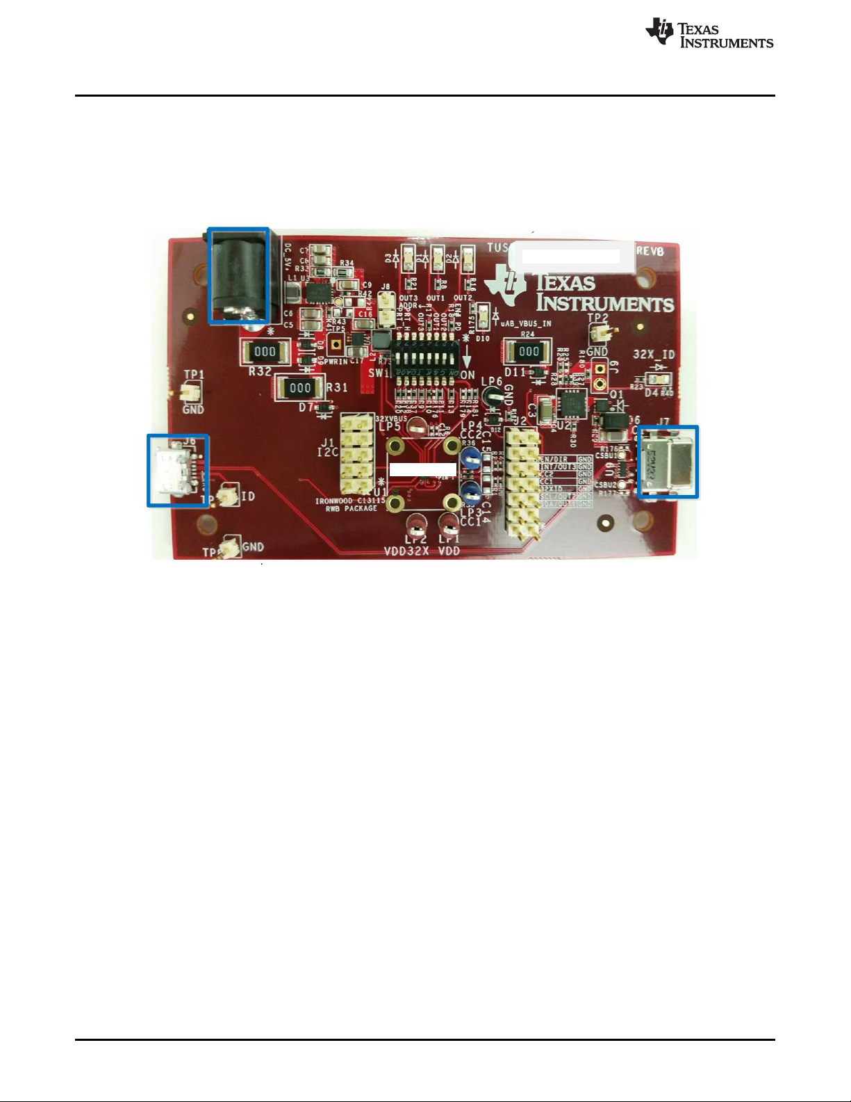
5 V DC IN
Type-C
Connector
uAB USB2
Connector
TUSB320-LA-EVM
TUSB320
What is the TUSB320-LA-EVM and TUSB320-HA-EVM?
1 What is the TUSB320-LA-EVM and TUSB320-HA-EVM?
The EVM is designed to evaluate TUSB320LA/HA devices. The EVM can be configured to operate in
DFP, UFP, or DRP mode via DIP switch selection and/or I2C control. All of the control inputs are also
selectable via DIP switch configuration. The TUSB320LA/HA devices can be used with legacy USB
systems or Type-C systems for evaluation purposes.
www.ti.com
2
TUSB320-LA-EVM and TUSB320-HA-EVM
Copyright © 2016–2018, Texas Instruments Incorporated
SLLU235A–January 2016–Revised November 2018
Submit Documentation Feedback
Page 3

www.ti.com
2 TUSB320-LA-EVM and TUSB320-HA-EVM Features
The EVM can be configured for the evaluation of DFP, UFP, or DRP Type-C implementation. The EVM
can also be configured to operate in I2C or GPIO mode. Default configuration is I2C.
This section describes EVM features enabling users to evaluate Type-C implementations in different
modes of operation.
2.1 Power
The EVM can be powered by USB VBUS or 5-V to 5.5-V DC IN through a power jack J5 (2-mm positive
tip, 6.5-mm negative outer shield). The VBUS can be provided via a legacy connection or Type-C
connection. When the EVM operates in DFP mode, the VBUS is provided through micro-AB connector J6,
if the board is connected to a USB host or VBUS source. When the EVM operates in UFP mode, the
VBUS is provided through Type-C connector J1, if the board is connected to a USB host or VBUS source
through a Type-C cable. The 5-V DC IN (J5) can also be used to supply power if a stand-alone operation
is desired without connecting to a USB VBUS power source. Due to diode/IR drop in the test setup, the
VBUS on the connector may be below the desired level. The board is designed to take up to 5.5 V
through DC_5V IN or TP5 (PWRIN) header for test purposes.
If D9 is installed on the board, do not connect the EVM to a USB Host system through the micro AB
USB2 connector(J6) at the same time 5 V is supplied through 5 V DC IN J5 or Type-C Connector J7.
Test loops and headers to power rails and GND are provided for test purposes. Some power rails can be
isolated from the main power supply by removing ferrite beads or passive components. Refer to the
schematics for power rail connection details. Do not supply external power through the test headers/loops
unless the power rail has been isolated from other power sources. In normal operation, power must be
provided through the USB connectors or DC power barrel only: J7, J6, or J5.
TUSB320-LA-EVM and TUSB320-HA-EVM Features
2.2 VBUS
2.2.1 VBUSOff time
To meet the VBUSOff time of 650 ms, remove the 10-µF capacitor C1. Current limiting can be reduced to
3 A–3.5 A by changing the R30 value to 47 kΩ.
2.2.2 VBUS Min Level
VBUS, provided on J1 or J6 may be lower than 4.75 V. For bus-powered devices to be attached to the
EVM for test purposes, TI recommends using a 5.5-V external power supply through J5 or TP5.
SLLU235A–January 2016–Revised November 2018
Submit Documentation Feedback
Copyright © 2016–2018, Texas Instruments Incorporated
TUSB320-LA-EVM and TUSB320-HA-EVM
3
Page 4
TUSB320-LA-EVM and TUSB320-HA-EVM Features
2.3 DIP Switch Setting
The DIP switch (SW1) is provided to configure the EVM in different modes of operation.
Table 1. DIP Switch Modes of Operation
www.ti.com
Reference
Designator
SW1.1 EN# for TUSB320LA
SW1.2 OUT2 OFF OUT2 = SCL with a pullup, if SW1.2 = OFF
SW1.3 OUT1 OFF OUT1 = SDA with a pullup, if SW1.2 = OFF
SW1.4 ADDR OFF For I2C mode of operation:
SW1.5 INT OFF INT = High, if SW1.5 = OFF
SW1.6 320_VBUS OFF 320_VBUS = high/low or open if option resistors are
SW1.7 PORT_H OFF PORT = Open, if SW1.7 = OFF
SW1.8 PORT_L ON PORT = Open, if SW1.8 = OFF
2.4 I2C
The I2C bus can be accessed through a header: J1 or J2. 4.7-kΩ pullups to 3.3 V are added on I2C SCL
and SDA. The ADDR pin can be pulled high or low through DIP SW configuration described in
Section 2.3, DIP Switch Setting. The ADDR pin determines the last bit of the TUSB320LA/HA I2C address
to be high or low. J1 is intended to match the Aardvark I2C programmer dongle pinout.
SW Control
Function
EN for TUSB320HA
Default
Switch Setting
ON for TUSB320LA
OFF for TUSB320HA
Description
EN# or EN = High, if SW1.1 = OFF
EN# or EN = Low, if SW1.1 = ON
OUT2 connected to LED, if SW1.2 = ON
OUT2 connected to LED, if SW1.2 = ON
ADDR = High, if SW1.4 = OFF
ADDR = Low, if SW1.4 = ON
For GPIO mode of operation:
Remove R12 and SW1.4 = OFF
INT = OUT3, if SW1.5 = ON
populated. Don’t care in normal operation.
PORT = High, if SW1.7 = ON
PORT = Low, if SW1.8 = ON
2.5 LEDs
Several LEDs are provided for easier debug purposes.
Reference Designator LED Name Description
D1 OUT1 Valid only in GPIO mode. Illuminates if OUT1 pin driven low.
D2 OUT2 Valid only in GPIO mode. Illuminates if OUT2 pin driven low.
D3 OUT3 Valid only in GPIO mode. Illuminates if OUT3 pin driven low.
D4 320 ID Illuminates if the ID pin of TUSB320LA/HA is driven low.
D10 POWER Illuminates if 5-V power is available.
Note that the OUT1, OUT2, OUT3 LEDs are used in GPIO mode of operation. The DIP SW must be
configured accordingly to configure the TUSB320-LA-EVM/TUSB320-HA-EVM in GPIO mode of operation.
The LED may light up dim even when OUT pins are not driven due to a pullup to 3.3 V.
4
TUSB320-LA-EVM and TUSB320-HA-EVM
Table 2. LEDs Debug Descriptions
SLLU235A–January 2016–Revised November 2018
Copyright © 2016–2018, Texas Instruments Incorporated
Submit Documentation Feedback
Page 5
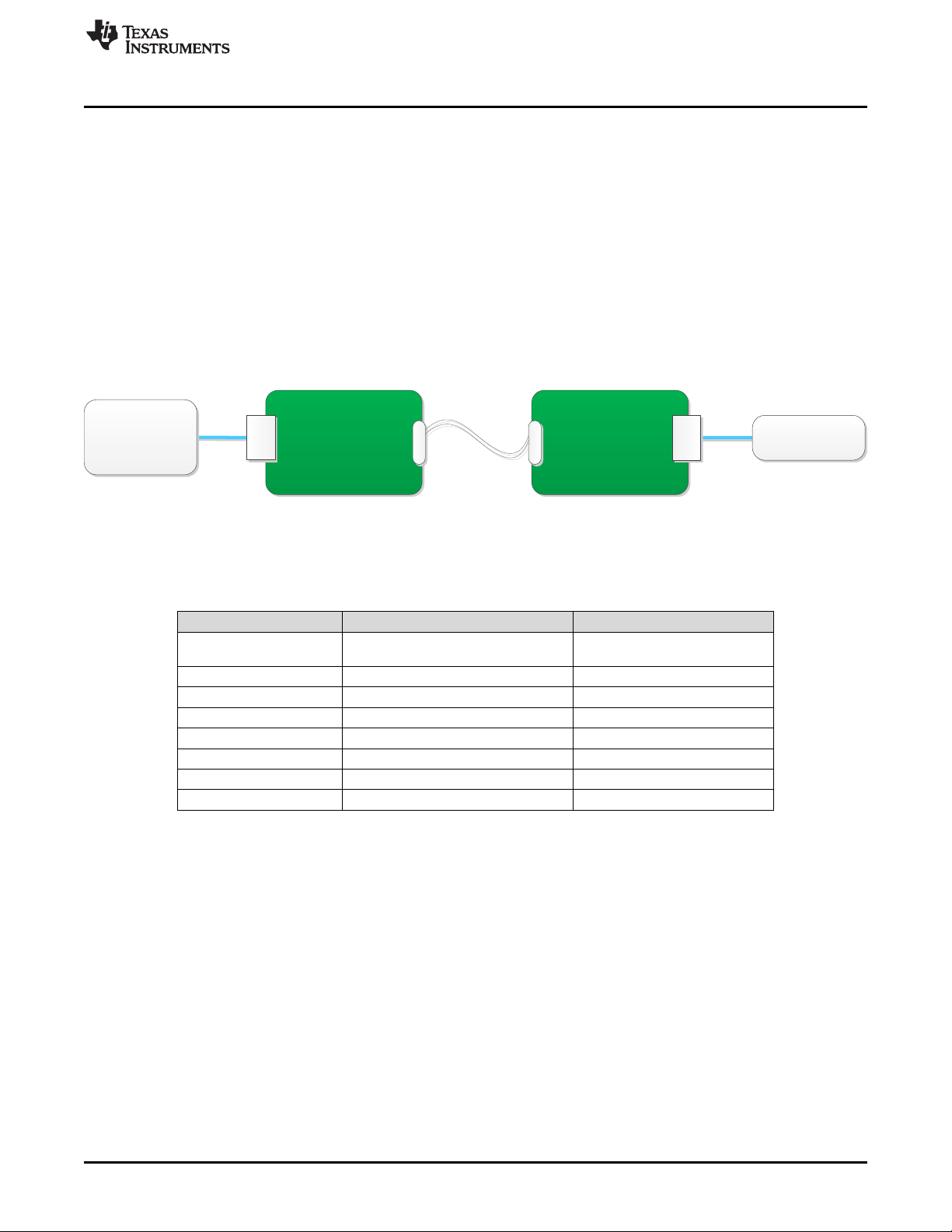
USB Host
Type C
USB
Type C
Micro
USB
USB Hub/Device
Configured as
UFP
Type-A to
micro-B
Cable
Micro AB to
Type-A
Receptacle
HD3SS2522 EVM
TUSB320-xA-EVM
www.ti.com
TUSB320-LA-EVM and TUSB320-HA-EVM Configuration Examples
3 TUSB320-LA-EVM and TUSB320-HA-EVM Configuration Examples
This section provides different configuration examples of the TUSB320-LA-EVM and TUSB320-HA-EVM:
DRP, DFP, or UFP operation. The PORT pins and the I2C must be programmed for the corresponding
mode of operation. No external 5-V DC IN is needed unless the board is to operate standalone without
any connections to the USB upstream or downstream port.
3.1 UFP Operation
The board can be configured to operate in UFP mode using the PORT pin on the board or I2C register
setting. If the PORT pin is to be used, SW1.8 must be switched ON and the Mode_Select bits at addr0x0A
bit 5:4 must be set to 00b. The Mode_Select is 00b by default, so there is no need to re-program unless it
has been reconfigured for other modes of operation.
Figure 1 describes an example configuration using HD3SS2522 and TUSB320-xA-EVM. The HD3SS2522
is a TI DFP CC controller, compliant to USB Type-C spec v1.1.
Figure 1. Example Configuration Using HD3SS2522 and TUSB320-xA-EVMs
1. TUSB320LA/HA UFP: Configure the DIP switches as shown in Table 3.
Table 3. TUSB320LA/HA UFP DIP Switch SW1 Settings
Reference Designator SW Control Function Switch Setting
SW1.1 EN#/EN ON for TUSB320LA
SW1.2 OUT2 OFF
SW1.3 OUT1 OFF
SW1.4 ADDR OFF
SW1.5 INT OFF
SW1.6 320_VBUS Don’t care
SW1.7 PORT_H OFF
SW1.8 PORT_L ON
OFF for TUSB320HA
2. Connect the HD3SS2522 EVM to a USB host.
3. Connect TUSB320LA/HA to the HD3SS2522 using a Type-C Cable. VBUS should be provided over
the Type-C cable connection. LED D10 should illuminate on the TUSB320LA/HA board. D3 and D4
should illuminate on the HD3S2522 indicating an UFP connection. Refer to the HD3SS2522 users
manual (SLLU215) for the details of the HD3SS2522 EVM operation.
4. USB devices plugged into the Micro AB USB receptacle (J6) of the TUSB320LA/HA UFP EVM should
enumerate at USB2 speed: HS, FS, or LS.
SLLU235A–January 2016–Revised November 2018
Submit Documentation Feedback
Copyright © 2016–2018, Texas Instruments Incorporated
TUSB320-LA-EVM and TUSB320-HA-EVM
5
Page 6
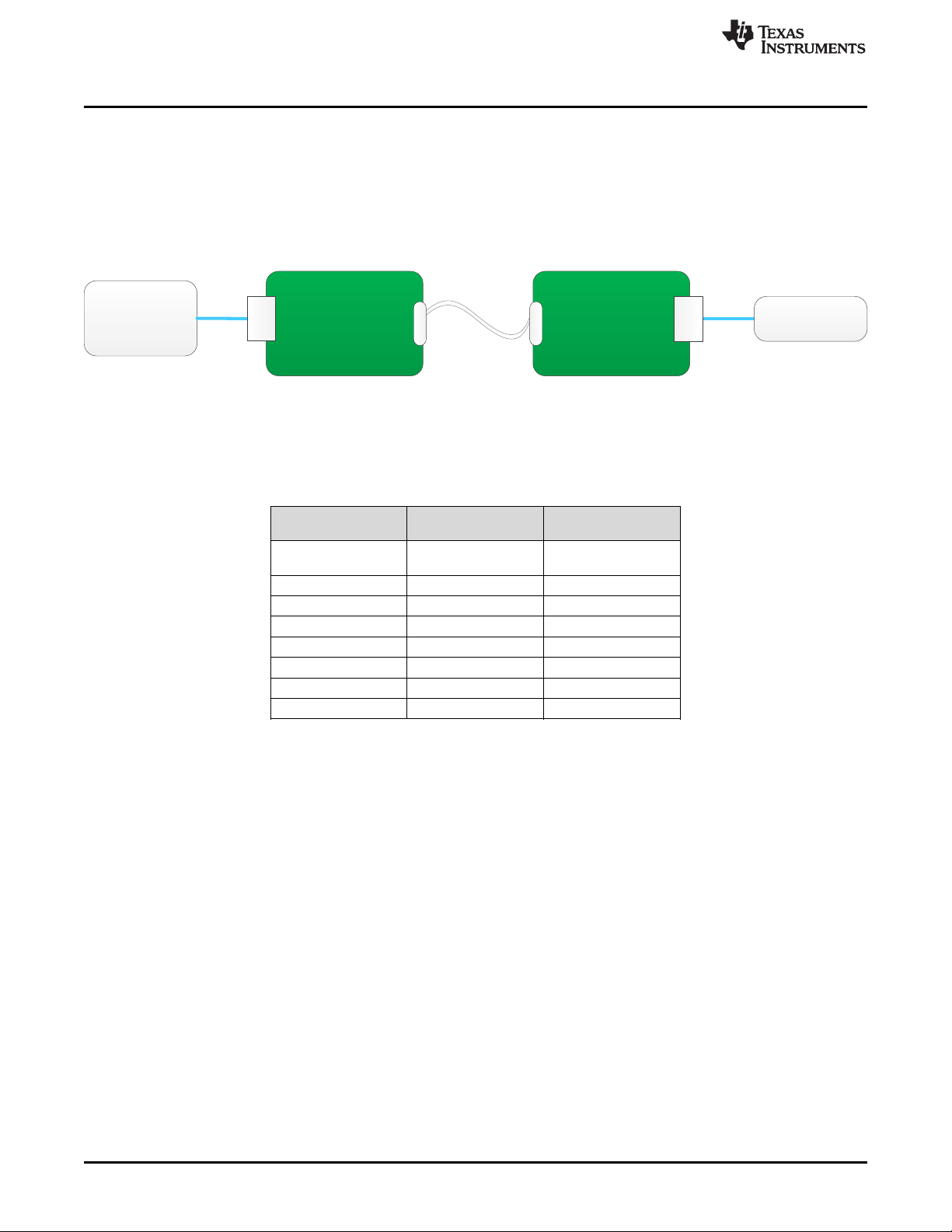
Type-A to
micro-B
Cable
USB Host
Type C
TUSB320-xA-EVM
Micro
USB
Type C
TUSB320-xA-EVM
Micro
USB
USB Hub/Device
Configured as
UFP
Micro AB to
Type A
Receptacle
Configured as
DFP
TUSB320-LA-EVM and TUSB320-HA-EVM Configuration Examples
3.2 DFP Operation
The board can be configured to operate in DFP mode using the PORT pin on the board or I2C register
setting. If the PORT pin is used, SW1.7 must be switched ON and the Mode_Select bits at addr0x0A bit
5:4 must be set to 00b. The Mode_Select is 00b by default, so there is no need to reprogram unless it has
been reconfigured for other modes of operation.
Figure 2 describes an example configuration using two TUSB320-xA-EVMs: one configured as DFP, the
other configured as UFP. Refer to Section 3.1 for TUSB320LA/HA UFP EVM configuration.
Figure 2. Example Configuration Using Two TUSB320-xA-EVMs
1. Configure TUSB320LA/HA DFP EVM DIP switch SW1 as shown in Table 4.
Table 4. TUSB320LA/HA DFP EVM DIP Switch SW1
Configuration
www.ti.com
Reference
Designator
SW1.1 EN#/EN ON for TUSB320LA
SW1.2 OUT2 OFF
SW1.3 OUT1 OFF
SW1.4 ADDR OFF
SW1.5 INT OFF
SW1.6 320_VBUS Don’t care
SW1.7 PORT_H ON
SW1.8 PORT_L OFF
SW Control Function Switch Setting
OFF for TUSB320HA
2. Connect TUSB320LA/HA DFP EVM to a legacy USB host using a Type-A to micro-B cable via microAB connector (J5) provided on board. The LED D10 should illuminate by the VBUS provided by the
legacy USB host over the Type-A to micro-B cable connection.
3. Connect TUSB320LA/HA UFP EVM to the TUSB320LA/HA DFP EVM using a Type-C Cable. The
TUSB320LA/HA UFP EVM should be powered by VBUS provided over the Type-C cable connection.
The LED D10 on the TUSB320LA/HA UFP EVM should also light up. Upon the Type-C cable, attach to
the TUSB320LA/HA DFP EVM, D4 should light up indicating the ID pin has been driven low from the
TUSB320LA/HA.
4. The USB device plugged into the micro-AB USB receptacle (J6) of the TUSB320LA/HA UFP EVM
should enumerate at USB2 speed: HS, FS, or LS.
6
TUSB320-LA-EVM and TUSB320-HA-EVM
Copyright © 2016–2018, Texas Instruments Incorporated
SLLU235A–January 2016–Revised November 2018
Submit Documentation Feedback
Page 7

USB Host
Type C
USB
Type C
Micro
USB
USB Hub/Device
Configured as
DRP
Micro AB to
Type-A
Receptacle
HD3SS2522 EVM
TUSB320-xA-EVM
www.ti.com
3.3 DRP Operation
The board can be configured to operate in DFP mode using the PORT pin on the board or I2C register
setting. If the PORT pin is used, SW1.7 must be switched ON and the Mode_Select bits at addr0x0A bit
5:4 must be set to 00b. The Mode_Select is 00b by default, so there is no need to reprogram unless it has
been reconfigured for other modes of operation. It is important that both SW settings are in the OFF
position to have the PORT input to the TUSB320LA/HA open.
Figure 3 illustrates an example configuration using HD3SS2522 and TUSB320-xA-EVMs. The
HD3SS2522 is a TI DFP CC controller, compliant to USB Type-C spec v1.1.
Figure 3. Example Configuration Using HD3SS2522 and TUSB320-xA-EVMs
1. Configure the TUSB320LA/HA DRP EVM DIP switch SW1 as shown in Table 5.
TUSB320-LA-EVM and TUSB320-HA-EVM Configuration Examples
Table 5. TUSB320LA/HA DRP EVM DIP Switch SW1
Reference
Designator
SW1.1 EN#/EN ON for TUSB320LA
SW1.2 OUT2 OFF
SW1.3 OUT1 OFF
SW1.4 ADDR OFF
SW1.5 INT OFF
SW1.6 320_VBUS Don’t care
SW1.7 PORT_H OFF
SW1.8 PORT_L OFF
SW Control Function Switch Setting
OFF for TUSB320HA
2. Connect the HD3SS2522 EVM to a USB host.
3. Connect the TUSB320LA/HA to the HD3SS2522 using a Type-C cable. VBUS should be provided over
the Type-C cable connection. LED D10 should light up on the TUSB320LA/HA board. D3 and D4
should light up on the HD3S2522 indicating an UFP connection. Refer to the HD3SS2522 users
manual (SLLU215) for details on the HD3SS2522 EVM operation.
4. The USB devices plugged into the micro-AB USB receptacle (J6) of the TUSB320LA/HA UFP EVM
should enumerate at USB2 speed: HS, FS, or LS.
SLLU235A–January 2016–Revised November 2018
Submit Documentation Feedback
Copyright © 2016–2018, Texas Instruments Incorporated
TUSB320-LA-EVM and TUSB320-HA-EVM
7
Page 8
Type-A to
micro-B
Cable
USB Host
Type C
Micro
USB
Type C
Micro
USB
USB Hub/Device
Configured as
UFP
Micro AB
to Type-A
Receptacle
Configured as
DRP
TUSB320-xA-EVM TUSB320-xA-EVM
TUSB320-LA-EVM and TUSB320-HA-EVM Configuration Examples
Figure 4 describes an example configuration using two TUSB320-xA-EVMs: one configured as DRP, the
other configured as UFP. Refer to Section 3.1 for TUSB320LA/HA UFP EVM configuration.
Figure 4. Example Configuration Using Two TUSB320-xA-EVMs
1. Configure the TUSB320LA/HA DRP DIP switch SW1 as shown in Table 6.
Table 6. TUSB320LA/HA DRP DIP Switch SW1
Configuration
www.ti.com
Reference
Designator
SW1.1 EN#/EN ON for TUSB320LA
SW1.2 OUT2 OFF
SW1.3 OUT1 OFF
SW1.4 ADDR OFF
SW1.5 INT OFF
SW1.6 320_VBUS Don’t care
SW1.7 PORT_H OFF
SW1.8 PORT_L OFF
SW Control Function Switch Setting
OFF for TUSB320HA
2. Connect the TUSB320LA/HA DRP EVM to a legacy USB host using a Type-A to micro-B cable via
micro-AB connector (J5) provided on the board. The LEDs D1, D2, and D3 should be lit up by the
VBUS provided by the legacy USB host over the Type-A to micro-B cable connection.
3. Connect the TUSB320LA/HA UFP EVM to the TUSB320LA/HA DFP EVM using a Type-C cable. The
TUSB320LA/HA UFP EVM should be powered by VBUS provided over the Type-C cable connection.
The LED D10 on the TUSB320LA/HA UFP EVM should also light up. Upon the Type-C cable attached
to the TUSB320LA/HA DFP EVM, D4 should light up indicating the ID pin has been driven low from the
TUSB320LA/HA.
4. The USB device plugged into the micro-AB USB receptacle (J6) of the TUSB320LA/HA UFP EVM
should enumerate at USB2 speed: HS, FS, or LS.
NOTE: Two TUSB320-xA-EVMs can be used for DRP to DRP connection. In this configuration, it is
not recommended to connect the EVM to legacy USB systems as the role cannot be
predicted until both sides enter the attach state. This configuration can be used for
evaluation purposes with 5 V provided via DC IN (J5) on both boards. One of the
TUSB320HA EVMs can be configured to be a preferred SRC or SNK by enabling the
TRY.SRC or TRY.SNK feature via I2C access. Refer to the device datasheet for details on
how to enable this feature.
8
TUSB320-LA-EVM and TUSB320-HA-EVM
Copyright © 2016–2018, Texas Instruments Incorporated
SLLU235A–January 2016–Revised November 2018
Submit Documentation Feedback
Page 9

CC1
CC2
TypeC_VBUS
VBUS SW
ID
VBUS_DET
CC1
CC2
Type C
Receptacl e
micro AB
Receptacl e
D+
D-
uAB_VBUS
DC_IN
DC IN
Test Header/
Switch
EN#
ADDR
PORT
OUT[1,2,3]
TUSB320LA
Vdd
VDD_320
VDD_320
PWR_IN
PWR_IN
TPS630 20
TPS259 10
4.5V-5 .5V
www.ti.com
4 EVM Schematics
4.1 TUSB320-LA-EVM Schematics
Figure 5, Figure 6, and Figure 7 illustrate the TUSB320-LA-EVM revision B schematics.
EVM Schematics
SLLU235A–January 2016–Revised November 2018
Submit Documentation Feedback
Figure 5. TUSB320-LA-EVM Schematic
Copyright © 2016–2018, Texas Instruments Incorporated
TUSB320-LA-EVM and TUSB320-HA-EVM
9
Page 10

SilkScreen: I2C
SILKSCREENGND
GND
SILKSCREEN
SilkScreen: TestPoint
SilkScreen:
GND
SilkScreen:
SDA/OUT1
SCL/OUT2
INT/OUT3
CC1
CC2
32xID
EN_DIR
OUT1
SilkScreen:
OUT2SilkScreen:
OUT3SilkScreen:
32xIDSilkScreen:
NOTE: ALLDIFF PAIRS ARE
ROUTED 85 TO 90 OHMS
DIFFERENTIALAND 50 OHMS
COMMON MODE. ALL OTHER
TRACES ARE 50 OHM.
LEDs
Test Header
microAB Receptacle
SilkScreen:
EN#
ADDR
OUT1
OUT2
OUT3
PORTH
PORTL
DIP Switches
Type C Connector
SilkScreen: CSBU1
CSBU2
SilkScreen:
TypeC Connector Pin Mapping
B8
B7
B6
B5
B4
B3
B2
B1
DN2
VBUS
GND
SBU2
B12
B11
CC1
B10
DP1
GND
DN1
SSTXP1
VBUS
SBU1
SSTXN2
SSTXN1
SSTXP2
SSRXP1
SSRXP2
SSRXN1
SSRXN2
SSTXP1
SSTXP2
DP2
SSTXN1
SSTXN2
CC2
VBUS
GND
A1
A2
A3
A4
A5
A6
A7
A8
A9
GND
VBUS
A10
A11
SSRXP1
A12
SSRXN1
SSRXP2
SSRXN1
B9
STUB on DP or DN
no greater than
3.5mm
Test
Purposes
Only
TUSB320HA
Max Value 220uF
SilkScreen:
VDD VDD32x
SilkScreen:
SilkScreen:
CC1
SilkScreen:
CC2
NOTE: Place LP1, LP2, LP3, LP4 and LP5 5mm away from U1 socket outline
32xVBUS
SilkScreen:
GND
SilkScreen:
I2C
Recommended for ESD protection.
ADDR=L: DNI R10, Install R176
ADDR=H: Install R10, DNI R176
TUSB320HA Default
32xVBUS
VBUS detection option for EN
SCL_OUT2
SDA_OUT1
USB2_P0
USB2_N0
CC1
CC2
SDA_OUT1
SCL_OUT2
OUT1
OUT1_RED
OUT2
OUT2_RED
OUT3
OUT3_RED
ID_RED 320_ID320_ID_D
PORT
PORT_L
PORT_H
SCL_OUT2
EN#_SW EN#_PD
SDA_OUT1
ADDR
INT_OUT3
OUT1
OUT3
320_VBUS_L
CC1
CC2
CSBU1
CSBU2
USB2_P0
USB2_N0
CSBU1
CSBU2
INT_OUT3
CC1
CC2
CC1_R
CC2_R
ADDR
SCL_OUT2
SDA_OUT1
PORT
320_VBUS
OUT2
GPIO_MD
320_ID
INT_OUT3
microAB_ID
320_ID
USB2_P0
USB2_N0
CC2
CC1
CC2
CC1
USB2_P0
USB2_N0
320_VBUS
EN#_SW
EN#
microAB_ID
EN#
EN#
micAB_VBUS
VDD_320
VDD_320
VDD_320
VDD_320
VDD_320
VDD_320
VDD_320
TypeC_VBUS
VDD320_LPVDD_320 TypeC_VBUS
VDD_3P3V
TypeC_VBUS
320_ID pg3
R8 500R
R9
200K
J2
HEADER 7X2 0.1" thru-hole
2
4
6
8
10
12
14
1
3
5
7
9
11
13
D12
NC, RB751V-40
1 2
C14
NC, 10uF
D4
LED Red 0805
D1
LED Red 0805
R3
NC
C15
NC, 10uF
R38
NC, 100K
R13
4.7K
R178
NC
R176
NC
C2
10uF
J6
USB2_micAB_Recept
VBUS
1
D-
2
D+
3
ID
4
GND
5
Shield1
6
Shield2
7
Shield3
8
Shield4
9
Shield5
10
Shield6
11
TP3
15-mil TEST PAD
1
R12
100K
R37
NC, 1M +/-1%
R1
NC
C1
NC, 10uF
C12
NC, 1nF
R4
NC
C11
0.1uF
R182 1M +/-1%
TP4
15-mil TEST PAD
1
R14
NC, 100K
R2
NC
R181 0
R11
4.7K
R23 500R
R16 500R
SW1
8-POS 50-MIL SMT
TDA08H0SK1R
C&K (ITT-CANNON)
1
2
3
4
5
6
7
8
16
15
14
13
12
11
10
9
LP5
TP7
0.1" Test Post
1
R5 NC, 0
LP6
R20
4.7K
U1
TUSB320HA
CC1
1
CC2
2
PORT
3
VBUS_DET
4
ADDR
5
INT#/OUT3
6
SDA/OUT1
7
SCL/OUT28ID
9
GND
10
EN
11
VDD
12
R18
1K
U9
TPD4E05U06
D1+
1
D1-
2
GND
3
D2+
4
D2-5NC6
6
NC7
7
GND1
8
NC9
9
NC10
10
R10
100K
R6 1M +/-1%
FB1
220 @ 100MHZ
R40 0
TP8
0.1" Test Post
1
LP2
TP1
0.1" Test Post
1
J1
Header 5x2 0.1" thru-hole
2
4
6
8
10
1
3
5
7
9
R35 0
J7
USB_TypeC_Receptacle_Topmount
GND0
A1
SSTXP1
A2
SSTXN1
A3
VBUS1
A4
CC1
A5
DP1
A6
DN1
A7
SBU1
A8
VBUS2
A9
SSRXN2
A10
SSRXP2
A11
GND1
A12
GND2
B1
SSTXP2
B2
SSTXN2
B3
VBUS3
B4
CC2
B5
DP2
B6
DN2
B7
SBU2
B8
VBUS4
B9
SSRXN1
B10
SSRXP1
B11
GND3
B12
Shield1
G1
Shield2
G2
Shield3
G3
Shield4
G4
Shield5
G5
Shield6
G6
D2
LED Red 0805
LP3
R179
100K
TP2
0.1" Test Post
1
LP1
LP4
R36 0
R21 500R
R17
1K
R177
NC
D3
LED Red 0805
EVM Schematics
www.ti.com
10
TUSB320-LA-EVM and TUSB320-HA-EVM
Figure 6. TUSB320-LA-EVM Components
Copyright © 2016–2018, Texas Instruments Incorporated
SLLU235A–January 2016–Revised November 2018
Submit Documentation Feedback
Page 11
uABVBUS_IN
VIN = 4.5-5.5V Vout = 4.25V
5V DC Input
External power
supply option for
test purp oses only
Connection to
TypeC_VBUS,
micAB_VBUS and
DC_IN must be
removed by
uninstalling 0-Ohm
resis tors
SilkScreen:
MAYNEED TO CHANGE TO HIGHER POWER REGULATOR
SilkScreen:
PWRIN
NOTE: POPULATE JUMPER BY DEFAULT
TUSB320
Vout = 5V
R33 = 1.5M
R34 = 200K
R33 = 1.8M
R34 = 200K
DNI J9
25910FLT#
25910_ILIM1
TPS25910_GATE1
TPS25910_GATE1
micAB_VBUS_IN
63020_L2
63020_L1 63020_VINA
63020_FB
TypeC_VBUS_R
DC_IN_R DC_IN
63020_PG
25910EN#
63020_PS
63020_EN
63020_PS
63020_EN
micABVBUS_OUT
micAB_VBUS
TypeC_VBUS
PWR_IN
PWR_IN
PWR_IN
PWR_IN
micAB_VBUS
TypeC_VBUS
PWR_IN
VDD_320
VDD_320
VDD_320
PWR_IN
VDD_3P3V
320_IDpg2
R41 0
U4
TPS62082DSGT
VIN
8
EN
1
MODE
3
GND
2
PwPd
9
FB
4
VOS
5
SW
7
PG
6
C6
10uF
R28
NC, 10K
D8
RB751V-40
1
2
TP6
15-mil TEST PAD
1
R29
1M
R24
0R 3A
C5
10uF
L1
1.0uH(0.06Ohm)
D9
DNI, RB751V-40
1
2
R180
0
J5
DC_POWER_JACK
1
2
3
C16
10uF
CSD17313Q2
Q1
3
2
1
6
4
8
7
5
D6
SMAJ20A
R73 174K
C9
100nF
J9
1
2
D7
RB751V-40
12
R34
200K
D10
LED Green 0805
R43
NC,10K
R33
1.5M
R175
330
0402
5%
R32
0R 3A
C7
22uF
U2
TPS25910RSA
EN#
16
FLT#
15
OUT1
10
OUT2
11
OUT3
12
GND1
14
GND2
13
GND3
9
IN1
1
IN2
2
IN3
3
GATE
4
GND4
5
GND5
6
GND6
8
ILIM
7
PWPD
17
L2
1uH
U3
TPS63020
VINA
1
GND
2
FB
3
VOUT_1
4
VOUT_2
5
L2_1
6
L2_2
7
L1_1
8
L1_2
9
VIN_1
10
VIN_2
11
EN
12
PS/SYNC
13
PG
14
PAD
15
R44
NC, 10K
TP5
NC, 0.1mil Test Post
1
R31
0R 3A
C3
47uF
D11
RB751V-40
1
2
R26
200K
R39
0
R27
10K
C17
22uF
R25
NC, 10K
C8
22uF
C4
47nF
R42
0
R30
47K
J8
1
2
www.ti.com
EVM Schematics
Figure 7. TUSB320-LA-EVM Power
Copyright © 2016–2018, Texas Instruments Incorporated
SLLU235A–January 2016–Revised November 2018
Submit Documentation Feedback
TUSB320-LA-EVM and TUSB320-HA-EVM
11
Page 12

CC1
CC2
TypeC_VBUS
VBUS SW
ID
VBUS_DET
CC1
CC2
Type C
Receptacl e
micro AB
Receptacl e
D+
D-
uAB_VBUS
DC_IN
DC IN
Test Header/
Switch
EN
ADDR
PORT
OUT[1,2,3]
TUSB320HA
Vdd
VDD_320
VDD_320
PWR_IN
PWR_IN
TPS630 20
TPS259 10
4.5V-5 .5V
EVM Schematics
4.2 TUSB320-HA-EVM Schematics
Figure 8, Figure 9, and Figure 10 illustrate the TUSB320-HA-EVM revision B schematics.
www.ti.com
12
TUSB320-LA-EVM and TUSB320-HA-EVM
Figure 8. TUSB320-HA-EVM Schematic
Copyright © 2016–2018, Texas Instruments Incorporated
SLLU235A–January 2016–Revised November 2018
Submit Documentation Feedback
Page 13

SilkScreen: I2C
SILKSCREENGND
GND
SILKSCREEN
SilkScreen: TestPoint
SilkScreen:
GND
SilkScreen:
SDA/OUT1
SCL/OUT2
INT/OUT3
CC1
CC2
32xID
EN_DIR
OUT1
SilkScreen:
OUT2SilkScreen:
OUT3SilkScreen:
32xIDSilkScreen:
NOTE: ALLDIFF PAIRS ARE
ROUTED 85 TO 90 OHMS
DIFFERENTIALAND 50 OHMS
COMMON MODE. ALL OTHER
TRACES ARE 50 OHM.
LEDs
Test Header
microAB Receptacle
SilkScreen:
EN#
ADDR
OUT1
OUT2
OUT3
PORTH
PORTL
DIP Switches
Type C Connector
SilkScreen: CSBU1
CSBU2
SilkScreen:
TypeC Connector Pin Mapping
B8
B7
B6
B5
B4
B3
B2
B1
DN2
VBUS
GND
SBU2
B12
B11
CC1
B10
DP1
GND
DN1
SSTXP1
VBUS
SBU1
SSTXN2
SSTXN1
SSTXP2
SSRXP1
SSRXP2
SSRXN1
SSRXN2
SSTXP1
SSTXP2
DP2
SSTXN1
SSTXN2
CC2
VBUS
GND
A1
A2
A3
A4
A5
A6
A7
A8
A9
GND
VBUS
A10
A11
SSRXP1
A12
SSRXN1
SSRXP2
SSRXN1
B9
STUB on DP or DN
no greater than
3.5mm
Test
Purposes
Only
TUSB320HA
Max Value 220uF
SilkScreen:
VDD VDD32x
SilkScreen:
SilkScreen:
CC1
SilkScreen:
CC2
NOTE: Place LP1, LP2, LP3, LP4 and LP5 5mm away from U1 socket outline
32xVBUS
SilkScreen:
GND
SilkScreen:
I2C
Recommended for ESD protection.
ADDR=L: DNI R10, Install R176
ADDR=H: Install R10, DNI R176
TUSB320HA Default
32xVBUS
VBUS detection option for EN
SCL_OUT2
SDA_OUT1
USB2_P0
USB2_N0
CC1
CC2
SDA_OUT1
SCL_OUT2
OUT1
OUT1_RED
OUT2
OUT2_RED
OUT3
OUT3_RED
ID_RED 320_ID320_ID_D
PORT
PORT_L
PORT_H
SCL_OUT2
EN#_SW EN#_PD
SDA_OUT1
ADDR
INT_OUT3
OUT1
OUT3
320_VBUS_L
CC1
CC2
CSBU1
CSBU2
USB2_P0
USB2_N0
CSBU1
CSBU2
INT_OUT3
CC1
CC2
CC1_R
CC2_R
ADDR
SCL_OUT2
SDA_OUT1
PORT
320_VBUS
OUT2
GPIO_MD
320_ID
INT_OUT3
microAB_ID
320_ID
USB2_P0
USB2_N0
CC2
CC1
CC2
CC1
USB2_P0
USB2_N0
320_VBUS
EN#_SW
EN#
microAB_ID
EN#
EN#
micAB_VBUS
VDD_320
VDD_320
VDD_320
VDD_320
VDD_320
VDD_320
VDD_320
TypeC_VBUS
VDD320_LPVDD_320 TypeC_VBUS
VDD_3P3V
TypeC_VBUS
320_ID pg3
R8 500R
R9
200K
J2
HEADER 7X2 0.1" thru-hole
2
4
6
8
10
12
14
1
3
5
7
9
11
13
D12
NC, RB751V-40
1 2
C14
NC, 10uF
D4
LED Red 0805
D1
LED Red 0805
R3
NC
C15
NC, 10uF
R38
NC, 100K
R13
4.7K
R178
NC
R176
NC
C2
10uF
J6
USB2_micAB_Recept
VBUS
1
D-
2
D+
3
ID
4
GND
5
Shield1
6
Shield2
7
Shield3
8
Shield4
9
Shield5
10
Shield6
11
TP3
15-mil TEST PAD
1
R12
100K
R37
NC, 1M +/-1%
R1
NC
C1
NC, 10uF
C12
NC, 1nF
R4
NC
C11
0.1uF
R182 1M +/-1%
TP4
15-mil TEST PAD
1
R14
NC, 100K
R2
NC
R181 0
R11
4.7K
R23 500R
R16 500R
SW1
8-POS 50-MIL SMT
TDA08H0SK1R
C&K (ITT-CANNON)
1
2
3
4
5
6
7
8
16
15
14
13
12
11
10
9
LP5
TP7
0.1" Test Post
1
R5 NC, 0
LP6
R20
4.7K
U1
TUSB320HA
CC1
1
CC2
2
PORT
3
VBUS_DET
4
ADDR
5
INT#/OUT3
6
SDA/OUT1
7
SCL/OUT28ID
9
GND
10
EN
11
VDD
12
R18
1K
U9
TPD4E05U06
D1+
1
D1-
2
GND
3
D2+
4
D2-5NC6
6
NC7
7
GND1
8
NC9
9
NC10
10
R10
100K
R6 1M +/-1%
FB1
220 @ 100MHZ
R40 0
TP8
0.1" Test Post
1
LP2
TP1
0.1" Test Post
1
J1
Header 5x2 0.1" thru-hole
2
4
6
8
10
1
3
5
7
9
R35 0
J7
USB_TypeC_Receptacle_Topmount
GND0
A1
SSTXP1
A2
SSTXN1
A3
VBUS1
A4
CC1
A5
DP1
A6
DN1
A7
SBU1
A8
VBUS2
A9
SSRXN2
A10
SSRXP2
A11
GND1
A12
GND2
B1
SSTXP2
B2
SSTXN2
B3
VBUS3
B4
CC2
B5
DP2
B6
DN2
B7
SBU2
B8
VBUS4
B9
SSRXN1
B10
SSRXP1
B11
GND3
B12
Shield1
G1
Shield2
G2
Shield3
G3
Shield4
G4
Shield5
G5
Shield6
G6
D2
LED Red 0805
LP3
R179
100K
TP2
0.1" Test Post
1
LP1
LP4
R36 0
R21 500R
R17
1K
R177
NC
D3
LED Red 0805
www.ti.com
EVM Schematics
SLLU235A–January 2016–Revised November 2018
Submit Documentation Feedback
Figure 9. TUSB320-HA-EVM Components
Copyright © 2016–2018, Texas Instruments Incorporated
TUSB320-LA-EVM and TUSB320-HA-EVM
13
Page 14
uABVBUS_IN
VIN = 4.5-5.5V Vout = 4.25V
5V DC Input
External power
supply option for
test purp oses only
Connection to
TypeC_VBUS,
micAB_VBUS and
DC_IN must be
removed by
uninstalling 0-Ohm
resis tors
SilkScreen:
MAYNEED TO CHANGE TO HIGHER POWER REGULATOR
SilkScreen:
PWRIN
NOTE: POPULATE JUMPER BY DEFAULT
TUSB320HA
Vout = 5V
R33 = 1.5M
R34 = 200K
R33 = 1.8M
R34 = 200K
DNI J9
25910FLT#
25910_ILIM1
TPS25910_GATE1
TPS25910_GATE1
micAB_VBUS_IN
63020_L2
63020_L1 63020_VINA
63020_FB
TypeC_VBUS_R
DC_IN_R DC_IN
63020_PG
25910EN#
63020_PS
63020_EN
63020_PS
63020_EN
micABVBUS_OUT
micAB_VBUS
TypeC_VBUS
PWR_IN
PWR_IN
PWR_IN
PWR_IN
micAB_VBUS
TypeC_VBUS
PWR_IN
VDD_320
VDD_320
VDD_320
PWR_IN
VDD_3P3V
320_IDpg2
R41 0
U4
TPS62082DSGT
VIN
8
EN
1
MODE
3
GND
2
PwPd
9
FB
4
VOS
5
SW
7
PG
6
C6
10uF
R28
NC, 10K
D8
RB751V-40
1
2
TP6
15-mil TEST PAD
1
R29
1M
R24
0R 3A
C5
10uF
L1
1.0uH(0.06Ohm)
D9
DNI, RB751V-40
1
2
R180
0
J5
DC_POWER_JACK
1
2
3
C16
10uF
CSD17313Q2
Q1
3
2
1
6
4
8
7
5
D6
SMAJ20A
R73 174K
C9
100nF
J9
1
2
D7
RB751V-40
12
R34
200K
D10
LED Green 0805
R43
NC,10K
R33
1.5M
R175
330
0402
5%
R32
0R 3A
C7
22uF
U2
TPS25910RSA
EN#
16
FLT#
15
OUT1
10
OUT2
11
OUT3
12
GND1
14
GND2
13
GND3
9
IN1
1
IN2
2
IN3
3
GATE
4
GND4
5
GND5
6
GND6
8
ILIM
7
PWPD
17
L2
1uH
U3
TPS63020
VINA
1
GND
2
FB
3
VOUT_1
4
VOUT_2
5
L2_1
6
L2_2
7
L1_1
8
L1_2
9
VIN_1
10
VIN_2
11
EN
12
PS/SYNC
13
PG
14
PAD
15
R44
NC, 10K
TP5
NC, 0.1mil Test Post
1
R31
0R 3A
C3
47uF
D11
RB751V-40
1
2
R26
200K
R39
0
R27
10K
C17
22uF
R25
NC, 10K
C8
22uF
C4
47nF
R42
0
R30
47K
J8
1
2
EVM Schematics
www.ti.com
Figure 10. TUSB320-HA-EVM Power
Copyright © 2016–2018, Texas Instruments Incorporated
14
TUSB320-LA-EVM and TUSB320-HA-EVM
SLLU235A–January 2016–Revised November 2018
Submit Documentation Feedback
Page 15

www.ti.com
Revision History
Revision History
NOTE: Page numbers for previous revisions may differ from page numbers in the current version.
Changes from Original (january 2016) to A Revision ..................................................................................................... Page
• Changed TUSB321 To TUSB320 throughout the document........................................................................ 2
• Changed pin VBUS To: VBUS_DET in Figure 5 and Figure 6...................................................................... 9
• Changed pin VBUS To: VBUS_DET in Figure 8 and Figure 9 .................................................................... 12
SLLU235A–January 2016–Revised November 2018
Submit Documentation Feedback
Copyright © 2016–2018, Texas Instruments Incorporated
Revision History
15
Page 16

STANDARD TERMS FOR EVALUATION MODULES
1. Delivery: TI delivers TI evaluation boards, kits, or modules, including any accompanying demonstration software, components, and/or
documentation which may be provided together or separately (collectively, an “EVM” or “EVMs”) to the User (“User”) in accordance
with the terms set forth herein. User's acceptance of the EVM is expressly subject to the following terms.
1.1 EVMs are intended solely for product or software developers for use in a research and development setting to facilitate feasibility
evaluation, experimentation, or scientific analysis of TI semiconductors products. EVMs have no direct function and are not
finished products. EVMs shall not be directly or indirectly assembled as a part or subassembly in any finished product. For
clarification, any software or software tools provided with the EVM (“Software”) shall not be subject to the terms and conditions
set forth herein but rather shall be subject to the applicable terms that accompany such Software
1.2 EVMs are not intended for consumer or household use. EVMs may not be sold, sublicensed, leased, rented, loaned, assigned,
or otherwise distributed for commercial purposes by Users, in whole or in part, or used in any finished product or production
system.
2 Limited Warranty and Related Remedies/Disclaimers:
2.1 These terms do not apply to Software. The warranty, if any, for Software is covered in the applicable Software License
Agreement.
2.2 TI warrants that the TI EVM will conform to TI's published specifications for ninety (90) days after the date TI delivers such EVM
to User. Notwithstanding the foregoing, TI shall not be liable for a nonconforming EVM if (a) the nonconformity was caused by
neglect, misuse or mistreatment by an entity other than TI, including improper installation or testing, or for any EVMs that have
been altered or modified in any way by an entity other than TI, (b) the nonconformity resulted from User's design, specifications
or instructions for such EVMs or improper system design, or (c) User has not paid on time. Testing and other quality control
techniques are used to the extent TI deems necessary. TI does not test all parameters of each EVM.
User's claims against TI under this Section 2 are void if User fails to notify TI of any apparent defects in the EVMs within ten (10)
business days after delivery, or of any hidden defects with ten (10) business days after the defect has been detected.
2.3 TI's sole liability shall be at its option to repair or replace EVMs that fail to conform to the warranty set forth above, or credit
User's account for such EVM. TI's liability under this warranty shall be limited to EVMs that are returned during the warranty
period to the address designated by TI and that are determined by TI not to conform to such warranty. If TI elects to repair or
replace such EVM, TI shall have a reasonable time to repair such EVM or provide replacements. Repaired EVMs shall be
warranted for the remainder of the original warranty period. Replaced EVMs shall be warranted for a new full ninety (90) day
warranty period.
3 Regulatory Notices:
3.1 United States
3.1.1 Notice applicable to EVMs not FCC-Approved:
FCC NOTICE: This kit is designed to allow product developers to evaluate electronic components, circuitry, or software
associated with the kit to determine whether to incorporate such items in a finished product and software developers to write
software applications for use with the end product. This kit is not a finished product and when assembled may not be resold or
otherwise marketed unless all required FCC equipment authorizations are first obtained. Operation is subject to the condition
that this product not cause harmful interference to licensed radio stations and that this product accept harmful interference.
Unless the assembled kit is designed to operate under part 15, part 18 or part 95 of this chapter, the operator of the kit must
operate under the authority of an FCC license holder or must secure an experimental authorization under part 5 of this chapter.
3.1.2 For EVMs annotated as FCC – FEDERAL COMMUNICATIONS COMMISSION Part 15 Compliant:
CAUTION
This device complies with part 15 of the FCC Rules. Operation is subject to the following two conditions: (1) This device may not
cause harmful interference, and (2) this device must accept any interference received, including interference that may cause
undesired operation.
Changes or modifications not expressly approved by the party responsible for compliance could void the user's authority to
operate the equipment.
FCC Interference Statement for Class A EVM devices
NOTE: This equipment has been tested and found to comply with the limits for a Class A digital device, pursuant to part 15 of
the FCC Rules. These limits are designed to provide reasonable protection against harmful interference when the equipment is
operated in a commercial environment. This equipment generates, uses, and can radiate radio frequency energy and, if not
installed and used in accordance with the instruction manual, may cause harmful interference to radio communications.
Operation of this equipment in a residential area is likely to cause harmful interference in which case the user will be required to
correct the interference at his own expense.
Page 17

FCC Interference Statement for Class B EVM devices
NOTE: This equipment has been tested and found to comply with the limits for a Class B digital device, pursuant to part 15 of
the FCC Rules. These limits are designed to provide reasonable protection against harmful interference in a residential
installation. This equipment generates, uses and can radiate radio frequency energy and, if not installed and used in accordance
with the instructions, may cause harmful interference to radio communications. However, there is no guarantee that interference
will not occur in a particular installation. If this equipment does cause harmful interference to radio or television reception, which
can be determined by turning the equipment off and on, the user is encouraged to try to correct the interference by one or more
of the following measures:
• Reorient or relocate the receiving antenna.
• Increase the separation between the equipment and receiver.
• Connect the equipment into an outlet on a circuit different from that to which the receiver is connected.
• Consult the dealer or an experienced radio/TV technician for help.
3.2 Canada
3.2.1 For EVMs issued with an Industry Canada Certificate of Conformance to RSS-210 or RSS-247
Concerning EVMs Including Radio Transmitters:
This device complies with Industry Canada license-exempt RSSs. Operation is subject to the following two conditions:
(1) this device may not cause interference, and (2) this device must accept any interference, including interference that may
cause undesired operation of the device.
Concernant les EVMs avec appareils radio:
Le présent appareil est conforme aux CNR d'Industrie Canada applicables aux appareils radio exempts de licence. L'exploitation
est autorisée aux deux conditions suivantes: (1) l'appareil ne doit pas produire de brouillage, et (2) l'utilisateur de l'appareil doit
accepter tout brouillage radioélectrique subi, même si le brouillage est susceptible d'en compromettre le fonctionnement.
Concerning EVMs Including Detachable Antennas:
Under Industry Canada regulations, this radio transmitter may only operate using an antenna of a type and maximum (or lesser)
gain approved for the transmitter by Industry Canada. To reduce potential radio interference to other users, the antenna type
and its gain should be so chosen that the equivalent isotropically radiated power (e.i.r.p.) is not more than that necessary for
successful communication. This radio transmitter has been approved by Industry Canada to operate with the antenna types
listed in the user guide with the maximum permissible gain and required antenna impedance for each antenna type indicated.
Antenna types not included in this list, having a gain greater than the maximum gain indicated for that type, are strictly prohibited
for use with this device.
Concernant les EVMs avec antennes détachables
Conformément à la réglementation d'Industrie Canada, le présent émetteur radio peut fonctionner avec une antenne d'un type et
d'un gain maximal (ou inférieur) approuvé pour l'émetteur par Industrie Canada. Dans le but de réduire les risques de brouillage
radioélectrique à l'intention des autres utilisateurs, il faut choisir le type d'antenne et son gain de sorte que la puissance isotrope
rayonnée équivalente (p.i.r.e.) ne dépasse pas l'intensité nécessaire à l'établissement d'une communication satisfaisante. Le
présent émetteur radio a été approuvé par Industrie Canada pour fonctionner avec les types d'antenne énumérés dans le
manuel d’usage et ayant un gain admissible maximal et l'impédance requise pour chaque type d'antenne. Les types d'antenne
non inclus dans cette liste, ou dont le gain est supérieur au gain maximal indiqué, sont strictement interdits pour l'exploitation de
l'émetteur
3.3 Japan
3.3.1 Notice for EVMs delivered in Japan: Please see http://www.tij.co.jp/lsds/ti_ja/general/eStore/notice_01.page 日本国内に
輸入される評価用キット、ボードについては、次のところをご覧ください。
http://www.tij.co.jp/lsds/ti_ja/general/eStore/notice_01.page
3.3.2 Notice for Users of EVMs Considered “Radio Frequency Products” in Japan: EVMs entering Japan may not be certified
by TI as conforming to Technical Regulations of Radio Law of Japan.
If User uses EVMs in Japan, not certified to Technical Regulations of Radio Law of Japan, User is required to follow the
instructions set forth by Radio Law of Japan, which includes, but is not limited to, the instructions below with respect to EVMs
(which for the avoidance of doubt are stated strictly for convenience and should be verified by User):
1. Use EVMs in a shielded room or any other test facility as defined in the notification #173 issued by Ministry of Internal
Affairs and Communications on March 28, 2006, based on Sub-section 1.1 of Article 6 of the Ministry’s Rule for
Enforcement of Radio Law of Japan,
2. Use EVMs only after User obtains the license of Test Radio Station as provided in Radio Law of Japan with respect to
EVMs, or
3. Use of EVMs only after User obtains the Technical Regulations Conformity Certification as provided in Radio Law of Japan
with respect to EVMs. Also, do not transfer EVMs, unless User gives the same notice above to the transferee. Please note
that if User does not follow the instructions above, User will be subject to penalties of Radio Law of Japan.
Page 18

【無線電波を送信する製品の開発キットをお使いになる際の注意事項】 開発キットの中には技術基準適合証明を受けて
いないものがあります。 技術適合証明を受けていないもののご使用に際しては、電波法遵守のため、以下のいずれかの
措置を取っていただく必要がありますのでご注意ください。
1. 電波法施行規則第6条第1項第1号に基づく平成18年3月28日総務省告示第173号で定められた電波暗室等の試験設備でご使用
いただく。
2. 実験局の免許を取得後ご使用いただく。
3. 技術基準適合証明を取得後ご使用いただく。
なお、本製品は、上記の「ご使用にあたっての注意」を譲渡先、移転先に通知しない限り、譲渡、移転できないものとします。
上記を遵守頂けない場合は、電波法の罰則が適用される可能性があることをご留意ください。 日本テキサス・イ
ンスツルメンツ株式会社
東京都新宿区西新宿6丁目24番1号
西新宿三井ビル
3.3.3 Notice for EVMs for Power Line Communication: Please see http://www.tij.co.jp/lsds/ti_ja/general/eStore/notice_02.page
電力線搬送波通信についての開発キットをお使いになる際の注意事項については、次のところをご覧ください。http:/
/www.tij.co.jp/lsds/ti_ja/general/eStore/notice_02.page
3.4 European Union
3.4.1 For EVMs subject to EU Directive 2014/30/EU (Electromagnetic Compatibility Directive):
This is a class A product intended for use in environments other than domestic environments that are connected to a
low-voltage power-supply network that supplies buildings used for domestic purposes. In a domestic environment this
product may cause radio interference in which case the user may be required to take adequate measures.
4 EVM Use Restrictions and Warnings:
4.1 EVMS ARE NOT FOR USE IN FUNCTIONAL SAFETY AND/OR SAFETY CRITICAL EVALUATIONS, INCLUDING BUT NOT
LIMITED TO EVALUATIONS OF LIFE SUPPORT APPLICATIONS.
4.2 User must read and apply the user guide and other available documentation provided by TI regarding the EVM prior to handling
or using the EVM, including without limitation any warning or restriction notices. The notices contain important safety information
related to, for example, temperatures and voltages.
4.3 Safety-Related Warnings and Restrictions:
4.3.1 User shall operate the EVM within TI’s recommended specifications and environmental considerations stated in the user
guide, other available documentation provided by TI, and any other applicable requirements and employ reasonable and
customary safeguards. Exceeding the specified performance ratings and specifications (including but not limited to input
and output voltage, current, power, and environmental ranges) for the EVM may cause personal injury or death, or
property damage. If there are questions concerning performance ratings and specifications, User should contact a TI
field representative prior to connecting interface electronics including input power and intended loads. Any loads applied
outside of the specified output range may also result in unintended and/or inaccurate operation and/or possible
permanent damage to the EVM and/or interface electronics. Please consult the EVM user guide prior to connecting any
load to the EVM output. If there is uncertainty as to the load specification, please contact a TI field representative.
During normal operation, even with the inputs and outputs kept within the specified allowable ranges, some circuit
components may have elevated case temperatures. These components include but are not limited to linear regulators,
switching transistors, pass transistors, current sense resistors, and heat sinks, which can be identified using the
information in the associated documentation. When working with the EVM, please be aware that the EVM may become
very warm.
4.3.2 EVMs are intended solely for use by technically qualified, professional electronics experts who are familiar with the
dangers and application risks associated with handling electrical mechanical components, systems, and subsystems.
User assumes all responsibility and liability for proper and safe handling and use of the EVM by User or its employees,
affiliates, contractors or designees. User assumes all responsibility and liability to ensure that any interfaces (electronic
and/or mechanical) between the EVM and any human body are designed with suitable isolation and means to safely
limit accessible leakage currents to minimize the risk of electrical shock hazard. User assumes all responsibility and
liability for any improper or unsafe handling or use of the EVM by User or its employees, affiliates, contractors or
designees.
4.4 User assumes all responsibility and liability to determine whether the EVM is subject to any applicable international, federal,
state, or local laws and regulations related to User’s handling and use of the EVM and, if applicable, User assumes all
responsibility and liability for compliance in all respects with such laws and regulations. User assumes all responsibility and
liability for proper disposal and recycling of the EVM consistent with all applicable international, federal, state, and local
requirements.
5. Accuracy of Information: To the extent TI provides information on the availability and function of EVMs, TI attempts to be as accurate
as possible. However, TI does not warrant the accuracy of EVM descriptions, EVM availability or other information on its websites as
accurate, complete, reliable, current, or error-free.
Page 19

6. Disclaimers:
6.1 EXCEPT AS SET FORTH ABOVE, EVMS AND ANY MATERIALS PROVIDED WITH THE EVM (INCLUDING, BUT NOT
LIMITED TO, REFERENCE DESIGNS AND THE DESIGN OF THE EVM ITSELF) ARE PROVIDED "AS IS" AND "WITH ALL
FAULTS." TI DISCLAIMS ALL OTHER WARRANTIES, EXPRESS OR IMPLIED, REGARDING SUCH ITEMS, INCLUDING BUT
NOT LIMITED TO ANY EPIDEMIC FAILURE WARRANTY OR IMPLIED WARRANTIES OF MERCHANTABILITY OR FITNESS
FOR A PARTICULAR PURPOSE OR NON-INFRINGEMENT OF ANY THIRD PARTY PATENTS, COPYRIGHTS, TRADE
SECRETS OR OTHER INTELLECTUAL PROPERTY RIGHTS.
6.2 EXCEPT FOR THE LIMITED RIGHT TO USE THE EVM SET FORTH HEREIN, NOTHING IN THESE TERMS SHALL BE
CONSTRUED AS GRANTING OR CONFERRING ANY RIGHTS BY LICENSE, PATENT, OR ANY OTHER INDUSTRIAL OR
INTELLECTUAL PROPERTY RIGHT OF TI, ITS SUPPLIERS/LICENSORS OR ANY OTHER THIRD PARTY, TO USE THE
EVM IN ANY FINISHED END-USER OR READY-TO-USE FINAL PRODUCT, OR FOR ANY INVENTION, DISCOVERY OR
IMPROVEMENT, REGARDLESS OF WHEN MADE, CONCEIVED OR ACQUIRED.
7. USER'S INDEMNITY OBLIGATIONS AND REPRESENTATIONS. USER WILL DEFEND, INDEMNIFY AND HOLD TI, ITS
LICENSORS AND THEIR REPRESENTATIVES HARMLESS FROM AND AGAINST ANY AND ALL CLAIMS, DAMAGES, LOSSES,
EXPENSES, COSTS AND LIABILITIES (COLLECTIVELY, "CLAIMS") ARISING OUT OF OR IN CONNECTION WITH ANY
HANDLING OR USE OF THE EVM THAT IS NOT IN ACCORDANCE WITH THESE TERMS. THIS OBLIGATION SHALL APPLY
WHETHER CLAIMS ARISE UNDER STATUTE, REGULATION, OR THE LAW OF TORT, CONTRACT OR ANY OTHER LEGAL
THEORY, AND EVEN IF THE EVM FAILS TO PERFORM AS DESCRIBED OR EXPECTED.
8. Limitations on Damages and Liability:
8.1 General Limitations. IN NO EVENT SHALL TI BE LIABLE FOR ANY SPECIAL, COLLATERAL, INDIRECT, PUNITIVE,
INCIDENTAL, CONSEQUENTIAL, OR EXEMPLARY DAMAGES IN CONNECTION WITH OR ARISING OUT OF THESE
TERMS OR THE USE OF THE EVMS , REGARDLESS OF WHETHER TI HAS BEEN ADVISED OF THE POSSIBILITY OF
SUCH DAMAGES. EXCLUDED DAMAGES INCLUDE, BUT ARE NOT LIMITED TO, COST OF REMOVAL OR
REINSTALLATION, ANCILLARY COSTS TO THE PROCUREMENT OF SUBSTITUTE GOODS OR SERVICES, RETESTING,
OUTSIDE COMPUTER TIME, LABOR COSTS, LOSS OF GOODWILL, LOSS OF PROFITS, LOSS OF SAVINGS, LOSS OF
USE, LOSS OF DATA, OR BUSINESS INTERRUPTION. NO CLAIM, SUIT OR ACTION SHALL BE BROUGHT AGAINST TI
MORE THAN TWELVE (12) MONTHS AFTER THE EVENT THAT GAVE RISE TO THE CAUSE OF ACTION HAS
OCCURRED.
8.2 Specific Limitations. IN NO EVENT SHALL TI'S AGGREGATE LIABILITY FROM ANY USE OF AN EVM PROVIDED
HEREUNDER, INCLUDING FROM ANY WARRANTY, INDEMITY OR OTHER OBLIGATION ARISING OUT OF OR IN
CONNECTION WITH THESE TERMS, , EXCEED THE TOTAL AMOUNT PAID TO TI BY USER FOR THE PARTICULAR
EVM(S) AT ISSUE DURING THE PRIOR TWELVE (12) MONTHS WITH RESPECT TO WHICH LOSSES OR DAMAGES ARE
CLAIMED. THE EXISTENCE OF MORE THAN ONE CLAIM SHALL NOT ENLARGE OR EXTEND THIS LIMIT.
9. Return Policy. Except as otherwise provided, TI does not offer any refunds, returns, or exchanges. Furthermore, no return of EVM(s)
will be accepted if the package has been opened and no return of the EVM(s) will be accepted if they are damaged or otherwise not in
a resalable condition. If User feels it has been incorrectly charged for the EVM(s) it ordered or that delivery violates the applicable
order, User should contact TI. All refunds will be made in full within thirty (30) working days from the return of the components(s),
excluding any postage or packaging costs.
10. Governing Law: These terms and conditions shall be governed by and interpreted in accordance with the laws of the State of Texas,
without reference to conflict-of-laws principles. User agrees that non-exclusive jurisdiction for any dispute arising out of or relating to
these terms and conditions lies within courts located in the State of Texas and consents to venue in Dallas County, Texas.
Notwithstanding the foregoing, any judgment may be enforced in any United States or foreign court, and TI may seek injunctive relief
in any United States or foreign court.
Mailing Address: Texas Instruments, Post Office Box 655303, Dallas, Texas 75265
Copyright © 2018, Texas Instruments Incorporated
Page 20

IMPORTANT NOTICE AND DISCLAIMER
TI PROVIDES TECHNICAL AND RELIABILITY DATA (INCLUDING DATASHEETS), DESIGN RESOURCES (INCLUDING REFERENCE
DESIGNS), APPLICATION OR OTHER DESIGN ADVICE, WEB TOOLS, SAFETY INFORMATION, AND OTHER RESOURCES “AS IS”
AND WITH ALL FAULTS, AND DISCLAIMS ALL WARRANTIES, EXPRESS AND IMPLIED, INCLUDING WITHOUT LIMITATION ANY
IMPLIED WARRANTIES OF MERCHANTABILITY, FITNESS FOR A PARTICULAR PURPOSE OR NON-INFRINGEMENT OF THIRD
PARTY INTELLECTUAL PROPERTY RIGHTS.
These resources are intended for skilled developers designing with TI products. You are solely responsible for (1) selecting the appropriate
TI products for your application, (2) designing, validating and testing your application, and (3) ensuring your application meets applicable
standards, and any other safety, security, or other requirements. These resources are subject to change without notice. TI grants you
permission to use these resources only for development of an application that uses the TI products described in the resource. Other
reproduction and display of these resources is prohibited. No license is granted to any other TI intellectual property right or to any third
party intellectual property right. TI disclaims responsibility for, and you will fully indemnify TI and its representatives against, any claims,
damages, costs, losses, and liabilities arising out of your use of these resources.
TI’s products are provided subject to TI’s Terms of Sale (www.ti.com/legal/termsofsale.html) or other applicable terms available either on
ti.com or provided in conjunction with such TI products. TI’s provision of these resources does not expand or otherwise alter TI’s applicable
warranties or warranty disclaimers for TI products.
Mailing Address: Texas Instruments, Post Office Box 655303, Dallas, Texas 75265
Copyright © 2018, Texas Instruments Incorporated
 Loading...