

Page 1

TUSB3200A
USB Streaming Controller (STC)
Data Manual
PRODUCTION DATA information is current as of publication date.
Products conform to specifications per the terms of the Texas
Instruments standard warranty. Production processing does not
necessarily include testing of all parameters.
Literature Number: SLES018A
October 2001–Revised July 2010
Page 2

TUSB3200A
SLES018A–OCTOBER 2001–REVISED JULY 2010
www.ti.com
Contents
1 Introduction ........................................................................................................................ 9
1.1 Features .................................................................................................................... 10
1.2 Functional Block Diagram ................................................................................................ 11
1.3 Terminal Assignments − Normal Mode ................................................................................. 12
1.4 Terminal Assignments − External MCU Mode ......................................................................... 13
1.5 Ordering Information ...................................................................................................... 13
1.6 Terminal Functions − Normal Mode ..................................................................................... 14
1.7 Terminal Functions − External MCU Mode ............................................................................ 16
1.8 Device Operation Modes ................................................................................................. 17
1.9 Terminal Assignments for Codec Port Interface Modes .............................................................. 18
2 Description ....................................................................................................................... 19
2.1 Architectural Overview .................................................................................................... 19
2.1.1 Oscillator and PLL .............................................................................................. 19
2.1.2 Clock Generator and Sequencer Logic ...................................................................... 19
2.1.3 Adaptive Clock Generator (ACG) ............................................................................. 19
2.1.4 USB Transceiver ................................................................................................ 19
2.1.5 USB Serial Interface Engine (SIE) ........................................................................... 19
2.1.6 USB Buffer Manager (UBM) .................................................................................. 20
2.1.7 USB Frame Timer .............................................................................................. 20
2.1.8 USB Suspend and Resume Logic ............................................................................ 20
2.1.9 MCU Core ....................................................................................................... 20
2.1.10 MCU Memory ................................................................................................... 20
2.1.11 USB Endpoint Configuration Blocks and Endpoint Buffer Space ........................................ 20
2.1.12 DMA Controller .................................................................................................. 20
2.1.13 Codec Port Interface ........................................................................................... 21
2.1.14 I
2.1.15 Pulse Width Modulation (PWM) Output ...................................................................... 21
2.1.16 General-Purpose IO Ports (GPIO) ............................................................................ 21
2.1.17 Interrupt Logic ................................................................................................... 22
2.1.18 Reset Logic ...................................................................................................... 22
2.2 Device Operation .......................................................................................................... 22
2.2.1 Clock Generation ............................................................................................... 22
2.2.2 Device Initialization ............................................................................................. 22
2.2.3 USB Enumeration .............................................................................................. 24
2.2.4 USB Reset ....................................................................................................... 24
2.2.5 USB Suspend and Resume Modes .......................................................................... 24
2.2.6 Power Supply Sequencing .................................................................................... 25
2
C Interface ..................................................................................................... 21
2.1.16.1 External Pullup Macro ............................................................................. 21
2.2.2.1 Boot Load from EEPROM ........................................................................ 22
2.2.2.2 EEPROM Header .................................................................................. 23
2.2.2.3 Application Code ................................................................................... 23
2.2.2.4 EEPROM Device Type ............................................................................ 23
2.2.5.1 USB Suspend Mode ............................................................................... 24
2.2.5.2 USB Resume Mode ................................................................................ 25
2.2.5.3 USB Remote Wake-Up Mode .................................................................... 25
2 Contents Copyright © 2001–2010, Texas Instruments Incorporated
Page 3

TUSB3200A
www.ti.com
SLES018A–OCTOBER 2001–REVISED JULY 2010
2.2.7 USB Transfers .................................................................................................. 25
2.2.7.1 Controls Transfers ................................................................................. 25
2.2.7.2 Interrupt Transfers ................................................................................. 28
2.2.7.3 Bulk Transfers ...................................................................................... 30
2.2.7.4 Isochronous Transfers ............................................................................. 31
2.2.8 Adaptive Clock Generator (ACG) ............................................................................. 33
2.2.8.1 Programmable Frequency Synthesizer ......................................................... 33
2.2.8.2 Capture Counter and Register ................................................................... 34
2.2.9 Microcontroller Unit ............................................................................................. 34
2.2.10 External MCU Mode Operation ............................................................................... 35
2.2.11 Interrupt Logic ................................................................................................... 35
2.2.12 DMA Controller .................................................................................................. 35
2.2.13 Codec Port Interface ........................................................................................... 36
2.2.13.1 Audio Codec (AC) '97 1.0 Mode of Operation ................................................. 36
2.2.13.2 Audio Codec (AC) '97 2.0 Mode of Operation ................................................. 38
2.2.13.3 Inter-IC Sound (I
2
S) Modes of Operation ....................................................... 38
2.2.13.4 General-Purpose Mode of Operation ............................................................ 40
2.2.14 I
2
C Interface ..................................................................................................... 40
2.2.14.1 Data Transfers ...................................................................................... 41
2.2.14.2 Single Byte Write ................................................................................... 41
2.2.14.3 Multiple Byte Write ................................................................................. 42
2.2.14.4 Single Byte Read ................................................................................... 42
2.2.14.5 Multiple Byte Read ................................................................................. 42
2.2.15 General-Purpose I/O (GPIO) Ports ........................................................................... 43
2.2.15.1 Port 3 GPIO Bits ................................................................................... 45
3 Electrical Specifications ..................................................................................................... 46
3.1 ABSOLUTE MAXIMUM RATINGS ...................................................................................... 46
3.2 RECOMMENDED OPERATING CONDITIONS ....................................................................... 46
3.3 ELECTRICAL CHARACTERISTICS .................................................................................... 47
3.4 TIMING CHARACTERISTICS ........................................................................................... 47
3.5 Clock and Control Signals ................................................................................................ 47
3.6 USB Transceiver Signals ................................................................................................. 48
3.7 Codec Port Interface Signals (AC '97 Modes) ......................................................................... 48
3.8 Codec Port Interface Signals (I2S Modes) ............................................................................. 49
3.9 Codec Port Interface Signals (General Purpose Mode) .............................................................. 50
3.10 I
2
C Interface Signals ...................................................................................................... 50
4 Application Information ...................................................................................................... 52
A MCU Memory and Memory Mapped Registers ....................................................................... 53
A.1 MCU Memory Space ...................................................................................................... 53
A.2 Internal Data Memory ..................................................................................................... 54
A.3 External MCU Mode Memory Space .................................................................................... 55
A.4 USB Endpoint Configuration Blocks and Data Buffers Space ....................................................... 56
A.4.1 USB Endpoint Confiuration Blocks ........................................................................... 56
A.4.2 Data Buffers Space ............................................................................................. 56
A.4.3 USB Out Endpoint Configuration Bytes ...................................................................... 60
A.4.3.1 USB Out Endpoint − Y Buffer Data Count Byte (OEPDCNTYx) ............................. 60
A.4.3.2 USB Out Endpoint − Y Buffer Base Address Byte (OEPBBAYx) ............................ 60
Copyright © 2001–2010, Texas Instruments Incorporated Contents 3
Page 4

TUSB3200A
SLES018A–OCTOBER 2001–REVISED JULY 2010
A.4.3.3 USB Out Endpoint − X Buffer Data Count Byte (OEPDCNTXx) ............................. 61
A.4.3.4 USB Out Endpoint − X and Y Buffer Size Byte (OEPBSIZx) ................................ 61
A.4.3.5 USB Out Endpoint − X Buffer Base Address Byte (OEPBBAXx) ............................ 61
A.4.3.6 USB Out Endpoint − Configuration Byte (OEPCNFx) ......................................... 62
A.4.4 USB In Endpoint Configuration Bytes ........................................................................ 63
A.4.4.1 USB In Endpoint − Y Buffer Data Count Byte (IEPDCNTYx) ................................ 63
A.4.4.2 USB In Endpoint − Y Buffer Base Address Byte (IEPBBAYx) ............................... 64
A.4.4.3 USB In Endpoint − X Buffer Data Count Byte (IEPDCNTXx) ................................ 64
A.4.4.4 USB In Endpoint − X and Y Buffer Size Byte (IEPBSIZx) .................................... 64
A.4.4.5 USB In Endpoint − X Buffer Base Address Byte (IEPBBAXx) ............................... 65
A.4.4.6 USB In Endpoint − Configuration Byte (IEPCNFx) ............................................ 65
A.4.5 USB Control Endpoint Setup Stage Data Packet Buffer .................................................. 66
A.5 Memory-Mapped Registers .............................................................................................. 67
A.5.1 USB Registers .................................................................................................. 69
A.5.1.1 USB Function Address Register (USBFADR − Address FFFFh) ............................ 69
A.5.1.2 USB Status Register (USBSTA − Address FFFEh) ........................................... 70
A.5.1.3 USB Interrupt Mask Register (USBMSK − Address FFFDh) ................................. 71
A.5.1.4 USB Control Register (USBCTL − Address FFFCh) .......................................... 71
A.5.1.5 USB Frame Number Register (Low Byte) (USBFNL − Address FFFBh) ................... 72
A.5.1.6 USB Frame Number Register (High Byte) (USBFNH − Address FFFAh) .................. 72
A.5.2 DMA Registers .................................................................................................. 72
A.5.2.1 DMA Channel 3 Time Slot Assignment Register (Low Byte) (DMATSL3 − Address FFF9h)
........................................................................................................ 72
A.5.2.2 DMA Channel 3 Time Slot Assignment Register (High Byte) (DMATSH3 − Address FFF8h)
........................................................................................................ 73
A.5.2.3 DMA Channel 3 Control Register (DMACTL3 − Address FFF7h) ........................... 73
A.5.2.4 DMA Channel 2 Time Slot Assignment Register (Low Byte) (DMATSL2 − Address FFF6h)
........................................................................................................ 74
A.5.2.5 DMA Channel 2 Time Slot Assignment Register (High Byte) (DMATSH2 − Address FFF5h)
........................................................................................................ 74
A.5.2.6 DMA Channel 2 Control Register (DMATCTL2 − Address FFF4h) ......................... 75
A.5.2.7 DMA Channel 1 Time Slot Assignment Register (Low Byte) (DMATSL1 − Address FFF0h)
........................................................................................................ 75
A.5.2.8 DMA Channel 1 Time Slot Assignment Register (High Byte) (DMATSH1 − Address FFEFh)
........................................................................................................ 76
A.5.2.9 DMA Channel 1 Control Register (DMACTL1 − Address FFEEh) .......................... 76
A.5.2.10 DMA Channel 0 Time Slot Assignment Register (Low Byte) (DMATSL0 − Address FFEAh)
........................................................................................................ 77
A.5.2.11 DMA Channel 0 Time Slot Assignment Register (High Byte) (DMATSH0 − Address FFE9h)
........................................................................................................ 77
A.5.2.12 DMA Channel 0 Control Register (DMACTL0 − Address FFE8h) ........................... 78
A.5.3 Adaptive Clock Generator Registers ......................................................................... 79
A.5.3.1 Adaptive Clock Generator Frequency Register (Byte 0) (ACGFRQ0 − Address FFE7h) 79
A.5.3.2 Adaptive Clock Generator Frequency Register (Byte 1) (ACGFRQ1 − Address FFE6h) 79
A.5.3.3 Adaptive Clock Generator Frequency Register (Byte 2) (ACGFRQ2 − Address FFE5h) 79
A.5.3.4 Adaptive Clock Generator MCLK Capture Register (Low Byte) (ACGCAPL − Address
FFE4h) .............................................................................................. 80
A.5.3.5 Adaptive Clock Generator MCLK Capture Register (High Byte) (ACGCAPH − Address
FFE3h) .............................................................................................. 80
www.ti.com
4 Contents Copyright © 2001–2010, Texas Instruments Incorporated
Page 5

TUSB3200A
www.ti.com
SLES018A–OCTOBER 2001–REVISED JULY 2010
A.5.3.6 Adaptive Clock Generator Divider Control Register (ACGDCTL − Address FFE2h) ..... 80
A.5.3.7 Adaptive Clock Generator Control Register (ACGCTL − Address FFE1h) ................. 81
A.5.4 Codec Port Interface Registers ............................................................................... 82
A.5.4.1 Codec Port Interface Configuration Register 1 (CPTCNF1 − Address FFE0h) ............ 82
A.5.4.2 Codec Port Interface Configuration Register 2 (CPTCNF2 − Address FFDFh) ........... 83
A.5.4.3 Codec Port Interface Configuration Register 3 (CPTCNF2 − Address FFDEh) ........... 84
A.5.4.4 Codec Port Interface Configuration Register 4 (CPTCNF4 − Address FFDDh) ........... 85
A.5.4.5 Codec Port Interface Control and Status Register (CPTCTL − Address FFDCh) ......... 86
A.5.4.6 Codec Port Interface Address Register (CPTADR − Address FFDBh) ..................... 87
A.5.4.7 Codec Port Interface Data Register (Low Byte) (CPTDATL − Address FFDAh) .......... 87
A.5.4.8 Codec Port Interface Data Register (High Byte) (CPTDATH − Address FFD9h) ......... 88
A.5.4.9 Codec Port Interface Valid Time Slots Register (Low Byte) (CPTVSLL − Address FFD8h)
........................................................................................................ 88
A.5.4.10 Codec Port Interface Valid Time Slots Register (High Byte) (CPTVSLH − Address FFD7h)
........................................................................................................ 89
A.5.5 I
A.5.6 PWM Registers ................................................................................................. 91
A.5.7 Miscellaneous Registers ....................................................................................... 92
2
C Interface Registers ......................................................................................... 89
A.5.5.1 I
A.5.5.2 I
A.5.5.3 I
A.5.5.4 I
2
C Interface Address Register (I2CADR − Address FFC3h) ................................ 89
2
C Interface Receive Data Register (I2CDATI − Address FFC2h) ......................... 90
2
C Interface Transmit Data Register (I2CDATO − Address FFC1h) ....................... 90
2
C Interface Control and status register (I2CCTL − Address FFC0h) ...................... 91
A.5.6.1 PWM Frequency Register (PWMFRQ − Address FFBFh) ................................... 91
A.5.6.2 PWM Pulse Width Register (Low Byte) (PWMPWL − Address FFBEh) .................... 92
A.5.6.3 PWM Pulse Width Register (High Byte) (PWMPWH − Address FFBDh) .................. 92
A.5.7.1 USB Out Endpoint Interrupt Register (OEPINT − Address FFB4h) ......................... 92
A.5.7.2 USB In Endpoint Interrupt Register (IEPINT − Address FFB3h) ............................ 93
A.5.7.3 Interrupt Vector Register (VECINT − Address FFB2H) ....................................... 94
A.5.7.4 Global Control Register (GLOBCTL − Address FFB1h) ...................................... 95
A.5.7.5 Memory Configuration Register (MEMCFG − Address FFB0h) .............................. 95
Copyright © 2001–2010, Texas Instruments Incorporated Contents 5
Page 6

TUSB3200A
SLES018A–OCTOBER 2001–REVISED JULY 2010
www.ti.com
List of Figures
2-1 Adaptive Clock Generator....................................................................................................... 33
2-2 Connection of the TUSB3200A to an AC '97 Codec ........................................................................ 37
2-3 Connection of the TUSB3200A to Multiple AC '97 Codecs................................................................. 38
2-4 Single Byte Write Transfer ...................................................................................................... 42
2-5 Multiple Byte Write Transfer .................................................................................................... 42
2-6 Single Byte Read Transfer...................................................................................................... 42
2-7 Multiple Byte Read Transfer .................................................................................................... 43
2-8 GPIO Port 1 and Port 3 Functionality.......................................................................................... 44
3-1 External Interrupt Timing Waveform........................................................................................... 48
3-2 USB Differential Driver Timing Waveform..................................................................................... 48
3-3 BIT_CLK Timing Waveform..................................................................................................... 49
3-4 SYNC Timing Waveform ........................................................................................................ 49
3-5 Delay Time, Setup Time, and Hold Time Timing Waveform ............................................................... 49
3-6 I
3-7 General-Purpose Mode Driver Timing Waveform............................................................................ 50
3-8 SCL and SDA Driver Timing Waveform....................................................................................... 51
3-9 Start and Stop Conditions Timing Waveform................................................................................. 51
3-10 Acknowledge Timing Waveform................................................................................................ 51
4-1 Typical TUSB3200A Device Connections..................................................................................... 52
A-1 Boot Loader Mode Memory Map............................................................................................... 55
A-2 Normal Operating Mode Memory Map ........................................................................................ 55
A-3 USB Endpoint Configuration Blocks and Buffer Space Memory Map..................................................... 56
2
S Mode Driver Timing Waveform............................................................................................. 50
6 List of Figures Copyright © 2001–2010, Texas Instruments Incorporated
Page 7

TUSB3200A
www.ti.com
SLES018A–OCTOBER 2001–REVISED JULY 2010
List of Tables
2-1 Electrical Characteristics of Pullup Resistors................................................................................. 21
2-2 EEPROM Header ................................................................................................................ 23
2-3 Terminal Assignments for Codec Port Interface AC '97 1.0 Mode ........................................................ 37
2-4 Terminal Assignments for Codec Port Interface AC '97 2.0 Mode ........................................................ 38
2-5 Terminal Assignments for Codec Port Interface I
2-6 SLOT Assignments for Codec Port Interface I
2-7 SLOT Assignments for Codec Port Interface I
2-8 Channel Order for 6-Channel Application in I
2-9 Terminal Assignments for Codec Port Interface General-Purpose Mode................................................. 40
A-1 USB Endpoint Configuration Blocks Address Map .......................................................................... 57
A-2 USB Control Endpoint Setup Data Packet Buffer Address Map........................................................... 66
A-3 Memory Mapped Registers Address Map..................................................................................... 67
2
S Modes................................................................ 39
2
S Mode (Output) .......................................................... 40
2
S Mode (Input) ............................................................ 40
2
S Mode 4 (Output) ......................................................... 40
Copyright © 2001–2010, Texas Instruments Incorporated List of Tables 7
Page 8

TUSB3200A
SLES018A–OCTOBER 2001–REVISED JULY 2010
www.ti.com
8 List of Tables Copyright © 2001–2010, Texas Instruments Incorporated
Page 9

TUSB3200A
www.ti.com
1 Introduction
The TUSB3200A integrated circuit (IC) is a universal serial bus (USB) peripheral interface device
designed specifically for applications that require isochronous data streaming. Applications include digital
speakers, which require the streaming of digital audio data between the host PC and the speaker system
via the USB connection. The TUSB3200A device is fully compatible with the USB Specification Version
1.1 and the USB Audio Class 1.0 Specification.
The TUSB3200A uses a standard 8052 microcontroller unit (MCU) core with on-chip memory. The MCU
memory includes 4K bytes of program memory ROM that contains a boot loader program. At initialization,
the boot loader program downloads the application program code to an 8K RAM from a nonvolatile
memory on the printed-circuit board (PCB). The MCU handles all USB control, interrupt and bulk endpoint
transactions. In addition, the MCU can handle USB isochronous endpoint transactions.
The USB interface includes an integrated transceiver that supports 12 Mb/s (full speed) data transfers. In
addition to the USB control endpoint, support is provided for up to seven in endpoints and seven out
endpoints. The USB endpoints are fully configurable by the MCU application code using a set of endpoint
configuration blocks that reside in on-chip RAM. All USB data transfer types are supported.
The TUSB3200A device also includes a codec port interface (C-Port) that can be configured to support
several industry standard serial interface protocols. These protocols include the audio codec (AC) '97
Revision 1.X, the audio codec (AC) '97 Revision 2.X and several Inter-IC sound (I2S) modes.
SLES018A–OCTOBER 2001–REVISED JULY 2010
USB Streaming Controller (STC)
Check for Samples: TUSB3200A
A direct memory access (DMA) controller with four channels is provided for streaming the USB
isochronous data packets to/from the codec port interface. Each DMA channel can support one USB
isochronous endpoint.
An on-chip phase lock loop (PLL) and adaptive clock generator (ACG) provide support for the USB
synchronization modes, which include asynchronous, synchronous and adaptive.
Other on-chip MCU peripherals include an Inter-IC control (I2C) serial interface, two general-purpose
input/output (GPIO) ports, and a pulse width modulation (PWM) output.
The TUSB3200A device is implemented in a 3.3-V 0.25 µm CMOS technology. In addition, the use of 5-V
compatible input/output buffers for the codec port interface allows the TUSB3200A device to be connected
to either 3.3-V or 5-V codec devices.
1
1
Please be aware that an important notice concerning availability, standard warranty, and use in critical applications of Texas
Instruments semiconductor products and disclaimers thereto appears at the end of this data sheet.
PRODUCTION DATA information is current as of publication date.
Products conform to specifications per the terms of the Texas
Instruments standard warranty. Production processing does not
necessarily include testing of all parameters.
Copyright © 2001–2010, Texas Instruments Incorporated
Page 10

TUSB3200A
SLES018A–OCTOBER 2001–REVISED JULY 2010
1.1 Features
• Universal Serial Bus (USB) • DMA Controller
– USB Specification version 1.1 compatible – Four DMA channels to support streaming
– USB Audio Class Specification 1.0
compatible
– Integrated USB transceiver
– Supports 12 Mb/s data rate (full speed)
– Supports suspend/resume and remote
wake-up
– Supports control, interrupt, bulk and
isochronous data transfer types
– Supports up to a total of 7 in endpoints and
7 out endpoints in addition to the control
endpoint
– Data transfer type, data buffer size, single or
double buffering is programmable for each
endpoint
– On-chip adaptive clock generator (ACG)
supports asynchronous, synchronous and – Master only interface
adaptive synchronization modes for
isochronous endpoints
– To support synchronization for streaming
USB audio data, the ACG can be used to
generate the master clock for the codec
• Micro-Controller Unit (MCU)
– Standard 8052 8-bit core
– 4K Bytes of program memory ROM that
contains a boot loader program that loads
the application firmware from external
EEPROM
– 8K Bytes of program memory RAM which is
loaded by the boot loader program
– 256 Bytes of internal data memory RAM
– Two GPIO ports
– MCU handles all USB control, interrupt and
bulk endpoint transfers
USB audio data to/from the codec port
interface
– Each channel can support a single USB
isochronous endpoint
– For I2S modes, either a single or multiple
USB isochronous endpoints can be used to
support multiple DACs/ADCs
• Codec Port Interface
– Configurable to support AC'97 1.X, AC'97 2.X
or I2S serial interface formats
– I2S modes can support a combination of up
to 4 DACs and/or 3 ADCs
– Can be configured as a general-purpose
serial interface
• I2C Interface
– Does not support a multimaster bus
environment
– Programmable to 100 kbit/s or 400 kbit/s
data transfer speeds
• Pulse Width Modulation (PWM) Output
– Programmable frequency range from 732.4
Hz to 93.75 kHz
– Programmable duty cycle
• General Characteristics
– Available in a 52-Pin TQFP Package
– On-chip phase-locked loop (PLL) with
internal oscillator is used to generate
internal clocks from a 6 MHz crystal input
– 3.3-V core and 5-V compatible input/output
buffers used for codec port interface
– Reset output available which is asserted for
both system and USB reset
– External MCU mode supports application
firmware development
www.ti.com
10 Introduction Copyright © 2001–2010, Texas Instruments Incorporated
Submit Documentation Feedback
Product Folder Link(s): TUSB3200A
Page 11
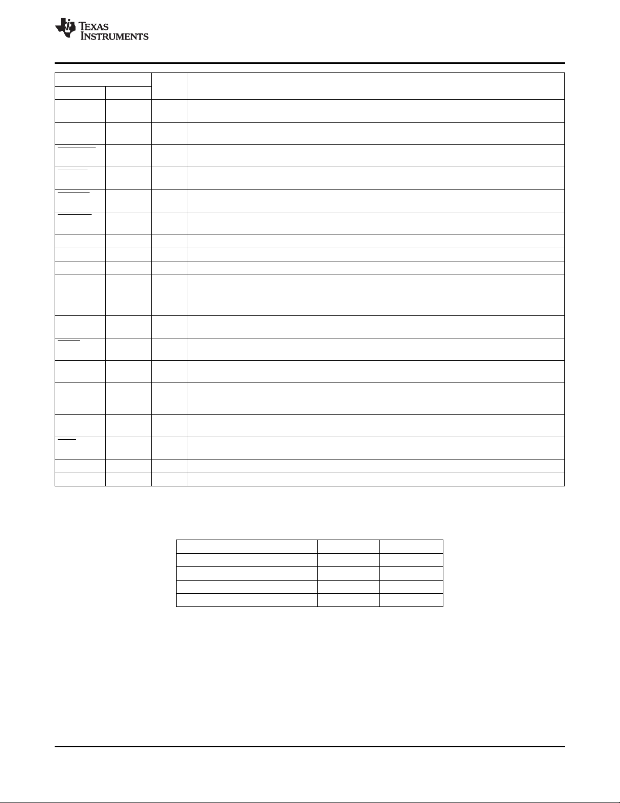
8052 Core
PWM
Counters
I
2
C
Control
Control/Status
Registers
Codec Port
Interface
2K x 8
SRAM
DMA0
DMA1
DMA2
DMA3
OEP
IEP
DMA Controller
and
USB Buffer Manager
4K ROM
8K RAM
USB Serial
OSC
PLL
ACG
Suspend
/Resume
Logic
PWM
I2C Bus
C-Port
Port3 Port1
USB
SOF
CLOCKS
6 MHz
Interface
Engine
TUSB3200A
www.ti.com
1.2 Functional Block Diagram
SLES018A–OCTOBER 2001–REVISED JULY 2010
Copyright © 2001–2010, Texas Instruments Incorporated Introduction 11
Submit Documentation Feedback
Product Folder Link(s): TUSB3200A
Page 12
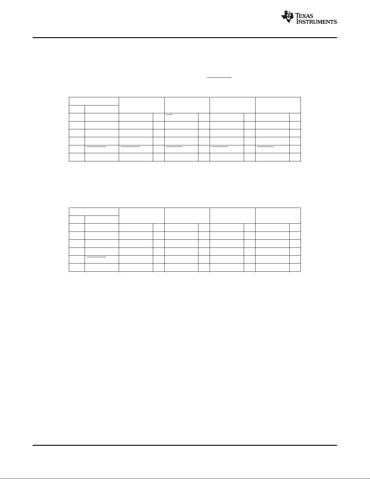
PAH Package
MCLKO2
MCLKO
DV
SCL
PLLFILI
XTALI
XTALO
AV
SS
MCLKI
DV
PLLOEN
P1.0
P1.1
P1.2
DV
SS
P3.3
P3.4
P3.5
DV
Dd
P3.0
P3.1
SDA
CSCHNE
38
37
36
35
34
33
32
31
30
29
28
27
1
2
3
4
5
6
7
8
9
10
11
12
13
(TOP VIEW)
MCLKI2
SS
DDS
CDATI
DV
DD
CDATO
CSYNC
CSCLK
DV
SS
P1.7
P1.6
P1.5
P1.4
P1.3
DV
DDS
PLLFILO
AV
DD
PWMO
PLLO
DV
SS
PUR
DP
DM
DV
DD
MRESET
TEST
EXTEN
RSTO
XINT
TUSB3200A
USB Streaming Controller (STC)
52-pin TQFP
CRESET
39
52 45 41 40
42
51 50
4849
47
44
43
46
14 21 25 26
24
15
16
1817 19
22 23
20
TUSB3200A
SLES018A–OCTOBER 2001–REVISED JULY 2010
1.3 Terminal Assignments − Normal Mode
www.ti.com
12 Introduction Copyright © 2001–2010, Texas Instruments Incorporated
Submit Documentation Feedback
Product Folder Link(s): TUSB3200A
Page 13
PAH Package
MCLKO2
MCLKO
DV
SCL
51 50
PLLFILI
XTALI
XTALO
AV
SS
MCLKI
DV
MCURD
MCUAD0
MCUAD1
MCUAD2
DV
SS
MCUA10
MCUALE
MCUINTO
DV
DD
MCUA8
MCUA9
SDA
CSCHNE
38
37
36
35
34
33
32
31
30
29
28
27
1
2
3
4
5
6
7
8
9
10
11
12
13
(TOP VIEW)
MCLKI2
SS
DDS
CDATI
DV
DD
CDATO
CSYNC
CSCLK
DV
SS
MCUAD7
MCUAD6
MCUAD5
MCUAD4
MCUAD3
DV
DDS
PLLFILO
AV
DD
PWMO
PLLO
DV
SS
PUR
DP
DM
DV
DD
MRESET
TEST
EXTEN
RSTO
XINT
MCUWR
USB Streaming Controller (STC)
52-pin TQFP
CRESET
TUSB3200A
52 45 41 40
42
51 50
4849
47
44
43
46
14 21 25 26
24
15
16
1817 19
22 23
20
TQFP
Texas Instruments
PackageType
Peripheral Device
Universal Serial Bus
52 pins PAH
T
3200A
USB PAH
Commercial Temperature Range
C
TUSB3200A
www.ti.com
1.4 Terminal Assignments − External MCU Mode
SLES018A–OCTOBER 2001–REVISED JULY 2010
1.5 Ordering Information
Copyright © 2001–2010, Texas Instruments Incorporated Introduction 13
Submit Documentation Feedback
Product Folder Link(s): TUSB3200A
Page 14
TUSB3200A
SLES018A–OCTOBER 2001–REVISED JULY 2010
www.ti.com
1.6 Terminal Functions − Normal Mode
TERMINAL
NAME NO.
AV
AV
DD
SS
2 3.3-V Analog supply voltage
49 Analog ground
CSCLK 34 I/O Codec port interface serial clock: CSCLK is the serial clock for the codec port interface used to clock
CSYNC 35 I/O Codec port interface frame sync: CSYNC is the frame synchronization signal for the codec port
CDATO 36 I/O Codec port interface serial data output: See Section 1.9 for details. This signal uses a 5-V compatible
CDATI 38 I/O Codec port interface serial data input: See Section 1.9 for details. This signal uses a 5-V compatible
CRESET 39 I/O Codec port interface reset output: See Section 1.9 for details. This signal uses a 5-V compatible
CSCHNE 40 I/O Codec port interface secondary channel enable: See Section 1.9 for details. This signal uses a 5-V
DP 7 I/O USB differential pair data signal plus: DP is the positive signal of the bidirectional USB differential pair
DM 8 I/O USB differential pair data signal minus: DM is the negative signal of the bidirectional USB differential
DV
DV
DV
DD
DDS
SS
9, 21, 3.3-V digital supply voltage
37
27, 43 5-V Digital supply voltage
5, 16, Digital ground
33, 46
EXTEN 12 I External MCU mode enable: Input used to enable the device for the external MCU mode. This signal
MCLKI 47 I Master clock input: An input that can be used as the master clock for the codec port interface or the
MCLKI2 48 I Master clock input 2: An input that can be used as the master clock for the codec port interface or the
MCLKO 44 O Master clock output: The output of the ACG that can be used as the master clock for the codec port
MCLKO2 45 O Master clock output 2: An output that can be used as the master clock for the codec port interface and
MRESET 10 I Master reset: An active low asynchronous reset for the device that resets all logic to the default state.
Not Used 22 I This pin is not used in the normal mode. This signal should be tied to digital ground for normal
P1.0 24 I/O General-purpose I/O port 1 bit 0: A bidirectional I/O port. This signal uses a 5-V compatible
P1.1 25 I/O General-purpose I/O port 1 bit 1: A bidirectional I/O port. This signal uses a 5-V compatible
P1.2 26 I/O General-purpose I/O port 1 bit 2: A bidirectional I/O port. This signal uses a 5-V compatible
P1.3 28 I/O General-purpose I/O port 1 bit 3: A bidirectional I/O port. This signal uses a 5-V compatible
P1.4 29 I/O General-purpose I/O port 1 bit 4: A bidirectional I/O port. This signal uses a 5-V compatible
P1.5 30 I/O General-purpose I/O port 1 bit 5: A bidirectional I/O port. This signal uses a 5-V compatible
P1.6 31 I/O General-purpose I/O port 1 bit 6: A bidirectional I/O port. This signal uses a 5-V compatible
P1.7 32 I/O General-purpose I/O port 1 bit 7: A bidirectional I/O port. This signal uses a 5-V compatible
I/O DESCRIPTION
the CSYNC, CDATO, CDATI, CRESET and CSCHNE signals. This signal uses a 5-V compatible
TTL/LVCMOS input/output buffer.
interface. This signal uses a 5-V compatible TTL/LVCMOS input/output buffer.
TTL/LVCMOS input/output buffer.
TTL/LVCMOS input/output buffer.
TTL/LVCMOS input/output buffer.
compatible TTL/LVCMOS input/output buffer.
used to connect the TUSB3200A device to the universal serial bus.
pair used to connect the TUSB3200A device to the universal serial bus.
uses a 3.3-V TTL/LVCMOS input buffer.
source for MCLKO2. This signal uses a 5-V to 3.3-V level shifting input buffer.
source for MCLKO2. This signal uses a 5-V to 3.3-V level shifting input buffer.
interface and the codec. This signal uses a 3.3-V TTL/LVCMOS output buffer.
the codec. This clock signal can also be used as a miscellaneous clock. This signal uses a 3.3-V
TTL/LVCMOS output buffer.
This signal uses a 3.3-V TTL/LVCMOS input buffer.
operation.
TTL/LVCMOS input/output buffer with an internal 100-µA active pullup.
TTL/LVCMOS input/output buffer with an internal 100-µA active pullup.
TTL/LVCMOS input/output buffer with an internal 100-µA active pullup.
TTL/LVCMOS input/output buffer with an internal 100-µA active pullup.
TTL/LVCMOS input/output buffer with an internal 100-µA active pullup.
TTL/LVCMOS input/output buffer with an internal 100-µA active pullup.
TTL/LVCMOS input/output buffer with an internal 100-µA active pullup.
TTL/LVCMOS input/output buffer with an internal 100-µA active pullup.
14 Introduction Copyright © 2001–2010, Texas Instruments Incorporated
Submit Documentation Feedback
Product Folder Link(s): TUSB3200A
Page 15
TUSB3200A
www.ti.com
TERMINAL
NAME NO.
P3.0 14 I/O General-purpose I/O port 3 bit 0: A bidirectional I/O port. This signal uses a 5-V compatible
P3.1 15 I/O General-purpose I/O port 3 bit 1: A bidirectional I/O port. This signal uses a 5-V compatible
P3.3 18 I/O General-purpose I/O port 3 bit 3: A bidirectional I/O port. This signal uses a 5-V compatible
P3.4 19 I/O General-purpose I/O port 3 bit 4: A bidirectional I/O port. This signal uses a 5-V compatible
P3.5 20 I/O General-purpose I/O port 3 bit 5: A bidirectional I/O port. This signal uses a 5-V compatible
PLLFILI 52 I PLL loop filter input: Input to on-chip PLL from external filter components.
PLLFILO 1 O PLL loop filter output: Output from on-chip PLL to external filter components.
PLLO 4 O PLL output: The 48-MHz output of the PLL used for diagnostic purposes only. This signal uses a 3.3-V
PLLOEN 23 I PLL output enable: An input used to enable the PLLO output signal. This signal uses a 5-V compatible
PWMO 3 O PWM output: Output of the pulse width modulation circuit. PWMO This signal uses a 3.3-V to 5-V
PUR 6 O USB data signal plus pullup resistor connect: PUR is used to connect the pullup resistor on the DP
RSTO 13 O Reset output: Output that is active while the master reset input or the USB reset is active. This signal
SCL 42 O I2C interface serial clock: SCL is the clock signal for the I2C serial interface. This signal uses a 3.3-V to
SDA 41 I/O I2C interface serial data input/output: SDA is the bidirectional data signal for the I2C serial interface.
TEST 11 I Test mode enable: Input used to enable the device for the factory test mode. This signal uses a 3.3-V
XINT 17 I External interrupt: An active low input used by external circuitry to interrupt the on-chip 8052 MCU.
XTALI 51 I Crystal input: Input to the on-chip oscillator from an external 6-MHz crystal.
XTALO 50 O Crystal Output: Output from the on-chip oscillator to an external 6-MHz crystal.
I/O DESCRIPTION
TTL/LVCMOS input/output buffer with an internal 100-µA active pullup. Can also be used as UART
RxD.
TTL/LVCMOS input/output buffer with an internal 100-µA active pullup. Can also be used as UART
TxD.
TTL/LVCMOS input/output buffer with an internal 100-µA active pullup.
TTL/LVCMOS input/output buffer with an internal 100-µA active pullup.
TTL/LVCMOS input/output buffer with an internal 100-µA active pullup.
TTL/LVCMOS output buffer.
input buffer.
CMOS level shifting output buffer.
signal to 3.3-V or a 3-state. When the DP signal is connected to 3.3-V the host PC should detect the
connection of the TUSB3200A device to the universal serial bus. This signal uses a 3.3-V
TTL/LVCMOS output buffer.
uses a 3.3-V TTL/LVCMOS output buffer.
5-V TTL level shifting open drain output buffer.
This signal uses a 3.3-V to 5-VTTL level shifting open drain output buffer and a 5-V to 3.3-V TTL level
shifting input buffer.
TTL/LVCMOS input buffer.
This signal uses a 5-V compatible input buffer.
SLES018A–OCTOBER 2001–REVISED JULY 2010
Copyright © 2001–2010, Texas Instruments Incorporated Introduction 15
Submit Documentation Feedback
Product Folder Link(s): TUSB3200A
Page 16
TUSB3200A
SLES018A–OCTOBER 2001–REVISED JULY 2010
www.ti.com
1.7 Terminal Functions − External MCU Mode
TERMINAL
NAME NO.
AV
AV
DD
SS
2 3.3-V Analog supply voltage
49 Analog ground
CSCLK 34 I/O Codec port interface serial clock: CSCLK is the serial clock for the codec port interface used to clock
CSYNC 35 I/O Codec port interface frame sync: CSYNC is the frame synchronization signal for the codec port
CDATO 36 I/O Codec port interface serial data output: See Section 1.9 for details. This signal uses a 5-V compatible
CDATI 38 I/O Codec port interface serial data input: See Section 1.9 for details. This signal uses a 5-V compatible
CRESET 39 I/O Codec port interface reset output: See Section 1.9 for details. This signal uses a 5-V compatible
CSCHNE 40 I/O Codec port interface secondary channel enable: See Section 1.9 for details. This signal uses a 5-V
DP 7 I/O USB differential pair data signal plus: DP is the positive signal of the bidirectional USB differential pair
DM 8 I/O USB differential pair data signal minus: DM is the negative signal of the bidirectional USB differential
DV
DV
DV
DD
DDS
SS
9, 21, 37 3.3-V digital supply voltage
27, 43 5-V Digital supply voltage
5, 16, 33, Digital ground
46
EXTEN 12 I External MCU mode enable: Input used to enable the device for the external MCU mode. This signal
MCLKI 47 I Master clock input: An input that can be used as the master clock for the codec port interface or the
MCLKI2 48 I Master clock input 2: An input that can be used as the master clock for the codec port interface or the
MCLKO 44 O Master clock output: The output of the ACG that can be used as the master clock for the codec port
MCLKO2 45 O Master clock output 2: An output that can be used as the master clock for the codec port interface and
MCUAD0 24 I/O MCU Multiplexed address/data bit 0: Multiplexed address bit 0/data bit 0 for external MCU access to
MCUAD1 25 I/O MCU multiplexed address/data bit 1: Multiplexed address bit 1/data bit 1 for external MCU access to
MCUAD2 26 I/O MCU multiplexed address/data bit 2: Multiplexed address bit 2/data bit 2 for external MCU access to
MCUAD3 28 I/O MCU multiplexed address/data bit 3: Multiplexed address bit 3/data bit 3 for external MCU access to
MCUAD4 29 I/O MCU multiplexed address/data bit 4: Multiplexed address bit 4/data bit 4 for external MCU access to
MCUAD5 30 I/O MCU multiplexed address/data bit 5: Multiplexed address bit 5/data bit 5 for external MCU access to
MCUAD6 31 I/O MCU multiplexed address/data bit 6: Multiplexed address bit 6/data bit 6 for external MCU access to
MCUAD7 32 I/O MCU multiplexed address/data bit 7: Multiplexed address bit 7/data bit 7 for external MCU access to
MCUA8 14 I MCU address bit 8: Multiplexed address bit 8 for external MCU access to the TUSB3200A external
MCUA9 15 I MCU address bit 9: Multiplexed address bit 9 for external MCU access to the TUSB3200A external
I/O DESCRIPTION
the CSYNC, CDATO, CDATI, CRESET and CSCHNE signals. This signal uses a 5-V compatible
TTL/LVCMOS input/output buffer.
interface. This signal uses a 5-V compatible TTL/LVCMOS input/output buffer.
TTL/LVCMOS input/output buffer.
TTL/LVCMOS input/output buffer.
TTL/LVCMOS input/output buffer.
compatible TTL/LVCMOS input/output buffer.
used to connect the TUSB3200A device to the universal serial bus.
pair used to connect the TUSB3200A device to the universal serial bus.
uses a 3.3-V TTL/LVCMOS input buffer.
source for MCLKO2. This signal uses a 5-V to 3.3-V level shifting input buffer.
source for MCLKO2. This signal uses a 5-V to 3.3-V level shifting input buffer.
interface and the codec. This signal uses a 3.3-V TTL/LVCMOS output buffer.
the codec. This clock signal can also be used as a miscellaneous clock. This signal uses a 3.3-V
TTL/LVCMOS output buffer.
the TUSB3200A external data memory space.
the TUSB3200A external data memory space.
the TUSB3200A external data memory space.
the TUSB3200A external data memory space.
the TUSB3200A external data memory space.
the TUSB3200A external data memory space.
the TUSB3200A I/O external data memory space.
the TUSB3200A external data memory space.
data memory space.
data memory space.
16 Introduction Copyright © 2001–2010, Texas Instruments Incorporated
Submit Documentation Feedback
Product Folder Link(s): TUSB3200A
Page 17
TUSB3200A
www.ti.com
TERMINAL
NAME NO.
MCUA10 18 I MCU address bit 10: Multiplexed address bit 10 for external MCU access to the TUSB3200A external
MCUALE 19 I MCU address latch enable: Address latch enable for external MCU access to the TUSB3200A external
MCUINTO 20 O MCU interrupt output: Interrupt output to be used for external MCU INTO input signal. All internal
MCURD 23 I MCU read strobe: Read strobe for external MCU read access to the TUSB3200A external data
MCUWR 22 I MCU write strobe: Write strobe for external MCU write access to the TUSB3200A external data
MRESET 10 I Master reset: An active low asynchronous reset for the device that resets all logic to the default state.
Not Used 4 O This pin is not used in the external MCU mode.
PLLFILI 52 I PLL loop filter input: Input to on-chip PLL from external filter components.
PLLFILO 1 O PLL loop filter output: Output to on-chip PLL from external filter components.
PUR 6 O USB data signal plus pullup resistor connect: PUR is used to connect the pullup resistor on the DP
PWMO 3 O PWM output: Output of the pulse width modulation circuit. This signal uses a 3.3-V to 5-V CMOS level
RSTO 13 O Reset output: Output that is active while the master reset input or the USB reset is active. This signal
SCL 42 O I2C interface serial clock: SCL is the clock signal for the I2C serial interface. This signal uses a 3.3-V
SDA 41 I/O I2C interface serial data input/output: SDA is the bidirectional data signal for the I2C serial interface.
TEST 11 I Test mode enable: Input used to enable the device for the factory test mode. This signal uses a 3.3-V
XINT 17 I External interrupt: An active low input used by external circuitry to interrupt the on-chip 8052 MCU.
XTALI 51 I Crystal input: Input to the on-chip oscillator from an external 6-MHz crystal.
XTALO 50 O Crystal output: Output from the on-chip oscillator to an external 6-MHz crystal.
I/O DESCRIPTION
data memory space.
data memory space.
TUSB3200A interrupt sources are ORed together to generate this output signal.
memory space.
memory space.
This signal uses a 3.3-V TTL/LVCMOS input buffer.
signal to 3.3-V or a 3-state. When the DP signal is connected to 3.3-V the host PC should detect the
connection of the TUSB3200A device to the universal serial bus. This signal uses a 3.3-V
TTL/LVCMOS output buffer.
shifting output buffer.
uses a 3.3-V TTL/LVCMOS output buffer.
to 5-V TTL level shifting open drain output buffer.
This signal uses a 3.3-V to 5-V TTL level shifting open drain output buffer and a 5-V to 3.3-V TTL level
shifting input buffer.
TTL/LVCMOS input buffer.
This signal uses a 5-V compatible input buffer.
SLES018A–OCTOBER 2001–REVISED JULY 2010
1.8 Device Operation Modes
The EXTEN and TEST pins define the mode that the TUSB3200A will be in after reset.
MODE EXTEN TEST
Normal mode – internal MCU 0 0
External MCU mode 1 0
Factory test 0 1
Factory test 1 1
Copyright © 2001–2010, Texas Instruments Incorporated Introduction 17
Submit Documentation Feedback
Product Folder Link(s): TUSB3200A
Page 18
TUSB3200A
SLES018A–OCTOBER 2001–REVISED JULY 2010
1.9 Terminal Assignments for Codec Port Interface Modes
The codec port interface has eight modes of operation that support AC97, I2S, and AIC codecs. There is
also a general-purpose mode that is not specific to a serial interface. The mode is programmed by writing
to the mode select field of the codec port interface configuration register 1 (CPTCNF1). The codec port
interface terminals CSYNC, CSCLK, CDATO, CDATI, CRESET, and CSCHNE take on functionality
appropriate to the mode programmed as shown in the following tables.
TERMINAL
NO. NAME
35 CSYNC CSYNC
34 CSCLK CSCLK
36 CDATO CDATO O DOUT O SD_OUT O SD_OUT O
38 CDATI CDATI I DIN I SD_IN I SD_IN1 I
39 CRESET CRESET O RESET O RESET O RESET O
40 CSCHNE NC
(1) Signal names and I/O direction are with respect to the TUSB3200A device. The signal names used for
the TUSB3200A terminals for the various codec port interface modes reflect the nomenclature used by
the codec devices.
(2) The CSYNC and CSCLK signals can be programmed as either an input or an output in the
general-purpose mode.
(3) NC indicates no connection for the terminal in a particular mode. The TUSB3200A device drives the
signal as an output for these cases.
(1)
GP AIC AC '97 v1.X AC '97 v2.X
MODE 0 MODE 1 MODE 2 MODE 3
(2)
I/O FS O SYNC O SYNC O
(2)
(3)
I/O SCLK O BIT_CLK I BIT_CLK I
O FC O NC
www.ti.com
(3)
O SD_IN2 I
TERMINAL
NO. NAME
35 CSYNC LRCK O LRCK O LRCK O LRCK O
34 CSCLK SCLK O SCLK O SCLK O SCLK O
36 CDATO SDOUT1 O SDOUT1 O SDOUT1 O SDOUT1 O
38 CDATI SDOUT2 O SDOUT2 O SDIN1 I SDOUT2 O
39 CRESET SDOUT3 O SDIN1 I SDIN2 I SDOUT3 O
40 CSCHNE SDIN1 I SDIN2 I SDIN3 I SDOUT4 O
I2S I2S I2S I2S
MODE 4 MODE 5 MODE 6 MODE 7
18 Introduction Copyright © 2001–2010, Texas Instruments Incorporated
Submit Documentation Feedback
Product Folder Link(s): TUSB3200A
Page 19

TUSB3200A
www.ti.com
2 Description
2.1 Architectural Overview
2.1.1 Oscillator and PLL
Using an external 6-MHz crystal, the TUSB3200A derives the fundamental 48-MHz internal clock signal
using an on-chip oscillator and PLL. Using the PLL output, the other required clock signals are generated
by the clock generator and adaptive clock generator.
2.1.2 Clock Generator and Sequencer Logic
Utilizing the 48-MHz input from the PLL, the clock generator logic generates all internal clock signals,
except for the codec port interface master clock (MCLK) and serial clock (CSCLK) signals. The
TUSB3200A internal clocks include the 48-MHz clock, a 24-MHz clock, a 12-MHz clock and a USB clock.
The USB clock also has a frequency of 12-MHz. The USB clock is the same as the 12-MHz clock when
the TUSB3200A is transmitting data and is derived from the data when the TUSB3200A is receiving data.
To derive the USB clock when receiving USB data, the TUSB3200A utilizes an internal digital PLL (DPLL)
that uses the 48-MHz clock.
The sequencer logic controls the access to the SRAM used for the USB endpoint configuration blocks and
the USB endpoint buffer space. The SRAM can be accessed by the MCU, USB buffer manager (UBM) or
DMA channels. The sequencer controls the access to the memory using a round robin fixed priority
arbitration scheme. This basically means that the sequencer logic generates grant signals for the MCU,
UBM and DMA channels at a predetermined fixed frequency.
SLES018A–OCTOBER 2001–REVISED JULY 2010
2.1.3 Adaptive Clock Generator (ACG)
The adaptive clock generator is used to generate a master clock output signal (MCLKO) to be used by the
codec port interface and the codec device. To synchronize the sample rate conversion of data by the
codec to the USB frame rate, the MCLKO signal generated by the adaptive clock generator must be used.
The synchronization of the MCLKO signal to the USB frame rate is controlled by the MCU by
programming the adaptive clock generator frequency value. The MCLKO frequency is monitored by the
MCU and updated as required. For asynchronous operation, an external source can be used to generate
a master clock input signal (MCLKI) to be used by the codec port interface. In this scenario, the codec
device should also use the same master clock signal (MCLKI).
2.1.4 USB Transceiver
The TUSB3200A provides an integrated transceiver for the USB port. The transceiver includes a
differential output driver, a differential input receiver and two single ended input buffers. The transceiver
connects to the USB DP and DM signal terminals.
2.1.5 USB Serial Interface Engine (SIE)
The serial interface engine logic manages the USB packet protocol requirements for the packets being
received and transmitted on the USB by the TUSB3200A device. For packets being received, the SIE
decodes the packet identifier field (PID) to determine the type of packet being received and to ensure the
PID is valid. For token packets and data packets being received, the SIE calculates the packet cycle
redundancy check (CRC) and compares the value to the CRC contained in the packet to verify that the
packet was not corrupted during transmission. For token packets and data packets being transmitted, the
SIE generates the CRC that is transmitted with the packet. For packets being transmitted, the SIE also
generates the synchronization field (SYNC) that is an eight bit filed at the beginning of each packet. In
addition, the SIE generates the correct PID for all packets being transmitted. Another major function of the
SIE is the overall serial-to-parallel conversion of the data packets being received and the parallel-to-serial
conversion of the data packets being transmitted.
Copyright © 2001–2010, Texas Instruments Incorporated Description 19
Submit Documentation Feedback
Product Folder Link(s): TUSB3200A
Page 20

TUSB3200A
SLES018A–OCTOBER 2001–REVISED JULY 2010
2.1.6 USB Buffer Manager (UBM)
The USB buffer manager provides the control logic that interfaces the SIE to the USB endpoint buffers.
One of the major functions of the UBM is to decode the USB function address to determine if the host PC
is addressing the TUSB3200A device USB peripheral function. In addition, the endpoint address field and
direction signal are decoded to determine which particular USB endpoint is being addressed. Based on
the direction of the USB transaction and the endpoint number, the UBM will either write or read the data
packet to/from the appropriate USB endpoint data buffer.
2.1.7 USB Frame Timer
The USB frame timer logic receives the start of frame (SOF) packet from the host PC each USB frame.
Each frame, the logic stores the 11-bit frame number value from the SOF packet in a register and asserts
the internal SOF signal. The frame number register can be read by the MCU and the value can be used
as a time stamp. For USB frames in which the SOF packet is corrupted or not received, the frame timer
logic will generate a pseudo start of frame (PSOF) signal and increment the frame number register.
2.1.8 USB Suspend and Resume Logic
The USB suspend and resume logic detects suspend and resume conditions on the USB. This logic also
provides the internal signals used to control the TUSB3200A device when these conditions occur. The
capability to resume operation from a suspend condition with a locally generated remote wake-up event is
also provided.
www.ti.com
2.1.9 MCU Core
The TUSB3200A uses an 8-bit microcontroller core that is based on the industry standard 8052. The MCU
is software compatible with the 8052, 8032, 80C52, 80C53, and 87C52 MCUs. The 8052 MCU is the
processing core of the TUSB3200A and handles all USB control, interrupt and bulk endpoint transfers. In
addition, the MCU can also be the source or sink for USB isochronous endpoint transfers.
2.1.10 MCU Memory
In accordance with the industry standard 8052, the TUSB3200A MCU memory is organized into program
memory, external data memory and internal data memory. A 4K byte boot ROM is used to download the
application code to an 8K byte RAM that is mapped to the program memory space. The external data
memory includes the USB endpoint configuration blocks, USB data buffers, and memory mapped
registers. The total external data memory space used is 2K bytes. A total of 256 bytes are provided for the
internal data memory.
2.1.11 USB Endpoint Configuration Blocks and Endpoint Buffer Space
The USB endpoint configuration blocks are used by the MCU to configure and operate the required USB
endpoints for a particular application. In addition to the control endpoint, the TUSB3200A supports a total
of seven in endpoints and seven out endpoints. A set of six bytes is provided for each endpoint to specify
the endpoint type, buffer address, buffer size, and data packet byte count.
The USB endpoint buffer space provided is a total of 1832 bytes. The space is totally configurable by the
MCU for a particular application. Therefore, the MCU can configure each buffer based on the total number
of endpoints to be used, the maximum packet size to be used for each endpoint, and the selection of
single or double buffering.
2.1.12 DMA Controller
Four DMA channels are provided to support the streaming of data for USB isochronous endpoints. Each
DMA channel can support one USB isochronous endpoint, either in or out. The DMA channels are used to
stream data between the USB endpoint data buffers and the codec port interface. The USB endpoint
number and direction can be programmed for each DMA channel. Also, the codec port interface time slots
to be serviced by each DMA channel can be programmed.
20 Description Copyright © 2001–2010, Texas Instruments Incorporated
Submit Documentation Feedback
Product Folder Link(s): TUSB3200A
Page 21
TUSB3200A
www.ti.com
2.1.13 Codec Port Interface
The TUSB3200A provides a configurable full-duplex bidirectional serial interface that can connect to a
codec or another device for streaming USB Isochronous data. The interface can be configured to support
several different industry standard protocols, including AC '97 1.X, AC '97 2.X, and I2S.
2.1.14 I2C Interface
The I2C interface logic provides a two-wire serial interface that can be used by the 8052 MCU to access
other ICs. The TUSB3200A is an I2C master device only and supports single byte or multiple byte read
and write operations. The interface can be programmed to operate at either 100 kbps or 400 kbps. The
protocol supports 8-bit or 16-bit addressing for accessing the I2C slave device memory locations.
2.1.15 Pulse Width Modulation (PWM) Output
The TUSB3200A provides a pulse width modulation output with programmable frequency and pulse width.
The frequency can be programmed from 732 Hz to 93.7 kHz with an 8-bit register. The pulse width of the
output signal is set with a 16-bit register.
2.1.16 General-Purpose IO Ports (GPIO)
The TUSB3200A provides two general-purpose IO ports that are controlled by the internal 8052 MCU. The
two ports, port 1 and port 3, are 8-bits and 5-bits, respectively. Note that port 3 bit locations 2, 6, and 7
have been used in the TUSB3200A for other functionality. Therefore these three bit locations are not
available for GPIO use. Port 3 bit location 2 has been used as the external interrupt (XINT) input to the
TUSB3200A. Port 3 bit locations 6 and 7 have been used as the external MCU write strobe and read
strobe inputs for the external MCU mode of operation.
SLES018A–OCTOBER 2001–REVISED JULY 2010
Each bit of both ports can be independently used as either an input or output. Hence each port bit consists
of an output buffer, an input buffer, and a pullup resistor (the pullups are not, strictly speaking, resistors;
they are 100-µA pullup active terminators). The pullup resistors on the GPIO pins can be disabled using
the PUDIS bit in the global control register.
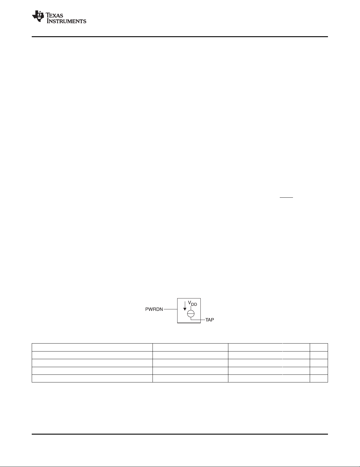
2.1.16.1 External Pullup Macro
This is the equivalent circuit of the pullup "resistor", from the silicon library used to implement the
TUSB3200A.
Logic Symbol (Positive Logic)
Table 2-1. Electrical Characteristics of Pullup Resistors
PARAMETER TEST CONDITIONS MIN TYP MAX UNIT
I
FI Input loading factor TAP 1.65 pF
FI Input loading factor PWRDN 2.50 SL
C
(1) When PWRDN = H, the current source is turned off.
Output current VO= 0 V –35.98 –90.67 –197.38 µA
O
Equivalent power dissipation capacitance 0.04 pF
pd
(1)
NOTE: For use with 3-V I/Os only.
Copyright © 2001–2010, Texas Instruments Incorporated Description 21
Submit Documentation Feedback
Product Folder Link(s): TUSB3200A
Page 22

TUSB3200A
SLES018A–OCTOBER 2001–REVISED JULY 2010
2.1.17 Interrupt Logic
The interrupt logic monitors the various conditions that can cause an interrupt and asserts the interrupt 0
(INT0) input to the 8052 MCU accordingly. All of the TUSB3200A internal interrupt sources and the
external interrupt (XINT) input are ORed together to generate the INT0 signal. An interrupt vector register
is provided that is used by the MCU to identify the interrupt source.
2.1.18 Reset Logic
An external master reset (MRESET) input signal that is asynchronous to the internal clocks is used to
reset the TUSB3200A logic. In addition to the master reset, the TUSB3200A logic can be reset with the
USB reset from the host PC. The TUSB3200A also provides a reset output (RSTO) signal that can be
used by external devices. This signal is asserted when either a master reset or USB reset occurs.
2.2 Device Operation
The operation of the TUSB3200A is explained in the following sections. For additional information on USB,
see the universal serial bus Specification version 1.1.
2.2.1 Clock Generation
The TUSB3200A requires an external 6-MHz crystal and PLL loop filter components connected as shown
in Figure 4-1 to derive all the clocks needed for both USB and codec operation. Using the low frequency
6-MHz crystal and generating the required higher frequency clocks internal to the IC is a major advantage
regarding EMI.
www.ti.com
2.2.2 Device Initialization
After a power-on reset is applied to the TUSB3200A device, the 8052 MCU will execute a boot loader
program from the 4k or 8k byte boot ROM mapped to the program memory space. During device
initialization, the boot loader program downloads the application program code from an external EEPROM
through the I2C interface. This requires that a binary image of the application code be written to the 8K
byte code RAM in the TUSB3200A device.
All memory mapped registers are initialized to a default value as defined in Section A, MCU Memory and
Memory- Mapped Registers. The TUSB3200A device powers up with a default function address of zero
and disconnected from the USB.
2.2.2.1 Boot Load from EEPROM
Loading the application code from an external serial EEPROM requires a preprogrammed memory device
containing an informative header and the application code. While the application code is being
downloaded, the TUSB3200A will remain disconnected from the USB. When the code download is
complete, execution of the application code should connect the TUSB3200A to the USB. In this situation,
the TUSB3200A will enumerate using the vendor ID and product ID contained in the application code.
22 Description Copyright © 2001–2010, Texas Instruments Incorporated
Submit Documentation Feedback
Product Folder Link(s): TUSB3200A
Page 23
TUSB3200A
www.ti.com
2.2.2.2 EEPROM Header
An EEPROM header precedes the application code in the EEPROM device. The bootloader uses the
information in the header as it loads the application code into RAM. Table 2-2 shows the format and
information contained in the header.
OFFSET TYPE SIZE VALUE
0 Signature 4 0x04513200
4 Header size 1 Header size
5 Version 1 Firmware version
6 1
EEPROM type
7 1
Data type
8 Data size 2 Data payload only size
10 2 Check sum of the data payload beginning at location Check Sum
Check sum
12 Data Data payload
SLES018A–OCTOBER 2001–REVISED JULY 2010
Table 2-2. EEPROM Header
0x01 = Reserved
0x02 = Reserved
0x03 = Reserved
0x04 = Reserved
0x05 = Reserved
0x06 = Reserved
0x07 = Reserved
0x08 = Reserved
0x09 = 24C32
0x0A =24C64
0x0B…0xFF = Reserved
0x01 = Application code
0x02…0xFF = Reserved
+ 2
The signature field is used for the detection of a EEPROM device connected to the TUSB3200A. The
header size field supports future updates of the header. Data begins right after the header. The version
field identifies the header version. The EEPROM type field identifies the specific EEPROM device being
used. The data type field describes the nature of data stored in the EEPROM (application code). The data
size field holds the length of the data payload starting from the end of the header. The check sum field
contains the check sum for the data payload portion of the EEPROM.
2.2.2.3 Application Code
Application firmware is stored as a binary image of the code. The binary image is mapped to the MCU
program memory space starting at address zero and is stored in the EEPROM as a continuous linear
block starting after the header information. A utility program is available that converts a file in Intel
hexidecimal format to a binary image data file and appends it to the header.
2.2.2.4 EEPROM Device Type
The TUSB3200A boot loader program supports several different types of serial EEPROM devices. The
boot loader program will automatically identify the EEPROM type from the header information and use the
correct serial interface protocol accordingly. The boot loader program uses an I2C slave device address of
A0h for the serial EEPROM device.
Copyright © 2001–2010, Texas Instruments Incorporated Description 23
Submit Documentation Feedback
Product Folder Link(s): TUSB3200A
Page 24

TUSB3200A
SLES018A–OCTOBER 2001–REVISED JULY 2010
These EEPPROM devices require an I2C device address in addition to a two byte data word address.
These devices require the full 7-bit I2C device address. Depending on the memory size of the EEPROM
device being used, the most significant three or four bits of the two byte data word address are don't care
bits. The EEPROM types supported are: 24C32 and 24C64
All of these EEPROM devices can be used for storing and loading application code. However most
applications will use devices which are capable of storing up to 8K bytes of program code.
2.2.3 USB Enumeration
USB enumeration is accomplished by interaction between the host PC software and the TUSB3200A
code. After power-on reset the boot loader code first reads the information from the EEPROM, then runs
the application code. The application code connects the TUSB3200A to the USB. During the enumeration,
the application code identifies the device as an application specific device and the host loads the
appropriate host driver(s). The boot loader and application code both use the CONT, SDW, and FRSTE
bits to control the enumeration process. The function connect (CONT) bit is set to a 1 by the MCU to
connect the TUSB3200A device to the USB. When this bit is set to a 1, the USB data plus pullup resistor
(PUR) output signal is enabled, which will connect the pullup on the PCB to the TUSB3200A 3.3-V digital
supply voltage. When this bit is cleared to a 0, the PUR output is in the 3-state mode. This bit is not
affected by a USB reset. The shadow the boot ROM (SDW) bit is set to a 1 by the MCU to switch the
MCU memory configuration from boot loader mode to normal operating mode. The function reset enable
(FRSTE) bit is set to a 1 by the MCU to enable the USB reset to reset all internal logic including the MCU.
However, the shadow the ROM (SDW) and the USB function connect (CONT) bits will not be reset. When
this bit is set, the reset output (RSTO) signal from the TUSB3200A device will also be active when a USB
reset occurs. This bit is not affected by USB reset.
www.ti.com
2.2.4 USB Reset
The TUSB3200A can detect a USB reset condition. When the reset occurs, the TUSB3200A responds by
setting the function reset (RSTR) bit in the USB status register (USBSTA). If the corresponding function
reset bit in the USB interrupt mask register is set, an MCU interrupt will be generated and the USB
function reset (0x17) vector will appear in the interrupt vector register (VECINT).
The function reset enable bit (FRSTE) in the USB control register (USBCTL) is used to control the extent
to which the internal logic is reset. The function reset enable bit is set to a 1 by the MCU to enable the
USB reset to reset all internal logic including the MCU. However, the shadow the ROM (SDW) and the
USB function connect (CONT) bits will not be reset. When this bit is set, the reset output (RSTO) signal
from the device will also be active when a USB reset occurs. This bit is not affected by USB reset.
2.2.5 USB Suspend and Resume Modes
All USB devices must support the suspend and resume modes. During the suspend mode, USB devices
that are bus powered must enter a low power suspend state. If the USB peripheral device is not bus
powered, then entering the low power suspend state is not required. A suspend condition is defined as a
constant idle state on the bus for more than 3.0ms. A USB device must actually be in the suspend state
no more than 10 ms after the suspend condition is detected. There are two ways for the TUSB3200A
device to exit the suspend mode, which are 1) detection of USB resume signaling and 2) detection of a
local remote wake-up event.
2.2.5.1 USB Suspend Mode
When a suspend condition is detected on the USB, the suspend/resume logic will set the function suspend
request bit (SUSR) in the USB status register. As a result, the function suspend request interrupt (SUSR)
will be generated. To enter the low power suspend state and disable all TUSB3200A device clocks, the
MCU firmware should set the idle mode bit (IDL), which is bit 0 in the MCU power control (PCON) register.
The instruction that sets the IDL bit will be the last instruction executed before the MCU goes to idle mode.
In idle mode, the MCU status is preserved. Note that the low power suspend state is a state in which the
TUSB3200A clocks are disabled and the IC will consume the least amount of power possible.
24 Description Copyright © 2001–2010, Texas Instruments Incorporated
Submit Documentation Feedback
Product Folder Link(s): TUSB3200A
Page 25

TUSB3200A
www.ti.com
2.2.5.2 USB Resume Mode
When the TUSB3200A is in a suspend state, any non-idle signaling on the USB will be detected by the
suspend/resume logic and device operation will be resumed. As a result of the resume signaling being
detected, the TUSB3200A clocks will be enabled, the function resume request bit (RESR) will be set, and
the function resume request interrupt (RESR) will be generated. The function resume request interrupt to
the MCU will automatically clear the idle mode bit in the PCON register. As a result, MCU operation will
resume with servicing the new interrupt. After the RETI from the ISR, the next instruction to be executed
will be the one following the instruction that set the IDL bit. Note that if the low power suspend state was
not entered by setting the IDL bit, the clocks will already be enabled and the IDL bit will already be
cleared.
2.2.5.3 USB Remote Wake-Up Mode
The TUSB3200A device has the capability to remotely wake-up the USB by generating resume signaling
upstream. Note that this feature must be enabled by the host software with the SET_FEATURE
DEVICE_REMOTE_WAKEUP request. The remote wake-up resume signaling should not be generated
until the suspend state has been active for at least 5 ms. In addition, the remote wake-up resume
signaling must be generated for at least 1ms but for no more than 15 ms. When the TUSB3200A is in the
low power suspend state, asserting the external interrupt input (XINT) to the device will enable the clocks
and generate the XINT interrupt. The XINT interrupt to the MCU will automatically clear the idle mode bit
in the PCON register. As a result, MCU operation will resume with servicing the new interrupt. After the
RETI from the ISR, the next instruction to be executed will be the one following the instruction that set the
IDL bit. Please note that if the low power suspend state was not entered by setting the IDL bit, the clocks
will already be enabled and the IDL bit will already be cleared. When the firmware sets the remote
wake-up request bit (RWUP) in the USB control register, the suspend/resume logic will generate the
resume signaling upstream on the USB.
SLES018A–OCTOBER 2001–REVISED JULY 2010
2.2.6 Power Supply Sequencing
Turning power supplies on and off with a mixed 5-V/3.3-V system is an important consideration. To avoid
possible damage to the TUSB3200A device, proper power sequencing is required. The turnon
requirement is that the 5-V and 3.3-V power supplies should start ramping from 0 volts and reach 95
percent of the final voltage values within 25 ms of each other. The turnoff requirement is that the 5-V and
3.3-V power supplies should start ramping from the steady-state voltage and reach 5 percent of these
values within 25 ms of each other. In addition, the difference between the two voltages should never
exceed 3.6-V while turning on or off. Normally, in a mixed voltage system, the 3.3-V supply is generated
from a voltage regulator running from the 5-V supply. A voltage regulator, such as the Texas Instrument's
TP7133, can be used to meet these power sequencing requirements.
2.2.7 USB Transfers
The TUSB3200A device supports all the USB data transfer types, which are control, bulk, interrupt, and
isochronous. In accordance with the USB specification, endpoint zero is reserved for the control endpoint
and is bidirectional. In addition to the control endpoint, the TUSB3200A is capable of supporting up to 7 in
endpoints and 7 out endpoints. These additional endpoints can be configured as bulk, interrupt, or
isochronous endpoints. The MCU handles all control, bulk, and interrupt endpoint transactions. In addition
the MCU can handle isochronous endpoint transactions, such as a rate feedback endpoint to the host PC.
However, for streaming isochronous data between the host PC and the codec interface port, the DMA
channels are provided.
2.2.7.1 Controls Transfers
Control transfers are used for configuration, command, and status communication between the host PC
and the TUSB3200A device. Control transfers to the TUSB3200A device use in endpoint 0 and out
endpoint 0. The three types of control transfers are control write, control write with no data stage, and
control read. Note that the control endpoint must be initialized before connecting the TUSB3200A device
to the USB.
Copyright © 2001–2010, Texas Instruments Incorporated Description 25
Submit Documentation Feedback
Product Folder Link(s): TUSB3200A
Page 26

TUSB3200A
SLES018A–OCTOBER 2001–REVISED JULY 2010
2.2.7.1.1 Control Write Transfer (Out Transfer)
The host PC uses a control write transfer to write data to the USB function. A control write transfer
consists of a setup stage transaction, at least one out data stage transaction, and an in status stage
transaction.
The steps to be followed for a control write transfer are as follows:
1. MCU initializes in endpoint 0 and out endpoint 0 by programming the appropriate USB endpoint
configuration blocks. This entails programming the buffer size and buffer base address, selecting the
buffer mode, enabling the endpoint interrupt, initializing the TOGGLE bit, enabling the endpoint, and
clearing the NACK bit for both in endpoint 0 and out endpoint 0.
Setup Stage Transaction:
2. The host PC sends a setup token packet followed by the setup data packet addressed to out endpoint
0. If the data is received without an error, then the UBM will write the data to the setup data packet
buffer, set the setup stage transaction (SETUP) bit to a 1 in the USB status register, return an ACK
handshake to the host PC, and assert the setup stage transaction interrupt. Note that as long as the
setup transaction (SETUP) bit is set to a 1, the UBM will return a NAK handshake for any data stage or
status stage transactions regardless of the endpoint 0 NACK or STALL bit values.
3. The MCU services the interrupt and reads the setup data packet from the buffer then decodes the
command. If the command is not supported or valid, the MCU should set the STALL bit in the out
endpoint 0 configuration byte and the in endpoint 0 configuration byte before clearing the setup stage
transaction (SETUP) bit. This will cause the device to return a STALL handshake for any data stage or
status stage transactions. After reading the data packet and decoding the command, the MCU should
clear the interrupt, which will automatically clear the setup stage transaction status bit. The MCU
should also set the TOGGLE bit in the out endpoint 0 configuration byte to a 1. For control write
transfers, the PID used by the host for the first out data packet will be a DATA1 PID and the TOGGLE
bit must match.
www.ti.com
Data Stage Transaction(s):
1. The host PC sends an out token packet followed by a data packet addressed to out endpoint 0. If the
data is received without an error, then the UBM will write the data to the endpoint buffer, update the
data count value, toggle the TOGGLE bit, set the NACK bit to a 1, return an ACK handshake to the
host PC, and assert the endpoint interrupt.
2. The MCU services the interrupt and reads the data packet from the buffer. To read the data packet,
the MCU first needs to obtain the data count value. After reading the data packet, the MCU should
clear the interrupt and clear the NACK bit to allow the reception of the next data packet from the host
PC.
3. If the NACK bit is set to a 1 when the data packet is received, the UBM simply returns a NAK
handshake to the host PC. IF the STALL bit is set to a 1 when the data packet is received, the UBM
simply returns A STALL handshake to the host PC. If a CRC or bit stuff error occurs when the data
packet is received, then no handshake is returned to the host PC.
Status Stage Transaction:
1. For in endpoint 0, the MCU updates the data count value to zero, sets the TOGGLE bit to 1, then
clears the NACK bit to a 0 to enable the data packet to be sent to the host PC. Note that for a status
stage transaction a null data packet with a DATA1 PID is sent to the host PC.
2. The host PC sends an in token packet addressed to in endpoint 0. After receiving the in token, the
UBM transmits a null data packet to the host PC. If the data packet is received without errors by the
host PC, then an ACK handshake is returned. The UBM will then toggle the TOGGLE bit, set the
NACK bit to a 1, and assert the endpoint interrupt.
3. If the NACK bit is set to a 1 when the in token packet is received, the UBM simply returns a NAK
handshake to the host PC. IF the STALL bit is set to a 1 when the in token packet is received, the
UBM simply returns a STALL handshake to the host PC. If no handshake packet is received from the
host PC, then the UBM prepares to retransmit the same data packet again.
26 Description Copyright © 2001–2010, Texas Instruments Incorporated
Submit Documentation Feedback
Product Folder Link(s): TUSB3200A
Page 27

TUSB3200A
www.ti.com
2.2.7.1.2 Control Write With No Data Stage Transfer (Out Transfer)
The host PC uses a control write transfer to write data to the USB function. A control write with no data
stage transfer consists of a setup stage transaction and an in status stage transaction. For this type of
transfer, the data to be written to the USB function is contained in the two byte value field of the setup
stage transaction data packet.
The steps to be followed for a control write with no data stage transfer are as follows:
1. MCU initializes in endpoint 0 and out endpoint 0 by programming the appropriate USB endpoint
configuration blocks. This entails programming the buffer size and buffer base address, selecting the
buffer mode, enabling the endpoint interrupt, initializing the TOGGLE bit, enabling the endpoint, and
clearing the NACK bit for both in endpoint 0 and out endpoint 0.
Setup Stage Transaction:
2. The host PC sends a setup token packet followed by the setup data packet addressed to out endpoint
0. If the data is received without an error then the UBM will write the data to the setup data packet
buffer, set the setup stage transaction (SETUP) bit to a 1 in the USB status register, return an ACK
handshake to the host PC, and assert the setup stage transaction interrupt. Note that as long as the
setup transaction (SETUP) bit is set to a 1, the UBM will return a NAK handshake for any data stage or
status stage transactions regardless of the endpoint 0 NACK or STALL bit values.
3. The MCU services the interrupt and reads the setup data packet from the buffer then decodes the
command. If the command is not supported or valid, the MCU should set the STALL bit in the out
endpoint 0 configuration byte and the in endpoint 0 configuration byte before clearing the setup stage
transaction (SETUP) bit. This will cause the device to return a STALL handshake for an data stage or
status stage transactions. After reading the data packet and decoding the command, the MCU should
clear the interrupt, which will automatically clear the setup stage transaction status bit.
SLES018A–OCTOBER 2001–REVISED JULY 2010
Data Stage Transaction:(s): N/A
Status Stage Transaction:
1. For in endpoint 0, the MCU updates the data count value to zero, sets the TOGGLE bit to 1, then
clears the NACK bit to a 0 to enable the data packet to be sent to the host PC. Note that for a status
stage transaction a null data packet with a DATA1 PID is sent to the host PC.
2. The host PC sends an in token packet addressed to in endpoint 0. After receiving the in token, the
UBM transmits a null data packet to the host PC. If the data packet is received without errors by the
host PC, then an ACK handshake is returned. The UBM will then toggle the TOGGLE bit, set the
NACK bit to a 1 and assert the endpoint interrupt.
3. If the NACK bit is set to a 1 when the in token packet is received, the UBM simply returns a NAK
handshake to the host PC. IF the STALL bit is set to a 1 when the in token packet is received, the
UBM simply returns a STALL handshake to the host PC. If no handshake packet is received from the
host PC, then the UBM prepares to retransmit the same data packet again.
2.2.7.1.3 Control Read Transfer (In Transfer)
The host PC uses a control read transfer to read data to the USB function. A control read transfer consists
of a setup stage transaction, at least one in data stage transaction and an out status stage transaction.
The steps to be followed for a control read transfer are as follows:
1. MCU initializes in endpoint 0 and out endpoint 0 by programming the appropriate USB endpoint
configuration blocks. This entails programming the buffer size and buffer base address, selecting the
buffer mode, enabling the endpoint interrupt, initializing the TOGGLE bit, enabling the endpoint, and
clearing the NACK bit for both in endpoint 0 and out endpoint 0.
Setup Stage Transaction:
Copyright © 2001–2010, Texas Instruments Incorporated Description 27
Submit Documentation Feedback
Product Folder Link(s): TUSB3200A
Page 28

TUSB3200A
SLES018A–OCTOBER 2001–REVISED JULY 2010
2. The host PC sends a setup token packet followed by the setup data packet addressed to out endpoint
0. If the data is received without an error then the UBM will write the data to the setup data packet
buffer, set the setup stage transaction (SETUP) bit to a 1 in the USB status register, return an ACK
handshake to the host PC and assert the setup stage transaction interrupt. Note that as long as the
setup transaction (SETUP) bit is set to a 1, the UBM will return a NAK handshake for any data stage or
status stage transactions regardless of the endpoint 0 NACK or STALL bit values.
3. The MCU services the interrupt and reads the setup data packet fro the buffer then decodes the
command. If the command is not supported or valid, the MCU should set the STALL bit in the out
endpoint 0 configuration byte and the in endpoint 0 configuration byte before clearing the setup stage
transaction (SETUP) bit. This will cause the device to return a STALL handshake for any data stage or
status stage transactions. After reading the data packet and decoding the command, the MCU should
clear the interrupt, which will automatically clear the setup stage transaction status bit. The MCU
should also set the TOGGLE bit in the in endpoint 0 configuration byte to a 1. For control read
transfers, the PID used by the host for the first in data packet will be a DATA1 PID.
Data Stage Transaction:(s):
1. The data packet to be sent to the host PC is written to the in endpoint 0 buffer by the MCU. The MCU
also updates the data count value then clears the in endpoint 0 NACK bit to a 0 to enable the data
packet to be sent to the host PC.
2. The host PC sends an in token packet addressed to the in endpoint 0. After receiving the in token, the
UBM transmits the data packet to the host PC. IF the data packet is received without errors by the host
PC, then an ACK handshake is returned. The UBM will then toggle the TOGGLE bit, set the NACK bit
to a 1 and assert the endpoint interrupt.
3. The MCU services the interrupt and prepares to send the next data packet to the host PC.
4. If the NACK bit is set to a 1 when the in token packet is received, the UBM simply returns a NAK
handshake to the host PC. IF the STALL bit is set to a 1 when the in token packet is received, the
UBM simply returns a STALL handshake to the host PC. If a no handshake packet is received from the
host PC, then the UBM prepares to retransmit the same data packet again.
5. MCU continues to send data packets until all data has been sent to the host PC.
www.ti.com
Status Stage Transaction:
1. For out endpoint 0, the MCU sets the TOGGLE bit to 1, then clears the NACK bit to a 0 to enable the
data packet to be sent to the host PC. Note that for a status stage transaction a null data packet with a
DATA1 PID is sent to the host PC.
2. The host PC sends an out token packet addressed to out endpoint 0. If the data packet is received
without an error then the UBM will update the data count value, toggle the TOGGLE bit, set the NACK
bit to a 1, return an ACK handshake to the host PC and assert the endpoint interrupt.
3. The MCU services the interrupt. If the status stage transaction completed successfully, then the MCU
should clear the interrupt and clear the NACK bit.
4. If the NACK bit is set to a 1 when the in data packet is received, the UBM simply returns a NAK
handshake to the host PC. If the STALL bit is set to a 1 when the in data packet is received, the UBM
simply returns a STALL handshake to the host PC. If a CRC or bit stuff error occurs when the data
packet is received, then no handshake is returned to the host PC.
2.2.7.2 Interrupt Transfers
The TUSB3200A supports interrupt data transfers both to and from the host PC. Devices that need to
send or receive a small amount of data with a specified service period should use the interrupt transfer
type. In endpoints 1 through 7 and out endpoints 1 through 7 can all be configured as interrupt endpoints.
2.2.7.2.1 Interrupt Out Transaction
The steps to be followed for an interrupt out transaction are as follows:
28 Description Copyright © 2001–2010, Texas Instruments Incorporated
Submit Documentation Feedback
Product Folder Link(s): TUSB3200A
Page 29

TUSB3200A
www.ti.com
1. MCU initializes one of the out endpoints as an out interrupt endpoint by programming the appropriate
2. The host PC sends an out token packet followed by a data packet addressed to the out endpoint. If the
3. The MCU services the interrupt and reads the data packet from the buffer. To read the data packet,
4. If the NACK bit is set to a 1 when the data packet is received, the UBM simply returns a NAK
SLES018A–OCTOBER 2001–REVISED JULY 2010
USB endpoint configuration block. This entails programming the buffer size and buffer base address,
selecting the buffer mode, enabling the endpoint interrupt, initializing the toggle bit, enabling the
endpoint, and clearing the NACK bit.
data is received without an error then the UBM will write the data to the endpoint buffer, update the
data count value, toggle the toggle bit, set the NACK bit to a 1, return an ACK handshake to the host
PC and assert the endpoint interrupt.
the MCU first needs to obtain the data count value. After reading the data packet, the MCU should
clear the interrupt and clear the NACK bit to allow the reception of the next data packet from the host
PC.
handshake to the host PC. If the STALL bit is set to a 1 when the data packet is received, the UBM
simply returns a STALL handshake to the host PC. If a CRC or bit stuff error occurs when the data
packet is received, then no handshake is returned to the host PC.
NOTE
In double buffer mode for interrupt out transactions, the UBM selects between the X and Y
buffer based on the value of the toggle bit. If the toggle bit is a 0, the UBM will write the data
packet to the X buffer. If the toggle bit is a 1, the UBM will write the data packet to the Y
buffer. When a data packet is received, the MCU could determine which buffer contains the
data packet by reading the toggle bit. However, when using double buffer mode, the
possibility exists for data packets to be received and written to both the X and Y buffer before
the MCU responds to the endpoint interrupt. In this case, by simply using the toggle bit to
determine which buffer contains the data packet would not work. Hence, in double buffer
mode, the MCU should read the X buffer NACK bit, the Y buffer NACK bit and the toggle bit
to determine the status of the buffers.
2.2.7.2.2 Interrupt In Transaction
The steps to be followed for an interrupt in transaction are as follows:
1. MCU initializes one of the in endpoints as an in interrupt endpoint by programming the appropriate
USB endpoint configuration block. This entails programming the buffer size and buffer base address,
selecting the buffer mode, enabling the endpoint interrupt, initializing the toggle bit, enabling the
endpoint, and setting the NACK bit.
2. The data packet to be sent to the host PC is written to the buffer by the MCU. The MCU also updates
the data count value then clears the NACK bit to a 0 to enable the data packet to be sent to the host
PC.
3. The host PC sends an in token packet addressed to the in endpoint. After receiving the in token, the
UBM transmits the data packet to the host PC. If the data packet is received without errors by the host
PC, then an ACK handshake is returned. The UBM will then toggle the toggle bit, set the NACK bit to a
1 and assert the endpoint interrupt.
4. The MCU services the interrupt and prepares to send the next data packet to the host PC.
5. If the NACK bit is set to a 1 when the in token packet is received, the UBM simply returns a NAK
handshake to the host PC. If the STALL bit is set to a 1 when the In token packet is received, the UBM
simply returns a STALL handshake to the host PC. If no handshake packet is received from the host
PC, then the UBM prepares to retransmit the same data packet again.
Copyright © 2001–2010, Texas Instruments Incorporated Description 29
Submit Documentation Feedback
Product Folder Link(s): TUSB3200A
Page 30

TUSB3200A
SLES018A–OCTOBER 2001–REVISED JULY 2010
In double buffer mode for interrupt in transactions, the UBM selects between the X and Y
buffer based on the value of the toggle bit. If the toggle bit is a 0, the UBM will read the data
packet from the X buffer. If the toggle bit is a 1, the UBM will read the data packet from the Y
buffer.
2.2.7.3 Bulk Transfers
The TUSB3200A supports bulk data transfers both to and from the host PC. Devices that need to send or
receive a large amount of data without a suitable bandwidth should use the bulk transfer type. In
endpoints 1 through 7 and out endpoints 1 through 7 can all be configured as bulk endpoints.
2.2.7.3.1 Bulk Out Transaction
The steps to be followed for a bulk out transaction are as follows:
1. MCU initializes one of the out endpoints as an out bulk endpoint by programming the appropriate USB
endpoint configuration block. This entails programming the buffer size and buffer base address,
selecting the buffer mode, enabling the endpoint interrupt, initializing the toggle bit, enabling the
endpoint, and clearing the NACK bit.
2. The host PC sends an out token packet followed by a data packet addressed to the out endpoint. If the
data is received without an error then the UBM will write the data to the endpoint buffer, update the
data count value, toggle the toggle bit, set the NACK bit to a 1, return an ACK handshake to the host
PC and assert the endpoint interrupt.
3. The MCU services the interrupt and reads the data packet from the buffer. To read the data packet,
the MCU first needs to obtain the data count value. After reading the data packet, the MCU should
clear the interrupt and clear the NACK bit to allow the reception of the next data packet from the host
PC.
4. If the NACK bit is set to a 1 when the data packet is received, the UBM simply returns a NAK
handshake to the host PC. If the STALL bit is set to a 1 when the data packet is received, the UBM
simply returns a STALL handshake to the host PC. If a CRC or bit stuff error occurs when the data
packet is received, then no handshake is returned to the host PC.
www.ti.com
NOTE
NOTE
In double buffer mode for bulk out transactions, the UBM selects between the X and Y buffer
based on the value of the toggle bit. If the toggle bit is a 0, the UBM will write the data packet
to the X buffer. If the toggle bit is a 1, the UBM will write the data packet to the Y buffer.
When a data packet is received, the MCU could determine which buffer contains the data
packet by reading the toggle bit. However, when using double buffer mode, data packets
may be received and written to both the X and Y buffer before the MCU responds to the
endpoint interrupt. In this case, simply using the toggle bit to determine which buffer contains
the data packet would not work. Hence, in double buffer mode, the MCU should read the X
buffer NACK bit, the Y buffer NACK bit, and the toggle bit to determine the status of the
buffers.
2.2.7.3.2 Bulk In Transaction
The steps to be followed for a bulk in transaction are as follows:
1. MCU initializes one of the in endpoints as an in bulk endpoint by programming the appropriate USB
endpoint configuration block. This entails programming the buffer size and buffer base address,
selecting the buffer mode, enabling the endpoint interrupt, initializing the toggle bit, enabling the
endpoint, and setting the NACK bit.
2. The data packet to be sent to the host PC is written to the buffer by the MCU. The MCU also updates
the data count value then clears the NACK bit to a 0 to enable the data packet to be sent to the host
PC.
30 Description Copyright © 2001–2010, Texas Instruments Incorporated
Submit Documentation Feedback
Product Folder Link(s): TUSB3200A
Page 31

TUSB3200A
www.ti.com
3. The host PC sends an in token packet addressed to the in endpoint. After receiving the in token, the
UBM transmits the data packet to the host PC. If the data packet is received without errors by the host
PC, then an ACK handshake is returned. The UBM will then toggle the toggle bit, set the NACK bit to a
1 and assert the endpoint interrupt.
4. The MCU services the interrupt and prepares to send the next data packet to the host PC.
5. If the NACK bit is set to a 1 when the in token packet is received, the UBM simply returns a NAK
handshake to the host PC. If the STALL bit is set to a 1 when the In token packet is received, the UBM
simply returns a STALL handshake to the host PC. If no handshake packet is received from the host
PC, then the UBM prepares to retransmit the same data packet again.
In double buffer mode for bulk in transactions, the UBM selects between the X and Y buffer
based on the value of the toggle bit. If the toggle bit is a 0, the UBM will read the data packet
from the X buffer. If the toggle bit is a 1, the UBM will read the data packet from the Y buffer.
2.2.7.4 Isochronous Transfers
The TUSB3200A supports isochronous data transfers both to and from the host PC. Devices that need to
send or receive constant-rate data with a suitable USB bandwidth should use the isochronous transfer
type. In endpoints 1 through 7 and out endpoints 1 through 7 can all be configured as isochronous
endpoints.
SLES018A–OCTOBER 2001–REVISED JULY 2010
NOTE
The transfer of isochronous data on the USB requires the use of double buffering. The TUSB3200A
provides an X buffer and Y buffer for each isochronous endpoint.
Four DMA channels are also provided to support streaming isochronous data to/from the host PC to/from
a codec. For isochronous endpoints handled by the MCU, the DMA channels are not used.
2.2.7.4.1 Isochronous Out Transaction (host PC as source and codec as destination)
The steps to be followed for an isochronous out transaction are as follows:
1. MCU initializes one of the out endpoints as an out isochronous endpoint by programming the
appropriate USB endpoint configuration block. This entails programming the buffer size and the buffer
base address for both the X and Y buffers and the bytes per sample bits, setting the isochronous
endpoint bit, enabling the endpoint, and clearing the NACK bit.
2. The MCU initializes one of the four DMA channels to support the isochronous out endpoint by
programming the appropriate DMA configuration registers.
3. The host PC sends an out token packet followed by a data packet addressed to the out endpoint. The
UBM writes the data packet to the X (or Y) endpoint buffer, updates the sample count in the data count
byte, and sets the X (or Y) buffer NACK bit to a 1. Note that the number of audio samples and not the
number of bytes is written to the data count byte. Also, note that there is no endpoint interrupt
generated for isochronous endpoints. If a buffer overflow occurs, the UBM will set the overflow bit in
the endpoint configuration byte.
4. The DMA channel reads the X (or Y) buffer data count byte to verify that the NACK bit is set and to
obtain the sample count in the new data packet. The DMA channel then clears the NACK bit and
streams the data to the codec port interface. Note that if a new data packet has not been received, the
NACK bit will not be set, and the DMA channel will not move any data to the codec port interface.
2.2.7.4.2 Isochronous Out Transaction (host PC as source and MCU as destination)
The steps to be followed for an isochronous out transaction are as follows:
1. MCU initializes one of the out endpoints as an out isochronous endpoint by programming the
appropriate USB endpoint configuration block. This entails programming the buffer size and the buffer
base address for both the X and Y buffers and the bytes per sample bits, setting the isochronous
endpoint bit, enabling the endpoint, and clearing the NACK bit.
Copyright © 2001–2010, Texas Instruments Incorporated Description 31
Submit Documentation Feedback
Product Folder Link(s): TUSB3200A
Page 32

TUSB3200A
SLES018A–OCTOBER 2001–REVISED JULY 2010
2. The host PC sends an out token packet followed by a data packet addressed to the out endpoint. The
UBM writes the data packet to the X (or Y) endpoint buffer, updates the sample count in the data count
byte, and sets the X (or Y) buffer NACK bit to a 1. Note that the number of audio samples and not the
number of bytes is written to the data count byte. Also, note that there is not an endpoint interrupt
generated for isochronous endpoints. If a buffer overflow occurs, the UBM will set the overflow bit in
the endpoint configuration byte.
3. After an SOF or PSOF interrupt, the MCU reads the USB frame number register and uses the least
significant bit (bit 0) value as the buffer select bit. If bit 0 is a 0 for the current USB frame, then the
MCU should access the Y buffer. If bit 0 is a 1 for the current USB frame, then the MCU should access
the X buffer.
4. The MCU reads the X (or Y) buffer data count byte to verify that the NACK bit is set and to obtain the
sample count in the new data packet. Note that if a new data packet has not been received, the NACK
bit will not be set. If there is a valid data packet in the buffer, then the MCU clears the NACK bit and
proceeds with reading the data.
2.2.7.4.3 Isochronous In Transaction (codec as source and host PC as destination)
The steps to be followed for an isochronous in transaction are as follows:
1. MCU initializes one of the in endpoints as an in isochronous endpoint by programming the appropriate
USB endpoint configuration block. This entails programming the buffer size and the buffer base
address for both the X and Y buffers and the bytes per sample bits, setting the isochronous endpoint
bit, enabling the endpoint, and setting the NACK bit.
2. The MCU initializes one of the four DMA channels to support the isochronous in endpoint by
programming the appropriate DMA configuration registers.
3. During the current USB frame, the DMA proceeds with reading the data from the codec port interface
and storing the data in the X (or Y) endpoint buffer. At the end of the current USB frame, the DMA
updates the sample count in the data count byte then clears the X (or Y) buffer NACK bit to a 0. If a
buffer overflow occurs, the DMA will set the overflow bit in the endpoint configuration byte.
4. The host PC sends an in token packet addressed to the in endpoint. The UBM reads the X (or Y)
buffer data count byte to verify the NACK bit is cleared and to obtain the sample count of the new data
packet. The UBM reads the data packet from the X (or Y) endpoint buffer then transmits the data to the
PC. At the end of the USB transaction, the UBM sets the X (or Y) buffer NACK bit to a 1. Note that if a
new data packet has not been written to the buffer by the DMA, then the NACK bit will still be set to a
1 and the UBM will send a null packet to the PC. Also, note that there is no endpoint interrupt
generated for isochronous endpoints.
www.ti.com
2.2.7.4.4 Isochronous In Transaction (MCU as source and host PC as destination)
The steps to be followed for an isochronous in transaction are as follows:
1. MCU initializes one of the in endpoints as an in isochronous endpoint by programming the appropriate
USB endpoint configuration block. This entails programming the buffer size and the buffer base
address for both the X and Y buffers and the bytes per sample bits, setting the isochronous endpoint
bit, enabling the endpoint, and setting the NACK bit.
2. The host PC sends an in token packet addressed to the in endpoint. The UBM reads the X (or Y)
buffer data count byte to verify the NACK bit is cleared and to obtain the sample count of the new data
packet. The UBM reads the data packet from the X (or Y) endpoint buffer then transmits the data to the
PC. At the end of the USB transaction, the UBM sets the X (or Y) buffer NACK bit to a 1. Note that if a
new data packet has not been written to the buffer by the MCU then the NACK bit will still be set to a 1
and the UBM will send a null packet to the PC. Also, note that there is no endpoint interrupt generated
for isochronous endpoints.
32 Description Copyright © 2001–2010, Texas Instruments Incorporated
Submit Documentation Feedback
Product Folder Link(s): TUSB3200A
Page 33

6 MHz
PLL
Frequency
Synthesizer
Capture Counter
Mux
MCLKO
MCLKI
Divide
by I
Mux
MCLKI2
MCLKO2
CSCLK
Divide
by B
Mux
Oscillator
Divide
by M
TUSB3200A
www.ti.com
2.2.8 Adaptive Clock Generator (ACG)
The adaptive clock generator is used to generate a programmable master clock output signal (MCLKO)
that can be used by the codec port interface and the codec device. The ACG can be used to generate the
master clock for the codec for USB asynchronous, synchronous, and adaptive modes of operation.
However, for the USB asynchronous mode of operation, an external clock can be used to drive the MCLKI
signal of the TUSB3200A. In this scenario, the MCLKI signal would be used as the clock source for the
codec port interface instead of the clock output from the ACG.
A block diagram of the adaptive clock generator is shown in Figure 2-1. The frequency synthesizer circuit
generates a programmable clock with a frequency range of 12−25 MHz. The output of the frequency
synthesizer feeds the divide-by-M circuit, which can be programmed to divide by 1 to 16. As a result, the
frequency range of the MCLKO signal is 750 kHz to 25 MHz. The duty cycle of the MCLKO signal is 50%
for all programmable MCLKO frequencies.
SLES018A–OCTOBER 2001–REVISED JULY 2010
Figure 2-1. Adaptive Clock Generator
The ACG is controller by the following registers. See Section A.5.3 for details.
FUNCTIONAL
REGISTER
24-bit Frequency
register
16-bit MCLK capture
register
8-bit Divider control
register
8-bit ACG control
register
The main functional modules of the ACG are described in the following sections.
2.2.8.1 Programmable Frequency Synthesizer
The 24-bit ACG frequency register value is used to program the frequency synthesizer. This results in high
resolution to accurately select the desired codec master clock frequency. The value of the frequency
register may be updated by the MCU while the ACG is running. In audio applications, the firmware can
adjust the frequency value by ±LSB or more to lock onto the USB start-of-frame (SOF) signal to achieve a
synchronous mode of operation. The 24-bit frequency register value is updated and used by the frequency
synthesizer only when MCU writes to the ACGFRQ0 register.
Depending on the application, a smaller number of bits for controlling the synthesizer frequency can be
ACTUAL BYTE-WIDE REGISTERS
ACGFRQ2 ACGFRQ1 ACGFRQ0
ACGCAPH ACGCAPL
ACGDCTL
ACGCTL
Copyright © 2001–2010, Texas Instruments Incorporated Description 33
Submit Documentation Feedback
Product Folder Link(s): TUSB3200A
Page 34

TUSB3200A
SLES018A–OCTOBER 2001–REVISED JULY 2010
chosen. The frequency resolution also depends on the actual frequency being used. In general, the
frequency resolution is less for higher frequencies and more for lower frequencies. This is due to the fact
that the 208 ps frequency resolution becomes more significant compared to the period at higher
frequencies than at lower frequencies. The resolution increases with the number of bits used to represent
the frequency as the quantization error reduces as more bits are used to represent a fractional number.
The clock frequency of the MCLKO output signal is calculated by using the formula:
For N > 24 and 5 < 50: MCLKO frequency = (25/N) × 192/8 MHz
For N = 50: MCLKO frequency = 96/8 MHz
Where N is the value in the 24-bit frequency register (ACGFRQ). The value of N can range from 24 to 50.
The 6 most significant bits of the 24-bit frequency register are used to represent the integer portion of N
and the remaining 18 bits of the frequency register are used to represent the fractional portion of N. An
example is shown below.
Example Frequency Register Calculation
Suppose the desired MCLKO frequency is 24.576 MHz. Using the above formula, N = 24.4140625
decimal. To determine the binary value to be written to the ACGFRQ register, separately convert the
integer value (24) to 6-bit binary and the fractional value (4140625) to 18-bit binary. As a result, the 24-bit
binary value is 011000.011010100000000000.
The corresponding values to program into the ACGFRQ registers are:
ACGFRQ2 = 01100001b = 61h
ACGFRQ1 = 10101000b = A8h
ACGFRQ0 = 00000000b = 00h
www.ti.com
Keep in mind that writing to the ACGFRQ0 register loads the frequency synthesizer with the new 24-bit
value.
Example Frequency Resolution Calculation
To illustrate the frequency resolution capabilities of the ACG, the next possible higher and lower
frequencies for MCLKO can be calculated.
To get the next possible higher frequency of MCLKO equal to 24.57600384 MHz, increase the value of N
by 1 LSB. Thus, N = 011000.011010100000000001 binary.
To get the next possible lower frequency of MCLKO equal to 24.57599600 MHz, decrease the value of N
by 1 LSB. Thus, N = 011000.011010011111111111 binary.
For this example with a nominal MCLKO frequency of 24.576 MHz, the frequency resolution is
approximately 4 Hz.
2.2.8.2 Capture Counter and Register
The capture counter and register circuit consists of a 16-bit free running counter which runs at the capture
clock frequency. The capture clock source can be selected by using the MCLKCP bit in the ACGCTL
register to select either the MCLKO or MCLKO2 signal. With each USB start-of-frame (SOF) signal or
pseudo-start-of-frame (PSOF) signal, the capture counter value is stored into the 16-bit capture register.
This value is valid until the next SOF or PSOF signal occurs (≈1 ms). The MCU can read the 16-bit
capture register value by reading the ACGCAPH and ACGCAPL registers.
2.2.9 Microcontroller Unit
The 8052 core used in the TUSB3200A is based on the industry standard 8052 MCU and is software
compatible with the 8052, 8032, 80C52, 80C53, and 87C52 MCUs. Therefore, see a standard 8052 data
manual for more details if needed.
34 Description Copyright © 2001–2010, Texas Instruments Incorporated
Submit Documentation Feedback
Product Folder Link(s): TUSB3200A
Page 35

TUSB3200A
www.ti.com
2.2.10 External MCU Mode Operation
The external MCU mode of operation is provided for firmware development using an in-circuit emulator
(ICE). In the external MCU mode, the internal 8052 MCU core of the TUSB3200A is disabled. Also in the
external MCU mode, the GPIO ports are used for the external MCU data, address, and control signals.
See Section 1.7, Terminal Functions – External MCU Mode, for details. In this mode, the external MCU or
ICE is able to access the memory mapped IO registers, the USB configuration blocks and the USB buffer
space. See Section 1.8, Device Operation Modes, for information regarding the various modes of
operation.
Texas Instruments has developed the TUSB3200A evaluation module (EVM) to allow customers to
develop application firmware and to evaluate device performance. The EVM board provides a 40-pin dip
socket for an ICE in addition to headers to allow expansion of the system in a variety of ways.
2.2.11 Interrupt Logic
The 8052 MCU core used in the TUSB3200A supports all the standard interrupt sources. The five
standard MCU interrupt sources are timer 0, timer 1, serial port, external 1 (INT1), and external 0 (INT0).
All of the additional interrupt sources within the TUSB3200A device are ORed together to generate the
INT0 signal to the MCU. See the interrupt vector register for more details on the other TUSB3200A
interrupt sources.
The other interrupt sources are the eight USB in endpoints, the eight USB out endpoints, USB function
reset, USB function suspend, USB function resume, USB start-of-frame, USB pseudo start-of-frame, USB
setup stage transaction, USB setup stage transaction over-write, codec port interface transmit data
register empty, codec port interface receive data register full, I2C interface transmit data register empty,
I2C interface receive data register full, and the external interrupt input.
SLES018A–OCTOBER 2001–REVISED JULY 2010
The interrupts for the USB in endpoints and USB out endpoints can not be masked. An interrupt for a
particular endpoint occurs at the end of a successful transaction to that endpoint. A status bit for each in
and out endpoint also exists. However, these status bits are read only, and therefore, these bits are
intended to be used for diagnostic purposes only. After a successful transaction to an endpoint, both the
interrupt and status bit for an endpoint will be asserted until the interrupt is cleared by the MCU.
The USB function reset, USB function suspend, USB function resume, USB start-of-frame, USB pseudo
start-of-frame, USB setup stage transaction, and USB setup stage transaction over-write interrupts can all
be masked. A status bit for each of these interrupts also exists. See the USB interrupt mask register and
the USB status register for more details. Note that the status bits for these interrupts are read only. For
these interrupts, both the interrupt and status bit will be asserted until the interrupt is cleared by the MCU.
The codec port interface transmit data register empty, codec port interface receive data register full, I2C
Interface transmit data register empty, and I2C interface receive data register full interrupts can all be
masked. A status bit for each of these interrupts also exists. Note that the status bits for these interrupts
are read only. However, for these interrupts, the status bits are not cleared automatically when the
interrupt is cleared by the MCU. See the codec port interface control/status register and the I2C interface
control/status register for more details.
The external interrupt input (XINT) is also ORed together with the on-chip interrupt sources. An enable bit
exists for this interrupt in the global control register. This interrupt does not have a status bit.
2.2.12 DMA Controller
The TUSB3200A provides four DMA channels for transferring data between the USB endpoint buffers and
the codec port interface. The DMA channels are provided to support the streaming of data for USB
isochronous endpoints only. Each DMA channel can be programmed to service only one isochronous
endpoint. The endpoint number and direction are programmable using the DMA channel control register
provided for each of the four DMA channels.
The codec port interface time slots to be serviced by a particular DMA channel must also be programmed.
Copyright © 2001–2010, Texas Instruments Incorporated Description 35
Submit Documentation Feedback
Product Folder Link(s): TUSB3200A
Page 36

TUSB3200A
SLES018A–OCTOBER 2001–REVISED JULY 2010
For example, an AC'97 mode stereo speaker application would use time slots 3 and 4 for audio playback.
Therefore, the DMA channel being used to move the audio data to the codec port interface would need
time slot assignment bits 3 and 4 set to a 1. Each DMA channel is capable of being programmed to
transfer data for time slots 0 through 13 using the two DMA channel time slot assignment registers
provided for each DMA channel.
The number of bytes to be transferred for each time slot is also programmable. The number of bytes used
should be set based on the desired audio data format.
2.2.13 Codec Port Interface
The codec port interface is a configurable serial interface used to transfer data between the TUSB3200A
IC and a codec device. The serial protocol and formats supported include AC '97 1.0, AC '97 2.0 and
several I2S modes. In addition, a general purpose mode is provided that can be configured to various user
defined serial interface formats.
Configuration of the interface is accomplished using the four codec port interface configuration registers,
which are CPTCNF1, CPTCNF2, CPTCNF3, and CPTCNF4. See Section A.5.4 for more details on these
registers. The serial interface is basically a time division multiplexed (TDM) time slot based scheme. The
basic serial format is programmed by setting the number of time slots per codec frame and the number of
serial clock cycles (or bits) per time slot. The interface in all modes is bidirectional and full duplex. For
some modes, both audio data and command/status data are transferred via the serial interface. The
source of the transmit data and destination of the receive data for all audio data time slots is the USB
endpoint data buffers. Transfer of the audio data packets to/from the USB endpoint data buffers and the
codec port interface is controlled by one or more of the DMA channels.
www.ti.com
Remember that each DMA channel can be assigned to one USB isochronous endpoint. The source and/or
destination of the command/status address and data values is the MCU.
The features of the codec port interface that can be configured are:
• The mode of operation
• The number of time slots per codec frame
• The number of serial clock cycles for slot 0
• The number of serial clock cycles for all slots other than slot 0
• The number of valid data bits per audio data time slot
• The time slots to be used for command/status address and data
• The serial clock (CSCLK) frequency in relation to the codec master clock (MCLK) frequency
• The source of the serial clock signal; internally generated or an input from the codec device
• The source of the codec master clock signal used to generate the internal serial clock signal; internally
generated by the ACG or an input to the TUSB3200A device
• The polarity, duration, and direction of the codec frame sync signal
• The relationship between the codec frame sync signal and the serial clock signal
• The relationship between the codec frame sync signal and the serial data signals
• The relationship between the serial clock signal and the serial data signals
• The use of zero padding or a 3-state level for unused time slots and/or bits
• The byte ordering to be used
2.2.13.1 Audio Codec (AC) '97 1.0 Mode of Operation
In AC '97 1.0 mode, the codec port interface can be configured as an ac link serial interface to the AC '97
codec device. See the Audio CODEC '97 Specification Revision 1.03 for additional information. The AC
link serial interface is a time division multiplexed (TDM) slot based serial interface that is used to transfer
both audio data and command/status data between the TUSB3200A IC and the codec device.
36 Description Copyright © 2001–2010, Texas Instruments Incorporated
Submit Documentation Feedback
Product Folder Link(s): TUSB3200A
Page 37

MCLKO
CSYNC
CSCLK
CDATO
CDATI
CRESET
CSCHNE
AC97CLK
SYNC
BIT_CLK
SD_IN
SD_OUT
CRESET
TUSB3200 AC’97 IC
TUSB3200A
www.ti.com
In this mode, the codec port interface is configured as a bidirectional full duplex serial interface with a
fixed rate of 48 kHz. Each 48-kHz frame is divided into 13 time slots, with the use of each time slot
predefined by the Audio CODEC '97 Specification. Each time slot is 20 serial clock cycles in length except
for time slot 0, which is only 16 serial clock cycles. The serial clock, which is referred to as the BIT_CLK
for AC '97 modes, is set to 12.288 MHz. Based on the length of each slot, there is a total of 256 serial
clock cycles per frame at a frequency of 12.288 MHz. As a result the frame frequency is 48 kHz. For the
AC '97 modes, the BIT_CLK is input to the TUSB3200A device from the codec. The BIT_CLK is
generated by the codec from the master clock (MCLK) input. The codec MCLK input, which can be
generated by the TUSB3200A device, should be a frequency of 24.576 MHz. The start of each 48-kHz
frame is synchronized to the rising edge of the SYNC signal, which is an output of the TUSB3200A
device. The SYNC signal is driven high each frame for the duration of slot 0. See Figure 2-2 for details on
connecting the TUSB3200A to a codec device in this mode.
SLES018A–OCTOBER 2001–REVISED JULY 2010
Table 2-3. Terminal Assignments for Codec Port
Interface AC '97 1.0 Mode
TERMINAL
NO. NAME
35 CSYNC SYNC O
34 CSCLK BIT_CLK I
36 CDATO SD_OUT O
38 CDATI SD_IN I
39 CRESET RESET O
40 CSCHNE NC O
AC '97 Version 1.0
MODE 2
Figure 2-2. Connection of the TUSB3200A to an AC '97 Codec
The AC link protocol defines slot 0 as a special slot called the tag slot and defines slots 1 through 12 as
data slots. Slot 1 and slot 2 are used to transfer command and status information between the
TUSB3200A device and the codec. Slot 1 and slot 2 of the outgoing serial data stream are defined as the
command address and command data slots, respectively. These slots are used for writing to the control
registers in the codec. Slot 1 and slot 2 of the incoming serial data stream are defined as the status
address and status data slots, respectively. These slots are used for reading from the control registers in
the codec.
Unused or reserved time slots and unused bit locations within a valid time slot are filled with zeros. Since
each data time slot is 20 bits in length, the protocol supports 8-bit, 16-bit, 18-bit or 20-bit data transfers.
Copyright © 2001–2010, Texas Instruments Incorporated Description 37
Submit Documentation Feedback
Product Folder Link(s): TUSB3200A
Page 38

Secondary
MCLKO
CSCHNE
CRESET
CDATI
CDATO
CSCLK
CSYNC
AC97CLK
CRESET
SD_OUT
SD_IN
BIT_CLK
SYNC
AC97CLK
CRESET
SD_OUT
SD_IN
BIT_CLK
SYNC
AC’97 IC
TUSB3200A
AC97 or MC97
Primary
TUSB3200A
SLES018A–OCTOBER 2001–REVISED JULY 2010
2.2.13.2 Audio Codec (AC) '97 2.0 Mode of Operation
The basic serial protocol for the AC '97 2.0 mode is the same as the AC '97 1.0 mode. The AC '97 2.0
mode, however, offers some additional features. In this mode, the TUSB3200A provides support for
multiple codec devices and also on-demand sampling. The TUSB3200A can connect directly to two AC
'97 codecs as shown in Figure 2-3. Note that if only one codec is used, then the SD_IN2 input (pin 40)
should be tied to DVSS.
Table 2-4. Terminal Assignments for Codec Port
Interface AC '97 2.0 Mode
TERMINAL
NO. NAME
35 CSYNC SYNC O
34 CSCLK BIT_CLK I
36 CDATO SD_OUT O
38 CDATI SD_IN1 I
39 CRESET RESET O
40 CSCHNE SD_IN2 I
www.ti.com
AC '97 Version 2.0
MODE 3
Figure 2-3. Connection of the TUSB3200A to Multiple AC '97 Codecs
2.2.13.3 Inter-IC Sound (I2S) Modes of Operation
The TUSB3200A offers a total of four I2S modes of operation. However, the serial format is the same for
all four of the I2S modes. The difference in the I2S modes is simply the number of serial data outputs
and/or serial data inputs supported. For instance, in codec port interface mode 4, there are three serial
data outputs (SDOUT1, SDOUT2, SDOUT3) and one serial data input (SDIN1). Hence, mode 4 can be
used to connect the TUSB3200A device to a codec with three stereo DACs and one ADC for multichannel
audio applications. Note however that not all of the serial data outputs and/or inputs must be used for any
given mode. Table 2-5 shows the TUSB3200A codec terminal assignments and the respective signal
names for each of the I2S modes.
38 Description Copyright © 2001–2010, Texas Instruments Incorporated
Submit Documentation Feedback
Product Folder Link(s): TUSB3200A
Page 39

TUSB3200A
www.ti.com
SLES018A–OCTOBER 2001–REVISED JULY 2010
Table 2-5. Terminal Assignments for Codec Port Interface I2S Modes
TERMINAL
NO. NAME
35 CSYNC LRCK O LRCK O LRCK O LRCK O
34 CSCLK SCLK O SCLK O SCLK O SCLK O
36 CDATO SDOUT1 O SDOUT1 O SDOUT1 O SDOUT1 O
38 CDATI SDOUT2 O SDOUT2 O SDIN1 I SDOUT2 O
39 CRESET SDOUT3 O SDIN1 I SDIN2 I SDOUT3 O
40 CSCHNE SDIN1 I SDIN2 I SDIN3 I SDOUT4 O
I2S I2S I2S I2S
MODE 4 MODE 5 MODE 6 MODE 7
In all I2S modes, the codec port interface is configured as a bidirectional full duplex serial interface with
two time slots per frame. The frame sync signal is the left/right clock (LRCK) signal. Time slot 0 is used for
the left channel audio data and time slot 1 is used for the right channel audio data. Both time slots should
be set to 32 serial clock (SCLK) cycles in length giving an SCLK-to-LRCK ratio of 64. The serial clock
frequency is based on the audio sample rate and the codec master clock (MCLK) frequency. For example,
when using an audio sample rate (FS) of 48 kHz and an MCLK frequency of 12.288 MHz (256xFS), the
SCLK frequency should be set to 3.072 MHz (64xFS). Note that the codec frame sync, the audio sample
rate (FS), and the LRCK are all synonymous.
The LRCK signal has a 50% duty cycle. The LRCK signal is low for the left channel time slot and is high
for the right channel time slot. In addition, the LRCK signal is synchronous to the falling edge of the SCLK.
Serial data is shifted out on the falling edge of SCLK and shifted in on the rising edge of SCLK. There is a
one SCLK cycle delay from the edge of the LRCK before the most significant bit of the data is shifted out
for both the left channel and right channel.
For the I2S modes of the codec port interface, there is a 24-bit transmit and 24-bit receive shift register for
each SDOUT and SDIN signal, respectively. As a result, the interface can actually support 16-bit, 18-bit,
20-bit or 24-bit transfers. The interface will pad the unused bits automatically with zeros.
The I2S protocol does not provide for command/status data transfers. Therefore, when using the
TUSB3200A device with a codec that uses an I2S serial interface for audio data transfers, the TUSB3200A
I2C serial interface can be used for codec command/status data transfers.
In addition, the TUSB3200A codec port interface is very flexible. As a result, many variations of the serial
interface protocol can be configured including an SCLK-to-LRCK ratio of 32.
2.2.13.3.1 Mapping of DMA Time Slots to Codec Port Interface Time Slots for I2S Modes
The I2S serial data format requires two time slots (left channel and right channel) for each serial data
output or input. As discussed in the previous section, the TUSB3200A can support multiple serial data
outputs and/or inputs at the same time in accordance with Table 2-5. Each of the serial data outputs
and/or inputs has a unique left channel time slot (slot number 0) and right channel time slot (slot number
1). For the I2S modes of operation, the DMA channel time slot assignments must be mapped to the
different left channel and right channel time slots for the serial data outputs and inputs. Each DMA channel
has fourteen time slot bits, which are time slot assignment bits 0 through 13. Table 2-6 and Table 2-7
show the codec port interface time slot numbers and the corresponding time slot numbers for the DMA
channels. Table 2-8 shows the channel order for I2S mode 4.
As an example, suppose that codec port interface mode 4 is to be used with three serial data outputs and
one serial data input. The DMA channel to be programmed to support the three serial data outputs would
need to have time slot assignment bits 0, 1,2, 4, 5, and 6 set to a 1. The DMA channel to be programmed
to support the serial data input would need to have time slot assignment bits 0 and 4 set to a 1.
Copyright © 2001–2010, Texas Instruments Incorporated Description 39
Submit Documentation Feedback
Product Folder Link(s): TUSB3200A
Page 40

TUSB3200A
SLES018A–OCTOBER 2001–REVISED JULY 2010
www.ti.com
Table 2-6. SLOT Assignments for Codec Port Interface I2S Mode (Output)
SERIAL DATA
OUTPUT
SDOUT1 0 1 0 4
SDOUT2 0 1 1 5
SDOUT3 0 1 2 6
SDOUT4 0 1 3 7
CODEC PORT INTERFACE TIME SLOT NUMBER DMA CHANNELS(s) TIME SLOT NUMBER
LEFT CHANNEL RIGHT CHANNEL LEFT CHANNEL RIGHT CHANNEL
Table 2-7. SLOT Assignments for Codec Port Interface I2S Mode (Input)
SERIAL DATA
INPUT
SDIN1 0 1 0 4
SDIN2 0 1 1 5
SDIN3 0 1 2 6
CODEC PORT INTERFACE TIME SLOT NUMBER DMA CHANNELS(s) TIME SLOT NUMBER
LEFT CHANNEL RIGHT CHANNEL LEFT CHANNEL RIGHT CHANNEL
Table 2-8. Channel Order for 6-Channel Application in I2S Mode 4 (Output)
AUDIO STREAM FROM THE PC LEFT FRONT RIGHT FRONT CENTER FRONT SUBWOOFER LEFT SURROUND RIGHT
HOST SURROUND
SDOUT1 Left front (left channel); right front (right channel)
SDOUT2 Center front (left channel); subwoofer (right channel)
SDOUT3 Left surround (left channel); right surround (right channel)
2.2.13.4 General-Purpose Mode of Operation
In the general-purpose mode the codec port interface can be configured to various user defined serial
interface formats using the pin assignments shown in Table 2-9. This mode gives the user the flexibility to
configure the TUSB3200A to connect to various codecs and DSPs that do not use a standard serial
interface format.
Table 2-9. Terminal Assignments for Codec Port
Interface General-Purpose Mode
TERMINAL
NO. NAME
35 CSYNC CSYNC I/O
34 CSCLK CSCLK I/O
36 CDATO CDATO O
38 CDATI CDATI I
39 CRESET CRESET O
40 CSCHNE NC O
2.2.14 I2C Interface
The TUSB3200A has a bidirectional two-wire serial interface that can be used to access other ICs. This
serial interface is compatible with the I2C (Inter IC) bus protocol and supports both 100-kbps and 400-kbps
data transfer rates. The TUSB3200A is a master only device that does not support a multimaster bus
environment (no bus arbitration) or wait state insertion. Hence this interface can be used to access I2C
slave devices including EEPROMs and codecs. For example, if the application program code is stored in
an EEPROM on the PCB, then the MCU will download the code from the EEPROM to the TUSB3200A
on-chip RAM using the I2C interface. Another example is the control of a codec device that uses an I2S
interface for audio data transfers and an I2C interface for control register read/write access
GP
Mode 0
40 Description Copyright © 2001–2010, Texas Instruments Incorporated
Submit Documentation Feedback
Product Folder Link(s): TUSB3200A
Page 41

A6
D7
D5
D3 D1 ACK
D6 D4 D2 D0
ACK
A5 A4 A3 A2 A1 A0
R/W
ACK A7 A6 A5 A4 A3 A2 A1 A0
Start Condition
Stop
Condition
Acknowledge Acknowledge
I2C Device Address and
Read/Write Bit
Memory or Register Address Data Byte
SDA
Acknowledge
TUSB3200A
www.ti.com
2.2.14.1 Data Transfers
The two-wire serial interface uses the serial clock signal, SCL, and the serial data signal, SDA. As stated
above, the TUSB3200A is a master only device, and therefore, the SCL signal is an output only. The SDA
signal is a bidirectional signal that uses an open-drain output to allow the TUSB3200A to be wire-ORed
with other devices that use open-drain or open-collector outputs.
All read and write data transfers on the serial bus are initiated by a master device. The master device is
also responsible for generating the clock signal used for all data transfers. The data is transferred on the
bus serially one bit at a time. However, the protocol requires that the address and data be transferred in
byte (8-bit) format with the most-significant bit (MSB) transferred first. In addition, each byte transferred on
the bus is acknowledged by the receiving device with an acknowledge bit. Each transfer operation begins
with the master device driving a start condition on the bus and ends with the master device driving a stop
condition on the bus.
The timing relationship between the SCL and SDA signals for each bit transferred on the bus is shown in
Figure 3-7. As shown, the SDA signal must be stable while the SCL signal is high, which also means that
the SDA signal can only change states while the SCL signal is low.
The timing relationship between the SCL and SDA signals for the start and stop conditions is shown in
Figure 3-8. As shown, the start condition is defined as a high-to-low transition of the SDA signal while the
SCL signal is high. Also as shown, the stop condition is defined as a low-to-high transition of the SDA
signal while the SCL signal is high.
When the TUSB3200A is the device receiving data information, the TUSB3200A will acknowledge each
byte received by driving the SDA signal low during the acknowledge SCL period. During the acknowledge
SCL period, the slave device must stop driving the SDA signal. If the TUSB3200A is unable to receive a
byte, the SDA signal will not be driven low and should be pulled high external to the TUSB3200A device.
A high during the SCL period indicates a not-acknowledge to the slave device. The acknowledge timing is
shown in Figure 3-9.
SLES018A–OCTOBER 2001–REVISED JULY 2010
Read and write data transfers by the TUSB3200A device can be done using single byte or multiple byte
data transfers. Therefore, the actual transfer type used depends on the protocol required by the I2C slave
device being accessed.
2.2.14.2 Single Byte Write
As shown is Figure 2-4, a single byte data write transfer begins with the master device transmitting a start
condition followed by the I2C device address and the read/write bit. The read/write bit determines the
direction of the data transfer. For a write data transfer, the read/write bit should be a 0. After receiving the
correct I2C device address and the read/write bit, the I2C slave device should respond with an
acknowledge bit. Next, the TUSB3200A should transmit the address byte or bytes corresponding to the
I2C slave device internal memory address being accessed. After receiving the address byte, the I2C slave
device should again respond with an acknowledge bit. Next, the TUSB3200A device should transmit the
data byte to be written to the memory address being accessed. After receiving the data byte, the I2C slave
device should again respond with an acknowledge bit. Finally, the TUSB3200A device should transmit a
stop condition to complete the single byte data write transfer.
Figure 2-4. Single Byte Write Transfer
Copyright © 2001–2010, Texas Instruments Incorporated Description 41
Submit Documentation Feedback
Product Folder Link(s): TUSB3200A
Page 42

D7 D6 D1
Stop
Condition
Acknowledge
I2C Device Address and
Read/Write Bit
Memory or Register Address Last Data Byte
A6 A5
R/W
A1
A1
A0
A0
ACK A7
ACK
ACK
ACK
Start Condition
SDA
First Data Byte
A4 A3A6
D6
D1
D0
D0
D7
A5
Other
Data Bytes
AcknowledgeAcknowledge Acknowledge
A6
Start
Condition
Stop
Condition
Acknowledge Acknowledge
I2C Device Address and
Read/Write Bit
Memory or Register Address Data Byte
SDA
I2C Device Address and
Read/Write Bit
Repeat Start Condition
Not
Acknowledge
Acknowledge
R/WA1
D7
D1 ACK
D6
D0
ACK
A5 A1 A0 R/W ACK A7
A0
A6 A5 A4 A0 ACK A6 A5
TUSB3200A
SLES018A–OCTOBER 2001–REVISED JULY 2010
2.2.14.3 Multiple Byte Write
A multiple byte data write transfer is identical to a single byte data write transfer except that multiple data
bytes are transmitted by the TUSB3200A device to the I2C slave device as shown in Figure 2-5. After
receiving each data byte, the I2C slave device should respond with an acknowledge bit.
2.2.14.4 Single Byte Read
As shown in Figure 2-6, a single byte data read transfer begins with the TUSB3200A device transmitting a
start condition followed by the I2C device address and the read/write bit. For the data read transfer, both a
write followed by a read are actually done. Initially, a write is done to transfer the address byte or bytes of
the internal memory address to be read. As a result, the read/write bit should be a 0. After receiving the
I2C device address and the read/write bit, the I2C slave device should respond with an acknowledge bit.
Also, after sending the internal memory address byte or bytes, the TUSB3200A device should transmit
another start condition followed by the I2C slave device address and the read/write bit again. This time the
read/write bit should be a 1 indicating a read transfer. After receiving the I2C device address and the
read/write bit the I2C slave device should again respond with an acknowledge bit. Next, the I2C slave
device should transmit the data byte from the memory address being read. After receiving the data byte,
the TUSB3200A device should transmit a not-acknowledge followed by a stop condition to complete the
single byte data read transfer.
www.ti.com
Figure 2-5. Multiple Byte Write Transfer
Figure 2-6. Single Byte Read Transfer
2.2.14.5 Multiple Byte Read
A multiple byte data read transfer is identical to a single byte data read transfer except that multiple data
bytes are transmitted by the I2C slave device to the TUSB3200A device as shown in Figure 2-7. Except
for the last data byte, the TUSB3200A device should respond with an acknowledge bit after receiving each
data byte.
Figure 2-7. Multiple Byte Read Transfer
42 Description Copyright © 2001–2010, Texas Instruments Incorporated
Submit Documentation Feedback
Product Folder Link(s): TUSB3200A
Page 43

TUSB3200A
www.ti.com
2.2.15 General-Purpose I/O (GPIO) Ports
Figure 2-8 shows the architecture of the MCU port bits in the TUSB3200A. There are two GPIO ports
visible to external devices − port 1 and port 3. In examining the functionality of these ports two interfaces
must be examined − the I/O driver interface provided at the I/O pads of the TUSB3200A and the interface
provided at the M8052 MCU core.
At each I/O pad servicing the GPIO ports, the individual data input (DI) and data output (DO) lines into the
pads are combined into one bidirectional external line. Each I/O pad is also assigned a separate enable
line EN. When EN is a logic 0 the output driver is enabled, and when EN is a logic 1 the input buffer is
enabled. This implementation means that as an output the GPIO pin actively sinks current in the logic 0
state, but drives the logic 1 state through the 100-µA pullup. However, to obtain an acceptable rise time
when the output transitions from a logic 0 to a logic 1, the EN signal remains active for two clock periods
after the output data transitions from a logic 0 to a logic 1. For two clock periods then the output buffer
actively drives the logic 1 output level before yielding to the 100-µA pullup. This implementation also
means that to use a GPIO pin as an input, the DO line for that pin must be set to a logic 1 and the
external source driving the pin must be capable of sinking the 100-mA pullup when driving a logic 0. (Some
port 3 bits also require that the alternate output data source be at logic 1 to use the pin as a GPIO input).
The TUSB3200A global control register has a bit − PUDIS − that controls the enabling and disabling of the
100-mA pullups for port 1 and port 3. If firmware disables the 100-mΑ pullups − by setting PUDIS to logic 1
− then when a port bit is configured as an output, a logic 1 output will transition to a high-impedance state
after the two clock delay period has expired. At power-up, and after a global reset, all GPIO pins are
configured as input ports with all 100-mΑ pullups enabled.
SLES018A–OCTOBER 2001–REVISED JULY 2010
The MCU core implements each GPIO bit using three signals − DI, DO, and EN. For both port 1 and port
3, EN is derived from DO by ANDing DO with a two clock delayed version of DO. This provides a
two-clock delay in transitioning EN from a logic 0 to a logic 1 after DO transitions from a logic 0 to a logic
1. It is this circuitry that results in the output buffer in the I/O pad actively driving a logic 1 output for two
clock periods before yielding to the 100-mA pullup or transitioning to a high-impedance state.
Copyright © 2001–2010, Texas Instruments Incorporated Description 43
Submit Documentation Feedback
Product Folder Link(s): TUSB3200A
Page 44

TUSB3200A
SLES018A–OCTOBER 2001–REVISED JULY 2010
www.ti.com
Figure 2-8. GPIO Port 1 and Port 3 Functionality
Also, as shown in Figure 2-8, both ports can service logical units internal to the MCU core, as well as
service the memory-mapped discrete input and output lines assigned to each port.
44 Description Copyright © 2001–2010, Texas Instruments Incorporated
Submit Documentation Feedback
Product Folder Link(s): TUSB3200A
Page 45

TUSB3200A
www.ti.com
2.2.15.1 Port 3 GPIO Bits
As illustrated in Figure 2-8, alternative inputs on port 3 are routed directly from the DI input at the MCU
core interface to their destination within the MCU core. It is also noted that when the port bit is used as an
alternative input, the value of the input can still be read by the MCU. If the port bit is to be used as a
general-purpose input, the firmware must make the proper settings so that the alternative logic unit that
receives the general-purpose input does not erroneously respond to the input.
Each alternative output on port 3 is ANDed with the memory-mapped latch (Special Function Register −
SFR) assigned to that port bit, and the result is DO. This means that if the alternate output is to be used,
the latch must be set to logic 1. Similarly, if the latch is to be the source for DO, the alternate output must
be logic 1. (The MCU core assures that if the logical unit supplying the alternate output is not used, its
default state is logic 1).
2.2.15.1.1 UART Alternative Functions
Port 3 GPIO bits P3.0 and P3.1, in addition to being able to serve as general-purpose I/O bits, can also
serve to implement UART functionality. The UART implemented offers four modes of operation. In mode
0, UART output data is output on port bit P3.0 and the transmit clock (MCU clock/12) is output on port bit
P3.1. In modes 1, 2, and 3 UART receive data is input on P3.0 and UART transmit data is output on P3.1.
Modes 1, 2, and 3 are then full duplex modes; serial data can be transmitted and received simultaneously.
In all four UART modes, transmission is initiated by any instruction that accesses the MCU-core register
SBUF. If this register is not written to, the alternate output lines for P3.0 and P3.1 are at their default logic
1 state. P3.0 and P3.1 can then be used as general-purpose outputs if no instructions access register
SBUF.
SLES018A–OCTOBER 2001–REVISED JULY 2010
The REN bit in the MCU serial port control register SCON enables UART reception if set to logic 1. If REN
is cleared to logic 0, using P3.0 as a general-purpose input does not result in erroneous behavior in the
UART logic block. P3.1 has no alternative input function, and thus it can be used as a general-purpose
input if the latch assigned to that bit is set to logic 1 and no instructions access register SBUF. (P3.0 also
requires that its latch be set to logic 1 and that no instructions access register SBUF if it is to be used as a
general-purpose input).
Copyright © 2001–2010, Texas Instruments Incorporated Description 45
Submit Documentation Feedback
Product Folder Link(s): TUSB3200A
Page 46

TUSB3200A
SLES018A–OCTOBER 2001–REVISED JULY 2010
www.ti.com
3 Electrical Specifications
3.1 ABSOLUTE MAXIMUM RATINGS
over operating free-air temperature range (unless otherwise noted)
DV
DD
DV
Supply voltage range –0.5 5.5 V
DDS
AV
DD
3.3-V TTL/LVCMOS –0.5 V to DV
V
Input voltage range 5-V compatible –0.5 V to DV
I
DVDDS + 0.5 V 5-V−3.3-V TTL level shifting –0.5 V to DV
3.3-V TTL/LVCMOS –0.5 V to DV
V
Output voltage range V
O
I
Input clamp current VI< 0 or VI> DV
IK
I
Output clamp current VO< 0 or VO> DV
OK
T
Storage temperature range –65 150 °C
stg
(1) Stresses beyond those listed under “absolute maximum ratings” may cause permanent damage to the device. These are stress ratings
only and functional operation of the device at these or any other conditions beyond those indicated under “recommended operating
conditions” is not implied. Exposure to absolute-maximum-rated conditions for extended periods may affect device reliability.
5-V compatible –0.5 V to DV
DVDDS + 0.5 V 5-V−3.3-V TTL level shifting –0.5 V to DV
3.3-V−5-V CMOS level shifting –0.5 V to DV
(1)
DD
DD
MIN MAX UNIT
–0.5 3.6
–0.5 3.6
DD
DDS
DDS
DD
DDS
DDS
DDS
0.5
0.5 V
0.5
0.5
0.5
0.5
0.5
±20 mA
±20 mA
3.2 RECOMMENDED OPERATING CONDITIONS
over operating free-air temperature range (unless otherwise noted)
DV
DV
AV
V
V
V
V
t
t
T
T
Digital supply voltage 3 3.3 3.6 V
DD
Secondary digital supply voltage 4.5 5 5.5 V
DDS
Analog supply voltage 3 3.3 3.6 V
DD
3.3-V TTL/LVCMOS (EXTEN, MRESET, TEST) 2 DV
High-level input 5-V compatible TTL/LVCMOS (CSCLK, CSYNC, CDATO,
IH
voltage CDATI, CRESET, CSCHNE, P1, P3, PLLOEN, XINT)
5-V to 3.3-V TTL level shifting (MCLKI, MCLKI2, SDA) 2 DV
3.3-V TTL/LVCMOS (EXTEN, MRESET, TEST) 0 0.8
Low-level input voltage 0 0.8 V
IL
5-V compatible TTL/LVCMOS (CSCLK, CSYNC, CDATO,
CDATI, CRESET, CSCHNE, P1, P3, PLLOEN, XINT)
5-V to 3.3-V TTL level shifting (MCLKI, MCLKI2, SDA) 0 0.8
3.3-V TTL/LVCMOS (EXTEN, MRESET, TEST) 0 DV
Input voltage 0 DV
I
5-V compatible TTL/LVCMOS (CSCLK, CSYNC, CDATO,
CDATI, CRESET, CSCHNE, P1, P3, PLLOEN, XINT)
5-V to3.3-V TTL level shifting (MCLKI, MCLKI2, SDA) 0 DV
3.3-V TTL/LVCMOS (MCLKO, MCLKO2, PLLO, PUR, RSTO) 0 DV
5-V compatible TTL/LVCMOS (CSCLK, CSYNC, CDATO,
Output voltage V
O
CDATI, CRESET, CSCHNE, P1, P3)
3.3-V to 5-V TTL level shifting, open drain (SCL, SDA) 0 DV
3.3-V to 5-V CMOS level shifting (PWMO) 0 DV
Input transition time (tr and tf, 10% to 90%) 0 6 ns
Operating ambient air temperature range 0 25 70 °C
A
Operating junction temperature range 0 25 115 °C
J
MIN NOM MAX UNIT
DD
2 DV
0 DV
DDS
DDS
DDS
DDS
DDS
DDS
V
DD
V
DD
DD
46 Electrical Specifications Copyright © 2001–2010, Texas Instruments Incorporated
Submit Documentation Feedback
Product Folder Link(s): TUSB3200A
Page 47

TUSB3200A
www.ti.com
3.3 ELECTRICAL CHARACTERISTICS
over operating free-air temperature range (unless otherwise noted)
PARAMETER MIN TYP MAX UNIT
3.3-V TTL/LVCMOS (MCLKO, MCLKO2, PLLO,
PUR, RSTO)
V
High-level output voltage IOH= –4 mA V
OH
V
Low-level output voltage IOL= 4 mA V
OL
High-impedance output 5-V compatible TTL/LVCMOS (CSCLK, CSYNC,
I
OZ
current CDATO, CDATI, CRESET, CSCHNE, P1, P3)
I
Low-level input current VI=V
IL
I
High-level input current VI=V
IH
I
Input supply current Secondary digital supply voltage, DV
DD
5-V compatible TTL/LVCMOS (CSCLK, CSYNC,
CDATO, CDATI, CRESET, CSCHNE, P1, P3)
3.3-V to 5-V CMOS level shifting (PWMO)
3.3-V TTL/LVCMOS (MCLKO, MCLKO2, PLLO,
PUR, RSTO)
5-V compatible TTL/LVCMOS (CSCLK, CSYNC,
CDATO, CDATI, CRESET, CSCHNE, P1, P3)
3.3-V to 5-V TTL level shifting, open drain (SCL,
SDA)
3.3-V – 5-V CMOS level shifting (PWMO) 0.5
3.3-V TTL/LVCMOS (MCLKO, MCLKO2, PLLO,
PUR, RSTO)
3.3-V to 5-V TTL level shifting, open drain (SCL,
SDA)
3.3-V TTL/LVCMOS (EXTEN, MRESET, TEST) –20
5-V compatible TTL/LVCMOS (CSCLK, CSYNC,
CDATO, CDATI, CRESET, CSCHNE, P1, P3, –20
PLLOEN, XINT)
5-V to 3.3-V TTL level shifting (MCLKI, MCLKI2,
SDA)
3.3-V TTL/LVCMOS (EXTEN, MRESET, TEST) 20
5-V compatible TTL/LVCMOS (CSCLK, CSYNC,
CDATO, CDATI, CRESET, CSCHNE, P1, P3, 20
PLLOEN, XINT)
5-V to 3.3-V TTL level shifting (MCLKI, MCLKI2,
SDA)
Digital supply voltage , DV
Analog supply voltage, AV
DD
DDS
DD
SLES018A–OCTOBER 2001–REVISED JULY 2010
TEST
CONDITIONS
DVDD– 0.5
DVDD– 0.5
DVDD– 0.5
IL
IH
55
0.5
0.5
0.5
±20
±20 µA
±20
µA
–20
µA
20
5 mA
5
3.4 TIMING CHARACTERISTICS
3.5 Clock and Control Signals
over recommended operating conditions (unless otherwise noted)
PARAMETER TEST CONDITIONS MIN TYP MAX UNIT
f
MCLKO
f
MCLKO2
f
MCLKI
f
MCLKI2
t
w(L)
Clock frequency, MCLKO CL= 50 pF, See
Clock frequency, MCLKO2 CL= 50 pF, See
Clock frequency, MCLKI See
Clock frequency, MCLKI2 See
(1)
(1)
Pulse duration, XINT low CL= 50 pF 0.2 10 µs
(1) Worst case duty cycle is 45/55.
Copyright © 2001–2010, Texas Instruments Incorporated Electrical Specifications 47
Submit Documentation Feedback
Product Folder Link(s): TUSB3200A
(1)
(1)
1 25 MHz
1 25 MHz
5 25 MHz
5 25 MHz
Page 48

TUSB3200A
SLES018A–OCTOBER 2001–REVISED JULY 2010
Figure 3-1. External Interrupt Timing Waveform
3.6 USB Transceiver Signals
over recommended operating conditions (unless otherwise noted)
PARAMETER TEST CONDITIONS MIN TYP MAX UNIT
t
r
t
f
t
RFM
V
O(CRS)
Transition rise time for DP or DM 4 20 ns
Transition fall time for DP or DM 4 20 ns
Rise/fall time matching (tr/tf) × 100 90% 110% 90% 110%
Voltage output signal crossover 1.3 2 V
Figure 3-2. USB Differential Driver Timing Waveform
www.ti.com
3.7 Codec Port Interface Signals (AC '97 Modes)
TA= 25°C, DVDD= 3.3 V, DV
PARAMETER TEST CONDITIONS MIN TYP MAX UNIT
f
BIT_CLK
t
cyc1
t
w1(H)
t
w1(L)
f
SYNC
t
cyc2
t
w2 (H)
t
w2(L)
t
pd1
t
su
t
h
(1) Worst case duty cycle is 45/55.
Frequency, BIT_CLK
Cycle time, BIT_CLK
Pulse duration, BIT_CLK high
Pulse duration, BIT_CLK low
Frequency, SYNC CL= 50 pF 48 kHz
Cycle time, SYNC CL= 50 pF 20.8 ms
Pulse duration, SYNC high CL= 50 pF 1.3 ms
Pulse duration, SYNC low CL= 50 pF 19.5 ms
Propagation delay time, BIT_CLK rising edge to CL= 50 pF
SYNC, SD_OUT and RESET
Setup time, SD_IN to BIT_CLK falling edge CL= 50 pF 10 ns
Hold time, SD_IN from BIT_CLK falling edge 10 ns
= 5 V, AVDD= 3.3 V
DSS
(1)
(1)
(1)
(1)
12.288 MHz
81.4 ns
36 40.7 45 ns
36 40.7 45 ns
15 ns
Figure 3-3. BIT_CLK Timing Waveform
48 Electrical Specifications Copyright © 2001–2010, Texas Instruments Incorporated
Submit Documentation Feedback
Product Folder Link(s): TUSB3200A
Page 49

TUSB3200A
www.ti.com
SLES018A–OCTOBER 2001–REVISED JULY 2010
Figure 3-4. SYNC Timing Waveform
Figure 3-5. Delay Time, Setup Time, and Hold Time Timing Waveform
3.8 Codec Port Interface Signals (I2S Modes)
over recommended operating conditions (unless otherwise noted)
PARAMETER TEST CONDITIONS MIN TYP MAX UNIT
f
Frequency, SCLK CL= 50 pF (32)F
SCLK
t
Cycle time, SCLK
cyc
Propagation delay, SCLK falling edge to LRCLK and CL= 50 pF
t
pd
SDOUT
t
Setup time, SDIN to SCLK rising edge 10 ns
su
t
Hold time, SDIN from SCLK rising edge 10 ns
h
(1)
(1) Worst case duty cycle is 45/55.
CL= 50 pF 1/(32)F
1/(64)F
S
S
(64)FSMHz
ns
S
15 ns
Figure 3-6. I2S Mode Driver Timing Waveform
Copyright © 2001–2010, Texas Instruments Incorporated Electrical Specifications 49
Submit Documentation Feedback
Product Folder Link(s): TUSB3200A
Page 50

TUSB3200A
SLES018A–OCTOBER 2001–REVISED JULY 2010
www.ti.com
3.9 Codec Port Interface Signals (General Purpose Mode)
over recommended operating conditions (unless otherwise noted)
PARAMETER TEST CONDITIONS MIN TYP MAX UNIT
f
SCLK
t
cyc
t
pd
t
su
t
h
(1) The timing waveforms in Figure 3-7show the CSYNC, CDATO, CSCHNE and CRESET signals generated with the rising edge of the
Frequency, SCLK CL= 50 pF 0.125 25 MHz
Cycle time, SCLK
Propagation delay, SCLK falling edge to CL= 50 pF
LRCLK and SDOUT
(1)
CL= 50 pF 0.040 8 ns
15 ns
Setup time, SDIN to SCLK rising edge 10 ns
Hold time, SDIN from SCLK rising edge 10 ns
clock and the CDATI signal sampled with the falling edge of the clock. The edge of the clock used is programmable. However, the
timing characteristics are the same regardless of which edge of the clock is used.
Figure 3-7. General-Purpose Mode Driver Timing Waveform
3.10 I2C Interface Signals
over recommended operating conditions (unless otherwise noted)
PARAMETER STANDARD MODE FAST MODE
MIN MAX MIN MAX
f
SCL
t
w(H)
t
w(L)
t
r
t
f
Frequency, SCL 0 0 400 kHz
Pulse duration, SCL high 4 0.6 ms
Pulse duration, SCL low 4.7 1.3 ms
Rise time, SCL and SDA 1000 300 ns
Fall time, SCL and SDA 300 300 ns
tsu1 Setup time, SDA to SCL 250 100 ns
t
h1
t
buf
t
su2
t
h2
t
su3
Hold time, SCL to SDA 0 0 ns
Bus free time between stop and start condition 4.7 1.3 ms
Setup time, SCL to start condition 4.7 0.6 ms
Hold time, start condition to SCL 4 0.6 ms
Setup time, SCL to stop condition 4 0.6 ms
CL Load capacitance for each bus line 400 400 pF
UNIT
50 Electrical Specifications Copyright © 2001–2010, Texas Instruments Incorporated
Submit Documentation Feedback
Product Folder Link(s): TUSB3200A
Page 51

TUSB3200A
www.ti.com
SLES018A–OCTOBER 2001–REVISED JULY 2010
Figure 3-8. SCL and SDA Driver Timing Waveform
Figure 3-9. Start and Stop Conditions Timing Waveform
Figure 3-10. Acknowledge Timing Waveform
Copyright © 2001–2010, Texas Instruments Incorporated Electrical Specifications 51
Submit Documentation Feedback
Product Folder Link(s): TUSB3200A
Page 52

TUSB3200A
SLES018A–OCTOBER 2001–REVISED JULY 2010
4 Application Information
www.ti.com
Figure 4-1. Typical TUSB3200A Device Connections
52 Application Information Copyright © 2001–2010, Texas Instruments Incorporated
Submit Documentation Feedback
Product Folder Link(s): TUSB3200A
Page 53

TUSB3200A
www.ti.com
A MCU Memory and Memory Mapped Registers
This section describes the TUSB3200A MCU memory configurations and operation. In general, the MCU
memory operation is the same as the industry standard 8052 MCU.
A.1 MCU Memory Space
The TUSB3200A MCU memory is organized into three individual spaces: program memory, external data
memory and internal data memory. The total address range for the program memory and the external data
memory spaces is 64K bytes each. The total address range for the internal data memory is 256 bytes.
The read only program memory contains the instructions to be executed by the MCU. The TUSB3200A
uses a 4K boot ROM as the program memory during initialization. The boot ROM program code will
download the application program code from a nonvolatile memory (i.e., EEPROM) on the peripheral PCB.
The application program code will be written to an 8K RAM mapped to the external data memory space.
After downloading the application program code to RAM, the boot ROM will enable the normal operating
mode by setting the ROM disable (SDW) bit (see the memory configuration register) to enable program
code execution from the 8K RAM instead of the boot ROM. In the normal operating mode, the boot ROM
is still mapped to program memory space starting at address 8000h. See Figure A-1 and Figure A-2 for
details.
The external data memory contains the data buffers for the USB endpoints, the configuration blocks for
the USB endpoints, the setup data packet buffer for the USB control endpoint, and memory mapped
registers. The data buffers for the USB endpoints, the configuration blocks for the USB endpoints and the
setup data packet buffer for the USB control endpoint are all implemented in RAM. The memory mapped
registers used for control and status registers are implemented in hardware with flip-flops. The data
buffers for the USB endpoints are a total of 1832 bytes, the configuration blocks for the USB endpoints are
a total of 128 bytes, the setup packet buffer for the USB control endpoint is 8 bytes and the memory
mapped registers space is 80 bytes. The total external data memory space used for these blocks of
memory is 2K bytes. In addition to these memory blocks, an 8K RAM is mapped to the external data
memory space in the boot loader mode of operation. The 8K RAM is read/write in this mode and is used
to store the application program code during download by the boot ROM. In the normal mode of operation,
the 8K RAM is mapped to the program memory space and is read only.
SLES018A–OCTOBER 2001–REVISED JULY 2010
Copyright © 2001–2010, Texas Instruments Incorporated MCU Memory and Memory Mapped Registers 53
Submit Documentation Feedback
Product Folder Link(s): TUSB3200A
Page 54

TUSB3200A
SLES018A–OCTOBER 2001–REVISED JULY 2010
A.2 Internal Data Memory
The internal data memory space is a total of 256 bytes of RAM, which includes the 128 bytes of special
function registers (SFR) space. The internal data memory space is mapped in accordance with the
industry standard 8052 MCU. The internal data memory space is mapped from 00h to FFh with the SFRs
mapped from 80h to FFh. The lower 128 bytes are accessible with both direct and indirect addressing.
However, the upper 128 bytes, which comprise the SFR space, are only accessible with direct addressing.
www.ti.com
Figure A-1. Boot Loader Mode Memory Map
54 MCU Memory and Memory Mapped Registers Copyright © 2001–2010, Texas Instruments Incorporated
Submit Documentation Feedback
Product Folder Link(s): TUSB3200A
Page 55

TUSB3200A
www.ti.com
SLES018A–OCTOBER 2001–REVISED JULY 2010
Figure A-2. Normal Operating Mode Memory Map
A.3 External MCU Mode Memory Space
When using an external MCU for firmware development, only the USB configuration blocks, the USB
buffer space and the memory mapped registers are accessible by the external MCU. See Section A.4 for
details. In this mode, only address lines A0 to A10 are input to the TUSB3200A device from the external
MCU. Therefore, the USB buffer space and the memory mapped registers in the external data memory
space are not fully decoded since all sixteen address lines are not available. Hence, the USB buffer space
and the memory mapped registers are actually accessible at any 2K boundary within the total 64K
external data memory space of the external MCU. As a result, when using the TUSB3200A in the external
MCU mode, nothing can be mapped to the external data memory space of the external MCU except the
USB buffer space and the memory mapped registers of the TUSB3200A device.
Copyright © 2001–2010, Texas Instruments Incorporated MCU Memory and Memory Mapped Registers 55
Submit Documentation Feedback
Product Folder Link(s): TUSB3200A
Page 56

TUSB3200A
SLES018A–OCTOBER 2001–REVISED JULY 2010
A.4 USB Endpoint Configuration Blocks and Data Buffers Space
A.4.1 USB Endpoint Confiuration Blocks
The USB endpoint configuration space contains 16 blocks of 8 bytes which define configuration, buffer
location, buffer size, and data count for 16 (8 input and 8 output) USB endpoints. The MCU, UBM, and
DMA, all have access to these configuration blocks.
The device defines an endpoint of a USB pipe by initializing the configuration block configuration byte. It
defines the location of the pipe X and Y buffers in endpoint data buffer space by writing to the X buffer
base address byte and Y buffer base address byte. Base addresses are octlet (8-byte) aligned. Finally,
the device sets the X and Y buffer size to allocate fixed sized buffers for the pipe. Both X and Y buffer size
must be greater than or equal to the USB packet size associated with the endpoint. If the buffer size is
greater than the USB packet size, each buffer will independently recirculate.
A.4.2 Data Buffers Space
The endpoint data buffer space (1832 bytes) provides rate buffering between the USB and codecs
attached to the TUSB3200A. Buffers are defined in this space by base address pointers and size
descriptors in the USB endpoint configuration blocks. The MCU also has access to this space.
The UBM associates USB endpoints with buffers in the endpoint data buffer space by looking up
configuration for an endpoint in USB endpoint configuration space. A particular DMA channel is associated
with a buffer through an endpoint number in the DMA channel's control register.
www.ti.com
Figure A-3. USB Endpoint Configuration Blocks and Buffer Space Memory Map
56 MCU Memory and Memory Mapped Registers Copyright © 2001–2010, Texas Instruments Incorporated
Submit Documentation Feedback
Product Folder Link(s): TUSB3200A
Page 57

TUSB3200A
www.ti.com
SLES018A–OCTOBER 2001–REVISED JULY 2010
Table A-1. USB Endpoint Configuration Blocks Address Map
ADDRESS MNEMONIC NAME
FFAFh OEPDCNTY0 Out endpoint 0 - Y buffer data count byte
FFAEh Reserved Reserved for future use
FFADh OEPBBAY0 Out endpoint 0 - Y buffer base address byte
FFACh Reserved Reserved for future use
FFABh OEPDCNTX0 Out endpoint 0 - X buffer data count byte
FFAAh OEPBSIZ0 Out endpoint 0 - X and Y buffer size byte
FFA9h OEPBBAX0 Out endpoint 0 - X buffer base address byte
FFA8h OEPCNF0 Out endpoint 0 – configuration byte
FFA7h OEPDCNTY1 Out endpoint 1 - Y buffer data count byte
FFA6h Reserved Reserved for future use
FFA5h OEPBBAY1 Out endpoint 1 - Y buffer base address byte
FFA4h Reserved Reserved for future use
FFA3h OEPDCNTX1 Out endpoint 1 - X buffer data count byte
FFA2h OEPBSIZ1 Out endpoint 1 - X and Y buffer size byte
FFA1h OEPBBAX1 Out endpoint 1 - X buffer base address byte
FFA0h OEPCNF1 Out endpoint 1 – configuration byte
FF9Fh OEPDCNTY2 Out endpoint 2 - Y buffer data count byte
FF9Eh Reserved Reserved for future use
FF9Dh OEPBBAY2 Out enEdpoint 2 - Y buffer base address byte
FF9Ch Reserved Reserved for future use
FF9Bh OEPDCNTX2 Out endpoint 2 - X buffer data count byte
FF9Ah OEPBSIZ2 Out endpoint 2 - X and Y buffer size byte
FF99h OEPBBAX2 Out endpoint 2 - X buffer base address byte
FF98h OEPCNF2 Out endpoint 2 – configuration byte
FF97h OEPDCNTY3 Out endpoint 3 - Y buffer data count byte
FF96h Reserved Reserved for future use
FF95h OEPBBAY3 Out endpoint 3 - Y buffer base address byte
FF94h Reserved Reserved for future use
FF93h OEPDCNTX3 Out endpoint 3 - X buffer data count byte
FF92h OEPBSIZ3 Out endpoint 3 - X and Y buffer size byte
FF91h OEPBBAX3 Out endpoint 3 - X buffer base address byte
FF90h OEPCNF3 Out endpoint 3 – configuration byte
FF8Fh OEPDCNTY4 Out endpoint 4 - Y buffer data count byte
FF8Eh Reserved Reserved for future use
FF8Dh OEPBBAY4 Out endpoint 4 - Y buffer base address byte
FF8Ch Reserved Reserved for future use
FF8Bh OEPDCNTX4 Out endpoint 4 - X buffer data count byte
FF8Ah OEPBSIZ4 Out endpoint 4 - X and Y buffer size byte
FF89h OEPBBAX4 Out endpoint 4 - X buffer base address byte
FF88h OEPCNF4 Out endpoint 4 – configuration byte
FF87h OEPDCNTY5 Out endpoint 5 - Y buffer data count byte
FF86h Reserved Reserved for future use
FF85h OEPBBAY5 Out endpoint 5 - Y buffer base address byte
FF84h Reserved Reserved for future use
FF83h OEPDCNTX5 Out endpoint 5 - X buffer data count byte
FF82h OEPBSIZ5 Out endpoint 5 - X and Y buffer size byte
FF81h OEPBBAX5 Out endpoint 5 - X Buffer Base Address Byte
Copyright © 2001–2010, Texas Instruments Incorporated MCU Memory and Memory Mapped Registers 57
Submit Documentation Feedback
Product Folder Link(s): TUSB3200A
Page 58

TUSB3200A
SLES018A–OCTOBER 2001–REVISED JULY 2010
Table A-1. USB Endpoint Configuration Blocks Address Map (continued)
ADDRESS MNEMONIC NAME
FF80h OEPCNF5 Out endpoint 5 – configuration byte
FF7Fh OEPDCNTY6 Out endpoint 6 - Y buffer data count byte
FF7Eh Reserved Reserved for future use
FF7Dh OEPBBAY6 Out endpoint 6 - Y buffer base address byte
FF7Ch Reserved Reserved for future use
FF7Bh OEPDCNTX6 Out endpoint 6 - X buffer data count byte
FF7Ah OEPBSIZ6 Out endpoint 6 - X and Y buffer size byte
FF79h OEPBBAX6 Out endpoint 6 - X buffer base address byte
FF78h OEPCNF6 Out endpoint 6 – configuration byte
FF77h OEPDCNTY7 Out endpoint 7 - Y buffer data count byte
FF76h Reserved Reserved for future use
FF75h OEPBBAY7 Out endpoint 7 - Y buffer base address byte
FF74h Reserved Reserved for future use
FF73h OEPDCNTX7 Out endpoint 7 - X buffer data count byte
FF72h OEPBSIZ7 Out endpoint 7 - X and Y buffer size byte
FF71h OEPBBAX7 Out endpoint 7 - X buffer base address byte
FF70h OEPCNF7 Out endpoint 7 – configuration byte
FF6Fh IEPDCNTY0 In endpoint 0 - Y buffer data count byte
FF6Eh Reserved Reserved for future use
FF6Dh IEPBBAY0 In endpoint 0 - Y buffer base address byte
FF6Ch Reserved Reserved for future use
FF6Bh IEPDCNTX0 In endpoint 0 - X buffer data count byte
FF6Ah IEPBSIZ0 In endpoint 0 - X and Y buffer size byte
FF69h IEPBBAX0 In endpoint 0 - X buffer base address byte
FF68h IEPCNF0 In endpoint 0 – configuration byte
FF67h IEPDCNTY1 In endpoint 1 - Y buffer data count byte
FF66h Reserved Reserved for future use
FF65h IEPBBAY1 In endpoint 1 - Y buffer base address byte
FF64h Reserved Reserved for future use
FF63h IEPDCNTX1 In endpoint 1 - X buffer data count byte
FF62h IEPBSIZ1 In endpoint 1 - X and Y buffer size byte
FF61h IEPBBAX1 In endpoint 1 - X buffer base address byte
FF60h IEPCNF1 In endpoint 1 – configuration byte
FF5Fh IEPDCNTY2 In endpoint 2 - Y buffer data count byte
FF5Eh Reserved Reserved for future use
FF5Dh IEPBBAY2 In endpoint 2 - Y buffer base address byte
FF5Ch Reserved Reserved for future use
FF5Bh IEPDCNTX2 In endpoint 2 - X buffer data count byte
FF5Ah IEPBSIZ2 In endpoint 2 - X and Y buffer size byte
FF59h IEPBBAX2 In endpoint 2 - X buffer base address byte
FF58h IEPCNF2 In endpoint 2 – configuration byte
FF57h IEPDCNTY3 In endpoint 3 - Y buffer data count byte
FF56h Reserved Reserved for future use
FF55h IEPBBAY3 In endpoint 3 - Y buffer base address byte
FF54h Reserved Reserved for future use
FF53h IEPDCNTX3 In endpoint 3 - X buffer data count byte
FF52h IEPBSIZ3 In endpoint 3 - X and Y buffer size byte
www.ti.com
58 MCU Memory and Memory Mapped Registers Copyright © 2001–2010, Texas Instruments Incorporated
Submit Documentation Feedback
Product Folder Link(s): TUSB3200A
Page 59

TUSB3200A
www.ti.com
SLES018A–OCTOBER 2001–REVISED JULY 2010
Table A-1. USB Endpoint Configuration Blocks Address Map (continued)
ADDRESS MNEMONIC NAME
FF51h IEPBBAX3 In endpoint 3 - X buffer base address byte
FF50h IEPCNF3 In endpoint 3 – configuration byte
FF4Fh IEPDCNTY4 In endpoint 4 - Y buffer data count byte
FF4Eh Reserved Reserved for future use
FF4Dh IEPBBAY4 In endpoint 4 - Y buffer base address byte
FF4Ch Reserved Reserved for future use
FF4Bh IEPDCNTX4 In endpoint 4 - X buffer data count byte
FF4Ah IEPBSIZ4 In endpoint 4 - X and Y buffer size byte
FF49h IEPBBAX4 In endpoint 4 - X buffer base address byte
FF48h IEPCNF4 In endpoint 4 – configuration byte
FF47h IEPDCNTY5 In endpoint 5 - Y buffer data count byte
FF46h Reserved Reserved for future use
FF45h IEPBBAY5 In endpoint 5 - Y buffer base address byte
FF44h Reserved Reserved for future use
FF43h IEPDCNTX5 In endpoint 5 - X buffer data count byte
FF42h IEPBSIZ5 In endpoint 5 - X and Y buffer size byte
FF41h IEPBBAX5 In endpoint 5 - X buffer base address byte
FF40h IEPCNF5 In endpoint 5 – configuration byte
FF3Fh IEPDCNTY6 In endpoint 6 - Y buffer data count byte
FF3Eh Reserved Reserved for future use
FF3Dh IEPBBAY6 In endpoint 6 - Y buffer base address byte
FF3Ch Reserved Reserved for future use
FF3Bh IEPDCNTX6 In endpoint 6 - X buffer data count byte
FF3Ah IEPBSIZ6 In endpoint 6 - X and Y buffer size byte
FF39h IEPBBAX6 In endpoint 6 - X buffer base address byte
FF38h IEPCNF6 In endpoint 6 – configuration byte
FF37h IEPDCNTY7 In endpoint 7 - Y buffer data count byte
FF36h Reserved Reserved for future use
FF35h IEPBBAY7 In endpoint 7 - Y buffer base address byte
FF34h Reserved Reserved for future use
FF33h IEPDCNTX7 In endpoint 7 - X buffer data count byte
FF32h IEPBSIZ7 In endpoint 7 - X and Y buffer size byte
FF31h IEPBBAX7 In endpoint 7 - X buffer base address byte
FF30h IEPCNF7 In endpoint 7 – configuration byte
Copyright © 2001–2010, Texas Instruments Incorporated MCU Memory and Memory Mapped Registers 59
Submit Documentation Feedback
Product Folder Link(s): TUSB3200A
Page 60

TUSB3200A
SLES018A–OCTOBER 2001–REVISED JULY 2010
www.ti.com
A.4.3 USB Out Endpoint Configuration Bytes
This section describes the individual bytes in the USB endpoint configuration blocks for the out endpoints.
A set of 8 bytes is used for the control and operation of each USB out endpoint. In addition to the USB
control endpoint, the TUSB3200A supports up to a total of seven out endpoints.
A.4.3.1 USB Out Endpoint − Y Buffer Data Count Byte (OEPDCNTYx)
The USB out endpoint Y buffer data count byte contains the 7-bit value used to specify the amount of data
received in a data packet from the host PC. The no acknowledge status bit is also contained in this byte.
BIT 7 6 5 4 3 2 1 0
MNEMONIC NACK DCNTY6 DCNTY5 DCNTY4 DCNTY3 DCNTY2 DCNTY1 DCNTY0
TYPE R/W R/W R/W R/W R/W R/W R/W R/W
BIT MNEMONIC NAME DESCRIPTION
7 NACK No acknowledge The no acknowledge status bit is set to a 1 by the UBM at the end of
6:0 DCNTY(6:0) Y Buffer data count The Y buffer data count value is set by the UBM when a new data
a successful USB out transaction to this endpoint to indicate that the
USB endpoint Y buffer contains a valid data packet and that the Y
buffer data count value is valid. For control, interrupt, or bulk
endpoints, when this bit is set to a 1, all subsequent transactions to
the endpoint will result in a NACK handshake response to the host
PC. Also for control, interrupt, and bulk endpoints, to enable this
endpoint to receive another data packet from the host PC, this bit
must be cleared to a 0 by the MCU. For isochronous endpoints, a
NACK handshake response to the host PC is not allowed. Therefore,
the UBM ignores this bit in reference to receiving the next data
packet. However, the MCU or DMA should clear this bit before
reading the data packet from the buffer.
packet is written to the Y buffer for the out endpoint. The 7-bit value is
set to the number of bytes in the data packet for control, interrupt or
bulk endpoint transfers and is set to the number of samples in the
data packet for isochronous endpoint transfers. To determine the
number of samples in the data packet for isochronous transfers, the
bytes per sample value in the configuration byte is used. The data
count value is read by the MCU or DMA to obtain the data packet
size.
A.4.3.2 USB Out Endpoint − Y Buffer Base Address Byte (OEPBBAYx)
The USB out endpoint Y buffer base address byte contains the 8-bit value used to specify the base
memory location for the Y data buffer for a particular USB out endpoint.
BIT 7 6 5 4 3 2 1 0
MNEMONIC BBAY10 BBAY9 BBAY8 BBAY7 BBAY6 BBAY5 BBAY4 BBAY3
TYPE R/W R/W R/W R/W R/W R/W R/W R/W
BIT MNEMONIC NAME DESCRIPTION
7:0 BBAY(10:3) Y Buffer base address The Y buffer base address value is set by the MCU to program the
60 MCU Memory and Memory Mapped Registers Copyright © 2001–2010, Texas Instruments Incorporated
Submit Documentation Feedback
Product Folder Link(s): TUSB3200A
base address location in memory to be used for the Y data buffer. A
total of 11 bits is used to specify the base address location. This byte
specifies the most significant 8 bits of the address. All 0s are used by
the hardware for the three least significant bits.
Page 61

TUSB3200A
www.ti.com
SLES018A–OCTOBER 2001–REVISED JULY 2010
A.4.3.3 USB Out Endpoint − X Buffer Data Count Byte (OEPDCNTXx)
The USB out endpoint X buffer data count byte contains the 7-bit value used to specify the amount of data
received in a data packet from the host PC. The no acknowledge status bit is also contained in this byte.
BIT 7 6 5 4 3 2 1 0
MNEMONIC NACK DCNTX6 DCNTX5 DCNTX4 DCNTX3 DCNTX2 DCNTX1 DCNTX0
TYPE R/W R/W R/W R/W R/W R/W R/W R/W
BIT MNEMONIC NAME DESCRIPTION
7 NACK No acknowledge The no acknowledge status bit is set to a 1 by the UBM at the end of a
6:0 DCNTX(6:0) X Buffer data count The X buffer data count value is set by the UBM when a new data packet is
successful USB out transaction to this endpoint to indicate that the USB
endpoint X buffer contains a valid data packet and that the X buffer data count
value is valid. For control, interrupt, or bulk endpoints, when this bit is set to a 1,
all subsequent transactions to the endpoint will result in a NACK handshake
response to the host PC. Also for control, interrupt, and bulk endpoints, to
enable this endpoint to receive another data packet from the host PC, this bit
must be cleared to a 0 by the MCU. For isochronous endpoints, a NACK
handshake response to the host PC is not allowed. Therefore, the UBM ignores
this bit in reference to receiving the next data packet. However, the MCU or
DMA should clear this bit before reading the data packet from the buffer.
written to the X buffer for the out endpoint. The 7-bit value is set to the number
of bytes in the data packet for control, interrupt, or bulk endpoint transfers and is
set to the number of samples in the data packet for isochronous endpoint
transfers. To determine the number of samples in the data packet for
isochronous transfers, the bytes per sample value in the configuration byte is
used. The data count value is read by the MCU or DMA to obtain the data
packet size.
A.4.3.4 USB Out Endpoint − X and Y Buffer Size Byte (OEPBSIZx)
The USB out endpoint X and Y buffer size byte contains the 8-bit value used to specify the size of the two
data buffers to be used for this endpoint.
BIT 7 6 5 4 3 2 1 0
MNEMONIC BSIZ7 BSIZ6 BSIZ5 BSIZ4 BSIZ3 BSIZ2 BSIZ1 BSIZ0
TYPE R/W R/W R/W R/W R/W R/W R/W R/W
BIT MNEMONIC NAME DESCRIPTION
7:0 BSIZ(7:0) Buffer size The X and Y buffer size value is set by the MCU to program the size of the X
and Y data packet buffers. Both buffers are programmed to the same size
based on this value. This value should be in 8 byte units. For example, a value
of 18h would result in the size of the X and Y buffers each being set to 192
bytes.
A.4.3.5 USB Out Endpoint − X Buffer Base Address Byte (OEPBBAXx)
The USB out endpoint X buffer base address byte contains the 8-bit value used to specify the base
memory location for the X data buffer for a particular USB out endpoint.
BIT 7 6 5 4 3 2 1 0
MNEMONIC BBAX10 BBAX9 BBAX8 BBAX7 BBAX6 BBAX5 BBAX4 BBAX3
TYPE R/W R/W R/W R/W R/W R/W R/W R/W
BIT MNEMONIC NAME DESCRIPTION
7:0 BBAX(10:3) X Buffer base address The X buffer base address value is set by the MCU to program the base
address location in memory to be used for the X data buffer. A total of 11 bits is
used to specify the base address location. This byte specifies the most
significant 8 bits of the address. All 0s are used by the hardware for the three
least significant bits.
Copyright © 2001–2010, Texas Instruments Incorporated MCU Memory and Memory Mapped Registers 61
Submit Documentation Feedback
Product Folder Link(s): TUSB3200A
Page 62

TUSB3200A
SLES018A–OCTOBER 2001–REVISED JULY 2010
www.ti.com
A.4.3.6 USB Out Endpoint − Configuration Byte (OEPCNFx)
The USB out endpoint configuration byte contains the various bits used to configure and control the
endpoint. Note that the bits in this byte take on different functionality based on the type of endpoint
defined. Basically, the control, iInterrupt, and bulk endpoints function differently than the isochronous
endpoints.
A.4.3.6.1 USB Out Endpoint − Control, Interrupt or Bulk Configuration Byte
This section defines the functionality of the bits in the USB out endpoint configuration byte for control,
interrupt, and bulk endpoints.
BIT 7 6 5 4 3 2 1 0
MNEMONIC OEPEN ISO TOGGLE DBUF STALL OEPIE – –
TYPE R/W R/W R/W R/W R/W R/W R/W R/W
BIT MNEMONIC NAME DESCRIPTION
7 OEPEN Endpoint enable The endpoint enable bit is set to a 1 by the MCU to enable the out
6 ISO Isochronous endpoint The isochronous endpoint bit is set to a 1 by the MCU to specify the
5 TOGGLE Toggle The toggle bit is controlled by the UBM and is toggled at the end of a
4 DBUF Double buffer mode Double buffer mode The double buffer mode bit is set to a 1 by the
3 STALL Stall The stall bit is set to a 1 by the MCU to stall endpoint transactions.
2 OEPIE Interrupt enable The interrupt enable bit is set to a 1 by the MCU to enable the out
1:0 – Reserved Reserved for future use
endpoint.
use of a particular out endpoint for isochronous transactions. This bit
should be cleared to a 0 by the MCU to use a particular out endpoint
for control, interrupt or bulk transactions.
successful out data stage transaction if a valid data packet is received
and the data packet PID matches the expected PID.
MCU to enable the use of both the X and Y data packet buffers for
USB transactions to a particular out endpoint. This bit should be
cleared to a 0 by the MCU to use the single buffer mode. In the single
buffer mode, only the X buffer is used.
When this bit is set, the hardware will automatically return a stall
handshake to the host PC for any transaction received for the
endpoint. An exception is the control endpoint setup stage transaction,
which must always be received. This requirement allows a
Clear_Feature_Stall request to be received from the host PC. Control
endpoint data and status stage transactions however can be stalled.
The stall bit is cleared to a 0 by the MCU if a Clear_Feature_Stall
request or a USB reset is received from the host PC. For a control
write transaction, if the amount of data received is greater than
expected, the UBM will set the stall bit to a 1 to stall the endpoint.
When the stall bit is set to a 1 by the UBM, the USB out endpoint 0
interrupt will be generated.
endpoint interrupt. See Section A.5.7.1 for details on the out endpoint
interrupts.
62 MCU Memory and Memory Mapped Registers Copyright © 2001–2010, Texas Instruments Incorporated
Submit Documentation Feedback
Product Folder Link(s): TUSB3200A
Page 63

TUSB3200A
www.ti.com
SLES018A–OCTOBER 2001–REVISED JULY 2010
A.4.3.6.2 USB Out Endpoint − Isochronous Configuration Byte
This section defines the functionality of the bits in the USB out endpoint configuration byte for isochronous
endpoints.
BIT 7 6 5 4 3 2 1 0
MNEMONIC OEPEN ISO OVF BPS4 BPS3 BPS2 BPS1 BPS0
TYPE R/W R/W R/W R/W R/W R/W R/W R/W
BIT MNEMONIC NAME DESCRIPTION
7 OEPEN Endpoint enable The endpoint enable bit is set to a 1 by the MCU to enable the out endpoint.
6 ISO ISO Isochronous endpoint The isochronous endpoint bit is set to a 1 by the MCU to
5 OVF Overflow The overflow bit is set to a 1 by the UBM to indicate a buffer overflow condition
4:0 BPS(4:0) Bytes per sample
specify the use of a particular out endpoint for isochronous transactions. This bit
should be cleared to a 0 by the MCU for a particular out endpoint to be used for
control, interrupt, or bulk transactions.
has occurred. This bit is used for diagnostic purposes only and is not used for
normal operation. This bit can only be cleared to a 0 by the MCU. 4:0
The bytes per sample bits are used to define the number of bytes per
isochronous data sample. In other words, the total number of bytes in an entire
audio codec frame. For example, a PCM 16-bit stereo audio data sample
consists of 4 bytes. There are two bytes of left channel data and two bytes of
right channel data. For a four channel system using 16-bit data, the total
number of bytes would be 8, which would be the isochronous data sample size.
00h = 1 byte, 01h = 2 bytes, …, 1Fh = 32 bytes
A.4.4 USB In Endpoint Configuration Bytes
This section describes the individual bytes in the USB endpoint configuration blocks for the in endpoints. A
set of 8 bytes is used for the control and operation of each USB in endpoint. In addition to the USB control
endpoint, the TUSB3200A supports up to a total of seven in endpoints.
A.4.4.1 USB In Endpoint − Y Buffer Data Count Byte (IEPDCNTYx)
The USB in endpoint Y buffer data count byte contains the 7-bit value used to specify the amount of data
to be transmitted in a data packet to the host PC. The no acknowledge status bit is also contained in this
byte.
BIT 7 6 5 4 3 2 1 0
MNEMONIC NACK DCNTY6 DCNTY5 DCNTY4 DCNTY3 DCNTY2 DCNTY1 DCNTY0
TYPE R/W R/W R/W R/W R/W R/W R/W R/W
BIT MNEMONIC NAME DESCRIPTION
7 NACK No acknowledge The no acknowledge status bit is set to a 1 by the UBM at the end of a
6:0 DCNTY(6:0) Y Buffer data count The Y buffer data count value is set by the MCU or DMA when a new data
successful USB in transaction to this endpoint to indicate that the USB endpoint
Y buffer is empty. For control, interrupt, or bulk endpoints, when this bit is set to
a 1, all subsequent transactions to the endpoint will result in a NACK handshake
response to the host PC. Also for control, interrupt, and bulk endpoints, to
enable this endpoint to transmit another data packet to the Host PC, this bit
must be cleared to a 0 by the MCU. For isochronous endpoints, a NACK
handshake response to the host PC is not allowed. Therefore, the UBM ignores
this bit in reference to sending the next data packet. However, the MCU or DMA
should clear this bit after writing a data packet to the buffer.
packet is written to the Y buffer for the in endpoint. The 7-bit value is set to the
number of bytes in the data packet for control, interrupt, or bulk endpoint
transfers and is set to the number of samples in the data packet for isochronous
endpoint transfers. To determine the number of samples in the data packet for
isochronous transfers, the bytes per sample value in the configuration byte is
used.
Copyright © 2001–2010, Texas Instruments Incorporated MCU Memory and Memory Mapped Registers 63
Submit Documentation Feedback
Product Folder Link(s): TUSB3200A
Page 64

TUSB3200A
SLES018A–OCTOBER 2001–REVISED JULY 2010
www.ti.com
A.4.4.2 USB In Endpoint − Y Buffer Base Address Byte (IEPBBAYx)
The USB in endpoint Y buffer base address byte contains the 8-bit value used to specify the base memory
location for the Y data buffer for a particular USB in endpoint.
BIT 7 6 5 4 3 2 1 0
MNEMONIC BBAY10 BBAY9 BBAY8 BBAY7 BBAY6 BBAY5 BBAY4 BBAY3
TYPE R/W R/W R/W R/W R/W R/W R/W R/W
BIT MNEMONIC NAME DESCRIPTION
7:0 BBAY(10:3) Y Buffer base address The Y buffer base address value is set by the MCU to program the base
address location in memory to be used for the Y data buffer. A total of 11 bits is
used to specify the base address location. This byte specifies the most
significant 8 bits of the address. All 0s are used by the hardware for the three
least significant bits.
A.4.4.3 USB In Endpoint − X Buffer Data Count Byte (IEPDCNTXx)
The USB in endpoint X buffer data count byte contains the 7-bit value used to specify the amount of data
received in a data packet from the host PC. The no acknowledge status bit is also contained in this byte.
BIT 7 6 5 4 3 2 1 0
MNEMONIC NACK DCNTX6 DCNTX5 DCNTX4 DCNTX3 DCNTX2 DCNTX1 DCNTX0
TYPE R/W R/W R/W R/W R/W R/W R/W R/W
BIT MNEMONIC NAME DESCRIPTION
7 NACK No acknowledge The no acknowledge status bit is set to a 1 by the UBM at the end of a
6:0 DCNTX(6:0) X Buffer data count The X buffer data count value is set by the MCU or DMA when a new data
successful USB in transaction to this endpoint to indicate that the USB endpoint
X buffer is empty. For control, interrupt, or bulk endpoints, when this bit is set to
a 1, all subsequent transactions to the endpoint will result in a NACK handshake
response to the host PC. Also for control, interrupt, and bulk endpoints, to
enable this endpoint to transmit another data packet to the host PC, this bit
must be cleared to a 0 by the MCU. For isochronous endpoints, a NACK
handshake response to the host PC is not allowed. Therefore, the UBM ignores
this bit in reference to sending the next data packet. However, the MCU or DMA
should clear this bit after writing a data packet to the buffer.
packet is written to the X buffer for the in endpoint. The 7-bit value is set to the
number of bytes in the data packet for control, interrupt, or bulk endpoint
transfers and is set to the number of samples in the data packet for isochronous
endpoint transfers. To determine the number of samples in the data packet for
isochronous transfers, the bytes per sample value in the configuration byte is
used.
A.4.4.4 USB In Endpoint − X and Y Buffer Size Byte (IEPBSIZx)
The USB in endpoint X and Y buffer size byte contains the 8-bit value used to specify the size of the two
data buffers to be used for this endpoint.
BIT 7 6 5 4 3 2 1 0
MNEMONIC BSIZ7 BSIZ6 BSIZ5 BSIZ4 BSIZ3 BSIZ2 BSIZ1 BSIZ0
TYPE R/W R/W R/W R/W R/W R/W R/W R/W
BIT MNEMONIC NAME DESCRIPTION
7 BSIZ(7:0) Buffer size The X and Y buffer size value is set by the MCU to program the size of the X
64 MCU Memory and Memory Mapped Registers Copyright © 2001–2010, Texas Instruments Incorporated
and Y data packet buffers. Both buffers are programmed to the same size
based on this value. This value should be in 8 byte units. For example, a value
of 18h would result in the size of the X and Y buffers each being set to 192
bytes.
Submit Documentation Feedback
Product Folder Link(s): TUSB3200A
Page 65

TUSB3200A
www.ti.com
SLES018A–OCTOBER 2001–REVISED JULY 2010
A.4.4.5 USB In Endpoint − X Buffer Base Address Byte (IEPBBAXx)
The USB in endpoint X buffer base address byte contains the 8-bit value used to specify the base memory
location for the X data buffer for a particular USB in endpoint.
BIT 7 6 5 4 3 2 1 0
MNEMONIC BBAX10 BBAX9 BBAX8 BBAX7 BBAX6 BBAX5 BBAX4 BBAX3
TYPE R/W R/W R/W R/W R/W R/W R/W R/W
BIT MNEMONIC NAME DESCRIPTION
7:0 BBAX(10:3) X Buffer base address The X buffer base address value is set by the MCU to program the base
address location in memory to be used for the X data buffer. A total of 11 bits is
used to specify the base address location. This byte specifies the most
significant 8 bits of the address. All 0s are used by the hardware for the three
least significant bits.
A.4.4.6 USB In Endpoint − Configuration Byte (IEPCNFx)
The USB in endpoint configuration byte contains the various bits used to configure and control the
endpoint. Note that the bits in this byte take on different functionality based on the type of endpoint
defined. Basically, the control, interrupt and bulk endpoints function differently than the isochronous
endpoints.
A.4.4.6.1 USB In Endpoint − Control, Interrupt or Bulk Configuration Byte
This section defines the functionality of the bits in the USB in endpoint configuration byte for control,
interrupt, and bulk endpoints.
BIT 7 6 5 4 3 2 1 0
MNEMONIC IEPEN ISO TOGGLE DBUF STALL IEPIE – –
TYPE R/W R/W R/W R/W R/W R/W R/W R/W
BIT MNEMONIC NAME DESCRIPTION
7 IEPEN Endpoint enable The endpoint enable bit is set to a 1 by the MCU to enable the in endpoint. This
6 ISO Isochronous endpoint The isochronous endpoint bit is set to a 1 by the MCU to specify the use of a
5 TOGGLE Toggle The toggle bit is controlled by the UBM and is toggled at the end of a successful
4 DBUF Double buffer mode The double buffer mode bit is set to a 1 by the MCU to enable the use of both
3 STALL Stall The stall bit is set to a 1 by the MCU to stall endpoint transactions. When this bit
2 IEPIE Interrupt enable The interrupt enable bit is set to a 1 by the MCU to enable the in endpoint
1:0 — Reserved Reserved for future use
bit does not affect the reception of the control endpoint setup stage transaction.
particular in endpoint for isochronous transactions. This bit should be cleared to
a 0 by the MCU to use a particular in endpoint for control, interrupt, or bulk
transactions.
in data stage transaction if a valid data packet is transmitted. If this bit is a 0, a
DATA0 PID is transmitted in the data packet to the host PC. If this bit is a 1, a
DATA1 PID is transmitted in the data packet.
the X and Y data packet buffers for USB transactions to a particular in endpoint.
This bit should be cleared to a 0 by the MCU to use the single buffer mode. In
the single buffer mode, only the X buffer is used.
is set, the hardware will automatically return a stall handshake to the host PC
for any transaction received for the endpoint.
interrupt. See Section A.5.7.2 for details on the in endpoint interrupts.
Copyright © 2001–2010, Texas Instruments Incorporated MCU Memory and Memory Mapped Registers 65
Submit Documentation Feedback
Product Folder Link(s): TUSB3200A
Page 66

TUSB3200A
SLES018A–OCTOBER 2001–REVISED JULY 2010
www.ti.com
A.4.4.6.2 USB In Endpoint − Isochronous Configuration Byte
This section defines the functionality of the bits in the USB in endpoint configuration byte for isochronous
endpoints.
BIT 7 6 5 4 3 2 1 0
MNEMONIC IEPEN ISO OVF BPS4 BPS3 BPS2 BPS1 BPS0
TYPE R/W R/W R/W R/W R/W R/W R/W R/W
BIT MNEMONIC NAME DESCRIPTION
7 IEPEN Endpoint enable The endpoint enable bit is set to a 1 by the MCU to enable the in endpoint.
6 ISO Isochronous endpoint The isochronous endpoint bit is set to a 1 by the MCU to specify the use of a
5 OVF Overflow The overflow bit is set to a 1 by the UBM to indicate a buffer overflow condition
4:0 BPS(4:0) Bytes per sample
particular in endpoint for isochronous transactions. This bit should be cleared to
a 0 by the MCU for a particular in endpoint to be used for control, interrupt, or
bulk transactions.
has occurred. This bit is used for diagnostic purposes only and is not used for
normal operation. This bit can only be cleared to a 0 by the MCU.
The bytes per sample bits are used to define the number of bytes per
isochronous data sample. In other words, the total number of bytes in an entire
audio codec frame. For example, a PCM 16-bit stereo audio data sample
consists of 4 bytes. There are two bytes of left channel data and two bytes of
right channel data. For a four channel system using 16-bit data, the total
number of bytes would be 8, which would be the isochronous data sample size.
00h = 1 byte, 01h = 2 bytes, …, 1Fh = 32 bytes
A.4.5 USB Control Endpoint Setup Stage Data Packet Buffer
The USB control endpoint setup stage data packet buffer is the buffer space used to store the 8-byte data
packet received from the host PC during a control endpoint transfer setup stage transaction. See Chapter
9 of the USB Specification for details on the data packet.
Table A-2. USB Control Endpoint Setup Data Packet
Buffer Address Map
ADDRESS NAME
FF2Fh
FF2Eh
FF2Dh wIndex – Index or offset value.
FF2Ch wIndex – Index or offset value.
FF2Bh
FF2Ah
FF29h bRequest – Specifies the particular request.
FF28h
wLength – Number of bytes to transfer in the data
stage.
wLength – Number of bytes to transfer in the data
stage.
wValue – Value of a parameter specific to the
request.
wValue – Value of a parameter specific to the
request.
bmRequestType – Identifies the characteristics of the
request.
66 MCU Memory and Memory Mapped Registers Copyright © 2001–2010, Texas Instruments Incorporated
Submit Documentation Feedback
Product Folder Link(s): TUSB3200A
Page 67

TUSB3200A
www.ti.com
A.5 Memory-Mapped Registers
The TUSB3200A device provides a set of control and status registers to be used by the MCU to control
the overall operation of the device. This section describes the memory-mapped registers.
Table A-3. Memory Mapped Registers Address Map
ADDRESS MNEMONIC NAME
FFFFh USBFADR USB function address register
FFFEh USBSTA USB status register
FFFDh USBIMSK USB interrupt mask register
FFFCh USBCTL USB control register
FFFBh USBFNL USB frame number register (low byte)
FFFAh USBFNH USB frame number register (high byte)
FFF9h DMATSL3 DMA channel 3 time slot assignment register (low byte)
FFF8h DMATSH3 DMA channel 3 time slot assignment register (high byte)
FFF7h DMACTL3 DMA channel 3 control register
FFF6h DMATSL2 DMA channel 2 time slot assignment register (low byte)
FFF5h DMATSH2 DMA channel 2 time slot assignment register (high byte)
FFF4h DMACTL2 DMA channel 2 control register
FFF3h Reserved Reserved for future use
FFF2h Reserved Reserved for future use
FFF1h Reserved Reserved for future use
FFF0h DMATSL1 DMA channel 1 time slot assignment register (low byte)
FFEFh DMATSH1 DMA channel 1 time slot assignment register (high byte)
FFEEh DMACTL1 DMA channel 1 control register
FFEDh Reserved Reserved for future use
FFECh Reserved Reserved for future use
FFEBh Reserved Reserved for future use
FFEAh DMATSL0 DMA channel 0 time slot assignment register (low byte)
FFE9h DMATSH0 DMA Channel 0 time slot assignment register (high byte)
FFE8h DMACTL0 DMA channel 0 control register
FFE7h ACGFRQ0 Adaptive clock generator frequency register (byte 0)
FFE6h ACGFRQ1 Adaptive clock generator frequency register (byte 1)
FFE5h ACGFRQ2 Adaptive clock generator frequency register (byte 2)
FFE4h ACGCAPL Adaptive clock generator mclk capture register (low byte)
FFE3h ACGCAPH Adaptive clock generator mclk capture register (high byte)
FFE2h ACGDCTL Adaptive clock generator divider control register
FFE1h ACGCTL Adaptive clock generator control register
FFE0h CPTCNF1 Codec port interface configuration register 1
FFDFh CPTCNF2 Codec port interface configuration register 2
FFDEh CPTCNF3 Codec port interface configuration register 3
FFDDh CPTCNF4 Codec port interface configuration register 4
FFDCh CPTCTL Codec port interface control and status register
FFDBh CPTADR Codec port interface address register
FFDAh CPTDATL Codec port interface data register (low byte)
FFD9h CPTDATH Codec port interface data register (high byte)
FFD8h CPTVSLL Codec port interface valid slots register (low byte)
FFD7h CPTVSLH Codec port interface valid slots register (high byte)
FFD6h Reserved Reserved for future use
SLES018A–OCTOBER 2001–REVISED JULY 2010
Copyright © 2001–2010, Texas Instruments Incorporated MCU Memory and Memory Mapped Registers 67
Submit Documentation Feedback
Product Folder Link(s): TUSB3200A
Page 68

TUSB3200A
SLES018A–OCTOBER 2001–REVISED JULY 2010
Table A-3. Memory Mapped Registers Address Map (continued)
ADDRESS MNEMONIC NAME
FFD5h Reserved Reserved for future use
FFD4h Reserved Reserved for future use
FFD3h Reserved Reserved for future use
FFD2h Reserved Reserved for future use
FFD1h Reserved Reserved for future use
FFD0h Reserved Reserved for future use
FFCFh Reserved Reserved for future use
FFCEh Reserved Reserved for future use
FFCDh Reserved Reserved for future use
FFCCh Reserved Reserved for future use
FFCBh Reserved Reserved for future use
FFCAh Reserved Reserved for future use
FFC9h Reserved Reserved for future use
FFC8h Reserved Reserved for future use
FFC7h Reserved Reserved for future use
FFC6h Reserved Reserved for future use
FFC5h Reserved Reserved for future use
FFC4h Reserved Reserved for future use
FFC3h I2CADR I2C interface address register
FFC2h I2CDATI I2C interface receive data register
FFC1h I2CDATO I2C interface transmit data register
FFC0h I2CCTL I2C interface control and status register
FFBFh PWMFRQ PWM frequency register
FFBEh PWMPWL PWM pulse width register (low byte)
FFBDh PWMPWH PWM pulse width register (high byte)
FFBCh Reserved Reserved for future use
FFBBh Reserved Reserved for future use
FFBAh Reserved Reserved for future use
FFB9h Reserved Reserved for future use
FFB8h Reserved Reserved for future use
FFB7h Reserved Reserved for future use
FFB6h Reserved Reserved for future use
FFB5h Reserved Reserved for future use
FFB4h OEPINT USB out endpoint interrupt register
FFB3h IEPINT USB in endpoint interrupt register
FFB2h VECINT Interrupt vector register
FFB1h GLOBCTL Global control register
FFB0h MEMCFG Memory configuration register
www.ti.com
68 MCU Memory and Memory Mapped Registers Copyright © 2001–2010, Texas Instruments Incorporated
Submit Documentation Feedback
Product Folder Link(s): TUSB3200A
Page 69

TUSB3200A
www.ti.com
SLES018A–OCTOBER 2001–REVISED JULY 2010
A.5.1 USB Registers
This section describes the memory-mapped registers used for control and operation of the USB functions.
This section consists of 6 registers used for USB functions.
A.5.1.1 USB Function Address Register (USBFADR − Address FFFFh)
The USB function address register contains the current setting of the USB device address assigned to the
function by the host. After power-on reset or USB reset, the default address will be 00h. During
enumeration of the function by the host, the MCU should load the assigned address to this register when
a USB Set_Address request is received by the control endpoint.
BIT 7 6 5 4 3 2 1 0
MNEMONIC — FA6 FA5 FA4 FA3 FA2 FA1 FA0
TYPE R R/W R/W R/W R/W R/W R/W R/W
DEFAULT 0 0 0 0 0 0 0 0
BIT MNEMONIC NAME DESCRIPTION
7 — Reserved Reserved for future use
6:0 FA(6:0) Function address The function address bit values are set by the MCU to program the
USB device address assigned by the host PC.
Copyright © 2001–2010, Texas Instruments Incorporated MCU Memory and Memory Mapped Registers 69
Submit Documentation Feedback
Product Folder Link(s): TUSB3200A
Page 70

TUSB3200A
SLES018A–OCTOBER 2001–REVISED JULY 2010
www.ti.com
A.5.1.2 USB Status Register (USBSTA − Address FFFEh)
The USB status register contains various status bits used for USB operations.
BIT 7 6 5 4 3 2 1 0
MNEMONIC RSTR SUSR RESR SOF PSOF SETUP — STPOW
TYPE R R R R R R R R
DEFAULT 0 0 0 0 0 0 0 0
BIT MNEMONIC NAME DESCRIPTION
7 RSTR Function reset The function reset bit is set to a 1 by hardware in response to the host
6 SUSR Function suspend The function suspend bit is set to a 1 by hardware when a USB
5 RESR Function resume The function resume bit is set to a 1 by hardware when a USB resume
4 SOF Start-of-frame The start-of-frame bit is set to a 1 by hardware when a new USB
3 PSOF Pseudo start-of-frame The pseudo start-of-frame bit is set to a 1 by hardware when a USB
2 SETUP Setup stage transaction The setup stage transaction bit is set to a 1 by hardware when a
1 — Reserved Reserved for future use
0 STPOW Setup stage transaction The setup stage transaction over-write bit is set to a 1 by hardware
overwrite when the data in the USB control endpoint setup data packet buffer is
PC initiating a USB reset to the function. When a USB reset occurs,
all of the USB logic blocks, including the SIE, UBM, frame timer, and
suspend/resume are automatically reset. The function reset enable
(FRSTE) control bit in the USB control register can be used to enable
the USB reset to reset all TUSB3200A logic, except the shadow the
ROM (SDW) and the USB function connect (CONT) bits. When the
FRSTE control bit is set to a 1, the reset output (RSTO) signal from
the TUSB3200A device will also be active when a USB reset occurs.
This bit is read only and is cleared when the MCU writes to the
interrupt vector register.
suspend condition is detected by the suspend/resume logic. See
Section 2.2.5 for details on the USB suspend and resume operation.
This bit is read only and is cleared when the MCU writes to the
interrupt vector register.
condition is detected by the suspend/resume logic. See Section 2.2.5
for details on the USB suspend and resume operation. This bit is read
only and is cleared when the MCU writes to the interrupt vector
register.
frame starts. This bit is set when the SOF packet from the host PC is
detected, even if the TUSB3200A frame timer is not locked to the host
PC frame timer. This bit is read only and is cleared when the MCU
writes to the interrupt vector register. The nominal SOF rate is 1 ms.
pseudo SOF occurs. The pseudo SOF is an artificial SOF signal that
is generated when the TUSB3200A frame timer is not locked to the
host PC frame timer. This bit is read only and is cleared when the
MCU writes to the interrupt vector register. The nominal pseudo SOF
rate is 1 ms.
successful control endpoint setup stage transaction is completed.
Upon completion of the setup stage transaction, the USB control
endpoint setup stage data packet buffer should contain a new setup
stage data packet.
over-written. This scenario occurs when the host PC prematurely
terminates a USB control transfer by simply starting a new control
transfer with a new setup stage transaction.
70 MCU Memory and Memory Mapped Registers Copyright © 2001–2010, Texas Instruments Incorporated
Submit Documentation Feedback
Product Folder Link(s): TUSB3200A
Page 71

TUSB3200A
www.ti.com
SLES018A–OCTOBER 2001–REVISED JULY 2010
A.5.1.3 USB Interrupt Mask Register (USBMSK − Address FFFDh)
The USB interrupt mask register contains the interrupt mask bits used to enable or disable the generation
of interrupts based on the corresponding status bits.
BIT 7 6 5 4 3 2 1 0
MNEMONIC RSTR SUSR RESR SOF PSOF SETUP — STPOW
TYPE R/W R/W R/W R/W R/W R/W R R/W
DEFAULT 0 0 0 0 0 0 0 0
BIT MNEMONIC NAME DESCRIPTION
7 RSTR Function reset The function reset interrupt mask bit is set to a 1 by the MCU to
6 SUSR Function suspend The function suspend interrupt mask bit is set to a 1 by the MCU to
5 RESR Function resume The function resume interrupt mask bit is set to a 1 by the MCU to
4 SOF Start-of-frame The start-of-frame interrupt mask bit is set to a 1 by the MCU to
3 PSOF Pseudo start-of-frame The pseudo start-of-frame interrupt mask bit is set to a 1 by the MCU
2 SETUP Setup stage transaction The setup stage transaction interrupt mask bit is set to a 1 by the
1 — Reserved Reserved for future use
0 STPOW Setup stage transaction The setup stage transaction over-write interrupt mask bit is set to a 1
overwrite by the MCU to enable the USB setup stage transaction over-write
enable the USB function reset interrupt.
enable the USB function suspend interrupt.
enable the USB function resume interrupt.
enable the USB start-of-frame interrupt.
to enable the USB pseudo start-of-frame interrupt.
MCU to enable the USB setup stage transaction interrupt.
interrupt.
A.5.1.4 USB Control Register (USBCTL − Address FFFCh)
The USB control register contains various control bits used for USB operations.
BIT 7 6 5 4 3 2 1 0
MNEMONIC CONT FEN RWUP FRSTE — — — —
TYPE R/W R/W R/W R/W R R R R
DEFAULT 0 0 0 0 0 0 0 0
BIT MNEMONIC NAME DESCRIPTION
7 CONT Function connect The function connect bit is set to a 1 by the MCU to connect the
6 FEN FEN Function enable The function enable bit is set to a 1 by the MCU to enable the
5 RWUP Remote wake-up The remote wake-up bit is set to a 1 by the MCU to request the
4 FRSTE Function reset enable The function reset enable bit is set to a 1 by the MCU to enable the
3:0 — Reserved Reserved for future use
TUSB3200A device to the USB. As a result of connecting to the USB,
the host PC should enumerate the function. When this bit is set, the
USB data plus pullup resistor (PUR) output signal is enabled, which
will connect the pullup on the PCB to the TUSB3200A 3.3-V supply
voltage. When this bit is cleared to a 0, the PUR output is in the
3-state mode. This bit is not affected by a USB reset.
TUSB3200A device to respond to USB transactions. If this bit is
cleared to a 0, the UBM will ignore all USB transactions. This bit is
cleared by a USB reset.
suspend/resume logic to generate resume signaling upstream on the
USB. This bit is used to exit a USB low-power suspend state when a
remote wake-up event occurs. After initiating the resume signaling by
setting this bit, the MCU should clear this bit within 2.5 µs.
USB reset to reset all internal logic including the MCU. However, the
shadow the ROM (SDW) and the USB function connect (CONT) bits
will not be reset. When this bit is set, the reset output (RSTO) signal
from the TUSB3200A device will also be active when a USB reset
occurs. This bit is not affected by USB reset.
Copyright © 2001–2010, Texas Instruments Incorporated MCU Memory and Memory Mapped Registers 71
Submit Documentation Feedback
Product Folder Link(s): TUSB3200A
Page 72

TUSB3200A
SLES018A–OCTOBER 2001–REVISED JULY 2010
www.ti.com
A.5.1.5 USB Frame Number Register (Low Byte) (USBFNL − Address FFFBh)
The USB frame number register (low byte) contains the least significant byte of the 11-bit frame number
value received from the host PC in the start-of-frame packet.
BIT 7 6 5 4 3 2 1 0
MNEMONIC FN7 FN6 FN5 FN4 FN3 FN2 FN1 FN0
TYPE R R R R R R R R
DEFAULT 0 0 0 0 0 0 0 0
BIT MNEMONIC NAME DESCRIPTION
7:0 FN(7:0) Frame number The frame number bit values are updated by hardware each USB
frame with the frame number field value received in the USB
start-of-frame packet. The frame number can be used as a time stamp
by the USB function. If the TUSB3200A frame timer is not locked to
the host PC frame timer, then the frame number is incremented from
the previous value when a pseudo start-of-frame occurs.
A.5.1.6 USB Frame Number Register (High Byte) (USBFNH − Address FFFAh)
The USB frame number register (high byte) contains the most significant 3 bits of the 11-bit frame number
value received from the host PC in the start-of-frame packet.
BIT 7 6 5 4 3 2 1 0
MNEMONIC — — — — — FN10 FN9 FN8
TYPE R R R R R R R R
DEFAULT 0 0 0 0 0 0 0 0
BIT MNEMONIC NAME DESCRIPTION
7:3 — Reserved Reserved for future use.
2:0 FN(10:8) Frame number The frame number bit values are updated by hardware each USB
frame with the frame number field value received in the USB
start-of-frame packet. The frame number can be used as a time stamp
by the USB function. If the TUSB3200A frame timer is not locked to
the host PC frame timer, then the frame number is incremented from
the previous value when a pseudo start-of-frame occurs.
A.5.2 DMA Registers
This section describes the memory-mapped registers used for the four DMA channels. Each DMA channel
has a set of three registers.
A.5.2.1 DMA Channel 3 Time Slot Assignment Register (Low Byte) (DMATSL3 − Address FFF9h)
The DMA channel 3 time slot assignment register (low byte) contains the eight least significant time slot
bits. The time slot assignment bits are used to define which codec port interface time slots are supported
by DMA channel 3. The DMA channel will control the transfer of data between the USB endpoint buffers
and the codec port interface registers based on which bits are set. The direction of the data transfer
depends on the value of the USB endpoint direction bit (EPDIR) in the DMA channel 3 control register.
The desired time slot bits should be set by the MCU before the DMA channel is enabled. There are a total
of fourteen time slot bits for each DMA channel.
BIT 7 6 5 4 3 2 1 0
MNEMONIC TSL7 TSL6 TSL5 TSL4 TSL3 TSL2 TSL1 TSL0
TYPE R/W R/W R/W R/W R/W R/W R/W R/W
DEFAULT 0 0 0 0 0 0 0 0
BIT MNEMONIC NAME DESCRIPTION
7:0 TSL(7:0) Time slot assignment The DMA time slot assignment bits are set to a 1 by the MCU to
72 MCU Memory and Memory Mapped Registers Copyright © 2001–2010, Texas Instruments Incorporated
Submit Documentation Feedback
Product Folder Link(s): TUSB3200A
define the codec port interface time slots supported by this DMA
channel.
Page 73

TUSB3200A
www.ti.com
SLES018A–OCTOBER 2001–REVISED JULY 2010
A.5.2.2 DMA Channel 3 Time Slot Assignment Register (High Byte) (DMATSH3 − Address FFF8h)
The DMA channel 3 time slot assignment register (high byte) contains the six most significant time slot
bits. In addition, this register contains the bytes per time slot control bits.
BIT 7 6 5 4 3 2 1 0
MNEMONIC BPTS1 BPTS0 TSL13 TSL12 TSL11 TSL10 TSL9 TSL8
TYPE R/W R/W R/W R/W R/W R/W R/W R/W
DEFAULT 0 0 0 0 0 0 0 0
BIT MNEMONIC NAME DESCRIPTION
7:6 BPTS(1:0) Bytes per time slot The bytes per time slot bits are used to define the number of bytes to
5:0 TSL(13:8) Time slot assignment The DMA time slot assignment bits are set to a 1 by the MCU to
be transferred for each time slot supported by this DMA channel. 00b
= 1 byte, 01b = 2 bytes, 10b = 3 bytes, 11b = 4 bytes 5:0 TSL(13:8)
Time slot assignment The DMA time slot assignment bits are set to a
1 by the MCU to define the codec port interface time slots supported
by this DMA channel.
define the codec port interface time slots supported by this DMA
channel.
A.5.2.3 DMA Channel 3 Control Register (DMACTL3 − Address FFF7h)
The DMA channel 3 control register is used to store various control bits for DMA channel 3.
BIT 7 6 5 4 3 2 1 0
MNEMONIC DMAEN WABEN — — EPDIR EPNUM2 EPNUM1 EPNUM0
TYPE R/W R/W R R R/W R/W R/W R/W
DEFAULT 0 0 0 0 0 0 0 0
BIT MNEMONIC NAME DESCRIPTION
7 DMAEN DMA enable The DMA enable bit is set to a 1 by the MCU to enable this DMA
6 WABEN Wrap-around buffer enable The wrap-around buffer enable bit is used by the MCU to enable or
5 — Reserved Reserved for future use
4 — Reserved Reserved for future use
3 EPDIR USB endpoint direction The USB endpoint direction bit controls the direction of data transfer
2:0 EPNUM(2:0) USB endpoint number
channel. Before enabling the DMA channel, all other DMA channel
configuration bits should be set to the desired value.
disable the wrap-around buffer operation. The wrap-around buffer
operation can only be used by isochronous out endpoints or
isochronous in endpoints that are serviced by the DMA channels. The
wrap-around buffer operation is enabled or disabled separately for
each DMA channel. For a DMA channel, the MCU should set this bit
to a 1 to enable the wrap-around buffer operation and clear this bit to
a 0 to disable the wrap-around buffer operation. Both the DMA
channel and UBM logic use this bit to determine the required
functionality.
by this DMA channel. The MCU should set this bit to a 1 to configure
this DMA channel to be used for a USB in endpoint. The MCU should
clear this bit to a 0 to configure this DMA channel to be used for a
USB out endpoint.
The USB endpoint number bits are set by the MCU to define the USB
endpoint number supported by this DMA channel. Keep in mind that
endpoint 0 is always used for the control endpoint, which is serviced
by the MCU and not a DMA channel.
001b = Endpoint 1, 010b = Endpoint 2, …, 111b = Endpoint 7
Copyright © 2001–2010, Texas Instruments Incorporated MCU Memory and Memory Mapped Registers 73
Submit Documentation Feedback
Product Folder Link(s): TUSB3200A
Page 74

TUSB3200A
SLES018A–OCTOBER 2001–REVISED JULY 2010
www.ti.com
A.5.2.4 DMA Channel 2 Time Slot Assignment Register (Low Byte) (DMATSL2 − Address FFF6h)
The DMA channel 2 time slot assignment register (low byte) contains the eight least significant time slot
bits. The time slot assignment bits are used to define which codec port interface time slots are supported
by DMA channel 2. The DMA channel will control the transfer of data between the USB endpoint buffers
and the codec port interface registers based on which bits are set. The direction of the data transfer
depends on the value of the USB endpoint direction bit (EPDIR) in the DMA channel 2 control register.
The desired time slot bits should be set by the MCU before the DMA channel is enabled. There are a total
of fourteen time slot bits for each DMA channel.
BIT 7 6 5 4 3 2 1 0
MNEMONIC TSL7 TSL6 TSL5 TSL4 TSL3 TSL2 TSL1 TSL0
TYPE R/W R/W R/W R/W R/W R/W R/W R/W
DEFAULT 0 0 0 0 0 0 0 0
BIT MNEMONIC NAME DESCRIPTION
7:0 TSL(7:0) Time slot assignment The DMA time slot assignment bits are set to a 1 by the MCU to
define the codec port interface time slots supported by this DMA
channel.
A.5.2.5 DMA Channel 2 Time Slot Assignment Register (High Byte) (DMATSH2 − Address FFF5h)
The DMA channel 2 time slot assignment register (high byte) contains the six most significant time slot
bits. In addition, this register contains the bytes per time slot control bits.
BIT 7 6 5 4 3 2 1 0
MNEMONIC BPTS1 BPTS0 TSL13 TSL12 TSL11 TSL10 TSL9 TSL8
TYPE R/W R/W R/W R/W R/W R/W R/W R/W
DEFAULT 0 0 0 0 0 0 0 0
BIT MNEMONIC NAME DESCRIPTION
7:6 BPTS(1:0) Bytes per time slot
5:0 TSL(13:8) Time slot assignment The DMA time slot assignment bits are set to a 1 by the MCU to
The bytes per time slot bits are used to define the number of bytes to
be transferred for each time slot supported by this DMA channel.
00b = 1 byte, 01b = 2 bytes, 10b = 3 bytes, 11b = 4 bytes
define the codec port interface time slots supported by this DMA
channel.
74 MCU Memory and Memory Mapped Registers Copyright © 2001–2010, Texas Instruments Incorporated
Submit Documentation Feedback
Product Folder Link(s): TUSB3200A
Page 75

TUSB3200A
www.ti.com
SLES018A–OCTOBER 2001–REVISED JULY 2010
A.5.2.6 DMA Channel 2 Control Register (DMATCTL2 − Address FFF4h)
The DMA channel 2 control register is used to store various control bits for DMA channel 2.
BIT 7 6 5 4 3 2 1 0
MNEMONIC DMAEN WABEN — — EPDIR EPNUM2 EPNUM1 EPNUM0
TYPE R/W R/W R R R/W R/W R/W R/W
DEFAULT 0 0 0 0 0 0 0 0
BIT MNEMONIC NAME DESCRIPTION
7 DMAEN DMA enable The DMA enable bit is set to a 1 by the MCU to enable this DMA
6 WABEN Wrap-around buffer enable The wrap-around buffer enable bit is used by the MCU to enable or
5 — Reserved Reserved for future use
4 — Reserved Reserved for future use
3 EPDIR USB endpoint direction The USB endpoint direction bit controls the direction of data transfer
2:0 EPNUM(2:0) USB endpoint number
channel. Before enabling the DMA channel, all other DMA channel
configuration bits should be set to the desired value.
disable the wrap-around buffer operation. The wrap-around buffer
operation can only be used by isochronous out endpoints or
isochronous in endpoints that are serviced by the DMA channels. The
wrap-around buffer operation is enabled or disabled separately for
each DMA channel. For a DMA channel, the MCU should set this bit
to a 1 to enable the wrap-around buffer operation and clear this bit to
a 0 to disable the wrap-around buffer operation. Both the DMA
channel and UBM logic use this bit to determine the required
functionality.
by this DMA channel. The MCU should set this bit to a 1 to configure
this DMA channel to be used for a USB in endpoint. The MCU should
clear this bit to a 0 to configure this DMA channel to be used for a
USB out endpoint.
The USB endpoint number bits are set by the MCU to define the USB
endpoint number supported by this DMA channel. Keep in mind that
endpoint 0 is always used for the control endpoint, which is serviced
by the MCU and not a DMA channel.
001b = Endpoint 1, 010b = Endpoint 2, …, 111b = Endpoint 7
A.5.2.7 DMA Channel 1 Time Slot Assignment Register (Low Byte) (DMATSL1 − Address FFF0h)
The DMA channel 1 time slot assignment register (low byte) contains the eight least significant time slot
bits. The time slot assignment bits are used to define which codec port interface time slots are supported
by DMA channel 1. The DMA channel will control the transfer of data between the USB endpoint buffers
and the codec port interface registers based on which bits are set. The direction of the data transfer
depends on the value of the USB endpoint direction bit (EPDIR) in the DMA channel 1 control register.
The desired time slot bits should be set by the MCU before the DMA channel is enabled. There are a total
of fourteen time slot bits for each DMA channel.
BIT 7 6 5 4 3 2 1 0
MNEMONIC TSL7 TSL6 TSL5 TSL4 TSL3 TSL2 TSL1 TSL0
TYPE R/W R/W R/W R/W R/W R/W R/W R/W
DEFAULT 0 0 0 0 0 0 0 0
BIT MNEMONIC NAME DESCRIPTION
7:0 TSL(7:0) Time slot assignment The DMA time slot assignment bits are set to a 1 by the MCU to
define the codec port interface time slots supported by this DMA
channel.
Copyright © 2001–2010, Texas Instruments Incorporated MCU Memory and Memory Mapped Registers 75
Submit Documentation Feedback
Product Folder Link(s): TUSB3200A
Page 76
TUSB3200A
SLES018A–OCTOBER 2001–REVISED JULY 2010
www.ti.com
A.5.2.8 DMA Channel 1 Time Slot Assignment Register (High Byte) (DMATSH1 − Address FFEFh)
The DMA channel 1 time slot assignment register (high byte) contains the six most significant time slot
bits. In addition, this register contains the bytes per time slot control bits.
BIT 7 6 5 4 3 2 1 0
MNEMONIC BPTS1 BPTS0 TSL13 TSL12 TSL11 TSL10 TSL9 TSL8
TYPE R/W R/W R/W R/W R/W R/W R/W R/W
DEFAULT 0 0 0 0 0 0 0 0
BIT MNEMONIC NAME DESCRIPTION
7:6 BPTS(1:0) Bytes per time slot The bytes per time slot bits are used to define the number of bytes to be transferred
5:0 TSL(13:8) Time slot assignment
for each time slot supported by this DMA channel.
00b = 1 byte, 01b = 2 bytes, 10b = 3 bytes, 11b = 4 bytes
A.5.2.9 DMA Channel 1 Control Register (DMACTL1 − Address FFEEh)
The DMA channel 1 control register is used to store various control bits for DMA channel 1.
BIT 7 6 5 4 3 2 1 0
MNEMONIC DMAEN WABEN — — EPDIR EPNUM2 EPNUM1 EPNUM0
TYPE R/W R/W R R R/W R/W R/W R/W
DEFAULT 0 0 0 0 0 0 0 0
BIT MNEMONIC NAME DESCRIPTION
7 DMAEN DMA enable The DMA enable bit is set to a 1 by the MCU to enable this DMA channel. Before
6 WABEN The wrap-around buffer enable bit is used by the MCU to enable or disable the
5 — Reserved Reserved for future use
4 — Reserved Reserved for future use
3 EPDIR USB endpoint The USB endpoint direction bit controls the direction of data transfer by this DMA
direction channel. The MCU should set this bit to a 1 to configure this DMA channel to be used for
2:0 EPNUM(2:0) USB endpoint The USB endpoint number bits are set by the MCU to define the USB endpoint number
number supported by this DMA channel. Keep in mind that endpoint 0 is always used for the
enabling the DMA channel, all other DMA channel configuration bits should be set to the
desired value.
wrap-around buffer operation. The wrap-around buffer operation can only be used by
isochronous out endpoints or isochronous in endpoints that are serviced by the DMA
channels. The wrap-around buffer operation is enabled or disabled separately for each
DMA channel. For a DMA channel, the MCU should set this bit to a 1 to enable the
wrap-around buffer operation and clear this bit to a 0 to disable the wrap-around buffer
operation. Both the DMA channel and UBM logic use this bit to determine the required
functionality.
a USB in endpoint. The MCU should clear this bit to a 0 to configure this DMA channel to
be used for a USB out endpoint.
control endpoint, which is serviced by the MCU and not a DMA channel.
001b = Endpoint 1, 010b = Endpoint 2, …, 111b = Endpoint 7
76 MCU Memory and Memory Mapped Registers Copyright © 2001–2010, Texas Instruments Incorporated
Submit Documentation Feedback
Product Folder Link(s): TUSB3200A
Page 77

TUSB3200A
www.ti.com
SLES018A–OCTOBER 2001–REVISED JULY 2010
A.5.2.10 DMA Channel 0 Time Slot Assignment Register (Low Byte) (DMATSL0 − Address FFEAh)
The DMA channel 0 time slot assignment register (low byte) contains the eight least significant time slot
bits. The time slot assignment bits are used to define which codec port interface time slots are supported
by DMA channel 0. The DMA channel will control the transfer of data between the USB endpoint buffers
and the codec port interface registers based on which bits are set. The direction of the data transfer
depends on the value of the USB endpoint direction bit (EPDIR) in the DMA channel 0 control register.
The desired time slot bits should be set by the MCU before the DMA channel is enabled. There are a total
of fourteen time slot bits for each DMA channel.
BIT 7 6 5 4 3 2 1 0
MNEMONIC TSL7 TSL6 TSL5 TSL4 TSL3 TSL2 TSL1 TSL0
TYPE R/W R/W R/W R/W R/W R/W R/W R/W
DEFAULT 0 0 0 0 0 0 0 0
BIT MNEMONIC NAME DESCRIPTION
7:0 TSL(7:0) Time slot assignment The DMA time slot assignment bits are set to a 1 by the MCU to define the
codec port interface time slots supported by this DMA channel.
A.5.2.11 DMA Channel 0 Time Slot Assignment Register (High Byte) (DMATSH0 − Address FFE9h)
The DMA channel 0 time slot assignment register (high byte) contains the six most significant time slot
bits. In addition, this register contains the bytes per time slot control bits.
BIT 7 6 5 4 3 2 1 0
MNEMONIC BPTS1 BPTS0 TSL13 TSL12 TSL11 TSL10 TSL9 TSL8
TYPE R/W R/W R/W R/W R/W R/W R/W R/W
DEFAULT 0 0 0 0 0 0 0 0
BIT MNEMONIC NAME DESCRIPTION
7:6 BPTS(1:0) Bytes per time slot The bytes per time slot bits are used to define the number of bytes to be transferred for
5:0 TSL(13:8) Time slot assignment The DMA time slot assignment bits are set to a 1 by the MCU to define the codec port
each time slot supported by this DMA channel.
00b = 1 byte, 01b = 2 bytes, 10b = 3 bytes, 11b = 4 bytes
interface time slots supported by this DMA channel.
Copyright © 2001–2010, Texas Instruments Incorporated MCU Memory and Memory Mapped Registers 77
Submit Documentation Feedback
Product Folder Link(s): TUSB3200A
Page 78

TUSB3200A
SLES018A–OCTOBER 2001–REVISED JULY 2010
www.ti.com
A.5.2.12 DMA Channel 0 Control Register (DMACTL0 − Address FFE8h)
The DMA channel 0 control register is contains various control bits for DMA channel 0.
BIT 7 6 5 4 3 2 1 0
MNEMONIC DMAEN WABEN — — EPDIR EPNUM2 EPNUM1 EPNUM0
TYPE R/W R/W R R R/W R/W R/W R/W
DEFAULT 0 0 0 0 0 0 0 0
BIT MNEMONIC NAME DESCRIPTION
7 DMAEN DMA enable The DMA enable bit is set to a 1 by the MCU to enable this DMA channel. Before
6 WABEN The wrap-around buffer enable bit is used by the MCU to enable or disable the
5 — Reserved Reserved for future use
4 — Reserved Reserved for future use
3 EPDIR USB endpoint direction The USB endpoint direction bit controls the direction of data transfer by this DMA
2:0 EPNUM(2:0) USB endpoint number The USB endpoint number bits are set by the MCU to define the USB endpoint
enabling the DMA channel, all other DMA channel configuration bits should be set to
the desired value.
wrap-around buffer operation. The wrap-around buffer operation can only be used by
isochronous out endpoints or isochronous in endpoints that are serviced by the DMA
channels. The wrap-around buffer operation is enabled or disabled separately for
each DMA channel. For a DMA channel, the MCU should set this bit to a 1 to enable
the wrap-around buffer operation and clear this bit to a 0 to disable the wrap-around
buffer operation. Both the DMA channel and UBM logic use this bit to determine the
required functionality.
channel. The MCU should set this bit to a 1 to configure this DMA channel to be used
for a USB in endpoint. The MCU should clear this bit to a 0 to configure this DMA
channel to be used for a USB out endpoint.
number supported by this DMA channel. Keep in mind that endpoint 0 is always used
for the control endpoint, which is serviced by the MCU and not a DMA channel.
001b = Endpoint 1, 010b = Endpoint 2, …, 111b = Endpoint 7
78 MCU Memory and Memory Mapped Registers Copyright © 2001–2010, Texas Instruments Incorporated
Submit Documentation Feedback
Product Folder Link(s): TUSB3200A
Page 79

TUSB3200A
www.ti.com
SLES018A–OCTOBER 2001–REVISED JULY 2010
A.5.3 Adaptive Clock Generator Registers
This section describes the memory-mapped registers used for the adaptive clock generator control and
operation. The ACG has a set of seven registers.
A.5.3.1 Adaptive Clock Generator Frequency Register (Byte 0) (ACGFRQ0 − Address FFE7h)
The adaptive clock generator frequency register (byte 0) contains the least significant byte of the 24-bit
ACG frequency value. The adaptive clock generator frequency registers, ACGFRQ0, ACGFRQ1, and
ACGFRQ2, contain the 24-bit value used to program the ACG frequency synthesizer. The 24-bit value of
these three registers is used to determine the codec master clock output (MCLKO) signal frequency. See
Section 2.2.8 for the operation details of the adaptive clock generator including instructions for
programming the 24-bit ACG frequency value.
BIT 7 6 5 4 3 2 1 0
MNEMONIC FRQ7 FRQ6 FRQ5 FRQ4 FRQ3 FRQ2 FRQ1 FRQ0
TYPE R/W R/W R/W R/W R/W R/W R/W R/W
DEFAULT 0 0 0 0 0 0 0 0
BIT MNEMONIC NAME DESCRIPTION
7:0 FRQ(7:0) ACG frequency The ACG frequency bit values are set by the MCU to program the ACG
A.5.3.2 Adaptive Clock Generator Frequency Register (Byte 1) (ACGFRQ1 − Address FFE6h)
frequency synthesizer to obtain the desired codec master clock output
(MCLKO) signal frequency.
The adaptive clock generator frequency register (byte 1) contains the middle byte of the 24-bit ACG
frequency value.
BIT 7 6 5 4 3 2 1 0
MNEMONIC FRQ15 FRQ14 FRQ13 FRQ12 FRQ11 FRQ10 FRQ9 FRQ8
TYPE R/W R/W R/W R/W R/W R/W R/W R/W
DEFAULT 0 0 0 0 0 0 0 0
BIT MNEMONIC NAME DESCRIPTION
7:0 FRQ(15:8) ACG frequency The ACG frequency bit values are set by the MCU to program the ACG
frequency synthesizer to obtain the desired codec master clock output
(MCLKO) signal frequency.
A.5.3.3 Adaptive Clock Generator Frequency Register (Byte 2) (ACGFRQ2 − Address FFE5h)
The adaptive clock generator frequency register (byte 2) contains the most significant byte of the 24-bit
ACG frequency value.
BIT 7 6 5 4 3 2 1 0
MNEMONIC FRQ23 FRQ22 FRQ21 FRQ20 FRQ19 FRQ18 FRQ17 FRQ16
TYPE R/W R/W R/W R/W R/W R/W R/W R/W
DEFAULT 0 0 0 0 0 0 0 0
BIT MNEMONIC NAME DESCRIPTION
7:0 FRQ(23:16) ACG frequency The ACG frequency bit values are set by the MCU to program the ACG
frequency synthesizer to obtain the desired codec master clock output
(MCLKO) signal frequency.
Copyright © 2001–2010, Texas Instruments Incorporated MCU Memory and Memory Mapped Registers 79
Submit Documentation Feedback
Product Folder Link(s): TUSB3200A
Page 80

TUSB3200A
SLES018A–OCTOBER 2001–REVISED JULY 2010
www.ti.com
A.5.3.4 Adaptive Clock Generator MCLK Capture Register (Low Byte) (ACGCAPL − Address FFE4h)
The adaptive clock generator MCLK capture register (low byte) contains the least significant byte of the
16-bit codec master clock (MCLK) signal cycle count that is captured each time a USB start of frame
(SOF) occurs. Basically the value of a16-bit free running counter, which is clocked with the MCLK signal,
is captured at the beginning of each USB frame. The source of the MCLK signal used to clock the 16-bit
timer can be selected to be either the MCLKO signal or the MCLKO2 signal. See Section 2.2.10 for the
operation details of the adaptive clock generator.
BIT 7 6 5 4 3 2 1 0
MNEMONIC CAP7 CAP6 CAP5 CAP4 CAP3 CAP2 CAP1 CAP0
TYPE R R R R R R R R
DEFAULT 0 0 0 0 0 0 0 0
BIT MNEMONIC NAME DESCRIPTION
7:0 CAP(7:0) ACG MCLK capture The ACG MCLK capture bit values are updated by hardware each time a
USB start of frame occurs. This register contains the least signification byte
of the 16-bit value.
A.5.3.5 Adaptive Clock Generator MCLK Capture Register (High Byte) (ACGCAPH − Address FFE3h)
The adaptive clock generator MCLK capture register (high byte) contains the most significant byte of the
16-bit codec master clock (MCLK) signal cycle count that is captured each time a USB start of frame
(SOF) occurs.
BIT 7 6 5 4 3 2 1 0
MNEMONIC CAP15 CAP14 CAP13 CAP12 CAP11 CAP10 CAP9 CAP8
TYPE R R R R R R R R
DEFAULT 0 0 0 0 0 0 0 0
BIT MNEMONIC NAME DESCRIPTION
7:0 CAP(15:8) ACG MCLK capture The ACG MCLK capture bit values are updated by hardware each time a
USB start of frame occurs. This register contains the most signification byte
of the 16-bit value.
A.5.3.6 Adaptive Clock Generator Divider Control Register (ACGDCTL − Address FFE2h)
The adaptive clock generator divider control register contains the control bits for programming the MCLKI
signal divider and the MCLKO signal divider. See Section 2.2.10 for the operation details of the adaptive
clock generator and how to program these dividers.
BIT 7 6 5 4 3 2 1 0
MNEMONIC DIVM3 DIVM2 DIVM1 DIVM0 — DIVI2 DIVI1 DIVI0
TYPE R/W R/W R/W R/W R R/W R/W R/W
DEFAULT 0 0 0 0 0 0 0 0
BIT MNEMONIC NAME DESCRIPTION
7:4 DIVM(3:0) Divide by M value The divide by M control bits are set by the MCU to program the MCLKO signal divider.
0000b = divide by 1, 0001b = divide by 2, …, 1111b = divide by 16
3 — Reserved Reserved for future use.
2:0 DIVI(2:0) Divide by I value The divide by I control bits are set by the MCU to program the MCLKI signal divider.
000b = divide by 1, 001b = divide by 2, …, 111b = divide by 8
80 MCU Memory and Memory Mapped Registers Copyright © 2001–2010, Texas Instruments Incorporated
Submit Documentation Feedback
Product Folder Link(s): TUSB3200A
Page 81

TUSB3200A
www.ti.com
SLES018A–OCTOBER 2001–REVISED JULY 2010
A.5.3.7 Adaptive Clock Generator Control Register (ACGCTL − Address FFE1h)
The adaptive clock generator control register is used to store various control bits for the adaptive clock
generator.
BIT 7 6 5 4 3 2 1 0
MNEMONIC — MCLKEN MCLKCP MCLKIS — DIVEN — —
TYPE R R/W R/W R/W R R/W R R
DEFAULT 0 0 0 0 0 0 0 0
BIT MNEMONIC NAME DESCRIPTION
7 — Reserved Reserved for future use
6 MCLKEN MCLK output enable The MCLK output enable bit is set to a 1 by the MCU to enable the MCLKO
5 MCLKCP MCLK capture source The MCLK capture source bit is used by the MCU to select between the
4 MCLKIS MCLK input select The MCLK input select bit is used by the MCU to select between the MCLKI
3 — Reserved Reserved for future use
2 DIVEN Divider enable The divider enable bit is set to a 1 by the MCU to enable the divide-by-I and
1:0 — Reserved Reserved for future use
signal to be an output from the TUSB3200A device. If the MCLKO signal is
not being used, then the MCU can clear this bit to a 0 to disable the output.
MCLKO output signal and the MCLKO2 output signal as the source for the
16-bit MCLK cycle counter clock. When this bit is cleared to a 0, the clock
used is MCLKO and when this bit is set to a 1 the clock used is MCLKO2. 4
input signal and the MCLKI2 input signal as a source for MCLK if the
internally generated MCLK is not being used. When this bit is cleared to a
0, the clock used is MCLKI and when this bit is set to a 1 the clock used is
MCLKI2.
divide-by-M circuits. The MCU should program the MCLK input select bit,
the MCLK capture source bit and the MCLK output enable bit before setting
this bit to a 1.
Copyright © 2001–2010, Texas Instruments Incorporated MCU Memory and Memory Mapped Registers 81
Submit Documentation Feedback
Product Folder Link(s): TUSB3200A
Page 82

TUSB3200A
SLES018A–OCTOBER 2001–REVISED JULY 2010
www.ti.com
A.5.4 Codec Port Interface Registers
This section describes the memory-mapped registers used for the codec port interface control and
operation. The codec port interface has a set of ten registers. Note that the four codec port interface
configuration registers can only be written to by the MCU if the codec port enable bit (CPTEN) in the
global control register is a 0.
A.5.4.1 Codec Port Interface Configuration Register 1 (CPTCNF1 − Address FFE0h)
The codec port interface configuration register 1 is used to store various control bits for the codec port
interface operation.
BIT 7 6 5 4 3 2 1 0
MNEMONIC NTSL4 NTSL3 NTSL2 NTSL1 NTSL0 MODE2 MODE1 MODE0
TYPE R/W R/W R/W R/W R/W R/W R/W R/W
DEFAULT 0 0 0 0 0 0 0 0
BIT MNEMONIC NAME DESCRIPTION
7:3 NTSL(4:0) Number of time slots The number of time slots bits are set by the MCU to program the number of time slots
2:0 MODE(2:0) Mode select
per audio frame.
00000b = 1 time slot per 00001b = 2 time slots per 11111b = 32 time slots
frame, frame, …, per frame
The mode select bits are set by the MCU to program the codec port interface mode of
operation. In addition to selecting the desired mode of operation, the MCU must also
program the other configuration registers to obtain the correct serial interface format.
000b = mode 0 - General purpose mode
001b = mode 1 - AIC mode
010b = mode 2 - AC '97 1.X mode
011b = mode 3 - AC '97 2.X mode
100b = mode 4 - I2S mode – 3 serial data outputs and 1 serial data input
101b = mode 5 - I2S mode – 2 serial data outputs and 2 serial data inputs
110b = mode 6 - I2S mode – 1 serial data output and 3 serial data inputs
111b = mode 7 - I2S mode – 4 serial data outputs and no serial data inputs
82 MCU Memory and Memory Mapped Registers Copyright © 2001–2010, Texas Instruments Incorporated
Submit Documentation Feedback
Product Folder Link(s): TUSB3200A
Page 83

TUSB3200A
www.ti.com
SLES018A–OCTOBER 2001–REVISED JULY 2010
A.5.4.2 Codec Port Interface Configuration Register 2 (CPTCNF2 − Address FFDFh)
The codec port interface configuration register 2 is used to store various control bits for the codec port
interface operation.
BIT 7 6 5 4 3 2 1 0
MNEMONIC TSL0L1 TSL0L0 BPTSL2 BPTSL1 BPTSL0 TSLL2 TSLL1 TSLL0
TYPE R/W R/W R/W R/W R/W R/W R/W R/W
DEFAULT 0 0 0 0 0 0 0 0
BIT MNEMONIC NAME DESCRIPTION
7:6 TSL0L(1:0) Time slot 0 length
5:3 BPTSL(2:0) Data bits per time slot
2:0 TSLL(2:0) Time slot length
The time slot 0 Length bits are set by the MCU to program the number of serial
clock (CSCLK) cycles for time slot 0.
00b = CSCLK cycles for time slot 0 same as other time slots
01b = 8 CSCLK cycles for time slot 0
10b = 16 CSCLK cycles for time slot 0
11b = 32 CSCLK cycles for time slot 0
The data bits per time slot bits are set by the MCU to program the number of
data bits per audio time slot. Note that this value in not used for the secondary
communication address and data time slots.
000b = 8 data bits per time slot
001b = 16 data bits per time slot
010b = 18 data bits per time slot
011b = 20 data bits per time slot
100b = 24 data bits per time slot
101b = 32 data bits per time slot
110b = reserved
111b = reserved
The time slot length bits are set by the MCU to program the number of serial
clock (CSCLK) cycles for all time slots except time slot 0.
000b = 8 CSCLK cycles per time slot
001b = 16 CSCLK cycles per time slot
010b = 18 CSCLK cycles per time slot
011b = 20 CSCLK cycles per time slot
100b = 24 CSCLK cycles per time slot
101b = 32 CSCLK cycles per time slot
110b = reserved 111b = reserved
Copyright © 2001–2010, Texas Instruments Incorporated MCU Memory and Memory Mapped Registers 83
Submit Documentation Feedback
Product Folder Link(s): TUSB3200A
Page 84

TUSB3200A
SLES018A–OCTOBER 2001–REVISED JULY 2010
www.ti.com
A.5.4.3 Codec Port Interface Configuration Register 3 (CPTCNF2 − Address FFDEh)
The codec port interface configuration register 3 is used to store various control bits for the codec port
interface operation.
BIT 7 6 5 4 3 2 1 0
MNEMONIC DDLY TRSEN CSCLKP CSYNCP CSYNCL BYOR CSCLKD CSYNCD
TYPE R/W R/W R/W R/W R/W R/W R/W R/W
DEFAULT 0 0 0 0 0 0 0 0
BIT MNEMONIC NAME DESCRIPTION
7 DDLY Data delay The data delay bit is set to a 1 by the MCU to program a one CSCLK cycle delay of
6 TRSEN 3-State enable The 3-state enable bit is set to a 1 by the MCU to program the hardware to 3-state
5 CSCLKP CSCLK polarity The CSCLK polarity bit is used by the MCU to program the clock edge used for the
4 CSYNCP CSYNC polarity The CSYNC polarity bit is set to a 1 by the MCU to program the polarity of the
3 CSYNCL CSYNC length The CSYNC length bit is set to a 1 by the MCU to program the length of the codec
2 BYOR Byte order The byte order bit is used by the MCU to program the byte order for the data moved
1 CSCLKD CSCLK direction The CSCLK direction bit is set to a 1 by the MCU to program the direction of the
0 CSYNCD CSYNC direction The CSYNC direction bit is set to a 1 by the MCU to program the direction of the
the serial data output and input signals in reference to the leading edge of the
CSYNC signal. The MCU should clear this bit to a 0 for no delay between these
signals.
the serial data output signal for the time slots during the audio frame that are not
valid. The MCU should clear this bit to a 0 to program the hardware to use
zero-padding for the serial data output signal for time slots during the audio frame
that are not valid.
codec port interface frame sync (CSYNC) output signal, codec port interface serial
data output (CDATO) signal and codec port interface serial data Input (CDATI)
signal. When this bit is set to a 1, the CSYNC signal will be generated with the
negative edge of the codec port interface serial clock (CSCLK) signal. Also, when
this bit is set to a 1, the CDATO signal will be generated with the negative edge of
the CSCLK signal and the CDATI signal will be sampled with the positive edge of
the CSCLK signal. When this bit is cleared to a 0, the CSYNC signal will be
generated with the positive edge of the CSCLK signal. Also, when this bit is cleared
to a 0, the CDATO signal will be generated with the positive edge of the CSCLK
signal and the CDATI signal will be sampled with the negative edge of the CSCLK
signal.
codec port interface frame sync (CSYNC) output signal to be active high. The MCU
should clear this bit to a 0 to program the polarity of the CSYNC output signal to be
active low.
port interface frame sync (CSYNC) output signal to be the same number of CSCLK
cycles as time slot 0. The MCU should clear this bit to a 0 to program the length of
the CSYNC output signal to be one CSCLK cycle.
by the DMA between the USB endpoint buffer and the codec port interface. When
this bit is set to a 1, the byte order of each audio sample will be reversed when the
data is moved to/from the USB endpoint buffer. When this bit is cleared to a 0, the
byte order of the each audio sample will be unchanged.
codec port interface serial clock (CSCLK) signal as an input to the TUSB3200A
device. The MCU should clear this bit to a 0 to program the direction of the CSCLK
signal as an output from the TUSB3200A device.
codec port interface frame sync (CSYNC) signal as an input to the TUSB3200A
device. The MCU should clear this bit to a 0 to program the direction of the CSYNC
signal as an output from the TUSB3200A device.
84 MCU Memory and Memory Mapped Registers Copyright © 2001–2010, Texas Instruments Incorporated
Submit Documentation Feedback
Product Folder Link(s): TUSB3200A
Page 85

TUSB3200A
www.ti.com
SLES018A–OCTOBER 2001–REVISED JULY 2010
A.5.4.4 Codec Port Interface Configuration Register 4 (CPTCNF4 − Address FFDDh)
The codec port interface configuration register 4 is used to store various control bits for the codec port
interface operation.
BIT 7 6 5 4 3 2 1 0
MNEMONIC ATSL3 ATSL2 ATSL1 ATSL0 CLKS DIVB2 DIVB1 DIVB0
TYPE R/W R/W R/W R/W R/W R/W R/W R/W
DEFAULT 0 0 0 0 0 0 0 0
BIT MNEMONIC NAME DESCRIPTION
7:4 ATSL(3:0) Command/status The command/status address/data time slot bits are set by the MCU to program the time
3 CLKS Clock select
2:0 DIVB(2:0) Divide by B value
address/data time slot slots to be used for the secondary communication address and data values. For the AC
'97 modes of operation, this value should be set to 0001b which will result in time slot 1
being used for the address and time slot 2 being used for the data. For the AIC and
general-purpose modes of operation, the same time slot is used for both address and
data. For the AIC mode of operation, for example, this value should be set to 0111b
which will result in time slot 7 being used for both the address and data.
0000b = time slot 0, 0001b = time slot 1, …, 1111b = time slot 15
The divide by B control bits are set by the MCU to program the CSCLK signal divider.
000b = disabled
001b = divide by 2
010b = divide by 3
011b = divide by 4
100b = divide by 5
101b = divide by 6
110b = divide by 7
111b = divide by 8
Copyright © 2001–2010, Texas Instruments Incorporated MCU Memory and Memory Mapped Registers 85
Submit Documentation Feedback
Product Folder Link(s): TUSB3200A
Page 86

TUSB3200A
SLES018A–OCTOBER 2001–REVISED JULY 2010
www.ti.com
A.5.4.5 Codec Port Interface Control and Status Register (CPTCTL − Address FFDCh)
The codec port interface control and status register contains various control and status bits used for the
codec port interface operation.
BIT 7 6 5 4 3 2 1 0
MNEMONIC RXF RXIE TXE TXIE — CID1 CID0 CRST
TYPE R R/W R R/w R R/W R/W R/W
DEFAULT 0 0 0 0 0 0 0 0
BIT MNEMONIC NAME DESCRIPTION
7 RXF Receive data register full The receive data register full bit is set to a 1 by hardware when a new data value
6 RXIE Receive interrupt enable The receive interrupt enable bit is set to a 1 by the MCU to enable the C-port
5 TXE Transmit data register The transmit data register empty bit is set to a 1 by hardware when the data value in
empty the transmit data register has been sent to the codec device. This bit is read only
4 TXIE Transmit interrupt enable The transmit interrupt enable bit is set to a 1 by the MCU to enable the codec port
3 — Reserved Reserved for future use.
2:1 CID(1:0) Codec ID The codec ID bits are used by the MCU to select between the primary codec device
0 v Codec reset The codec reset bit is used by the MCU to control the codec port interface reset
has been received into the receive data register from the codec device. This bit is
read only and is cleared to a 0 by hardware when the MCU reads the new value
from the receive data register. Note that when the MCU writes to the interrupt vector
register, the codec port interface receive data register full interrupt will be cleared
but this status bit will not be cleared at that time.
receive data register full interrupt.
and is cleared to a 0 by hardware when a new data byte is written to the transmit
data register by the MCU. Note that when the MCU writes to the iInterrupt vector
register, the codec port interface transmit data register empty interrupt will be
cleared but this status bit will not be cleared at that time.
interface transmit data register empty interrupt.
and the secondary codec device for secondary communication in the AC '97 modes
of operation. When the bits are cleared to 00, the primary codec device is selected.
When the bits are set to 01, 10 or 11, the secondary codec device is selected. Note
that when only a primary codec device is connected to the TUSB3200A, the bits
should remain cleared to 00.
(CRESET) output signal from the TUSB3200A device. When this bit is set to a 1, the
CRESET signal is a high. When this bit is cleared to a 0, the CRESET signal is
active low. At power up this bit is cleared to a 0, which means the CRESET output
signal will be active low and will remain active low until the MCU sets this bit to a 1.
Note that this output signal is not used in the I2S modes of operation.
86 MCU Memory and Memory Mapped Registers Copyright © 2001–2010, Texas Instruments Incorporated
Submit Documentation Feedback
Product Folder Link(s): TUSB3200A
Page 87

TUSB3200A
www.ti.com
SLES018A–OCTOBER 2001–REVISED JULY 2010
A.5.4.6 Codec Port Interface Address Register (CPTADR − Address FFDBh)
The codec port interface address register contains the read/write control bit and address bits used for
secondary communication between the TUSB3200A MCU and the codec device. For write transactions to
the codec, the 8-bit value in this register will be sent to the codec in the designated time slot and
appropriate bit locations. Note that for the different modes of operation, the number of address bits and
the bit location of the read/write bit is different. For example, the AC '97 modes require 7 address bits and
the bit location of the read/write bit to be the most significant bit. The AIC mode only requires 4 address
bits and the bit location of the read/write bit to be bit 13 of the 16-bits in the time slot. The MCU should
load the read/write and address bits to the correct bit locations within this register for the different modes
of operation. Shown below are the read/write control bit and address bits for the AC '97 Mode of
operation.
BIT 7 6 5 4 3 2 1 0
MNEMONIC R/W A6 A5 A4 A3 A2 A1 A0
TYPE R/W R/W R/W R/W R/W R/W R/W R/W
DEFAULT 0 0 0 0 0 0 0 0
BIT MNEMONIC NAME DESCRIPTION
7 R/W Command/status read/write The command/status read/write control bit value is set by the MCU to
6:0 A(6:0) Command/status address The command/status address value is set by the MCU to program the
control program the type of secondary communication transaction to be done. This
bit should be set to a 1 by the MCU for a read transaction and cleared to a
0 by the MCU for a write transaction.
codec device control/status register address to be accessed during the read
or write transaction. The command/status address value is updated by
hardware with the control/status register address value received from the
codec device for read transactions.
A.5.4.7 Codec Port Interface Data Register (Low Byte) (CPTDATL − Address FFDAh)
The codec port interface data register (low byte) contains the least significant byte of the 16-bit command
or status data value used for secondary communication between the TUSB3200A MCU and the codec
device. Note that for general-purpose mode or AIC mode only an 8-bit data value is used for secondary
communication.
BIT 7 6 5 4 3 2 1 0
MNEMONIC D7 D6 D5 D4 D3 D2 D1 D0
TYPE R/W R/W R/W R/W R/W R/W R/W R/W
DEFAULT 0 0 0 0 0 0 0 0
BIT MNEMONIC NAME DESCRIPTION
7:0 D(7:0) Command/status data The command/status data value is set by the MCU with the command data to
be transmitted to the codec device for write transactions. The command/status
data value is updated by hardware with the status data received from the codec
device for read transactions.
Copyright © 2001–2010, Texas Instruments Incorporated MCU Memory and Memory Mapped Registers 87
Submit Documentation Feedback
Product Folder Link(s): TUSB3200A
Page 88

TUSB3200A
SLES018A–OCTOBER 2001–REVISED JULY 2010
www.ti.com
A.5.4.8 Codec Port Interface Data Register (High Byte) (CPTDATH − Address FFD9h)
The codec port interface data register (high byte) contains the most significant byte of the 16-bit command
or status data value used for secondary communication between the TUSB3200A MCU and the codec
device. This register is not used for general-purpose mode or AIC mode since these modes only support
an 8-bit data value for secondary communication.
BIT 7 6 5 4 3 2 1 0
MNEMONIC D15 D14 D13 D12 D11 D10 D9 D8
TYPE R/W R/W R/W R/W R/W R/W R/W R/W
DEFAULT 0 0 0 0 0 0 0 0
BIT MNEMONIC NAME DESCRIPTION
7:0 D(15:8) Command/status data The command/status data value is set by the MCU with the command data to
be transmitted to the codec device for write transactions. The
command/status data value is updated by hardware with the status data
received from the codec device for read transactions.
A.5.4.9 Codec Port Interface Valid Time Slots Register (Low Byte) (CPTVSLL − Address FFD8h)
The codec port interface valid time slots register (low byte) contains the control bits used to specify which
time slots in the audio frame contain valid data. This register is only used in the AC '97 modes of
operation.
BIT 7 6 5 4 3 2 1 0
MNEMONIC VTSL8 VTSL9 VTSL10 VTSL11 VTSL12 — — —
TYPE R/W R/W R/W R/W R/W R R R
DEFAULT 0 0 0 0 0 0 0 0
BIT MNEMONIC NAME DESCRIPTION
7:3 VTSL(8:12) Valid time slot The valid time slot bits are set to a 1 by the MCU to define which time slots in
2:0 — Reserved Reserved for future use
the audio frame contain valid data. The MCU should clear to a 0 the bits
corresponding to time slots that do not contain valid data. Note that bits 7 to 3 of
this register correspond to time slots 8 to 12.
88 MCU Memory and Memory Mapped Registers Copyright © 2001–2010, Texas Instruments Incorporated
Submit Documentation Feedback
Product Folder Link(s): TUSB3200A
Page 89

TUSB3200A
www.ti.com
SLES018A–OCTOBER 2001–REVISED JULY 2010
A.5.4.10 Codec Port Interface Valid Time Slots Register (High Byte) (CPTVSLH − Address FFD7h)
The codec port interface valid time slots register (high byte) contains the control bits used to specify which
time slots in the audio frame contain valid data. In addition the valid frame, primary codec ready and
secondary codec ready bits are contained in this register. This register is only used in the AC '97 modes
of operation.
BIT 7 6 5 4 3 2 1 0
MNEMONIC VF PCRDY SCRDY VTSL3 VTSL4 VTSL5 VTSL6 VTSL7
TYPE R/W R R R/W R/W R/W R/W R/W
DEFAULT 0 0 0 0 0 0 0 0
BIT MNEMONIC NAME DESCRIPTION
7 VF Valid frame The valid frame bit is set to a 1 by the MCU to indicate that the current audio
6 PCRDY Primary codec ready The primary codec ready bit is updated by hardware each audio frame based
5 SCRDY Secondary codec ready The secondary codec ready bit is updated by hardware each audio frame
4:0 VTSL(3:7) Valid time slot The valid time slot bits are set to a 1 by the MCU to define which time slots in
frame contains at least one time slot with valid data. The MCU should clear
this bit to a 0 to indicate that the current audio frame does not contain any time
slots with valid data.
on the value of bit 15 in time slot 0 of the incoming serial data from the primary
codec. This bit is set to a 1 to indicate the primary codec is ready for
operation.
based on the value of bit 15 in time slot 0 of the incoming serial data from the
secondary codec. This bit is set to a 1 to indicate the secondary codec is
ready for operation. Note that this bit is only used if a secondary codec is
connected to the TUSB3200A device.
the audio frame contain valid data. The MCU should clear to a 0 the bits
corresponding to time slots that do not contain valid data. Note that bits 4 to 0
of this register correspond to time slots 3 to 7.
A.5.5 I2C Interface Registers
This section describes the memory-mapped registers used for the I2C Interface control and operation. The
I2C interface has a set of four registers. See Section 2.1.14 for the operation details of the I2C Interface.
A.5.5.1 I2C Interface Address Register (I2CADR − Address FFC3h)
The I2C interface address register contains the 7-bit I2C slave device address and the read/write
transaction control bit.
BIT 7 6 5 4 3 2 1 0
MNEMONIC A6 A5 A4 A3 A2 A1 A0 RW
TYPE R/W R/W R/W R/W R/W R/W R/W R/W
DEFAULT 0 0 0 0 0 0 0 0
BIT MNEMONIC NAME DESCRIPTION
7:1 A(6:0) Address The address bit values are set by the MCU to program the 7-bit I2C slave
0 RW Read/w3rite control The read/write control bit value is set by the MCU to program the type of I2C
address of the device to be accessed. Each I2C slave device should have a
unique address on the I2C bus. This address is used to identify the device on
the bus to be accessed and is not the internal memory address to be
accessed within the device.
transaction to be done. This bit should be set to a 1 by the MCU for a read
transaction and cleared to a 0 by the MCU for a write transaction.
Copyright © 2001–2010, Texas Instruments Incorporated MCU Memory and Memory Mapped Registers 89
Submit Documentation Feedback
Product Folder Link(s): TUSB3200A
Page 90

TUSB3200A
SLES018A–OCTOBER 2001–REVISED JULY 2010
www.ti.com
A.5.5.2 I2C Interface Receive Data Register (I2CDATI − Address FFC2h)
The I2C interface receive data register contains the most recent data byte received from the slave device.
BIT 7 6 5 4 3 2 1 0
MNEMONIC RXD7 RXD6 RXD5 RXD4 RXD3 RXD2 RXD1 RXD0
TYPE R R R R R R R R
DEFAULT 0 0 0 0 0 0 0 0
BIT MNEMONIC NAME DESCRIPTION
7:0 RXD(7:0) Receive data The receive data byte value is updated by hardware for each data byte
received from the I2C slave device.
A.5.5.3 I2C Interface Transmit Data Register (I2CDATO − Address FFC1h)
The I2C interface transmit data register contains the next address or data byte to be transmitted to the
slave device in accordance with the protocol. Note that for both read and write transactions, the internal
register or memory address of the slave device being accessed must be transmitted to the slave device.
BIT 7 6 5 4 3 2 1 0
MNEMONIC TXD7 TXD6 TXD5 TXD4 TXD3 TXD2 TXD1 TXD0
TYPE W W W W W W W W
DEFAULT 0 0 0 0 0 0 0 0
BIT MNEMONIC NAME DESCRIPTION
7:0 TXD(7:0) Transmit data The transmit data byte value is set by the MCU for each address or data byte
to be transmitted to the I2C slave device.
90 MCU Memory and Memory Mapped Registers Copyright © 2001–2010, Texas Instruments Incorporated
Submit Documentation Feedback
Product Folder Link(s): TUSB3200A
Page 91

TUSB3200A
www.ti.com
SLES018A–OCTOBER 2001–REVISED JULY 2010
A.5.5.4 I2C Interface Control and status register (I2CCTL − Address FFC0h)
The I2C interface control and status register contains various control and status bits used for the I2C
interface operation.
BIT 7 6 5 4 3 2 1 0
MNEMONIC RXF RXIE ERR FRQ TXE TXIE STPRD STPWR
TYPE R R/W R/W R/W R R/W R/W R/W
DEFAULT 0 0 0 0 0 0 0 0
BIT MNEMONIC NAME DESCRIPTION
7 RXF Receive data register full The receive data register full bit is set to a 1 by hardware when a new data
6 RXIE Receive interrupt enable The receive interrupt enable bit is set to a 1 by the MCU to enable the I2C
5 ERR Error condition The error condition bit is set to a 1 by hardware when the slave device does
4 FRQ Frequency select The frequency select bit is used by the MCU to program the I2C serial clock
3 TXE Transmit data register empty The transmit data register empty bit is set to a 1 by hardware when the data
2 TXIE Transmit interrupt enable The transmit interrupt enable bit is set to a 1 by the MCU to enable the I2C
1 STPRD Stop − read transaction The stop read transaction bit is set to a 1 by the MCU to enable the hardware
0 STPWR Stop − write transaction The stop write transaction bit is set to a 1 by the MCU to enable the
byte has been received into the receive data register from the slave device.
This bit is read only and is cleared to a 0 by hardware when the MCU reads
the new byte from the receive data register. Note that when the MCU writes
to the interrupt vector register, the I2C receive data register full interrupt will
be cleared but this status bit will not be cleared at that time.
receive data register full interrupt.
not respond. This bit is read/write and can only be cleared by the MCU.
(SCL) output signal frequency. A value of 0 sets the SCL frequency to 100
kHz and a value of 1 sets the SCL frequency to 400 kHz.
byte in the transmit data register has been sent to the slave device. This bit is
read only and is cleared to a 0 by hardware when a new data byte is written
to the transmit data register by the MCU. Note that when the MCU writes to
the interrupt vector register, the I2C transmit data register empty interrupt will
be cleared but this status bit will not be cleared at that time.
transmit data register empty interrupt.
to generate a stop condition on the I2C bus after the next data byte from the
slave device is received into the receive data register. The MCU should clear
this bit to a 0 after the read transaction has concluded.
hardware to generate a stop condition on the I2C bus after the data byte in
the transmit data register is sent to the slave device. The MCU should clear
this bit to a 0 after the write transaction has concluded.
A.5.6 PWM Registers
This section describes the memory-mapped registers used for the PWM output control and operation. The
PWM output has a set of three registers.
A.5.6.1 PWM Frequency Register (PWMFRQ − Address FFBFh)
The PWM frequency register contains the control bits for programming the frequency of the PWM output
and for enabling the PWM output circuitry.
BIT 7 6 5 4 3 2 1 0
MNEMONIC PWMEN FRQ6 FRQ5 FRQ4 FRQ3 FRQ2 FRQ1 FRQ0
TYPE R/W R/W R/W R/W R/W R/W R/W R/W
DEFAULT 0 0 0 0 0 0 0 0
BIT MNEMONIC NAME DESCRIPTION
7 PWMEN PWM output enable The PWM output enable bit is set to a 1 by the MCU to enable the PWM
6:0 FRQ(6:0) PWM frequency The PWM frequency control bits are set by the MCU to program the
Copyright © 2001–2010, Texas Instruments Incorporated MCU Memory and Memory Mapped Registers 91
Submit Documentation Feedback
Product Folder Link(s): TUSB3200A
output circuitry.
frequency of the PWM output signal. The frequency range defined by the
7-bit value is from 00h = 732.4 Hz to EFh = 93.75 kHz.
Page 92

TUSB3200A
SLES018A–OCTOBER 2001–REVISED JULY 2010
www.ti.com
A.5.6.2 PWM Pulse Width Register (Low Byte) (PWMPWL − Address FFBEh)
The PWM pulse width register (low byte) contains the least significant byte of the 16-bit PWM output pulse
width value.
BIT 7 6 5 4 3 2 1 0
MNEMONIC PW7 PW6 PW5 PW4 PW3 PW2 PW1 PW0
TYPE R/W R/W R/W R/W R/W R/W R/W R/W
DEFAULT 0 0 0 0 0 0 0 0
BIT MNEMONIC NAME DESCRIPTION
7:0 PW(7:0) PWM pulse width The PWM pulse width control bits are set by the MCU to program the
pulse width (duty cycle) of the PWM output signal. A value of 0000h
results in a 0-V dc level and a value of FFFFh results in a 5-V dc level.
A.5.6.3 PWM Pulse Width Register (High Byte) (PWMPWH − Address FFBDh)
The PWM pulse width register (high byte) contains the most significant byte of the 16-bit PWM output
pulse width value.
BIT 7 6 5 4 3 2 1 0
MNEMONIC PW15 PW14 PW13 PW12 PW11 PW10 PW9 PW8
TYPE R/W R/W R/W R/W R/W R/W R/W R/W
DEFAULT 0 0 0 0 0 0 0 0
BIT MNEMONIC NAME DESCRIPTION
7:0 PW(15:8) PWM pulse width The PWM pulse width control bits are set by the MCU to program the
pulse width (duty cycle) of the PWM output signal. A value of 0000h
results in a 0-V dc level and a value of FFFFh results in a 5-V dc level.
A.5.7 Miscellaneous Registers
This section describes the memory-mapped registers used for the control and operation of miscellaneous
functions in the TUSB3200A device. The registers include the USB out endpoint interrupt register, the
USB in endpoint interrupt register, the interrupt vector register, the global control register, and the memory
configuration register.
A.5.7.1 USB Out Endpoint Interrupt Register (OEPINT − Address FFB4h)
The USB out endpoint interrupt register contains the interrupt pending status bits for the USB out
endpoints. These bits do not apply to the USB isochronous endpoints. Also, these bits are read only by
the MCU and are used for diagnostic purposes only.
BIT 7 6 5 4 3 2 1 0
MNEMONIC OEP17 OEP16 OEP5 OEP14 OEP13 OEP12 OEP11 OEP10
TYPE R R R R R R R R
DEFAULT 0 0 0 0 0 0 0 0
BIT MNEMONIC NAME DESCRIPTION
7:0 OEPI(7:0) Out endpoint interrupt The out endpoint interrupt status bit for a particular USB out endpoint is set
to a 1 by the UBM when a successful completion of a transaction occurs to
that out endpoint. When a bit is set, an interrupt to the MCU will be
generated and the corresponding interrupt vector will result. The status bit
will be cleared when the MCU writes to the interrupt vector register. These
bits do not apply to isochronous out endpoints.
92 MCU Memory and Memory Mapped Registers Copyright © 2001–2010, Texas Instruments Incorporated
Submit Documentation Feedback
Product Folder Link(s): TUSB3200A
Page 93

TUSB3200A
www.ti.com
SLES018A–OCTOBER 2001–REVISED JULY 2010
A.5.7.2 USB In Endpoint Interrupt Register (IEPINT − Address FFB3h)
The USB in endpoint interrupt register contains the interrupt pending status bits for the USB in endpoints.
These bits do not apply to the USB isochronous endpoints. Also, these bits are read only by the MCU and
are used for diagnostic purposes only.
BIT 7 6 5 4 3 2 1 0
MNEMONIC IEPI7 IEPI6 IEPI5 IEPI4 IEPI3 IEPI2 IEPI1 IEPI0
TYPE R R R R R R R R
DEFAULT 0 0 0 0 0 0 0 0
BIT MNEMONIC NAME DESCRIPTION
7:0 IEPI(7:0) In endpoint interrupt The in endpoint interrupt status bit for a particular USB in endpoint is set to a
1 by the UBM when a successful completion of a transaction occurs to that in
endpoint. When a bit is set, an interrupt to the MCU will be generated and the
corresponding interrupt vector will result. The status bit will be cleared when
the MCU writes to the interrupt vector register. These bits do not apply to
isochronous in endpoints.
Copyright © 2001–2010, Texas Instruments Incorporated MCU Memory and Memory Mapped Registers 93
Submit Documentation Feedback
Product Folder Link(s): TUSB3200A
Page 94

TUSB3200A
SLES018A–OCTOBER 2001–REVISED JULY 2010
www.ti.com
A.5.7.3 Interrupt Vector Register (VECINT − Address FFB2H)
The interrupt vector register contains a 6-bit vector value that identifies the interrupt source for the INT0
input to the MCU. All of the TUSB3200A internal interrupt sources and the external interrupt input to the
device are ORed together to generate the internal INT0 signal to the MCU. When there is not an interrupt
pending, the interrupt vector value will be set to 24h. To clear any interrupt and update the interrupt vector
value to the next pending interrupt, the MCU should simply write any value to this register. The interrupt
priority is fixed in order, ranging from vector value 1Fh with the highest priority to vector value 00h with the
lowest priority.
BIT 7 6 5 4 3 2 1 0
MNEMONIC — — IVEC5 IVEC4 IVEC3 IVEC2 IVEC1 IVEC0
TYPE R R R R R R R R
DEFAULT 0 0 0 0 0 0 0 0
BIT MNEMONIC NAME DESCRIPTION
7 — Reserved Reserved for future use
6 — Reserved Reserved for future use
5:0 IVEC(5:0) Interrupt vector
00h = USB out endpoint 0 over-write
01h = USB out endpoint 1 11h = Reserved
02h = USB out endpoint 2 12h = USB setup stage transaction
03h = USB out endpoint 3 13h = USB pseudo start-of-frame
04h = USB out endpoint 4 14h = USB start-of-frame
05h = USB out endpoint 5 15h = USB function resume
06h = USB out endpoint 6 16h = USB function suspend
07h = USB out endpoint 7 17h = USB function reset
08h = USB in endpoint 0 18h = C-port receive data register full
09h = USB in endpoint 1 19h = C-port transmit data register
0Ah = USB in endpoint 2
0Bh = USB in edpoint 3
0Ch = USB in endpoint 4
0Dh = USB in endpoint 5
0Eh = USB in endpoint 6
0Fh = USB in endpoint 7
10h = USB setup stage transaction
empty
1Ah = Reserved
1Bh = Reserved
1Ch = I2C receive data register full
1Dh = I2C transmit data register empty
1Eh = Reserved
1Fh = External interrupt input
20h – 23h = Reserved
24h = No interrupt pending
25h – 3Fh = Reserved
94 MCU Memory and Memory Mapped Registers Copyright © 2001–2010, Texas Instruments Incorporated
Submit Documentation Feedback
Product Folder Link(s): TUSB3200A
Page 95

TUSB3200A
www.ti.com
SLES018A–OCTOBER 2001–REVISED JULY 2010
A.5.7.4 Global Control Register (GLOBCTL − Address FFB1h)
The global control register contains various global control bits for the TUSB3200A device.
BIT 7 6 5 4 3 2 1 0
MNEMONIC MCUCLK PUDIS — — LPWR — CPTEN
TYPE R/W R/W R/W R R R/W R R/W
DEFAULT 0 0 0 0 0 0 0 0
BIT MNEMONIC NAME DESCRIPTION
7 MCUCLK MCU clock select
6 XINTEN External interrupt enable The external interrupt enable bit is set to a 1 by the MCU to enable the use
5 PUDIS Pullup resistor disable The pullup resistor disable bit is set to a 1 by the MCU to disable the
4 — Reserved Reserved for future use
3 — Reserved Reserved for future use
2 LPWR Low power mode disable The low power mode disable bit is used by the MCU to disable the
1 — Reserved Reserved for future use
0 CPTEN Codec port enable The codec port enable bit is set to a 1 by the MCU to enable the operation
The MCU clock select bit is used by the MCU to program the clock
frequency to be used for the MCU operation.
0b = 12 MHz and 1b = 24 MHz
of the external interrupt input to the TUSB3200A device.
TUSB3200A on-chip pullup resistors.
TUSB3200A semi-low power state. When this bit is cleared to a 0, all USB
functional blocks including the USB buffers and configuration blocks are
powered-down. For normal operation, the MCU must set this bit to a 1.
of the codec port interface. Note that the codec port interface configuration
registers should be fully programmed before this bit is set by the MCU.
A.5.7.5 Memory Configuration Register (MEMCFG − Address FFB0h)
The memory configuration register contains various bits pertaining to the memory configuration of the
TUSB3200A device.
BIT 7 6 5 4 3 2 1 0
MNEMONIC MEMTYP CODESZ1 CODESZ0 REV3 REV2 REV1 REV0 SDW
TYPE R R R R R R R R/W
DEFAULT 0 0 0 0 0 0 0 0
BIT MNEMONIC NAME DESCRIPTION
7 MEMTYP Code memory type The code memory type bit identifies if the type of memory used for the application
6:5 CODESZ(1:0) Code space size The code space size bits identify the size of the application program code memory
4:1 REV(3:0) IC revision The IC revision bits identify the revision of the IC.
0 SDW Shadow the boot ROM The shadow the boot ROM bit is set to a 1 by the MCU to switch the MCU memory
program code space is ROM or RAM. For the TUSB3200A, an 8K byte RAM is
used and this bit is tied to 1.
space. For the TUSB3200A, an 8K byte RAM is used and these bits are tied to
01b.
00b = 4K bytes, 10b = 16K bytes, 11b = 32K bytes
0000b = Rev. -, 0001b = Rev. A, …, 1111b = Rev. F
configuration from boot loader mode to normal operating mode. This should occur
after completion of the download of the application program code by the boot
ROM.
01b = 8K
bytes,
Copyright © 2001–2010, Texas Instruments Incorporated MCU Memory and Memory Mapped Registers 95
Submit Documentation Feedback
Product Folder Link(s): TUSB3200A
Page 96

PACKAGE OPTION ADDENDUM
www.ti.com 31-Mar-2010
PACKAGING INFORMATION
Orderable Device Status
(1)
Package
Type
Package
Drawing
Pins Package
Qty
Eco Plan
(2)
Lead/Ball Finish MSL Peak Temp
(3)
TUSB3200AC97 OBSOLETE TQFP PAH 52 TBD Call TI Call TI
TUSB3200ACPAH ACTIVE TQFP PAH 52 160 Green (RoHS &
CU NIPDAU Level-3-260C-168 HR
no Sb/Br)
TUSB3200ACPAHG4 ACTIVE TQFP PAH 52 160 Green (RoHS &
CU NIPDAU Level-3-260C-168 HR
no Sb/Br)
TUSB3200ACPAHR ACTIVE TQFP PAH 52 1500 Green (RoHS &
CU NIPDAU Level-3-260C-168 HR
no Sb/Br)
TUSB3200ACPAHRG4 ACTIVE TQFP PAH 52 1500 Green (RoHS &
CU NIPDAU Level-3-260C-168 HR
no Sb/Br)
(1)
The marketing status values are defined as follows:
ACTIVE: Product device recommended for new designs.
LIFEBUY: TI has announced that the device will be discontinued, and a lifetime-buy period is in effect.
NRND: Not recommended for new designs. Device is in production to support existing customers, but TI does not recommend using this part in
a new design.
PREVIEW: Device has been announced but is not in production. Samples may or may not be available.
OBSOLETE: TI has discontinued the production of the device.
(2)
Eco Plan - The planned eco-friendly classification: Pb-Free (RoHS), Pb-Free (RoHS Exempt), or Green (RoHS & no Sb/Br) - please check
http://www.ti.com/productcontent for the latest availability information and additional product content details.
TBD: The Pb-Free/Green conversion plan has not been defined.
Pb-Free (RoHS): TI's terms "Lead-Free" or "Pb-Free" mean semiconductor products that are compatible with the current RoHS requirements
for all 6 substances, including the requirement that lead not exceed 0.1% by weight in homogeneous materials. Where designed to be soldered
at high temperatures, TI Pb-Free products are suitable for use in specified lead-free processes.
Pb-Free (RoHS Exempt): This component has a RoHS exemption for either 1) lead-based flip-chip solder bumps used between the die and
package, or 2) lead-based die adhesive used between the die and leadframe. The component is otherwise considered Pb-Free (RoHS
compatible) as defined above.
Green (RoHS & no Sb/Br): TI defines "Green" to mean Pb-Free (RoHS compatible), and free of Bromine (Br) and Antimony (Sb) based flame
retardants (Br or Sb do not exceed 0.1% by weight in homogeneous material)
(3)
MSL, Peak Temp. -- The Moisture Sensitivity Level rating according to the JEDEC industry standard classifications, and peak solder
temperature.
Important Information and Disclaimer:The information provided on this page represents TI's knowledge and belief as of the date that it is
provided. TI bases its knowledge and belief on information provided by third parties, and makes no representation or warranty as to the
accuracy of such information. Efforts are underway to better integrate information from third parties. TI has taken and continues to take
reasonable steps to provide representative and accurate information but may not have conducted destructive testing or chemical analysis on
incoming materials and chemicals. TI and TI suppliers consider certain information to be proprietary, and thus CAS numbers and other limited
information may not be available for release.
In no event shall TI's liability arising out of such information exceed the total purchase price of the TI part(s) at issue in this document sold by TI
to Customer on an annual basis.
Addendum-Page 1
Page 97

MECHANICAL DATA
MTQF005A – OCTOBER 1994 – REVISED DECEMBER 1996
PAH (S-PQFP-G52) PLASTIC QUAD FLATPACK
40
52
0,65
1,05
0,95
39
0,38
0,22
27
26
14
1
7,80 TYP
10,20
SQ
9,80
12,20
SQ
11,80
13
M
0,13
Seating Plane
0,05 MIN
0,13 NOM
Gage Plane
0,25
0°–7°
0,75
0,45
1,20 MAX
NOTES: A. All linear dimensions are in millimeters.
B. This drawing is subject to change without notice.
C. Falls within JEDEC MS-026
0,10
4040281/C 11/96
POST OFFICE BOX 655303 • DALLAS, TEXAS 75265
1
Page 98

IMPORTANT NOTICE
Texas Instruments Incorporated and its subsidiaries (TI) reserve the right to make corrections, modifications, enhancements, improvements,
and other changes to its products and services at any time and to discontinue any product or service without notice. Customers should
obtain the latest relevant information before placing orders and should verify that such information is current and complete. All products are
sold subject to TI’s terms and conditions of sale supplied at the time of order acknowledgment.
TI warrants performance of its hardware products to the specifications applicable at the time of sale in accordance with TI’s standard
warranty. Testing and other quality control techniques are used to the extent TI deems necessary to support this warranty. Except where
mandated by government requirements, testing of all parameters of each product is not necessarily performed.
TI assumes no liability for applications assistance or customer product design. Customers are responsible for their products and
applications using TI components. To minimize the risks associated with customer products and applications, customers should provide
adequate design and operating safeguards.
TI does not warrant or represent that any license, either express or implied, is granted under any TI patent right, copyright, mask work right,
or other TI intellectual property right relating to any combination, machine, or process in which TI products or services are used. Information
published by TI regarding third-party products or services does not constitute a license from TI to use such products or services or a
warranty or endorsement thereof. Use of such information may require a license from a third party under the patents or other intellectual
property of the third party, or a license from TI under the patents or other intellectual property of TI.
Reproduction of TI information in TI data books or data sheets is permissible only if reproduction is without alteration and is accompanied
by all associated warranties, conditions, limitations, and notices. Reproduction of this information with alteration is an unfair and deceptive
business practice. TI is not responsible or liable for such altered documentation. Information of third parties may be subject to additional
restrictions.
Resale of TI products or services with statements different from or beyond the parameters stated by TI for that product or service voids all
express and any implied warranties for the associated TI product or service and is an unfair and deceptive business practice. TI is not
responsible or liable for any such statements.
TI products are not authorized for use in safety-critical applications (such as life support) where a failure of the TI product would reasonably
be expected to cause severe personal injury or death, unless officers of the parties have executed an agreement specifically governing
such use. Buyers represent that they have all necessary expertise in the safety and regulatory ramifications of their applications, and
acknowledge and agree that they are solely responsible for all legal, regulatory and safety-related requirements concerning their products
and any use of TI products in such safety-critical applications, notwithstanding any applications-related information or support that may be
provided by TI. Further, Buyers must fully indemnify TI and its representatives against any damages arising out of the use of TI products in
such safety-critical applications.
TI products are neither designed nor intended for use in military/aerospace applications or environments unless the TI products are
specifically designated by TI as military-grade or "enhanced plastic." Only products designated by TI as military-grade meet military
specifications. Buyers acknowledge and agree that any such use of TI products which TI has not designated as military-grade is solely at
the Buyer's risk, and that they are solely responsible for compliance with all legal and regulatory requirements in connection with such use.
TI products are neither designed nor intended for use in automotive applications or environments unless the specific TI products are
designated by TI as compliant with ISO/TS 16949 requirements. Buyers acknowledge and agree that, if they use any non-designated
products in automotive applications, TI will not be responsible for any failure to meet such requirements.
Following are URLs where you can obtain information on other Texas Instruments products and application solutions:
Products Applications
Amplifiers amplifier.ti.com Audio www.ti.com/audio
Data Converters dataconverter.ti.com Automotive www.ti.com/automotive
DLP® Products www.dlp.com Communications and www.ti.com/communications
DSP dsp.ti.com Computers and www.ti.com/computers
Clocks and Timers www.ti.com/clocks Consumer Electronics www.ti.com/consumer-apps
Interface interface.ti.com Energy www.ti.com/energy
Logic logic.ti.com Industrial www.ti.com/industrial
Power Mgmt power.ti.com Medical www.ti.com/medical
Microcontrollers microcontroller.ti.com Security www.ti.com/security
RFID www.ti-rfid.com Space, Avionics & www.ti.com/space-avionics-defense
RF/IF and ZigBee® Solutions www.ti.com/lprf Video and Imaging www.ti.com/video
Mailing Address: Texas Instruments, Post Office Box 655303, Dallas, Texas 75265
Copyright © 2010, Texas Instruments Incorporated
Telecom
Peripherals
Defense
Wireless www.ti.com/wireless-apps
 Loading...