

Page 1
User's Guide
SLLU277–September 2017
TUSB1042 Evaluation Module
The TUSB1042EVM (EVM) is a VESA USB Type-C™ Alternate Mode redriving switch supporting data
rates up to 10 Gbps for a downstream facing port (Host). This guide describes how to bring up the EVM
and includes schematics that can be used as reference design for the alternate mode implementations of
the host system with the TUSB1042 device.
Contents
1 TUSB1042EVM .............................................................................................................. 2
2 TUSB1042EVM Configuration ............................................................................................. 2
3 TUSB1042EVM Schematics ............................................................................................... 4
4 Bill of Materials............................................................................................................... 9
List of Figures
1 TUSB1042EVM .............................................................................................................. 2
2 Test Board Setup ............................................................................................................ 2
3 TUSB1042EVM Block Diagram............................................................................................ 4
4 TUSB1042EVM (Schematic 1 of 4) ....................................................................................... 5
5 TUSB1042EVM (Schematic 2 of 4) ....................................................................................... 6
6 TUSB1042EVM (Schematic 3 of 4) ....................................................................................... 7
7 TUSB1042EVM (Schematic 4 of 4) ....................................................................................... 8
1 TUSB1042 Configuration Pins ............................................................................................. 2
2 Configuration Pin-Level Definitions........................................................................................ 3
3 USB 3.1 EQ Settings........................................................................................................ 3
4 TUSB1042EVM Bill of Materials ........................................................................................... 9
Trademarks
USB Type-C is a trademark of USB Implementers Forum.
DisplayPort is a trademark of Video Electronics Standards Association.
All other trademarks are the property of their respective owners.
List of Tables
SLLU277–September 2017
Submit Documentation Feedback
Copyright © 2017, Texas Instruments Incorporated
TUSB1042 Evaluation Module
1
Page 2
USB Host
USB
USB HUB/Device
USB
USB Type-C
USB Type-C
TUSB1042EVM
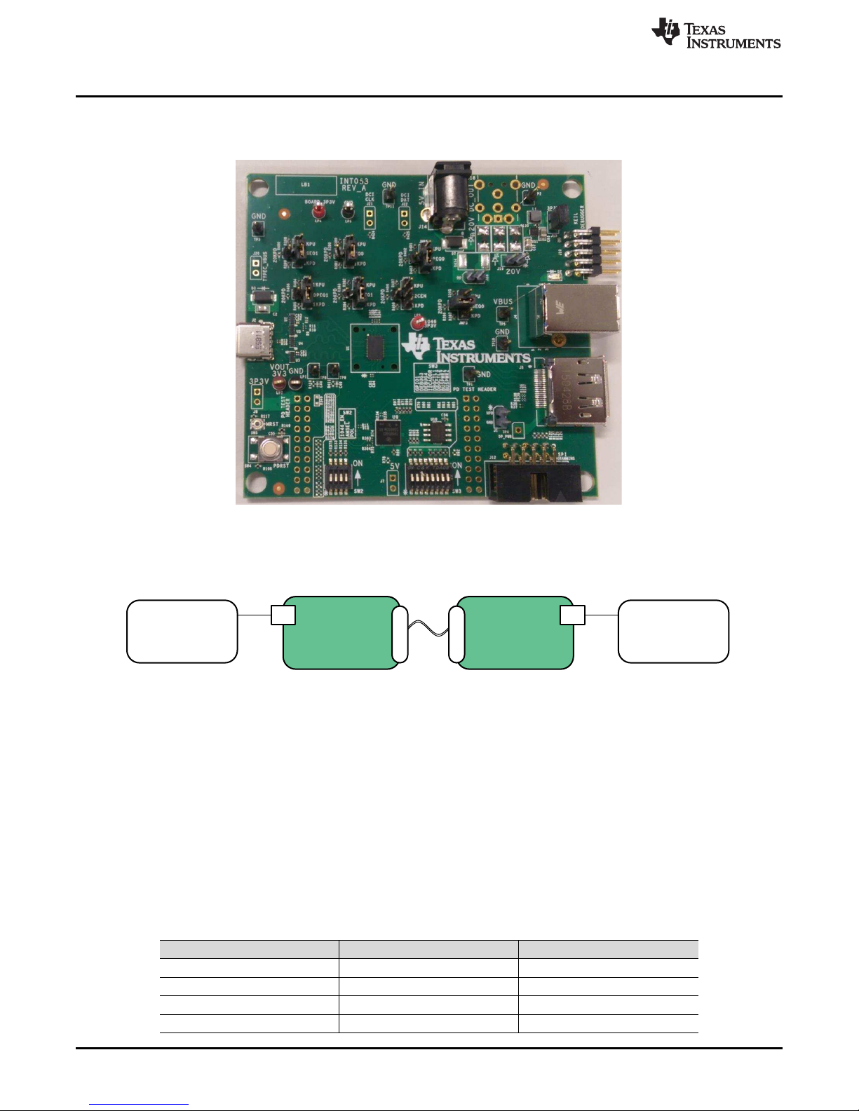
1 TUSB1042EVM
Figure 1 illustrates the EVM board.
www.ti.com
Figure 1. TUSB1042EVM
The TUSB1042EVM can be used with a legacy DP Source or USB Host system to evaluate the USB
Type-C implementation. Figure 2 is a typical test set-up.
Figure 2. Test Board Setup
The EVM comes with a legacy Type B USB receptacle to connect to USB host systems. The TUSB1042
EVM uses the Texas Instruments TPS65982 (http://www.ti.com/product/TPS65982/product) controller for
power delivery and CC pin control.
2 TUSB1042EVM Configuration
This section provides the configuration options available in the TUSB1042EVM.
2.1 TUSB1042 EVM Default EQ Configuration
The following headers are provided for TUSB1042 EQ configuration by default, configuration settings may
need to be optimized depending on the amount of loss of each channel in the system.
Table 1. TUSB1042 Configuration Pins
Reference Designator JMP Control Configuration
JMP1 Downstream EQ0 No Connect
JMP2 Downstream EQ1 Shunt on pin 2–4 (20K PD)
JMP3 Upstream SSEQ0 Shunt on pin 2–1 (1K PU)
JMP4 Upstream SSEQ1 Shunt on pin 2–4 (20K PD)
2
TUSB1042 Evaluation Module
Copyright © 2017, Texas Instruments Incorporated
SLLU277–September 2017
Submit Documentation Feedback
Page 3
www.ti.com
2.2 TUSB1042 EQ Control
Each of the TUSB1042 receiver lanes has individual controls for receiver equalization. Table 2 and
Table 3 detail the gain values for each available combination for downstream, upstream and all
DisplayPort™ configurations.
Level Settings
0 Option 1: Tie 1KΩ 5% to GND.
R Tie 20K Ω 5% to GND.
F Float (Leave pin open)
1 Option 1: Tie 1K Ω 5% to VCC.
USB 3.1 Downstream Facing Ports USB 3.1 Upstream Facing Ports
EQ1 Pin
Level
0 0 0 0 0 0
0 R 1 0 R 1
0 F 2 0 F 2
0 1 3 0 1 3
R 0 4 R 0 4
R R 5 R R 5
R F 6 R F 6
R 1 7 R 1 7
F 0 8 F 0 8
F R 9 F R 9
F F 10 F F 10
F 1 11 F 1 11
1 0 12 1 0 12
1 R 13 1 R 13
1 F 14 1 F 14
1 1 15 1 1 15
EQ0 Pin
Level
Table 2. Configuration Pin-Level Definitions
Option 2: Tie directly to GND.
Option 2: Tie directly to VCC.
Table 3. USB 3.1 EQ Settings
EQ Gain @ 5 GHz (dB) SSEQ1 Pin
Level
SSEQ0 Pin
Level
TUSB1042EVM Configuration
EQ Gain @ 5 GHz (dB)
2.3 Power
The EVM is designed to operate off of the VBUS from a USB host connected via USB Type B J4. No
external power to be applied via J14 unless standalone operation is desired.
If testing DisplayPort only, or if bypassing VBUS power, the EVM must be powered via J14 (5-V, 1-A
input).
SLLU277–September 2017
Submit Documentation Feedback
Copyright © 2017, Texas Instruments Incorporated
TUSB1042 Evaluation Module
3
Page 4
TUSB104 2
USB Type-B
Receptac le
USB-C(TM) Connector
TPS6598 2
3P3V
3P3V 5 V
SSTX
SSRX
C_SSTX1
C_SSTX2
C_SSRX1
C_SSRX2
Type_C VBUS
5V_IN
VBUS_5 V
5 V to 3.3 V
3.3 V
3.3 V
5 V
SBU
SBU
Copyright © 2017, Texas Instruments Incorporated
TUSB1042EVM Schematics
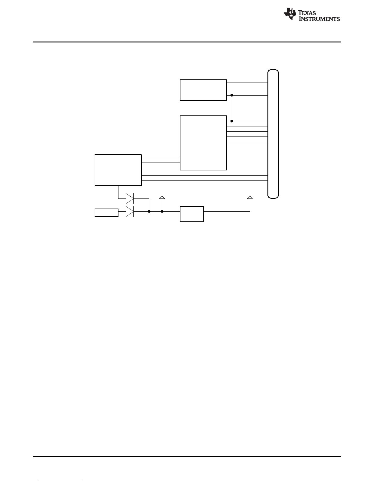
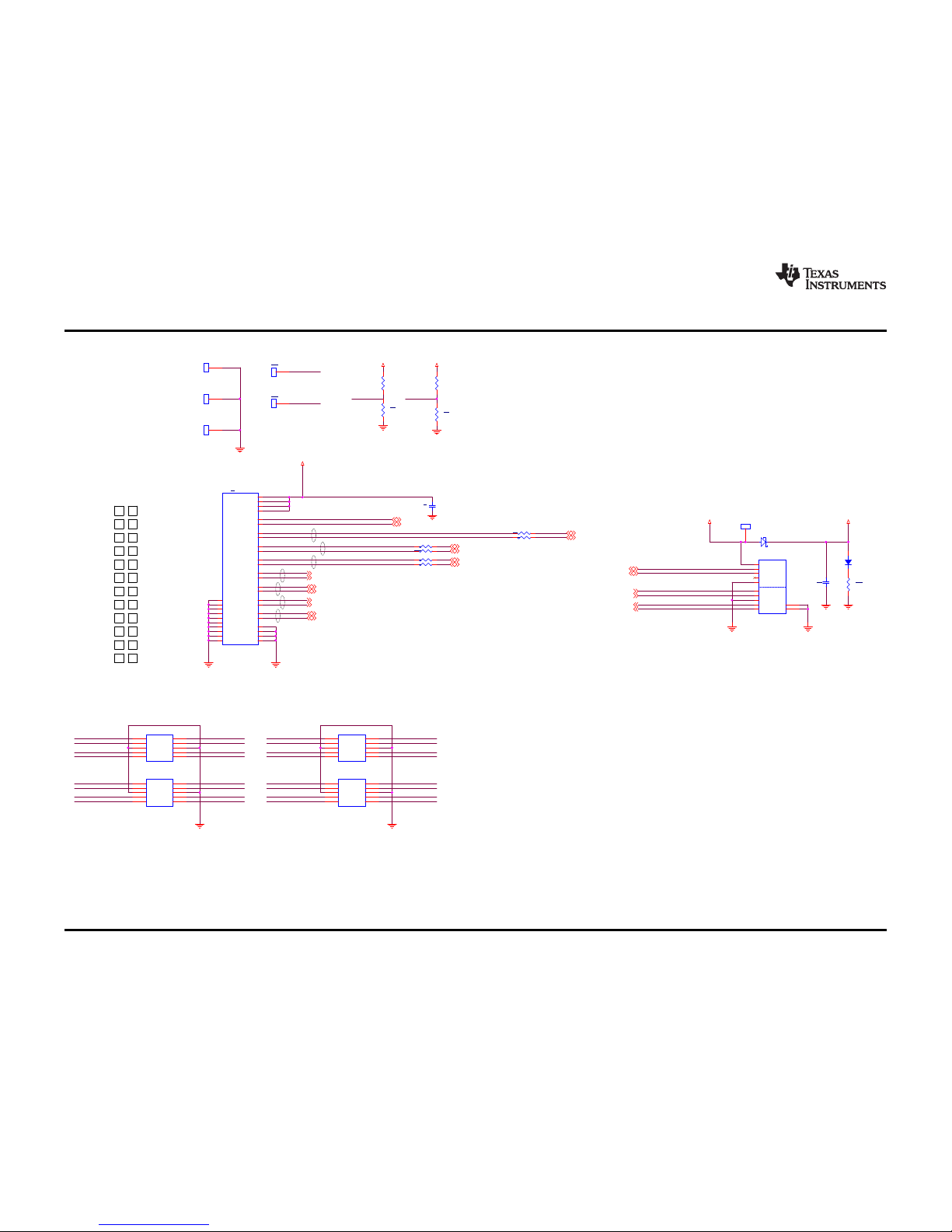
3 TUSB1042EVM Schematics
Figure 3 through Figure 7 illustrate the EVM schematics.
www.ti.com
Figure 3. TUSB1042EVM Block Diagram
4
TUSB1042 Evaluation Module
Copyright © 2017, Texas Instruments Incorporated
SLLU277–September 2017
Submit Documentation Feedback
Page 5

SILKSCREEN:
CTL0
POL/FLIP
1KPU
EQ0
SILKSCREEN
1KPD
20KPD
1KPU
EQ1
SILKSCREEN
1KPD
20KPD
1KPU
SSEQ0
SILKSCREEN
1KPD
20KPD
1KPU
SSEQ1
SILKSCREEN
1KPD
20KPD
1KPU
A1
SILKSCREEN
1KPD
20KPD
1KPU
20KPD
SILKSCREEN
1KPD
I2CEN
I2C_EN Header Config
1021_EQ* Config
1021_SSEQ* Config
SilkScreen:
Pad Sharing
TUSB1021
FLIP CTL0
X LOW POWER DOWN
POL Mux Operation
USB3.1 Orientation 1
USB3.1 Orientation 2
HIGH
HIGH
LOW
HIGH
Input from
TPS65982
1021_3P3V
SilkScreen:
BRD_3P3V
SilkScreen:
GND
Config Switch
SILKSCREEN
DCI_CLK
SILKSCREEN
DCI_DAT
TUSB1042 INT053A-002
Place R1 49 and R150 close to TUSB1021
CTL0
1021_EQ0
1021_I2C_EN
1021_EQ1
1021SSEQ0 1021SSEQ1
A1
CRX1N
CRX1P
CRX2P
CRX2N
DCI_DAT
I2C_SCL1021
I2C_SCL_Ext
POL
I2C_SDA1021
I2C_SDA_Ext
CTL0
1021SSEQ1
1021_EQ0
1021_EQ1
A1
1021_I2C_EN
1021SSEQ0
CTX2P_C
CTX2N_C
CTX1P_C
CTX1N_C
CTX2N
CTX2P
CTX1P
CTX1N
DCI_CLK
POL
1021_3P3V
BOARD_3P3V BOARD_3P3V
BOARD_3P3V BOARD_3P3V
BOARD_3P3V
BOARD_3P3V
LDO_1V8D
1021_3P3V
1021_3P3V
1021_3P3V
BOARD_3P3V
1021_3P3V
SSRXP_UP pg3
SSRXM_UP pg3
SSTXP_UP pg3
SSTXM_UP pg3
I2C_SCL_Ext pg4
POLpg3,4
I2C_SDA_Ext pg4
I2C_SDA1021 pg4
I2C_SCL1021 pg4
CRX2P pg3
CRX2N pg3
CRX1N pg3
CRX1P pg3
CTX2P pg3
CTX2N pg3
CTX1N pg3
CTX1P pg3
CTL0pg4
R116
1K +/- 5%
LP5
R156 0
R113 NC, 0
R153
NC,4.7K
LP3
C32 0.1uF
0201
JMP5
4 Pin-TBerg Jumper
1
234
C26
0.1uF
R155 NC, 0
SW1
SW DIP-2
R73
0
JMP1
4 Pin-TBerg Jumper
1
234
C33 0.1uF
0201
C28 0.1uF
0201
C34
10uF
R149 22
JMP7
4 Pin-TBerg Jumper
1
234
FB4
220 @ 100MHZ
R18
NC,10K
C29 0.1uF
0201
R132
1K +/- 5%
C27
0.1uF
R74
0
R127
20K +/- 5%
R117
1K +/- 5%
R125
20K +/- 5%
R123
1K +/- 5%
R150 22
R121
20K +/- 5%
R120
1K +/- 5%
LP4
C30 0.1uF
0201
R104 0
R124
1K +/- 5%
J16
NC, HEADER 2
1
2
C35
0.1uF
R134
1K +/- 5%
C31 0.1uF
0201
R119
1K +/- 5%
J17
NC, HEADER 2
1
2
R122
1K +/- 5%
C36
0.1uF
R126
1K +/- 5%
R114
1K +/- 5%
R17
4.7K
JMP2
4 Pin-TBerg Jumper
1
234
JMP3
4 Pin-TBerg Jumper
1
234
JMP4
4 Pin-TBerg Jumper
1
234
R151
NC,10K
TUSB1042
U9
RSVD1
RSVD2
SSEQ0_A0
RSVD3
RSVD4
A1
RSVD5
RSVD6
I2C_EN
RSVD7
RSVD8
VCC
DCI_DAT
RX1P
RX1N
DCI_CLK
TX1P
TX1N
EQ1
TX2N
TX2P
EQ0
RX2N
RX2P
GND
VCC
TEST2
SSEQ1
SSRXN
SSRXP
VCC
SSTXN
SSTXP
FLIP_SCL
CTL0_SDA
TEST1
RSVD9
RSVD10
RSVD11
RSVD12
VCC
R115
20K +/- 5%
R128
1K +/- 5%
R118
20K +/- 5%
R133
20K +/- 5%
Copyright © 2017, Texas Instruments Incorporated
www.ti.com
TUSB1042EVM Schematics
5
SLLU277– September 2017
Submit Documentation Feedback
Copyright © 2017, Texas Instruments Incorporated
TUSB1042 Evaluation Module
Figure 4. TUSB1042EVM (Schematic 1 of 4)
Page 6
A10
VBUS
GND
A11
A12
SSRXP1
SSRXP2
SSRXN1
SSRXN2
B9
B8
B7
B6
B5
B4
B3
B2
B1
DN2
SBU2
GND
VBUS
B12
B11
B10
CC1
GND
DP1
DN1
SBU1
VBUS
SSTXP1
SSTXP2
SSTXN1
SSTXN2
SSRXP2
SSRXP1
SSRXN2
SSRXN1
DP2
SSTXP2
SSTXP1
SSTXN2
SSTXN1
GND
VBUS
CC2
TypeC Connector and Source
Pin Mapping
A1
A2
A3
A4
A5
A6
A7
A8
A9
Test Purpose
Headers and
Options
place near J2 Type-C connector
SILKSCREEN
GND
GND
GND
ESD
Components
SILKSCREEN:
5V_IN
USB Host
Connecti on
USB and DP Connectors
TUSB1042 INT053A-002
CSBU1
CSBU2
C_CC1C_CC2
CTX1N
CTX1P
CRX1N
CRX1P
C_CC1
C_CC2
CSBU1
CSBU2
C_CC1
C_CC2
CSBU1
CSBU2
CTX1N
CTX1P
CRX1N
CRX1P
C_T_DM
C_T_DP
C_B_DP
C_B_DM
CRX2P
CRX2N
CTX2N
CTX2P
CTX2N
CTX2P
CRX2N
CRX2P
C_USB_TN
C_USB_TP
C_USB_BP
C_USB_BN
C_USB_TN
C_USB_TP
C_USB_BN
C_USB_BP
5V_COM
C_CC2
C_CC1
SSTXM_UP
SSTXP_UP
SSRXM_UP
SSRXP_UP
BOARD_3P3V BOARD_3P3V
TypeC_VBUS
5V_COMVBUS_TYPEB
C_CC1 pg4
C_CC2 pg4
CSBU1_65982 pg4
CSBU2_65982 pg4
C_USB_TP pg4
C_USB_TN pg4
C_USB_BP pg4
C_USB_BN pg4
CTX2P pg2
CTX2N pg2
CTX1N pg2
CTX1P pg2
CRX2P pg2
CRX2N pg2
CRX1N pg2
CRX1P pg2
DM_UPpg4
DP_UPpg4
SSTXM_UPpg2
SSTXP_UPpg2
SSRXM_UPpg2
SSRXP_UPpg2
R4
NC, 10K
D2
LED Green 0805
D1
PMEG3050EP, 115
12
U2
TPD4E05U06
D1+
1
D1-
2
GND
3
D2+
4
D2-5NC6
6
NC7
7
GND
8
NC9
9
NC10
10
R1
NC, 10K
R25
330
0402
5%
USB2
USB3
J1
USB3_MICRO_B
VBUS
1
D-
2
D+
3
USB_OTG
4
GND
5
TX-
6
TX+
7
GND1
8
RX-
9
RX+
10
SLD1
11
SLD2
12
TP1
TEST POINT
1
J2
TypeC_Receptacle_DualSMT_TOP
GND0
A1
SSTXP1
A2
SSTXN1
A3
VBUS1
A4
CC1
A5
DP1
A6
DN1
A7
SBU1
A8
VBUS2
A9
SSRXN2
A10
SSRXP2
A11
GND1
A12
GND2
B1
SSTXP2
B2
SSTXN2
B3
VBUS3
B4
CC2
B5
DP2
B6
DN2
B7
SBU2
B8
VBUS4
B9
SSRXN1
B10
SSRXP1
B11
GND3
B12
Shield1
1
Shield2
2
Shield3
3
Shield4
4
Shield5
5
Shield6
6
Shield8
8
Shield7
7
Shield10
10
Shield9
9
U5
TPD4E05U06
D1+
1
D1-
2
GND
3
D2+
4
D2-5NC6
6
NC7
7
GND
8
NC9
9
NC10
10
TP6
TEST POINT
1
C2
10uF
R7 0
U3
TPD4E05U06
D1+
1
D1-
2
GND
3
D2+
4
D2-5NC6
6
NC7
7
GND
8
NC9
9
NC10
10
TP5
TEST POINT
1
TP7
TEST POINT
1
R10 0
R15 0
R2
NC, 1M
U4
TPD4E05U06
D1+
1
D1-
2
GND
3
D2+
4
D2-5NC6
6
NC7
7
GND
8
NC9
9
NC10
10
TP2
TEST POINT
1
C1
10uF
R16 0
TP3
TEST POINT
1
R12 0
R5
NC, 1M
R11 0
Copyright © 2017, Texas Instruments Incorporated
TUSB1042EVM Schematics
www.ti.com
6
SLLU277– September 2017
Submit Documentation Feedback
Copyright © 2017, Texas Instruments Incorporated
TUSB1042 Evaluation Module
Figure 5. TUSB1042EVM (Schematic 2 of 4)
Page 7

GND
982_3V3
TPS65982
PD
Controller
NOTE: OPEN by default
PDCTRL
SILKSCREEN:
GPIO1
DEBUG3
DEBUG4
I2CADDR
DBGCTL1
DBGCTL2
BUSPWRz
SILKSCREEN:
SILKSCREEN: PD Test Headers
P
ad Sharing
SILKSCREEN: PD Test Headers
SILKSCREEN:
SILKSCREEN:
PDRST
MRST
Place near the edge
Keil
Debugger
Header
SPI
Programming
Header
SILKSCREEN:
SPI
NOTE:ALL DIFF PAIRS ARE
ROUTED85 TO 90 OHMS
DIFFERENTIALAND 50 OHMS
COMMONMODE. ALL OTHER
TRACESARE 50 OHM.
Pad Sharing
TUSB1042 INT053A-002
17309_D
HV_GATE1
HV_GATE2
17309_S
65982_VBUS
GPIO0
GPIO1
GPIO2
GPIO3
GPIO6
GPIO7
GPIO8
LDO_1V8A
LDO_BMC
DEBUG1
DEBUG2
DEBUG4
DEBUG3
LSX_R2P
LSX_P2R
SPI_MOSI
SPI_CLK
SPI_SSZ
SPI_MISO
SWD_CLK
SWD_DAT
UART_RX
UART_TX
I2C_SCL1
I2C_SDA1
I2C_ADDR
I2C_IRQ1Z
I2C_SCL2
I2C_SDA2
I2C_IRQ2Z
PD_RESETZ
PD_MRESET
PD_BUSPWRZ
SPI_SSZ
SPI_MISO
SPI_MOSI
SPI_CLK
SPI_HOLD#
SPI_WP#
PD_SYS_RST
I2C_ADDR
GPIO1
DEBUG3
DEBUG4
DBG_CTL1
DBG_CTL2
PD_BUSPWRZ
GPIO1_H
DEBUG3_H
DEBUG4_H
DBG_CTL1_H
DBG_CTL2_H
PD_BUSPWRZ_3V3
PD_BUSPWRZ_1V8
982_CC1
982_CC2
J15.8
PD_RESETZ
J15.10
I2C_SCL1
SPI_SSZ
SWD_DAT
SWD_CLK
SWD_DAT
DEBUG2
DEBUG4
DBG_CTL2
GPIO0
LSX_P2R
LSX_R2P
J15_1
J15_3
GPIO6_8
DEBUG1
DEBUG3
PD_MRESET
GPIO8
GPIO6
SPI_MISO
SPI_MOSI
I2C_IRQ1Z
SPI_SSZ
DEBUG1_3
DEBUG2_4
I2C_SCL2
I2C_SDA2
I2C_SCL1021
I2C_SDA1021
I2C_SCL1
I2C_SDA1
UART_RX
UART_TX
I2C_SDA1
I2C_IRQ2Z
J17_11
J17_13
I2C_SCL2
I2C_SDA2
I2C_SCL1
I2C_SDA1
J17_17
PD_SYS_RST
PD_MRESET
SWD_CLK
SWD_DAT
I2C_SCL2
I2C_SDA2
I2C_SCL1
I2C_SDA1
SPI_MISO
SPI_CLK SPI_MOSI
SPI_SSZ
GPIO1
GPIO2
GPIO0
I2C_SCL_Ext
I2C_SDA_Ext
GPIO1
SPI_CLK
J17_13
J17_20
CTL0
J17_12
J17_14
GPIO7
GPIO3
J17_12
J17_14
J17_16
SPI_MISO
SPI_MOSI
J17_10
J17_16 DBG_CTL1
POL
J17_10
GPIO2
J17_11
I2C_SCL1021
I2C_SDA1021
DBG_CTL1
DBG_CTL2
DBG_CTL1_R
DBG_CTL2_R
BOARD_3P3V
LDO_3V3
LDO_3V3LDO_3V3
LDO_1V8D
LDO_3V3
VOUT_3V3
BOARD_12V
BOARD_20V
65982_5V
65982_3P3V
TypeC_VBUS
LDO_1V8D
LDO_3V3
5V_COM
BOARD_20V
BOARD_12V
5V_COM
SYS_DC_OUT
5V_COM LPad_5V
LPad_3P3V
BOARD_3P3V
BOARD_3P3V
65982_3P3V
BOARD_3P3V
TypeC_VBUS
LPad_5V LPad_5VLPad_3P3V
C_USB_TP pg3
C_USB_TN pg3
C_USB_BP pg3
C_USB_BN pg3
CSBU1_65982 pg3
CSBU2_65982 pg3
C_CC1 pg3,4
C_CC2 pg3,4
DP_UPpg3
DM_UPpg3
I2C_SCL1021pg2
I2C_SDA1021pg2
POL pg2,3
CTL0 pg2
1021_EN pg2
I2C_SCL_Extpg2
I2C_SDA_Extpg2
C_CC1 pg3,4
C_CC2 pg3,4
C8
0.1uF
R136 NC, 0
R67 0
R32
NC, 0
R62 3.3K
R90 NC, 0
C20
1uF
R42
1K
D5
PMEG3050EP, 115
12
R109 0
C22
0.01uF
R13 0
C14
1uF
R36 15K
R94 0
R40
1K
R101 NC, 0
R146 NC, 0
R85 NC, 0
R68 0
LP1
D6
DNI, PMEG3050EP, 115
12
R46
100K
R110 0
C11
0.01uF
R65
100K
R158 NC, 0
R82 NC, 0
R14 0
J7
Header 5x2 0.1" RAthru-hole
2
4
6
8
10
1
3
5
7
9
R44
1K
R81
NC, 0R
R97 NC, 0
R87 NC, 0
R160 0
R86 NC, 0
J6
NC, HEADER 2
1
2
R39
1K
R111 0
D3
B340A-13-F
R159 NC, 0
R95 0
C9
0.01uF
R50
100K
C3
10uF
R141 NC, 0
R161 0
R157
NC, 0R
R66
1K
R43
1K
LP2
R26
0.01, 1%, 0.25W
R35 0
R96 0
R143 0
TP8
TESTPOINT
1
TP9
TESTPOINT
1
R142 NC, 0
R88 NC, 0
R112 0
C5
10uF
R57
3.3K
U7
W25Q80
/CS
1
DO
2
/WP
3
GND
4
VCC
8
CLK
6
DI
5
/HOLD
7
C10
0.01uF
J5
NC, HEADER 2
1
2
R45
1K
J12
NC, HDR10x2 M .1 Receptacle
3
1 2
4
5 6
7 8
9 10
11 12
13 14
15 16
17 18
19 20
R98 NC, 0
SW4
SWITCH SPST-NO
14
23
R91 NC, 0
R138 0
FB3
21 @ 100MHZ
C21
0.01uF
J18
1
2
R144 0
R47
100K
R99 0
SW3
B3SN-3012
1 4
2 3
C17
10uF
C15
220pF
R28
0
CSD17309Q3
Q1
4
3
2
1 8
7
6
5
9
R58
3.3K
R59 3.3K
J15
NC, HEADER 2
1
2
J8
Header 5x2 0.1" Shroud RAthru-hole
2
4
6
8
10
1
3
5
7
9
R92 0
R147 0
R31 0
R53
10K
R60 3.3K
R54
3.3K
C18
1uF
C13
10uF
R63 3.3K
R55
3.3K
R56
10K
C19
1uF
R41
1K
R29 0
FB1
21 @ 100MHZ
R89 0
SW2
8-POS 50-MILSMT
1
2
3
4
5
6
7
8
16
15
14
13
12
11
10
9
C12
0.01uFR34 0
R70 0
C6
0.1uF
C4
0.22uF
R33
NC, 0
R139 0
CSD17309Q3
Q2
4
3
2187
6
5
9
R61 NC, 3.3K
R51
100K
R30 0
R100 NC, 0
J14
1
2
C7
22uF
R48
100K
R64
1K
J11
NC, HDR10x2 M .1 Receptacle
3
1 2
4
5 6
7 8
9 10
11 12
13 14
15 16
17 18
19 20
R83 NC, 0
R69 0
R135 NC, 0
R27
0
C16
220pF
R93 0
FB2
220 @ 100MHZ
R140 0
R52
NC,TBD
U6
TPS65982
GND
A1
LDO_1V8D
A2
SPI_CLK
A3
SPI_MISO
A4
I2C_SDA2
A5
PP_HV1
A6
PP_HV2
A7
PP_HV3
A8
HV_GATE2
A9
SENSEN
A10
PP_5V0_2
A11
VDDIO
B1
GPIO0
B2
SPI_SSZ
B3
SPI_MOSI
B4
I2C_SCL2
B5
I2C_IRQ2Z
B6
PP_HV4
B7
GND
B8
HV_GATE1
B9
SENSEP
B10
PP_5V0_1
B11
I2C_IRQ1Z
C1
GPIO1
C2
GPIO4
C10
PP_5V0_3
C11
I2C_SDA1
D1
I2C_SCL1
D2
DBG_CTL2
D5
HRESET
D6
GPIO7
D7
GND
D8
GPIO2
D10
PP_5V0_4
D11
LDO_BMC
E1
UART_TX
E2
DBG_CTL1
E4
GNDE5GNDE6GNDE7GND
E8
GPIO5
E10
MRESET
E11
I2C_ADDR
F1
UART_RX
F2
SWD_DAT
F4
GNDF5GNDF6GNDF7GND
F8
BUSPOWERZ
F10
RESETZ
F11
LDO_3V3
G1
R_OSC
G2
SWD_CLK
G4
GNDG5GNDG6GNDG7GND
G8
GPIO6
G10
GPIO3
G11
VIN_3V3
H1
VOUT_3V3
H2
GNDH4GND
H5
GPIO8
H6
SS
H7
GND
H8
PP_CABLE
H10
VBUS1
H11
AUX_P
J1
AUX_N
J2
VBUS2
J10
VBUS3
J11
LDO_1V8A
K1
DEBUG2
K2
DEBUG4
K3
LSX_P2R
K4
USB_RP_N
K5
C_USB_TP
K6
C_USB_BP
K7
C_SBU1
K8
RPD_G1
K9
RPD_G2
K10
VBUS4
K11
GND
L1
DEBUG1
L2
DEBUG3
L3
LSX_R2P
L4
USB_RP_P
L5
C_USB_TN
L6
C_USB_BN
L7
C_SBU2
L8
C_CC1
L9
C_CC2
L10
NC
L11
D4
PMEG3050EP, 115
12
R145 0
R49
100K
R84 NC, 0
Copyright © 2017, Texas Instruments Incorporated
www.ti.com
TUSB1042EVM Schematics
7
SLLU277– September 2017
Submit Documentation Feedback
Copyright © 2017, Texas Instruments Incorporated
TUSB1042 Evaluation Module
Figure 6. TUSB1042EVM (Schematic 3 of 4)
Page 8

NOTE: POPULATE JUMPER BY DEFAULT
20V DC_OUT
SILKSCREEN:
SILKSCREEN:
5V_IN
5V DC Input
TUSB1042 INT053A-002
U3_SW
U3_PG
5V_IN
BOARD_3P3V
5V_COM
SYS_DC_OUT
5V_COM
J9
1
2
R71
178K
C24
10uF
J10
DC_POWER_JACK
1
2
3
C23
10uF
J13
JPD1135-509-7F
POWER1
2
SENSE
1
POWER2
3
GND1
4
GND2
5
SHIELD1
6
SHIELD2
7
SHIELD3
8
SHIELD4
9
L1
1uH
C25
22uF
D7
PMEG3050EP, 115
1
2
U8
TPS62082DSGT
VIN
8
EN
1
MODE
3
GND
2
PwPd
9
FB
4
VOS
5
SW
7
PG
6
Copyright © 2017, Texas Instruments Incorporated
TUSB1042EVM Schematics
www.ti.com
8
SLLU277– September 2017
Submit Documentation Feedback
Copyright © 2017, Texas Instruments Incorporated
TUSB1042 Evaluation Module
Figure 7. TUSB1042EVM (Schematic 4 of 4)
Page 9

www.ti.com
Bill of Materials
9
SLLU277– September 2017
Submit Documentation Feedback
Copyright © 2017, Texas Instruments Incorporated
TUSB1042 Evaluation Module
4 Bill of Materials
Table 4 lists the TUSB1042EVM bill of materials (BOM).
Table 4. TUSB1042EVM Bill of Materials
Item Qty Reference Part PCB Footprint Manufacturer Manufacturer Part Number Description
1 6 C1,C2,C3,C23,C24,C34 10uF 805 Murata GRM21BR61C106KE15K CAP CER 10UF 16V X5R 0805
2 1 C4 0.22uF 402 Murata GRM152R61A224KE19D CAP CER 0.22UF 10V X5R 0402
3 2 C5,C17 10uF 603 Murata GRM188R61C106MA73D CAP CER 10UF 16V X5R 0603
4 2 C6,C8 0.1uF 402 Murata GRM155R61A104KA01D CAP CER 0.1UF 10V X5R 0402
5 1 C7 22uF 603 Murata GRM188R60J226MEA0D CAP CER 22UF 6.3V X5R 0603
6 6 C9,C10,C11,C12,C21,C22 0.01uF 402 Murata GRM155R71C103KA01D CAP CER 10000PF 16V X7R 0402
7 1 C13 10uF 402 Samsung CL05A106MP8NUB8 CAP CER 10UF 10V X5R 0402
8 1 C14 1uF 603 Murata GRM188R61C105KA93D CAP CER 1UF 16V X5R 0603
9 2 C15,C16 220pF 402 Murata GRM1555C1H221JA01D CAP CER 220PF 50V NP0 0402
10 3 C18,C19,C20 1uF 402 Murata GRM155R60J105ME19D CAP CER 1UF 6.3V X5R 0402
11 1 C25 22uF 805 Samsung CL21A226MOCLRNC CAP CER 22UF 16V X5R 0805
12 10 C26,C27,C28,C29,C30,C31,C32,C3
3,C35,C36
0.1uF 201 Murata GRM033R61C104KE84D CAP CER 0.1UF 16V X5R 0201
13 4 D1,D4,D5,D6 SCHOTTKY diode_smb NXP PMEG3050EP,115 DIODE SCHOTTKY 30V 5A SOD128
14 1 D2 LED Green 0805 805 Lumex SML-LX0805GC-TR LED GREEN CLEAR 0805 SMD
15 1 D3 B340A-13-F SMA Diodes Inc B340A-13-F DIODE SCHOTTKY 40V 3A SMA
16 1 D7 SCHOTTKY DO-214AA NXP PMEG3050EP,115 DIODE SCHOTTKY 30V 5A SOD128
17 2 FB1,FB3 21 @ 100MHZ 805 Taiyo Yuden FBMJ2125HM210NT FERRITE BEAD 21 OHM 0805 1LN
18 2 FB2,FB4 220 @ 100MHZ 603 Murata BLM18EG221SN1D FERRITE BEAD 220 OHM 0603 1LN
19 6 JMP1,JMP2,JMP3,JMP4,JMP5,JMP74 Pin-T Berg Jumper berg2x3tee Samtec HTSW-150-08-G-S CONN HEADER 50POS .100" T/H GOLD
20 0 JMP6 DNI - 4 Pin-T Berg
Jumper
berg2x3tee Samtec HTSW-150-08-G-S CONN HEADER 50POS .100" T/H GOLD
21 3 J1,J14,J18 CON02 HDR_THVT_1X2_100_MFCI 68001-402HLF BERGSTIK II .100" SR STRAIGHT
22 1 J2 TypeC_Receptacle_Dual
SMT_TOP
USB_TYPEC_UT1211 Foxconn UT12113-11601-7H USB Type C Surface Mount Connector
23 0 J3 DNI- DP SINK-SIDE
CONNECTOR
con_DP_SD-47272001
Molex Inc 472720001 DisplayPort Receptacle Connector 20 Position Surface Mount, Right Angle,
Horizontal
24 1 J4 USB3_TYPEB_CONNEC
TOR
usb3_typeb_ak4aa009 Amphenol Commercial
Products
GSB4211311WEU USB - B USB 3.1, Superspeed+ Receptacle Connector 9 Position Through
Hole, Right Angle
25 0 J5,J6,J15,J16,J17 NC,HEADER 2 berg1x2 Omron Electronics Inc-EMC
Div
XG8T-0231 JUMPERPLUG 2POS DOUBLE ROW
26 1 J7 Header5x2 0.1" RA thru-
hole
HDR_THRT_68020 Amphenol FCI 68021-210HLF CONN HEADER 10POS .100 R/A 15AU
27 1 J8 Header5x2 0.1" Shroud
RA thru-hole
HDR_THRT_2X5_100 Amphenol FCI 67997-410HLF CONN HEADER 10POS .100 STR TIN
28 1 J9 CON02 berg1x2 FCI 68001-402HLF BERGSTIK II .100" SR STRAIGHT
29 1 J10 DC_PWR_JACK pj-202ah CUI Inc. PJ-202AH CONN PWR JACK 2.0X6.5MM HIGH CUR
30 0 J11,J12 NC, HDR10x2 M .1
Receptacle
HDR_THVT_2x10_100_FSullins Connector Solutions PPPC102LFBN-RC 20 Position Header Connector 0.100" (2.54mm) Through Hole Gold
Page 10

Bill of Materials
www.ti.com
10
SLLU277– September 2017
Submit Documentation Feedback
Copyright © 2017, Texas Instruments Incorporated
TUSB1042 Evaluation Module
Table 4. TUSB1042EVM Bill of Materials (continued)
Item Qty Reference Part PCB Footprint Manufacturer Manufacturer Part Number Description
31 1 J13 JPD1135-509-7F Jack_THRT_JPD1135 Foxconn JPD1135-509-7F DCPOWER PLUG OR JACK
32 2 LP1,LP5 LP tp_thvt_060_rnd Keystone Electronics 5011 TEST POINT PC MULTI PURPOSE BLK
33 3 LP2,LP3,LP4, LP tp_thvt_060_rnd Keystone Electronics 5010 TEST POINT PC MULTI PURPOSE BLK
34 1 L1 1uH IND_NR3015 Taiyo Yuden NR3015T1R0N FIXED IND 1UH 2.1A 36 MOHM SMD
35 2 Q1,Q2 MOS_P_4D_3S Q3_SON-8 Texas Instruments CSD17309Q3 MOSFET N-CH 30V 60A 8SON
36 0 R1,R4 NC, 10K 402 Panasonic Electronic
Components
ERJ-2GEJ103X RES SMD 10K OHM 5% 1/10W 0402
37 0 R2,R5 NC, 1M 402 PanasonicElectronic
Components
ERJ-2GEJ105X RES SMD 1M OHM 5% 1/10W 0402
38 0 R3,R6,R31,R32,R33,R38,R83,R84,
R85,R86,R90,R91,R100,R101,R11
3,R135,R136,R141,R142,R146,R14
8,R155,R158,R159
NC, 0 402 Panasonic Electronic
Components
ERJ-2GE0R00X RES SMD 0.0OHM JUMPER 1/10W 0402
39 0 R7,R10,R79,R80,R87,R88,R97,R98
,R105,R106,R107,R108
NC, 0 201 Panasonic Electronic
Components
ERJ-1GN0R00C RES SMD 0.0OHM JUMPER 1/20W 0201
40 16 R8,R9,R11,R12,R13,R14,R15,R16,
R34,R35,R94,R95,R96,R99,R109,R
110
0 201 Panasonic Electronic
Components
ERJ-1GN0R00C RES SMD 0.0OHM JUMPER 1/20W 0201
41 2 R17,R19 4.7K 402 Panasonic Electronic
Components
ERJ-2GEJ472X RES SMD 4.7K OHM 5% 1/10W 0402
42 0 R18,R103,R151 NC,10K 402 Panasonic Electronic
Components
ERJ-2GEJ103X RES SMD 10K OHM 5% 1/10W 0402
43 0 R20,R21 NC, 100k 402 Panasonic Electronic
Components
ERJ-2GEJ104X RES SMD 100K OHM 5% 1/10W 0402
44 0 R22,R23 DNI, 0 201 Panasonic Electronic
Components
ERJ-1GN0R00C RES SMD 0.0OHM JUMPER 1/20W 0201
45 0 R24 NC, 5M 201 PanasonicElectronic
Components
ERJ-1GEF1004C RESSMD 1M OHM 1% 1/20W 0201
46 1 R25 330 402 Panasonic Electronic
Components
ERJ-2GEJ331X RES SMD 330 OHM 5% 1/10W 0402
47 1 R26 0.01, 1%, 0.25W 805 Panasonic Electronic
Components
ERJ-6BWFR010V RES SMD 0.01 OHM 1% 1/2W 0805
48 32 R27,R28,R29,R30,R37,R67,R68,R6
9,R70,R72,R73,R74,R89,R92,R93,
R102,R104,R111,R112,R137,R138,
R139,R140,R143,R144,R145,R147,
R156,R160,R161,R164,R165
0 402 Panasonic Electronic
Components
ERJ-2GE0R00X RES SMD 0.0OHM JUMPER 1/10W 0402
49 1 R36 15K 402 PanasonicElectronic
Components
ERJ-2RKF1502X RES SMD 15K OHM 1% 1/10W 0402
50 21 R39,R40,R41,R42,R43,R44,R45,R6
4,R66,R114,R116,R117,R119,R120
,R122,R123,R124,R126,R128,R132
,R134
1K 402 Panasonic Electronic
Components
ERJ-2GEJ102X RES SMD 1K OHM 5% 1/10W 0402
51 7 R46,R47,R48,R49,R50,R51,R65 100K 402 Panasonic Electronic
Components
ERJ-2GEJ104X RES SMD 100K OHM 5% 1/10W 0402
52 0 R52 NC, 100 402 Panasonic Electronic
Components
ERJ-2GEJ101X RES SMD 100 OHM 5% 1/10W 0402
53 3 R53,R56,R154 10K 402 Panasonic Electronic
Components
ERJ-2GEJ103X RES SMD 10K OHM 5% 1/10W 0402
Page 11
www.ti.com
Bill of Materials
11
SLLU277– September 2017
Submit Documentation Feedback
Copyright © 2017, Texas Instruments Incorporated
TUSB1042 Evaluation Module
Table 4. TUSB1042EVM Bill of Materials (continued)
Item Qty Reference Part PCB Footprint Manufacturer Manufacturer Part Number Description
54 8 R54,R55,R57,R58,R59,R60,R62,R633.3K 402 Panasonic Electronic
Components
ERJ-2GEJ332X RES SMD 3.3K OHM 5% 1/10W 0402
55 0 R61 NC, 3.3K 402 Panasonic Electronic
Components
ERJ-2GEJ332X RES SMD 3.3K OHM 5% 1/10W 0402
56 1 R71 178K 402 Yageo RC0402FR-07178KL RES SMD 178K OHM 1% 1/16W 0402
57 0 R75,R76,R77,R78 NC, 1M 201 Panasonic Electronic
Components
ERJ-1GEF1004C RESSMD 1M OHM 1% 1/20W 0201
58 0 R81,R157 NC, 0R 2512 Vishay Dale RCL12250000Z0EG RES SMD 0.0 OHM 2W 2512 WIDE
59 0 R82 NC, 0 603 Yageo RC0603JR-070RL RESSMD 0.0OHM JUMPER 1/10W 0603
60 6 R115,R118,R121,R125,R127,R133 20K 402 Panasonic Electronic
Components
ERJ-2GEJ203X RES SMD 20K OHM 5% 1/10W 0402
61 0 R129,R130 DNI - 1K 402 Panasonic Electronic
Components
ERJ-2GEJ102X RES SMD 1K OHM 5% 1/10W 0402
62 0 R131 DNI - 20K 402 Panasonic Electronic
Components
ERJ-2GEJ203X RES SMD 20K OHM 5% 1/10W 0402
63 0 R149,R150 DNI, 20 402 Panasonic Electronic
Components
ERJ-2GEJ200X RES SMD 20 OHM 5% 1/10W 0402
64 0 R152,R153 NC,4.7K 402 Panasonic Electronic
Components
ERJ-2GEJ472X RES SMD 4.7K OHM 5% 1/10W 0402
65 0 R162 DNI, 0 402 Panasonic Electronic
Components
ERJ-2GE0R00X RES SMD 0.0OHM JUMPER 1/10W 0402
66 0 R163 DNI - 0 402 Panasonic Electronic
Components
ERJ-2GE0R00X RES SMD 0.0OHM JUMPER 1/10W 0402
67 1 SW1 4-POS 50-MIL SMT sw_smvt_dip_4pos_8 C&K(ITT-CANNON) TDA04H0SB1R SWITCH DIP 4POS HALF PITCH 24V
68 1 SW2 8-POS 50-MIL SMT SW_SMVT_SPST_TD
A08
C&K(ITT-CANNON) TDA08H0SB1R SWITCH DIP 8POS HALF PITCH 24V
69 1 SW3 B3SN-3012 switch_b3sn Omron Electronics Inc-EMC
Div
B3SN-3012P SWITCH TACTILE SPST-NO 0.05A 24V
70 1 SW4 SWITCH SPST-NO kmt2_switch C&K Components KMT221GHF LFS SWITCH TACTILE SPST-NO 0.05A 32V
71 8 TP1,TP2,TP3,TP5,TP6,TP7,TP8,TP9TEST POINT berg1x1 Samtec HTSW-101-07-G-S CONN HEADER 1POS .100" SGL GOLD
72 0 TP4 NC, TEST POINT berg1x1 Keystone Electronics 1035 TERM TEST POINT SLOTTED .060"DIA
73 1 U1 TUSB1042 SKT_IRONWOOD_C1
4861_QFN-40
Texas Instruments TUSB1042RNQR VESA USB Type-C Alt Mode redriving switch supporting data rates up to 10
Gbps for down facing port (Host).
74 4 U2,U3,U4,U5 TPD4E05U06 DQA Texas Instruments TPD4E05U06DQAR TVS DIODE 5.5VWM 14VC 10SON
75 1 U6 TPS65982 ZQZ_BGA_96 Texas Instruments TPS65982ABZQZR IC PWR MGMT CONV 3LDO 96BGA
76 1 U7 W25Q80 SOIC_8_197x157_50 WINBOND W25Q80DVSNIG IC FLASH 8MBIT 104MHZ 8SOIC
77 1 U8 TPS62082DSGT dsg Texas Instruments TPS62082DSGT IC REG BUCK 3.3V 1.2A SYNC 8WSON
78 5 SHUNT Sullins Connector Solutions SPC02SYAN Place set as Table 1.
79 1 LB1 TUSB1042EVM INT053-
002
PCB Label 0.650"H x
0.200"W
Texas Instruments THT-14-423-10 Thermal Transfer Printable Labels, 0.650" W x 0.200" H - 10,000 per roll
80 1 PCB ANY INT053 Printed Circuit Board.
Page 12

STANDARD TERMS FOR EVALUATION MODULES
1. Delivery: TI delivers TI evaluation boards, kits, or modules, including any accompanying demonstration software, components, and/or
documentation which may be provided together or separately (collectively, an “EVM” or “EVMs”) to the User (“User”) in accordance
with the terms set forth herein. User's acceptance of the EVM is expressly subject to the following terms.
1.1 EVMs are intended solely for product or software developers for use in a research and development setting to facilitate feasibility
evaluation, experimentation, or scientific analysis of TI semiconductors products. EVMs have no direct function and are not
finished products. EVMs shall not be directly or indirectly assembled as a part or subassembly in any finished product. For
clarification, any software or software tools provided with the EVM (“Software”) shall not be subject to the terms and conditions
set forth herein but rather shall be subject to the applicable terms that accompany such Software
1.2 EVMs are not intended for consumer or household use. EVMs may not be sold, sublicensed, leased, rented, loaned, assigned,
or otherwise distributed for commercial purposes by Users, in whole or in part, or used in any finished product or production
system.
2 Limited Warranty and Related Remedies/Disclaimers:
2.1 These terms do not apply to Software. The warranty, if any, for Software is covered in the applicable Software License
Agreement.
2.2 TI warrants that the TI EVM will conform to TI's published specifications for ninety (90) days after the date TI delivers such EVM
to User. Notwithstanding the foregoing, TI shall not be liable for a nonconforming EVM if (a) the nonconformity was caused by
neglect, misuse or mistreatment by an entity other than TI, including improper installation or testing, or for any EVMs that have
been altered or modified in any way by an entity other than TI, (b) the nonconformity resulted from User's design, specifications
or instructions for such EVMs or improper system design, or (c) User has not paid on time. Testing and other quality control
techniques are used to the extent TI deems necessary. TI does not test all parameters of each EVM.
User's claims against TI under this Section 2 are void if User fails to notify TI of any apparent defects in the EVMs within ten (10)
business days after delivery, or of any hidden defects with ten (10) business days after the defect has been detected.
2.3 TI's sole liability shall be at its option to repair or replace EVMs that fail to conform to the warranty set forth above, or credit
User's account for such EVM. TI's liability under this warranty shall be limited to EVMs that are returned during the warranty
period to the address designated by TI and that are determined by TI not to conform to such warranty. If TI elects to repair or
replace such EVM, TI shall have a reasonable time to repair such EVM or provide replacements. Repaired EVMs shall be
warranted for the remainder of the original warranty period. Replaced EVMs shall be warranted for a new full ninety (90) day
warranty period.
3 Regulatory Notices:
3.1 United States
3.1.1 Notice applicable to EVMs not FCC-Approved:
FCC NOTICE: This kit is designed to allow product developers to evaluate electronic components, circuitry, or software
associated with the kit to determine whether to incorporate such items in a finished product and software developers to write
software applications for use with the end product. This kit is not a finished product and when assembled may not be resold or
otherwise marketed unless all required FCC equipment authorizations are first obtained. Operation is subject to the condition
that this product not cause harmful interference to licensed radio stations and that this product accept harmful interference.
Unless the assembled kit is designed to operate under part 15, part 18 or part 95 of this chapter, the operator of the kit must
operate under the authority of an FCC license holder or must secure an experimental authorization under part 5 of this chapter.
3.1.2 For EVMs annotated as FCC – FEDERAL COMMUNICATIONS COMMISSION Part 15 Compliant:
CAUTION
This device complies with part 15 of the FCC Rules. Operation is subject to the following two conditions: (1) This device may not
cause harmful interference, and (2) this device must accept any interference received, including interference that may cause
undesired operation.
Changes or modifications not expressly approved by the party responsible for compliance could void the user's authority to
operate the equipment.
FCC Interference Statement for Class A EVM devices
NOTE: This equipment has been tested and found to comply with the limits for a Class A digital device, pursuant to part 15 of
the FCC Rules. These limits are designed to provide reasonable protection against harmful interference when the equipment is
operated in a commercial environment. This equipment generates, uses, and can radiate radio frequency energy and, if not
installed and used in accordance with the instruction manual, may cause harmful interference to radio communications.
Operation of this equipment in a residential area is likely to cause harmful interference in which case the user will be required to
correct the interference at his own expense.
Page 13

FCC Interference Statement for Class B EVM devices
NOTE: This equipment has been tested and found to comply with the limits for a Class B digital device, pursuant to part 15 of
the FCC Rules. These limits are designed to provide reasonable protection against harmful interference in a residential
installation. This equipment generates, uses and can radiate radio frequency energy and, if not installed and used in accordance
with the instructions, may cause harmful interference to radio communications. However, there is no guarantee that interference
will not occur in a particular installation. If this equipment does cause harmful interference to radio or television reception, which
can be determined by turning the equipment off and on, the user is encouraged to try to correct the interference by one or more
of the following measures:
• Reorient or relocate the receiving antenna.
• Increase the separation between the equipment and receiver.
• Connect the equipment into an outlet on a circuit different from that to which the receiver is connected.
• Consult the dealer or an experienced radio/TV technician for help.
3.2 Canada
3.2.1 For EVMs issued with an Industry Canada Certificate of Conformance to RSS-210 or RSS-247
Concerning EVMs Including Radio Transmitters:
This device complies with Industry Canada license-exempt RSSs. Operation is subject to the following two conditions:
(1) this device may not cause interference, and (2) this device must accept any interference, including interference that may
cause undesired operation of the device.
Concernant les EVMs avec appareils radio:
Le présent appareil est conforme aux CNR d'Industrie Canada applicables aux appareils radio exempts de licence. L'exploitation
est autorisée aux deux conditions suivantes: (1) l'appareil ne doit pas produire de brouillage, et (2) l'utilisateur de l'appareil doit
accepter tout brouillage radioélectrique subi, même si le brouillage est susceptible d'en compromettre le fonctionnement.
Concerning EVMs Including Detachable Antennas:
Under Industry Canada regulations, this radio transmitter may only operate using an antenna of a type and maximum (or lesser)
gain approved for the transmitter by Industry Canada. To reduce potential radio interference to other users, the antenna type
and its gain should be so chosen that the equivalent isotropically radiated power (e.i.r.p.) is not more than that necessary for
successful communication. This radio transmitter has been approved by Industry Canada to operate with the antenna types
listed in the user guide with the maximum permissible gain and required antenna impedance for each antenna type indicated.
Antenna types not included in this list, having a gain greater than the maximum gain indicated for that type, are strictly prohibited
for use with this device.
Concernant les EVMs avec antennes détachables
Conformément à la réglementation d'Industrie Canada, le présent émetteur radio peut fonctionner avec une antenne d'un type et
d'un gain maximal (ou inférieur) approuvé pour l'émetteur par Industrie Canada. Dans le but de réduire les risques de brouillage
radioélectrique à l'intention des autres utilisateurs, il faut choisir le type d'antenne et son gain de sorte que la puissance isotrope
rayonnée équivalente (p.i.r.e.) ne dépasse pas l'intensité nécessaire à l'établissement d'une communication satisfaisante. Le
présent émetteur radio a été approuvé par Industrie Canada pour fonctionner avec les types d'antenne énumérés dans le
manuel d’usage et ayant un gain admissible maximal et l'impédance requise pour chaque type d'antenne. Les types d'antenne
non inclus dans cette liste, ou dont le gain est supérieur au gain maximal indiqué, sont strictement interdits pour l'exploitation de
l'émetteur
3.3 Japan
3.3.1 Notice for EVMs delivered in Japan: Please see http://www.tij.co.jp/lsds/ti_ja/general/eStore/notice_01.page 日本国内に
輸入される評価用キット、ボードについては、次のところをご覧ください。
http://www.tij.co.jp/lsds/ti_ja/general/eStore/notice_01.page
3.3.2 Notice for Users of EVMs Considered “Radio Frequency Products” in Japan: EVMs entering Japan may not be certified
by TI as conforming to Technical Regulations of Radio Law of Japan.
If User uses EVMs in Japan, not certified to Technical Regulations of Radio Law of Japan, User is required to follow the
instructions set forth by Radio Law of Japan, which includes, but is not limited to, the instructions below with respect to EVMs
(which for the avoidance of doubt are stated strictly for convenience and should be verified by User):
1. Use EVMs in a shielded room or any other test facility as defined in the notification #173 issued by Ministry of Internal
Affairs and Communications on March 28, 2006, based on Sub-section 1.1 of Article 6 of the Ministry’s Rule for
Enforcement of Radio Law of Japan,
2. Use EVMs only after User obtains the license of Test Radio Station as provided in Radio Law of Japan with respect to
EVMs, or
3. Use of EVMs only after User obtains the Technical Regulations Conformity Certification as provided in Radio Law of Japan
with respect to EVMs. Also, do not transfer EVMs, unless User gives the same notice above to the transferee. Please note
that if User does not follow the instructions above, User will be subject to penalties of Radio Law of Japan.
Page 14

【無線電波を送信する製品の開発キットをお使いになる際の注意事項】 開発キットの中には技術基準適合証明を受けて
いないものがあります。 技術適合証明を受けていないもののご使用に際しては、電波法遵守のため、以下のいずれかの
措置を取っていただく必要がありますのでご注意ください。
1. 電波法施行規則第6条第1項第1号に基づく平成18年3月28日総務省告示第173号で定められた電波暗室等の試験設備でご使用
いただく。
2. 実験局の免許を取得後ご使用いただく。
3. 技術基準適合証明を取得後ご使用いただく。
なお、本製品は、上記の「ご使用にあたっての注意」を譲渡先、移転先に通知しない限り、譲渡、移転できないものとします。
上記を遵守頂けない場合は、電波法の罰則が適用される可能性があることをご留意ください。 日本テキサス・イ
ンスツルメンツ株式会社
東京都新宿区西新宿6丁目24番1号
西新宿三井ビル
3.3.3 Notice for EVMs for Power Line Communication: Please see http://www.tij.co.jp/lsds/ti_ja/general/eStore/notice_02.page
電力線搬送波通信についての開発キットをお使いになる際の注意事項については、次のところをご覧ください。http:/
/www.tij.co.jp/lsds/ti_ja/general/eStore/notice_02.page
3.4 European Union
3.4.1 For EVMs subject to EU Directive 2014/30/EU (Electromagnetic Compatibility Directive):
This is a class A product intended for use in environments other than domestic environments that are connected to a
low-voltage power-supply network that supplies buildings used for domestic purposes. In a domestic environment this
product may cause radio interference in which case the user may be required to take adequate measures.
4 EVM Use Restrictions and Warnings:
4.1 EVMS ARE NOT FOR USE IN FUNCTIONAL SAFETY AND/OR SAFETY CRITICAL EVALUATIONS, INCLUDING BUT NOT
LIMITED TO EVALUATIONS OF LIFE SUPPORT APPLICATIONS.
4.2 User must read and apply the user guide and other available documentation provided by TI regarding the EVM prior to handling
or using the EVM, including without limitation any warning or restriction notices. The notices contain important safety information
related to, for example, temperatures and voltages.
4.3 Safety-Related Warnings and Restrictions:
4.3.1 User shall operate the EVM within TI’s recommended specifications and environmental considerations stated in the user
guide, other available documentation provided by TI, and any other applicable requirements and employ reasonable and
customary safeguards. Exceeding the specified performance ratings and specifications (including but not limited to input
and output voltage, current, power, and environmental ranges) for the EVM may cause personal injury or death, or
property damage. If there are questions concerning performance ratings and specifications, User should contact a TI
field representative prior to connecting interface electronics including input power and intended loads. Any loads applied
outside of the specified output range may also result in unintended and/or inaccurate operation and/or possible
permanent damage to the EVM and/or interface electronics. Please consult the EVM user guide prior to connecting any
load to the EVM output. If there is uncertainty as to the load specification, please contact a TI field representative.
During normal operation, even with the inputs and outputs kept within the specified allowable ranges, some circuit
components may have elevated case temperatures. These components include but are not limited to linear regulators,
switching transistors, pass transistors, current sense resistors, and heat sinks, which can be identified using the
information in the associated documentation. When working with the EVM, please be aware that the EVM may become
very warm.
4.3.2 EVMs are intended solely for use by technically qualified, professional electronics experts who are familiar with the
dangers and application risks associated with handling electrical mechanical components, systems, and subsystems.
User assumes all responsibility and liability for proper and safe handling and use of the EVM by User or its employees,
affiliates, contractors or designees. User assumes all responsibility and liability to ensure that any interfaces (electronic
and/or mechanical) between the EVM and any human body are designed with suitable isolation and means to safely
limit accessible leakage currents to minimize the risk of electrical shock hazard. User assumes all responsibility and
liability for any improper or unsafe handling or use of the EVM by User or its employees, affiliates, contractors or
designees.
4.4 User assumes all responsibility and liability to determine whether the EVM is subject to any applicable international, federal,
state, or local laws and regulations related to User’s handling and use of the EVM and, if applicable, User assumes all
responsibility and liability for compliance in all respects with such laws and regulations. User assumes all responsibility and
liability for proper disposal and recycling of the EVM consistent with all applicable international, federal, state, and local
requirements.
5. Accuracy of Information: To the extent TI provides information on the availability and function of EVMs, TI attempts to be as accurate
as possible. However, TI does not warrant the accuracy of EVM descriptions, EVM availability or other information on its websites as
accurate, complete, reliable, current, or error-free.
Page 15

6. Disclaimers:
6.1 EXCEPT AS SET FORTH ABOVE, EVMS AND ANY MATERIALS PROVIDED WITH THE EVM (INCLUDING, BUT NOT
LIMITED TO, REFERENCE DESIGNS AND THE DESIGN OF THE EVM ITSELF) ARE PROVIDED "AS IS" AND "WITH ALL
FAULTS." TI DISCLAIMS ALL OTHER WARRANTIES, EXPRESS OR IMPLIED, REGARDING SUCH ITEMS, INCLUDING BUT
NOT LIMITED TO ANY EPIDEMIC FAILURE WARRANTY OR IMPLIED WARRANTIES OF MERCHANTABILITY OR FITNESS
FOR A PARTICULAR PURPOSE OR NON-INFRINGEMENT OF ANY THIRD PARTY PATENTS, COPYRIGHTS, TRADE
SECRETS OR OTHER INTELLECTUAL PROPERTY RIGHTS.
6.2 EXCEPT FOR THE LIMITED RIGHT TO USE THE EVM SET FORTH HEREIN, NOTHING IN THESE TERMS SHALL BE
CONSTRUED AS GRANTING OR CONFERRING ANY RIGHTS BY LICENSE, PATENT, OR ANY OTHER INDUSTRIAL OR
INTELLECTUAL PROPERTY RIGHT OF TI, ITS SUPPLIERS/LICENSORS OR ANY OTHER THIRD PARTY, TO USE THE
EVM IN ANY FINISHED END-USER OR READY-TO-USE FINAL PRODUCT, OR FOR ANY INVENTION, DISCOVERY OR
IMPROVEMENT, REGARDLESS OF WHEN MADE, CONCEIVED OR ACQUIRED.
7. USER'S INDEMNITY OBLIGATIONS AND REPRESENTATIONS. USER WILL DEFEND, INDEMNIFY AND HOLD TI, ITS
LICENSORS AND THEIR REPRESENTATIVES HARMLESS FROM AND AGAINST ANY AND ALL CLAIMS, DAMAGES, LOSSES,
EXPENSES, COSTS AND LIABILITIES (COLLECTIVELY, "CLAIMS") ARISING OUT OF OR IN CONNECTION WITH ANY
HANDLING OR USE OF THE EVM THAT IS NOT IN ACCORDANCE WITH THESE TERMS. THIS OBLIGATION SHALL APPLY
WHETHER CLAIMS ARISE UNDER STATUTE, REGULATION, OR THE LAW OF TORT, CONTRACT OR ANY OTHER LEGAL
THEORY, AND EVEN IF THE EVM FAILS TO PERFORM AS DESCRIBED OR EXPECTED.
8. Limitations on Damages and Liability:
8.1 General Limitations. IN NO EVENT SHALL TI BE LIABLE FOR ANY SPECIAL, COLLATERAL, INDIRECT, PUNITIVE,
INCIDENTAL, CONSEQUENTIAL, OR EXEMPLARY DAMAGES IN CONNECTION WITH OR ARISING OUT OF THESE
TERMS OR THE USE OF THE EVMS , REGARDLESS OF WHETHER TI HAS BEEN ADVISED OF THE POSSIBILITY OF
SUCH DAMAGES. EXCLUDED DAMAGES INCLUDE, BUT ARE NOT LIMITED TO, COST OF REMOVAL OR
REINSTALLATION, ANCILLARY COSTS TO THE PROCUREMENT OF SUBSTITUTE GOODS OR SERVICES, RETESTING,
OUTSIDE COMPUTER TIME, LABOR COSTS, LOSS OF GOODWILL, LOSS OF PROFITS, LOSS OF SAVINGS, LOSS OF
USE, LOSS OF DATA, OR BUSINESS INTERRUPTION. NO CLAIM, SUIT OR ACTION SHALL BE BROUGHT AGAINST TI
MORE THAN TWELVE (12) MONTHS AFTER THE EVENT THAT GAVE RISE TO THE CAUSE OF ACTION HAS
OCCURRED.
8.2 Specific Limitations. IN NO EVENT SHALL TI'S AGGREGATE LIABILITY FROM ANY USE OF AN EVM PROVIDED
HEREUNDER, INCLUDING FROM ANY WARRANTY, INDEMITY OR OTHER OBLIGATION ARISING OUT OF OR IN
CONNECTION WITH THESE TERMS, , EXCEED THE TOTAL AMOUNT PAID TO TI BY USER FOR THE PARTICULAR
EVM(S) AT ISSUE DURING THE PRIOR TWELVE (12) MONTHS WITH RESPECT TO WHICH LOSSES OR DAMAGES ARE
CLAIMED. THE EXISTENCE OF MORE THAN ONE CLAIM SHALL NOT ENLARGE OR EXTEND THIS LIMIT.
9. Return Policy. Except as otherwise provided, TI does not offer any refunds, returns, or exchanges. Furthermore, no return of EVM(s)
will be accepted if the package has been opened and no return of the EVM(s) will be accepted if they are damaged or otherwise not in
a resalable condition. If User feels it has been incorrectly charged for the EVM(s) it ordered or that delivery violates the applicable
order, User should contact TI. All refunds will be made in full within thirty (30) working days from the return of the components(s),
excluding any postage or packaging costs.
10. Governing Law: These terms and conditions shall be governed by and interpreted in accordance with the laws of the State of Texas,
without reference to conflict-of-laws principles. User agrees that non-exclusive jurisdiction for any dispute arising out of or relating to
these terms and conditions lies within courts located in the State of Texas and consents to venue in Dallas County, Texas.
Notwithstanding the foregoing, any judgment may be enforced in any United States or foreign court, and TI may seek injunctive relief
in any United States or foreign court.
Mailing Address: Texas Instruments, Post Office Box 655303, Dallas, Texas 75265
Copyright © 2017, Texas Instruments Incorporated
Page 16

IMPORTANT NOTICE FOR TI DESIGN INFORMATION AND RESOURCES
Texas Instruments Incorporated (‘TI”) technical, application or other design advice, services or information, including, but not limited to,
reference designs and materials relating to evaluation modules, (collectively, “TI Resources”) are intended to assist designers who are
developing applications that incorporate TI products; by downloading, accessing or using any particular TI Resource in any way, you
(individually or, if you are acting on behalf of a company, your company) agree to use it solely for this purpose and subject to the terms of
this Notice.
TI’s provision of TI Resources does not expand or otherwise alter TI’s applicable published warranties or warranty disclaimers for TI
products, and no additional obligations or liabilities arise from TI providing such TI Resources. TI reserves the right to make corrections,
enhancements, improvements and other changes to its TI Resources.
You understand and agree that you remain responsible for using your independent analysis, evaluation and judgment in designing your
applications and that you have full and exclusive responsibility to assure the safety of your applications and compliance of your applications
(and of all TI products used in or for your applications) with all applicable regulations, laws and other applicable requirements. You
represent that, with respect to your applications, you have all the necessary expertise to create and implement safeguards that (1)
anticipate dangerous consequences of failures, (2) monitor failures and their consequences, and (3) lessen the likelihood of failures that
might cause harm and take appropriate actions. You agree that prior to using or distributing any applications that include TI products, you
will thoroughly test such applications and the functionality of such TI products as used in such applications. TI has not conducted any
testing other than that specifically described in the published documentation for a particular TI Resource.
You are authorized to use, copy and modify any individual TI Resource only in connection with the development of applications that include
the TI product(s) identified in such TI Resource. NO OTHER LICENSE, EXPRESS OR IMPLIED, BY ESTOPPEL OR OTHERWISE TO
ANY OTHER TI INTELLECTUAL PROPERTY RIGHT, AND NO LICENSE TO ANY TECHNOLOGY OR INTELLECTUAL PROPERTY
RIGHT OF TI OR ANY THIRD PARTY IS GRANTED HEREIN, including but not limited to any patent right, copyright, mask work right, or
other intellectual property right relating to any combination, machine, or process in which TI products or services are used. Information
regarding or referencing third-party products or services does not constitute a license to use such products or services, or a warranty or
endorsement thereof. Use of TI Resources may require a license from a third party under the patents or other intellectual property of the
third party, or a license from TI under the patents or other intellectual property of TI.
TI RESOURCES ARE PROVIDED “AS IS” AND WITH ALL FAULTS. TI DISCLAIMS ALL OTHER WARRANTIES OR
REPRESENTATIONS, EXPRESS OR IMPLIED, REGARDING TI RESOURCES OR USE THEREOF, INCLUDING BUT NOT LIMITED TO
ACCURACY OR COMPLETENESS, TITLE, ANY EPIDEMIC FAILURE WARRANTY AND ANY IMPLIED WARRANTIES OF
MERCHANTABILITY, FITNESS FOR A PARTICULAR PURPOSE, AND NON-INFRINGEMENT OF ANY THIRD PARTY INTELLECTUAL
PROPERTY RIGHTS.
TI SHALL NOT BE LIABLE FOR AND SHALL NOT DEFEND OR INDEMNIFY YOU AGAINST ANY CLAIM, INCLUDING BUT NOT
LIMITED TO ANY INFRINGEMENT CLAIM THAT RELATES TO OR IS BASED ON ANY COMBINATION OF PRODUCTS EVEN IF
DESCRIBED IN TI RESOURCES OR OTHERWISE. IN NO EVENT SHALL TI BE LIABLE FOR ANY ACTUAL, DIRECT, SPECIAL,
COLLATERAL, INDIRECT, PUNITIVE, INCIDENTAL, CONSEQUENTIAL OR EXEMPLARY DAMAGES IN CONNECTION WITH OR
ARISING OUT OF TI RESOURCES OR USE THEREOF, AND REGARDLESS OF WHETHER TI HAS BEEN ADVISED OF THE
POSSIBILITY OF SUCH DAMAGES.
You agree to fully indemnify TI and its representatives against any damages, costs, losses, and/or liabilities arising out of your noncompliance with the terms and provisions of this Notice.
This Notice applies to TI Resources. Additional terms apply to the use and purchase of certain types of materials, TI products and services.
These include; without limitation, TI’s standard terms for semiconductor products http://www.ti.com/sc/docs/stdterms.htm), evaluation
modules, and samples (http://www.ti.com/sc/docs/sampterms.htm).
Mailing Address: Texas Instruments, Post Office Box 655303, Dallas, Texas 75265
Copyright © 2017, Texas Instruments Incorporated
Page 17

Mouser Electronics
Authorized Distributor
Click to View Pricing, Inventory, Delivery & Lifecycle Information:
Texas Instruments:
TUSB1042EVM
 Loading...