

Page 1

TSW3000 Demo Kit
User's Guide
September 2005
SLWU013A
Page 2

TSW3000 Demo Kit
User's Guide
Literature Number: SLWU013A
March 2004 – Revised September 2005
Page 3

Contents
1 Demo Kit Configuration Options ................................................................................... 7
1.1 DAC Component .................................................................................................... 7
1.2 VComm Configuration .............................................................................................. 7
1.3 VCXO ................................................................................................................. 7
1.4 VCO .................................................................................................................. 7
2 Block Diagrams .......................................................................................................... 8
2.1 System Block Diagram ............................................................................................. 8
2.2 Demo Kit Block Diagram ........................................................................................... 8
3 Key Texas Instruments Components ............................................................................. 9
3.1 CDCM7005 .......................................................................................................... 9
3.2 DAC5687 ............................................................................................................. 9
3.3 TRF370x ............................................................................................................. 9
3.4 TRF3750 ............................................................................................................. 9
4 Software Installation .................................................................................................... 9
5 Software Operation ..................................................................................................... 9
5.1 CDCM7005 Software ............................................................................................. 10
5.2 TRF3750 Software ................................................................................................ 12
5.3 DAC5687 Software ................................................................................................ 13
5.4 DAC5687 GUI Register Descriptions ........................................................................... 14
6 Board Setup .............................................................................................................. 16
6.1 Jumper Settings ................................................................................................... 16
6.2 Input/Output Connectors ......................................................................................... 17
6.3 Parallel Port ........................................................................................................ 17
6.4 DC Power Requirements ......................................................................................... 17
7 Demo Kit Test Configuration ....................................................................................... 17
7.1 Test Setup Block Diagram ....................................................................................... 18
7.2 Test Equipment .................................................................................................... 18
7.3 Calibration .......................................................................................................... 18
7.4 Test Specifications ................................................................................................ 18
8 Basic Test Procedure ................................................................................................. 19
8.1 Initial Inspection ................................................................................................... 19
8.2 Engage Power Supplies .......................................................................................... 19
8.3 Program the CDCM7005 ......................................................................................... 19
8.4 Program the TRF3750 ............................................................................................ 19
8.5 DAC5687 Program ................................................................................................ 20
8.6 Carrier Suppression ............................................................................................... 21
8.7 Sideband Rejection ............................................................................................... 22
9 Optional Configurations ............................................................................................. 24
9.1 External LO ........................................................................................................ 24
9.2 External Reference ................................................................................................ 24
9.3 Monitor DAC Output .............................................................................................. 24
SLWU013A – March 2004 – Revised September 2005 Table of Contents 3
Page 4

10 Filter Specifications ................................................................................................... 25
10.1 Baseband Filter .................................................................................................... 25
11 Layers and Schematics .............................................................................................. 25
11.1 Layers ............................................................................................................... 26
11.2 Schematics ......................................................................................................... 35
Contents 4 SLWU013A – March 2004 – Revised September 2005
Page 5

List of Figures
1 System Block Diagram ...................................................................................................... 8
2 Demo Kit Block Diagram .................................................................................................... 8
3 TSW3000 Startup Screen ................................................................................................. 10
4 Default CDCM7005 SPI GUI .............................................................................................. 11
5 TRF3750 GUI - Main Menu ............................................................................................... 12
6 TRF3750 GUI - Advanced Menu ......................................................................................... 13
7 DAC5687 GUI .............................................................................................................. 14
8 Test System Block Diagram .............................................................................................. 18
9 Default DAC GUI With f
10 Single Sideband Spectrum Output Before DAC Offset and QMC Adjustments ................................... 22
11 DAC GUI With Typical Settings To Minimize LO and Sideband ..................................................... 23
12 Sideband and LO ........................................................................................................... 24
13 Top Layer .................................................................................................................... 26
14 Top Layer (NH) ............................................................................................................. 27
15 Layer 2 ....................................................................................................................... 28
16 Layer 3 ....................................................................................................................... 29
17 Layer 4 ....................................................................................................................... 30
18 Layer 4 (NH) ................................................................................................................ 31
19 Layer 5 ....................................................................................................................... 32
20 Bottom Layer ................................................................................................................ 33
21 Bottom Silkscreen .......................................................................................................... 34
22 Drill Drawing ................................................................................................................ 35
/8 Tone From NCO ........................................................................ 21
DAC
SLWU013A – March 2004 – Revised September 2005 List of Figures 5
Page 6

List of Tables
1 Frequency Bands ............................................................................................................ 7
2 CDCM7005 Register Values .............................................................................................. 11
3 Jumper List .................................................................................................................. 16
4 Input/Output Connections ................................................................................................. 17
5 Demo Kit Specifications ................................................................................................... 18
6 Frequency Designations ................................................................................................... 19
List of Tables6 SLWU013A – March 2004 – Revised September 2005
Page 7
1 Demo Kit Configuration Options
The TSW3000 Demo Kit can be configured in different ways to evaluate different components in different
frequency bands. This section outlines the various component configurations. Based on the configuration,
testing and board setup must be altered to accommodate the given components and features.
1.1 DAC Component
The TSW3000 Demo Kit is built for the DAC5687, although this Demo Kit can also support the DAC5686
since the two devices are pin compatible. The procedures outlined in this document are primarily suited for
the DAC5687, but can be modified easily for the DAC5686 if desired.
1.2 VComm Configuration
The analog quadrature modulator requires a common-mode dc voltage of approximately 3.7 V. In order to
utilize the dc-offset adjustment capabilities of the DAC568x for carrier suppression, it is imperative to
maintain a dc path from the DAC output to the modulator input. The common-mode voltage for the
modulator is maitained with a passive resistor network that is designed to provide the proper operation
point for the DAC568x and the TRF370x modulator. By design, in order to preserve the proper dc levels,
the DAC gain should be kept at maximum (15), though deviation by a few steps is generally acceptable
with no degradation in performance.
User's Guide
SLWU013A – March 2004 – Revised September 2005
1.3 VCXO
The CDCM7005 requires a VCXO source to derive its output clock signals. The VCXO is at reference
designator U10 on the back side of the board. The frequency of the VCXO can be changed to operate the
Demo Kit with different clocking schemes for different modulation standards or for specific customer
requirements. Denote which VCXO frequency is on the board so that the CDCM7005 part can be set up
properly. The following conventions are typically used:
• WCDMA: Derivatives of 61.44 MHz (i.e., 122.88 MHz, 245.76 MHz, 491.52 MHz)
• GSM: Derivatives of 52 MHz (i.e., 104 MHz, 208 MHz)
• CDMA2K: Derivativies of 78.6432 (i.e., 157.2864 MHz, 314.5728 MHz)
1.4 VCO
The VCO outputs the RF signal used for the LO drive on the analog quadrature modulator. The RF output
frequency is contingent on the LO frequency value.
The RF frequency band of the VCO must be noted in order to know how to program the TRF3750 and
where to measure the output RF signal from the modulator. The typical bands of operation are shown in
Table 1 .
Table 1. Frequency Bands
UMTS PCS GSM900 DCS1800
FREQUENCY 2110-2170 MHz 1930-1990 MHz 935-960 MHz 1805-1880 MHz
SLWU013A – March 2004 – Revised September 2005 7
Page 8
www.ti.com
DAC
I/Q
Modulator
90°
0°
LPA
TX
Diplexer
ANT
RX
LNA
A/D
I/Q
Demod
16
DAC5687
16
CLK1
I
Q
TRF370x
I/Q
Modulator
RF
LO
VCO
TRF3750
VCXO
PLL
Ref Osc
CDCM7005
CLK2
Block Diagrams
2 Block Diagrams
2.1 System Block Diagram
The basic radio system block diagram in Figure 1 demonstrates where the TSW3000 Demo Kit fits in the
overall transceiver. The dash-line box illustrates the components found on the TSW3000 Demo Kit board.
2.2 Demo Kit Block Diagram
Figure 1. System Block Diagram
The basic Demo Kit block diagram is shown in Figure 2 . The shaded boxes illustrate the key Texas
Instruments components found on the TSW3000 Demo Kit board.
Figure 2. Demo Kit Block Diagram
8 SLWU013A – March 2004 – Revised September 2005
Page 9

www.ti.com
3 Key Texas Instruments Components
3.1 CDCM7005
The CDCM7005 clock distribution chip is used to generate and synchronize the clock outputs to the
system. The device has five outputs which can be either LVPECL or LVCMOS and can be divided down
by 1, 2, 3, 4, 6, 8, and 16. The divide by 16 can be replaced with a divide by 4 or 8 with a 90 degree
phase shift.
3.2 DAC5687
The DAC5687 is a 16-bit interpolating dual digital-to-analog converter (DAC). The device incorporates a
digital modulator, independent differential offset control, and I/Q amplitude control. The device is typically
used in baseband mode or in low IF mode in conjunction with an analog quadrature modulator.
3.3 TRF370x
The TRF370x is a direct upconvert I/Q modulator. The device accepts differential input voltage at
baseband or low IF frequencies and outputs an RF signal based on the LO drive frequency.
3.4 TRF3750
The TRF3750 is a PLL chip used in the synthesizer section to generate the LO frequency required for the
I/Q modulator.
Key Texas Instruments Components
4 Software Installation
5 Software Operation
This section summarizes the installation procedures for the software required to operate the Demo Kit.
Once all of the software is loaded, it is recommended to reboot the computer.
• Extract TSW3000-Installv2p0.zip
• Execute setup.exe
The following describes the use of the software required to set the TSW3000 Demo Kit in the baseline
configuration for the CDCM7005, TRF3750, and DAC5687. The software should be configured in the
order presented below. The first step requires starting the TSW3000 software. This opens a window as
shown in Figure 3 . The tabs on the left side of the window allow selection of different GUI controllers for
the DAC5687, TRF3750, and CDCM7005. The lower left portion of the screen contains links to this user's
guide as well as the data sheets for the DAC5687, TRF3750, and the CDCM7005.
SLWU013A – March 2004 – Revised September 2005 9
Page 10
www.ti.com
Software Operation
5.1 CDCM7005 Software
By using the provided CDCM7005 serial peripheral interface (SPI) software, the user can load settings to
the CDCM7005 internal registers. This must be performed every time the TSW3000 Demo Kit is powered
up, since the CDCM7005 has default settings that are loaded at power up and the settings may be slightly
different than the ones required to operate the Demo Kit. Executing the program brings up the interface
seen in Figure 4 . The default settings are correct for a VCXO of 491.52 MHz and a 10 MHz reference as
on the TSW3000. The CDCM7005 GUI allows register settings to be saved and can be loaded back in
afterwards. This can be accomplished with the Save and Load Settings buttons near the right side of the
GUI.
It is recommended that any unused output clocks be tri-stated. In this case the TSW3000 only uses
OUT_MUX_1 to drive the DAC5687. OUT_MUX_0, OUT_MUX_2, OUT_MUX_3, OUT_MUX_4 should be
tri-stated unless there is a need to use the other output clocks.
Figure 3. TSW3000 Startup Screen
10 SLWU013A – March 2004 – Revised September 2005
Page 11
www.ti.com
Software Operation
Figure 4. Default CDCM7005 SPI GUI
The divider parameters, M and N, are determined according to the following equation based on the
internal reference frequency and internal VCXO frequency.
F
= (F
REF
VCXO
× M)/(N × P)
The p parameter is the VCXO input divider and set through the FB_MUX value. The M and N counter
values need to be adjusted depending on the board configuration. The M and N counter registers are
determined by the reference frequency and the VCXO frequency. The OUT_MUX sets the divide ratios for
the individual output clocks. The OUTSEL determines whether the output clocks will be used as
single-ended CMOS or differential LVPECL. With a 10-MHz reference oscillator the CDCM7005 settings
are shown in Table 2 for a variety of common VCXO frequencies. For other frequencies, see to the
CDCM7005 data sheet for more details.
Table 2. CDCM7005 Register Values
VCXO Freq. (MHz) 491.52 245.76 122.88 61.44
Divider M 125 125 125 125
Divider N 768 768 768 768
FB_MUX 8 4 2 1
SLWU013A – March 2004 – Revised September 2005 11
Page 12
www.ti.com
Software Operation
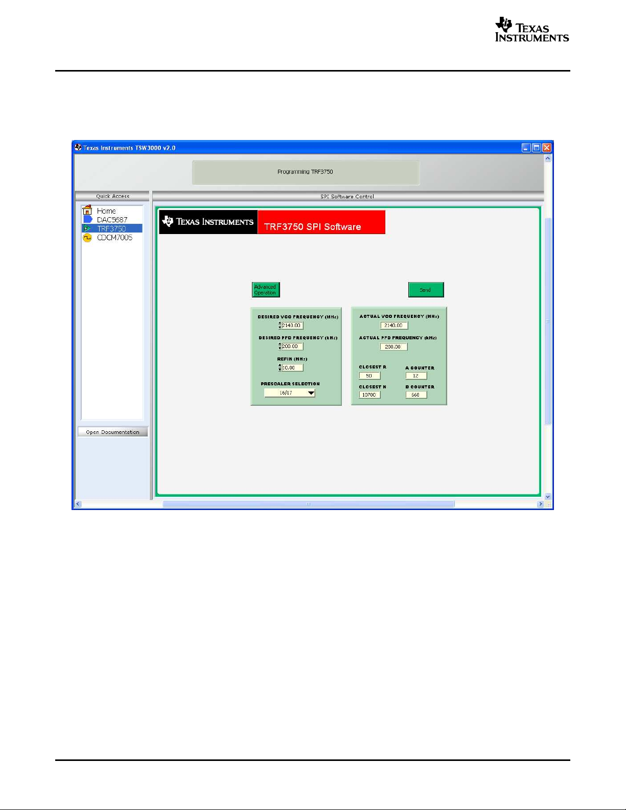
5.2 TRF3750 Software
The TRF3750 software is used to program the PLL chip to lock the VCO oto a desired frequency output.
The main menu of the program is shown in Figure 5 .
Figure 5. TRF3750 GUI - Main Menu
The options in the front panel allow the user to program the desired frequency of the VCO, the desired
frequency of the PFD, the reference frequency, and the prescaler selection. The software then displays
the actual VCO frequency, PFD frequency and the R, N, A, and B counter values to be programmed into
the TRF3750. Hitting the Send button writes these values to the TRF3750. In default mode on a default
board, only the desired VCO frequency (2100 MHz to 2200 MHz) needs to be changed. For other VCO
ranges, other parameters may need to be changed.
The Advanced Operation button will bring up another user interface as shown in Figure 6 .
12 SLWU013A – March 2004 – Revised September 2005
Page 13
www.ti.com
Software Operation
5.3 DAC5687 Software
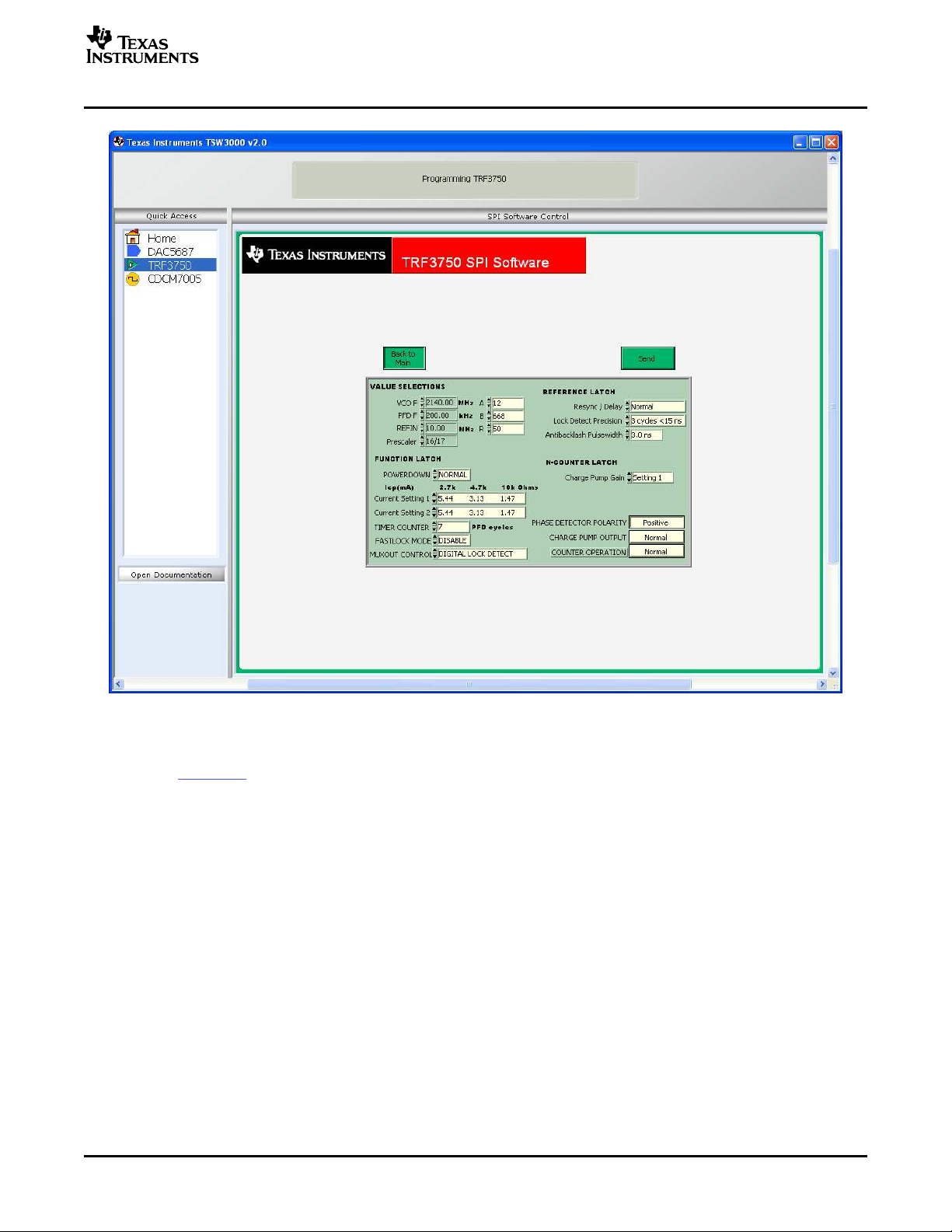
Figure 6. TRF3750 GUI - Advanced Menu
This menu allows control of more register settings. For details on these settings, see the TRF3750 data
sheet (SLWS146 ). The register of interest in this menu is the MUXOUT CONTROL which can be used to
determine the function of LED D4. This mode defaults to Digital PLL Lock Detect and causes the LED D4
to light up when the PLL successfully locks. Normally, these menu settings do not need to be changed.
By using the provided software, the user can write and read control register information to the DAC5687.
At first startup of this software, it is imperative to select the Pll Port Config button to bring up the parallel
port configuration settings. From the menu, select the TSW3000 setting. This configures the port to be
compatible with the TSW3000. Once the Demo Kit is powered on with the parallel port configured and
connected properly, then the GUI shown in Figure 7 is displayed with the default settings read from the
device. If there is a problem with the communication, such as the Demo Kit is not powered on or the
parallel port cable is not connected, an error message will be displayed instructing the user to correct the
problem. Once corrected, hit the Read All button to read the default settings of the device.
SLWU013A – March 2004 – Revised September 2005 13
Page 14

www.ti.com
Software Operation
For normal operation, the user needs only to select values and switches as desired. The values are
automatically sent to the device and read back to verify their configuration.
5.4 DAC5687 GUI Register Descriptions
5.4.1 Register Controls
• Load Regs– Loads register values from a saved file to the DAC5687 and updates the GUI.
• Save Regs– Saves current GUI registers settings to a text file for future use.
• Read All– Reads the current registers of the DAC5687. This is used to verify settings on the front
panel.
• Send All– Sends the current front panel registers to the device. This is generally only used when the
Demo Kit power has recycled or the device has been reset and the user wants to load the displayed
settings to the device.
5.4.2 Configuration Controls
• Full Bypass– When set, all filtering, QMC, and NCO functions are bypassed.
• FIR Bypass– Bypass all interpolation filters. QMC INCO functional. Limited to FDAC = 250 MHz
• FIFO Bypass– When set to bypass, the internal four sample FIFO is disabled. When cleared, the FIFO
is enabled.
• FIR A– A side first FIR filter in high-pass mode when set, low-pass mode when cleared.
Figure 7. DAC5687 GUI
14 SLWU013A – March 2004 – Revised September 2005
Page 15

www.ti.com
Software Operation
• FIR B– B side first FIR filter in high-pass mode when set, low-pass mode when cleared.
• Dual Clk– Only used when the PLL is disabled. When set, two differential clocks are used to input the
data to the chip; CLK1/CLK1C is used to latch the input data into the chip, and CLK2/CLK2C is used
as the DAC sample clock.
• Interleave– When set, interleaved input data mode is enabled; both A and B data streams are input at
the DA(15:0) input pins.
• Inverse Sinc– Enables inverse sinc filter.
• Half Rate Input– Enables half rate input mode. Input data for the DAC A data path is input to the chip
at half speed using both the DA(15:0) and DB(15:0) input pins.
• Sif– Sets sif_4-pin bit. A 4-pin serial interface mode is enabled when on, 3-pin mode when off. The
DAC5687 Demo Kit is configured for a 3-pin serial interface, so setting to a 4-bit serial interface makes
reading registers impossible with the GUI.
• Inv. PLL Lock– Only used when PLL is disabled and dual clock mode is disabled. When cleared, input
data is latched into the chip on rising edges of the PLLLOCK output pin. When set, input data is
latched into the chip on falling edges of the PLLLOCK output pin.
• PLL Freq– Sets PLL VCO center frequency to low or high center frequency.
• PLL Kv– Sets PLL VCO gain to either high or low gain.
• Qflag– Sets qflag bit. When set, the QFLAG input pin operates as a B sample indicator when
interleaved data is enabled. When cleared, the TXENABLE rising determines the A/B timing
relationship.
• 2's Comp– When set, input data is interpreted as 2's complement. When cleared, input data is
interpreted as offset binary.
• Rev A Bus– When cleared, DA input data MSB to LSB order is DA(15) = MSB and DA(0) = LSB.
When set, DA input data MSB to LSB order is reversed, DA(15) = LSB and DA(0) = MSB.
• Rev B Bus– When cleared, DB input data MSB to LSB order is DB(15) = MSB and DB(0) = LSB.
When set, DB input data MSB to LSB order is reversed, DB(15) = LSB and DB(0) = MSB.
• USB– When set, the data to DACB is inverted to generate upper side band output.
• Inv. Clk I(Q)– Inverts the DAC core sample clock when set, normal when cleared.
• Sync_Phstr– When set, the internal clock divider logic is initialized with a PHSTR pin low to high
transition.
• Sync_cm– When set, the coarse mixer is synchronized with a PHSTR low-to-high transition.
• Sync_NCO– When set, the NCO phase accumulator is cleared with a phstr low-to-high transition.
• Phstr Clk Div Select– Selects the clock used to latch the PHSTR input when restarting the internal
clock dividers. When set, the full rate CLK2 signal latches PHSTR and when cleared, the divided down
input clock signal latches PHSTR.
• DAC Serial Data– When set, both DAC A and DAC B input data is replaced with fixed data loaded into
the 16-bit serial interface DAC Static Data.
– Counter Mode– Controls the internal counter that can be used as the DAC data source: {off; all
16b; 7b LSBs; 5b MIDs; 5b MSBs}.
– DAC Static Data– When DAC Serial Data is set, both DAC A and DAC B input data is replaced
with fixed data loaded with this value. Range = 0 - 65535.
• Alt. PLLLOCK Output– Can be used to determine alternate outputs on the PLLLOCK pin when using
the internal PLL mode. The EXTLO pin must be open when using this mode.
• NCO– When set, enables NCO.
– NCO Gain– Sets NCO gain resulting in a 2x increase in NCO output amplitude. Except for Fs/2 and
Fs/4 mixing NCO frequencies, this selection can result in saturation for full-scale inputs. Consider
using QMC gain for lower gains.
• QMC– When set, enables the QMC.
– QMCA Gain– Sets QMC gain A to a range = 0 to 2047. See the data sheet for more information.
– QMC B Gain– Sets QMC gain B to a range = 0 to 2047. See the data sheet for more information.
– QMC Phase– Sets QMC phase to a range = -512 to 511. See the data sheet for more information.
Used to adjust for I/Q phase imbalance.
• Mode– Used to select the coarse mixer mode. See the DAC5687 data sheet for more information.
SLWU013A – March 2004 – Revised September 2005 15
Page 16

www.ti.com
Board Setup
• PLL Divider– Sets VCO divider to div by 1, 2, 4, or 8.
• Interpolation – Sets FIR Interpolation factor: {X2, X4, X4L, X8}. X4 uses lower power than 4xL, but
F
dac
• Phstr Init. Phase – Adjusts the initial phase of the fs/2 and fs/4 cmix block at PHSTR.
• Sync FIFO– Sync source selection mode for the FIFO. When a low to high transition is detected on
the selected sync source, the FIFO input and output pointers are initialized. See the DAC5687 data
sheet for source description.
5.4.3 DAC A(B) Gain
• DAC Coarse Gain– Sets coarse gain of DAC A(B) full-scale current. Range is 0 to 15. See the
DAC5687 data sheet for full-scale gain equation.
• DAC Fine Gain– Sets fine gain of DAC A(B) full scale current. Range is -128 to127. See the DAC5687
data sheet for full-scale gain equation. Used to adjust for I/Q amplitude imbalance.
• DAC DCOffset– Sets DAC A(B) dc-offset register. Range is -4096 to 4095. Used to adjust for carrier
suppression.
• Sleep– DAC A(B) sleeps when set, operational when cleared.
5.4.4 NCO
• NCO DDS– Sets NCO DDS registers. See the DAC5687 data sheet for formula.
• NCO Phase– Sets initial NCO phase registers. See the DAC5687 data sheet for more information.
• F
DAC
= 320 MHz max when NCO or QMC are used.
(MHz), NCO IF (MHz)– Used to calculate the required NCO DDS value.
5.4.5 Additional Control/Monitor Registers
• Version– Displays the version of the silicon. If a version of 0 is read then the communication is not
functioning and an error message will be displayed.
6 Board Setup
6.1 Jumper Settings
The TSW3000 Demo Kit has on-board jumpers that allow the user to selectively disengage devices as
desired. The unit is shipped with jumpers in place that activate all of the devices on board. Table 3
explains the functionality of the jumpers on the board.
JUMPER LABEL FUNCTION CONDITION DEFAULT
W1 PLL Lock 2-pin access port for monitoring PLL lock of the Open Installed
W2 PWD Power down for the TRF370x Powered Pin 1, 2
W6 LO Buffer Disengages power to LO buffer amp Powered Installed
W5 IOVDD Toggles 3.3 V or 1.8 V to IOVDD on the DAC5687 3.3 V Engaged Pin 1, 2
J15 pin 2 PLLVDD Toggles power to the DAC PLL Not Powered Pin 1, 2
J15 pin 5 SLEEP Power down for the DAC5687 Open Removed
J15 pin 8 EXTLO Toggles internal reference ground Grounded Pin 7, 8
J15 pin 11 TXENABLE Selects interleaved data Powered Pin 11, 12
J15 pin 14 TESTMODE DO NOT POPULATE! Open Removed
J15 pin 17 QFLAG Used to flag the DAC5687 channel B data in Open Removed
J15 pin 20 CDC_PD Power down of the CDCM7005 Open Removed
J15 pin 23 REF_SEL Selecets reference for CDCM7005 Open Removed
Table 3. Jumper List
DAC5687
interleave mode
16 SLWU013A – March 2004 – Revised September 2005
Page 17

www.ti.com
6.2 Input/Output Connectors
The input and output connections are shown in Table 4 .
Demo Kit Test Configuration
Table 3. Jumper List (continued)
JUMPER LABEL FUNCTION CONDITION DEFAULT
J15 pin 27 PLL_PWD Power down the TRF3750 Powered Pin 26, 27
J15 pin 29 RESET Resets the DAC5687 when low Open Removed
Table 4. Input/Output Connections
REFERENCE DESIGNATOR CONNECTOR TYPE DESCRIPTION
J13 34-pin header I channel data input
J14 34-pin header Q channel data input
J9 SMA RF output
J10 SMA Optional LO input
J8 SMA Optional external reference
J2 SMA Output clock 1 from CDCM7005
J3 SMA Output clock 2 from CDCM7005
J5 SMA Optional I out A from DAC5687
J19 SMA Optional Q out B from DAC5687
J6 SMA Input for external VCXO for CDCM7005
J7 SMA PLL lock status on DAC5687
J4 SMA Phase synchronization on DAC5687
RF shield covers should be in place over the synthesizer section and the RF modulator section. These
shields provide isolation of the RF sections on the board.
6.3 Parallel Port
The TSW3000 Demo Kit contains a 25-pin parallel port connector (J1) to interface to a standard computer
parallel port. Programming of the CDCM7005, DAC5687, and TRF3750 are accomplished through this
port.
6.4 DC Power Requirements
The Demo Kit requires a single dc-voltage supply that is nominally 6 V. From that supply, the 5 V, 3.3 V,
and 1.8 V required for the devices on the board are generated internally through linear voltage regulators.
It is possible to use a higher input voltage; however, care should be taken not to over dissipate the
on-board voltage regulators.
7 Demo Kit Test Configuration
SLWU013A – March 2004 – Revised September 2005 17
Page 18

www.ti.com
TSW3000
EVM DUT
J7
Clock
Power
Supply
GND
+6 V
16
25
J9
Pattern
Generator
16
J17 J11
PC Controller
J14
J13
J1
Spectrum
Analyzer
Demo Kit Test Configuration
7.1 Test Setup Block Diagram
The test set up for general testing of the TSW3000 Demo Kit is shown in Figure 8 .
Figure 8. Test System Block Diagram
7.2 Test Equipment
7.3 Calibration
7.4 Test Specifications
The following is a list of the test equipment required for testing the TSW3000 Demo Kit. Equivalent models
may be used for certain applications, but may produce different results due to limitations within the
instrument.
• Dual Power Supply: Any with current readout capability
• Spectrum Analyzer: Rhode & Schwartz FSU, Agilent PSA, or equivalent
This particular piece can measure >70-dBc ACPR with the noise cancellation option active. This
amount of dynamic range is required to accurately measure the ACPR of the Demo Kit. Another
spectrum analyzer can be substituted if it achieves as good or better dynamic range.
• Pattern Generator: Agilent 16702B
• Oscilloscope: Tektronix 650 or equivalent
Used to probe clock output signals and for debugging.
• Digital Voltmeter: Agilent 34401A or equivalent
In order to record proper output power the insertion loss of the output cable must calibrated. Measure the
insertion loss of the cable from J9 to the spectrum analyzer; set the analyzer's reference level offset to
that value.
The test specifications are outlined in Table 5 .
Table 5. Demo Kit Specifications
CURRENT
+6 V 1.5 A
CW TESTS
Carrier suppression 30 dBc
MIN MAX UNITS
18 SLWU013A – March 2004 – Revised September 2005
Page 19

www.ti.com
8 Basic Test Procedure
Basic Test Procedure
Table 5. Demo Kit Specifications (continued)
MIN MAX UNITS
Sideband rejection 25 dBc
Spurious Output
2nd harmonic 45 dBc
Aliased LSB (pos) 40 dBc
Output clock 40 dBc
Aliased USB 15 dBc
Aliased USB (neg) 8 dBc
WCDMA ACPR
Channel power -14 dBm
ACPR -Low 70 dBc
ACPR -High 70 dBc
This section outlines the basic test procedure to get the Demo Kit operational. Disconnect the cables at
J13 and J14 that connect to the pattern generator. Connect the power supply cable and the RF output to
the spectrum analyzer.
8.1 Initial Inspection
Inspect the board to determine which devices were used.
• Note the VCXO frequency (U10) that is on the board
• Note the VCO frequency band (Y3) that is on the board
8.2 Engage Power Supplies
Engage 6-V power supply
• Verify the current reading is between 0.8 A to 1.3 A when configured with the DAC5687
8.3 Program the CDCM7005
Use the Default Settings on the CDCM7005 GUI (See Section 5.1 ). This generates a 491.52-MHz clock.
• Set the OUT_MUX_0, 2, 3, 4 to tristate. Only OUT_MUX_1 is used for clocking the DAC5687
• Hit the GUI Send button
• Verify that LEDs D1, D2, and D3 are illuminated
8.4 Program the TRF3750
Use the Default Settings in the TRF3750 GUI (See Section 5.2 ). This places a carrier at 2.14 GHz
• Hit the GUI send button.
• Verify the LED D4 is illuminated. This indicates lock of the VCXO and TCXO reference.
• Monitor RF output from the spectrum analyzer
• Verify a single frequency tone at the default 2.14 GHz.
Table 6. Frequency Designations
VCO BAND UMTS GSM900 PCS DCS1800
Midband (MHz) 2140 950 1960 1850
Low (MHz) 2110 935 1930 1805
SLWU013A – March 2004 – Revised September 2005 19
Page 20

www.ti.com
Basic Test Procedure
8.5 DAC5687 Program
Table 6. Frequency Designations (continued)
VCO BAND UMTS GSM900 PCS DCS1800
High (MHz) 2170 960 1990 1880
• Disable the PLL by removing the jumper at J15, pins 2 and 3, if not already removed.
• Verify DACA and DACB Coarse Gain is set to 15
• Set Mode to 0000 (No Coarse Mixing)
• Ensure DAC Offsets and DAC fine gain for both A and B are set to 0
• Set the spectrum analyzer as follows:
– Center Freq: 2.14 GHz
– RBW: 30 kHz, VBW: 300 kHz
– Span: 491.52 MHz
– Attn: 5 dB
– Ref Level: 10 dBm
20 SLWU013A – March 2004 – Revised September 2005
Page 21

www.ti.com
Basic Test Procedure
8.6 Carrier Suppression
The carrier suppression can be tuned for better performance by adjusting the dc-offset controls on the
DAC5687. The default DAC GUI is shown below with the NCO mixer turned on to output a 61.44-MHz
tone. The output spectrum is illustrated in Figure 10 .
Figure 9. Default DAC GUI With f
SLWU013A – March 2004 – Revised September 2005 21
/8 Tone From NCO
DAC
Page 22

www.ti.com
Basic Test Procedure
8.7 Sideband Rejection
Figure 10. Single Sideband Spectrum Output Before DAC Offset and QMC Adjustments
An iterative process is used to achieve the best performance.
• Place a normal marker at the peak upper sideband, place a delta marker at the carrier signal, and note
the initial delta value.
• Set initial DACA offset to 1000 and DACB offset to -1000
• Change DACA offset by 1000 steps and monitor the output performance change.
• If performance gets better, then repeat the process with an additional 1000 steps. If the performance
gets worse or doesn't change, then change the offset in the other direction by 1000 steps.
• Once the performance remains basically unchanged, repeat the process on DACB offset with 1000
step changes.
• Once optimized, go back to the A side and repeat the tuning process with a step size of 100.
• Continue tuning. After each complete cycle, reduce the step size down (i.e., to 10, then to 1 if desired).
• A performance greater that 65 dBc should be achievable.
Sideband rejection is determined by the two quadrature signals to the modulator being exactly 180
degrees out of phase and exactly the same amplitude. Amplitude and phase imbalance between the two
paths yield an unwanted lower sideband. The amplitude variation between the two paths can be
compensated for by adjusting the DAC fine gain controls or by adjusting the QMC gain controls if the
device is operating with the QMC on. The phase can be compensated by using the QMC phase
adjustment. Note this is only possible when the coarse mixer is not used in the f
mixing in the f
f
/2 mode there are no cross terms (terms are 0) and the relative phase information is maintained
DAC
/4 mode causes the relative phase information between I and Q paths to be mixed. In the
DAC
/4 mode. Coarse
DAC
between I and Q paths.
22 SLWU013A – March 2004 – Revised September 2005
Page 23
www.ti.com
Basic Test Procedure
• Place marker delta on the lower sideband
• Turn on the QMC. Set the Gain of the QMC to 1024 for gain of 0 dB for I and Q paths. Other initial
settings may be needed depending on the state of the NCO gain and signal amplitude.
• Change the phase of the QMC by small increments until the sideband is minimized.
• Change the QMC A or B gains in increments of 1 until the sideband is minimized.
• The overall performance should be greater than 60 dBc from the other sideband with amplitude and
phase corrections.
• Re-optimized the dc-offset values as required to maintain carrier suppression performance as
specified.
Figure 11. DAC GUI With Typical Settings To Minimize LO and Sideband
Sideband and LO are reduced into the noise floor. Clock related spurs can be filtered out using an RF
filter.
SLWU013A – March 2004 – Revised September 2005 23
Page 24

www.ti.com
Optional Configurations
9 Optional Configurations
9.1 External LO
To configure the board for external LO implement the following modifications
• Remove R225
• Place R2: 0- Ω resistor, this connects the external LO on J10 to the TRF3702 modulator
• Remove W6 (disengages power to RF amplifier)
• Disable the TRF3750 PLL CE by setting J15-25, 26. This puts GND on CE of the TRF3750 and
disables the PLL.
9.2 External Reference
To configure the board for an external reference implement the following modifications.
• Remove R144, this disconnects the on board 10-MHz reference
• Place R201: 0- Ω resistor, external reference can be hooked up to J8
9.3 Monitor DAC Output
Figure 12. Sideband and LO
24 SLWU013A – March 2004 – Revised September 2005
Page 25

www.ti.com
9.3.1 Single Ended
To configure the board to monitor the DAC output by utilizing the transformers on board to achieve a
single-ended output, implement the following modifications.
• Remove R187, R188, R191, R190, R208, R209, R210, R211
• Place R200, R224, R222, R223: 0- Ω resistors
• Place R179, R183, R212, R213: 100- Ω resistor. This configures the DAC output as in the DAC5687
data sheet for 4:1 impedance transformer.
Monitor outputs at J5 and J19.
10 Filter Specifications
10.1 Baseband Filter
The TSW3000 Demo Kit layout provides the opportunity to place components to realize up to a 7thorder
LC filter. The Demo Kit is by default populated with a 500-MHz LC low-pass filter to help eliminate DAC
images and also out of band clock spurs which may mix into RF frequencies.
10.1.1 RF Filter/Output Match
The TSW3000 Demo Kit layout also provides the opportunity to place a small 3
output of the modulator for either filtering or impedance matching purposes. This filter has been disabled
by removing the shunt capacitive elements and replacing the series inductor element with a 0- Ω resistor.
Filter Specifications
rd
order LC filter on the
11 Layers and Schematics
This chapter contains the layers and schematics for the TSW3000 Demo Kit.
SLWU013A – March 2004 – Revised September 2005 25
Page 26
www.ti.com
Layers and Schematics
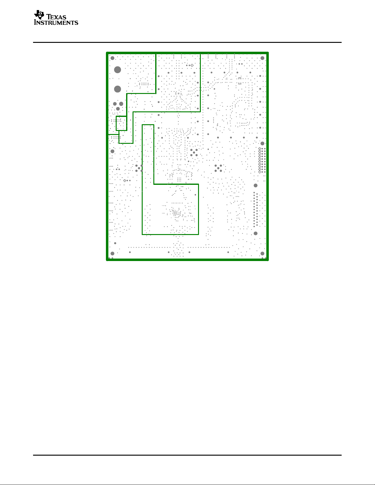
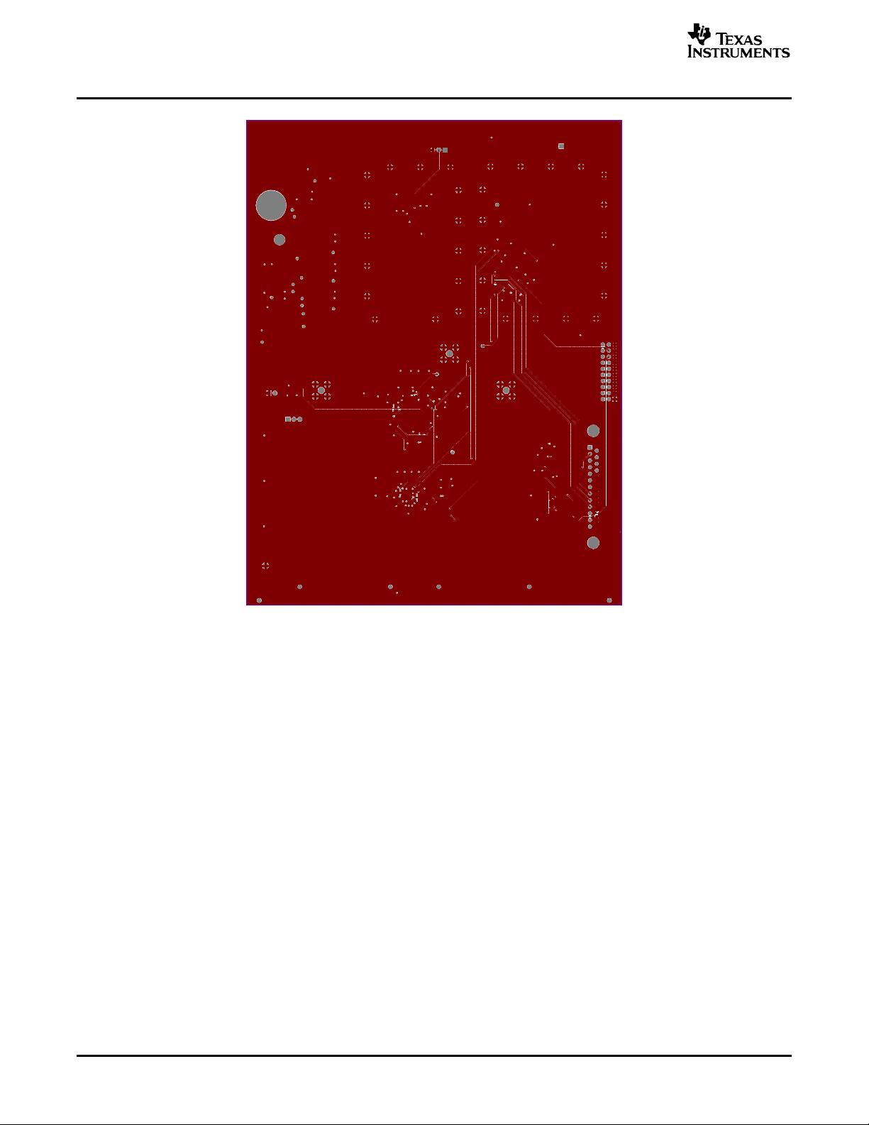
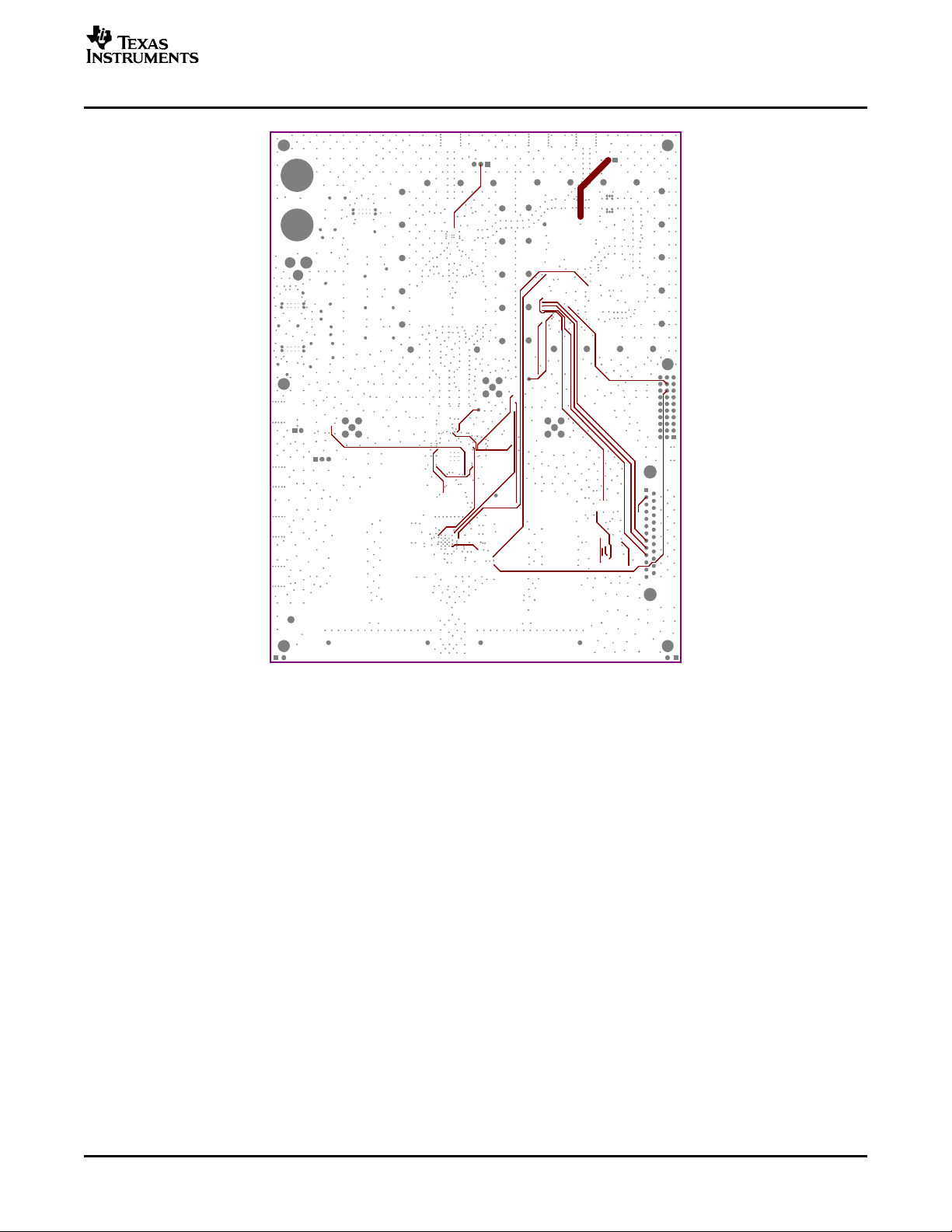
11.1 Layers
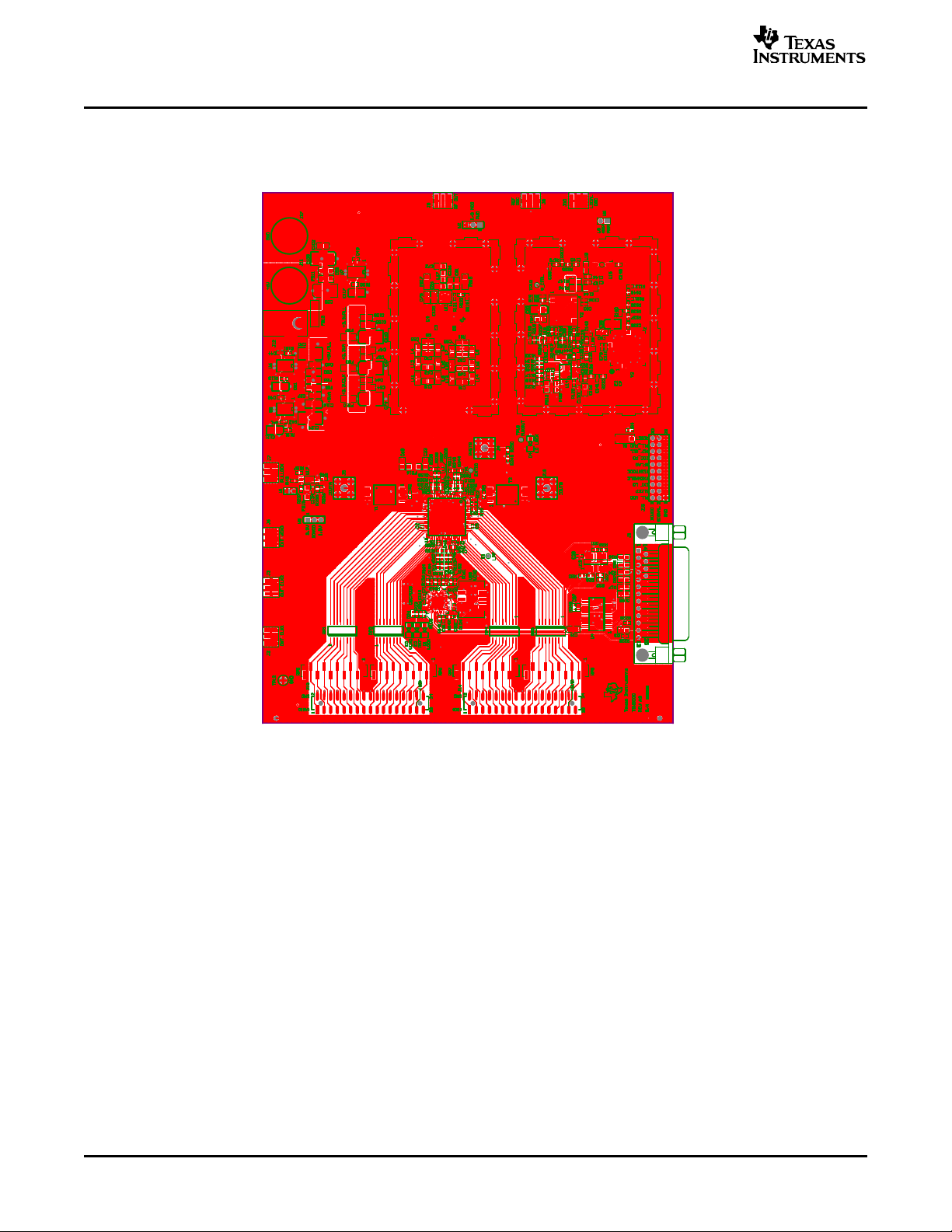
The Demo Kit is constructed on a 6-layer, 6.2 inch x 8 inch, 0.062-inch thick PCB using FR-4 material.
See Figure 13 through Figure 22 show the PCB layout for the Demo Kit.
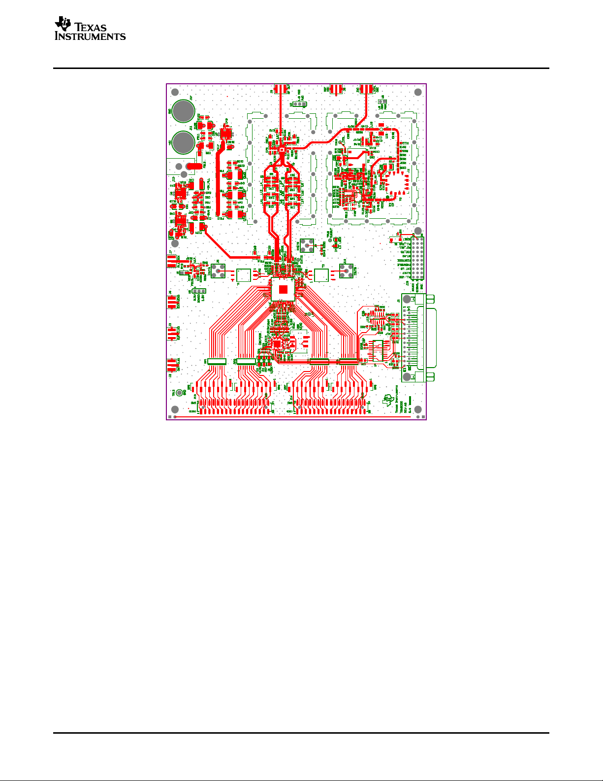
Figure 13. Top Layer
26 SLWU013A – March 2004 – Revised September 2005
Page 27
www.ti.com
Layers and Schematics
Figure 14. Top Layer (NH)
SLWU013A – March 2004 – Revised September 2005 27
Page 28

www.ti.com
Layers and Schematics
Figure 15. Layer 2
28 SLWU013A – March 2004 – Revised September 2005
Page 29
www.ti.com
Layers and Schematics
Figure 16. Layer 3
SLWU013A – March 2004 – Revised September 2005 29
Page 30
www.ti.com
Layers and Schematics
Figure 17. Layer 4
30 SLWU013A – March 2004 – Revised September 2005
Page 31
www.ti.com
Layers and Schematics
Figure 18. Layer 4 (NH)
SLWU013A – March 2004 – Revised September 2005 31
Page 32

www.ti.com
Layers and Schematics
Figure 19. Layer 5
32 SLWU013A – March 2004 – Revised September 2005
Page 33

www.ti.com
Layers and Schematics
Figure 20. Bottom Layer
SLWU013A – March 2004 – Revised September 2005 33
Page 34

www.ti.com
Layers and Schematics
Figure 21. Bottom Silkscreen
34 SLWU013A – March 2004 – Revised September 2005
Page 35

www.ti.com
Layers and Schematics
Figure 22. Drill Drawing
11.2 Schematics
The following figures show the schematic for the TSW3000 Demo Kit.
SLWU013A – March 2004 – Revised September 2005 35
Page 36

+3.3VA
C15
.1uF
C29
.1uF
C84
.1uF
C85
.1uF
C86
.1uF
C24
+
10uF, 10V
(SH 2)
EXT_LO
EXT_LO
TP1
54321
+1.8VD
+3.3VA
R4
1K
S1
R1
1K
6
D
+1.8VD
C38
+
10uF, 10V
(SH 5)
SDEN1
(SH 5)
(SH 5)
C
B
A
(SH 2)
TXENABLE
IOVDD
(SH 2)
SCLK
SDIO
C39
+
10uF, 10V
DA(0..15)
C1
.1uF
C37
+
10uF, 10V
C2
.1uF
SDEN1
SCLK
SDIO
TXENABLE
R40
49.9
NOTES:
1. DO NOT INSTALL
2. CHANGE TO 0 OHM FOR 50 OHM LOAD
1 2 3 4 56
C4
.1uF
DA15
DA14
DA13
DA12
DA11
DA10
DA9
DA8
DA7
DA6
DA5
DA4
DA3
DA2
DA1
DA0
C5
.1uF
.1uF
C17
C6
.1uF
+1.8VD
C7
.1uF
26
DVDD
27
DGND
28
SDENB
29
SCLK
30
SDIO
31
SDO
32
DVDD
33
TXENABLE
34
DA15
35
DA14
36
DA13
37
DVDD
38
DGND
39
DA12
40
DA11
41
DA10
42
DA9
43
DA8
44
DVDD
45
DGND
46
IOVDD
47
IOGND
48
DA7
49
DA6
50
DA5
R255
10
+3.3VCLK
C41
10uF, 10V
C16
.1uF
+3.3VA +3.3VA
8
10
13
14
16
22
21
AGND
.1uF
C13
.1uF
19
20
AGND
IOUTA2
IOUTA1
18
AVDD
17
AGND
15
AVDD
AVDD
EXTLO
U1
DAC5687
KIT A
12
BIASJ
AGND
11
EXTIO
C14
.1uF
9
AVDD
AGND
7
AVDD
AGND
E1
C40
+
10uF, 10V
5
6
IOUTB2
70
23
24
25
AVDD
AVDD
AGND
DA451DA352DA253DA154DA055DVDD56DGND57CLKGND58CLK159CLK1C60CLKVDD61CLK262CLK2C63CLKGND64PLLGND65LPF66PLLVDD67DVDD68DGND69PLLLOCK
C3
+
2
3
1
4
AVDD
AVDD
AGND
AGND
IOUTB1
QFLAG
TESTMODE
SLEEP
/RESETB
PHSTR
IOVDD
IOGND
DB071DB172DB273DB374DB4
75
CLK2C
CLK2
CLK1C
CLK1
C8
.1uF
DVDD
DGND
DGND
DB15
DB14
DB13
DVDD
DGND
DB12
DB11
DB10
DB9
DB8
DVDD
DGND
DB7
DB6
DB5
93.1
R25
R45
100
100
99
98
97
96
95
94
93
92
91
90
89
88
87
86
85
84
83
82
81
80
79
78
77
76
C33
.01uF
R150
100
330pF
C46
C56
C34
.01uF
.033uF
C52
C62
DB4
DB3
DB2
DB1
DB0
.01uF
.01uF
SW-PB
RESET
C9
.1uF
QFLAG
TESTMODE
SLEEP
DB15
DB14
DB13
DB12
DB11
DB10
DB9
DB8
DB7
DB6
DB5
PLL_VDD
CLK2CB
CLK2B
CLK1CB
CLK1B
RESET
C10
.1uF
(Sh 2, 4)
C11
.1uF
R12
49.9
(Note 1)
IOVDD
DB[0..15]
PLL_VDD
CLK2CB
CLK2B
CLK1CB
CLK1B
C18
.1uF
(SH 2)
(SH 5)
(SH 5)
(SH 5)
(SH 5)
C12
.1uF
QFLAG
TESTMODE
SLEEP
R39
49.9
DB(0..15)
(SH 2)
R13
+3.3VA
1
2
3
(SH 2)
49.9
W5
(1-2)
IOUTA1
IOUTA2
IOUTB2
IOUTB1
(SH 2)
R249
0
PHSTR
+1.8VD
(SH 2)
(Note 1)
R250
0
PHSTR
(SH 2)
+3.3VA
1
2
+3.3VA
FB15
FERRITE
3 4
5
R235
110
(Note 1)
(Note 1)
J4
MCX
R236
221
C134
.1uF
C153
+
10uF, 10V
1
CLKIN
6
VDD/3.3V
2
OE
4
GND
IOUTA1
IOUTA2
IOUTB2
IOUTB1
U17
CDCV304
(SH 3)
(SH 3)
(SH 3)
(SH 3)
1Y0
1Y1
1Y2
1Y3
Engineer:
Drawn By:
FILE:
3
5
7
8
R46
R43
R237
22.1
R. HOPPENSTEIN
Y. DEWONCK
49.9
49.9
W1
R197
22.1
(Note 2)
1
2
ti
12500 TI Boulevard. Dallas, Texas 75243
Title:
SIZE: DATE: REV:
TSW3000
14-Jul-2005
3 4
J7
SMA
5
A3
17
SHEET: OF:
D
C
B
A
Page 37

54321
6
DATA PORT 1
J13
12
34
56
78
910
D
C
1112
1314
1516
1718
1920
2122
2324
2526
2728
2930
3132
3334
34PIN_IDC
A15
A14
A13
A12
A11
A10
A9
A8
A7
A6
A5
A4
A3
A2
A1
A0
PHSTR
PHSTR
(SH 1)
RP5
51
(Note 1)
2345678910
RP6
51
(Note 1)
1
2345678910
1
DATA PORT 2
J14
1112
1314
1516
1718
B
1920
2122
2324
2526
2728
2930
3132
3334
34PIN_IDC
B0
12
B1
34
B2
56
B3
78
B4
910
B5
B6
B7
B8
B9
B10
B11
B12
B13
B14
B15
RP1
22
1 16
2 15
3 14
4 13
5
6
7
8
1 16
2 15
3 14
4 13
5
6
7
8
RP2
22
RP4
22
9
10
11
12
9
10
11
12
RP3
22
DA15
DA14
DA13
DA12
12
11
10
9
12
11
10
9
8
7
6
5
413
314
215
116
8
7
6
5
413
314
215
116
DA11
DA10
DA9
DA8
DA7
DA6
DA5
DA4
DA3
DA2
DA1
DA0
DB0
DB1
DB2
DB3
DB4
DB5
DB6
DB7
DB8
DB9
DB10
DB11
DB12
DB13
DB14
DB15
DA(0..15)
DB(0..15)
(SH 1)
(SH 1)
+3.3VA
J15
1
3
4
6
7
9
101112
131415
161718
192021
222324
252627
282930
2
5
8
PLL_VDD
SLEEP
EXT_LO
TXENABLE
TESTMODE
QFLAG
CDC_PD
REF_SEL
PLL_PWD
RESET
3 ROW 30 PIN CONNECTOR
PLL_VDD
SLEEP
EXT_LO
TXENABLE
TESTMODE
QFLAG
CDC_PD
REF_SEL
PLL_PWD
RESET
D
C
(SH 1)
(SH 1)
(SH 1)
(SH 1)
(SH 1)
(SH 1)
(SH 4)
(Sh 4)
(Sh 7)
(SH 1, 4)
B
A
NOTES:
1. DO NOT INSTALL
2345678910
RP7
51
(Note 1)
1 2 3 4 56
1
RP8
51
(Note 1)
2345678910
A
1
Title:
Engineer:
Drawn By:
FILE:
R. HOPPENSTEIN
Y. DEWONCK
DOCUMENTCONTROL #
DATE:
ti
12500 TI Boulevard. Dallas, Texas 75243
TSW3000
14-Jul-2005
SIZE:
SHEET: OF:
A3
REV:
7
2
Page 38
54321
6
R189
15
+3.3VA
0
+3.3VA
VCM
VCM
R238
49.9
R243
49.9
R239
49.9
T1
1
2
3
T4-1T-KK81
R244
49.9
C23
.1uF
6
4
C31
2.2pF
C19
2.2pF
FB16
L13
18 nH
L14
18 nH
L9
18nH
L11
18 nH
1
2
+5VA
IOUTA
3 4
C68
2.2pF
5
C65
6.8pF
C63
6.8pF
J5
SMA
L10
2.7 nH
L12
2.7 nH
L15
2.7 nH
L16
2.7 nH
C32
1pF
C30
1pF
L7
0 nH
L8
0 nH
L2
0nH
L4
0nH
E3
IREF
C93
E4
E5
E6
47pF
(Note 1)
C95
47pF
(Note 1)
R11
R8
2K
5
9
GND
VCC
PWD
GND
C125
1pF
R122
18.2
R121
274
6
7
8
C26
.1uF
FB17
C75
.1uF
ISIG
3
4
11
GND
LO
RFOUT
VCC
10
C20
.1uF
GND1GND2GND
16
QREF
15
IREF
14
IVIN
QVIN
13
QREF
2K
QSIG
U11
TRF3702
GND
12
R119
274
C66
(Note 2)
(Note 1)
C126
1pF
LOCAL_OSC
L17
(Note 2)
+5VA
C81
.1uF
0
(Note 2)
(Note 1)
LOCAL_OSC
FB18
TP12
+5VA
2
1
3
C72
+5VA
(SH 7)
W2
(1-2)
1
J9
SMA
3 4
5
2
REFOUT
D
C
B
+3.3VA
R179
100
(Note 1) (Note 1)
(Sh 1)
(Sh 1)
(Sh 1)
(Sh 1)
IOUTA1
IOUTA2
IOUTB1
IOUTB2
D
C
B
IOUTA1
IOUTA2
+3.3VA
IOUTB1
IOUTB2
R183
100
R208
221
R212
100
(Note 1) (Note 1)
R209
221
(Note 1)
R200
0
(Note 1)
R224
0
R213
100
R210
221
R187
R188 15
R2
100
(Note 1)
R191 15
R190 15
R211
221
A
NOTES:
1. DO NOT INSTALL
R193
(Note 1)
R222
0
(Note 1)
R223
0
R5
100
(Note 1)
0
T2
3
2
1
T4-1T-KK81
4
6
1
IOUTB
2
3 4
5
J19
SMA
A
ti
12500 TI Boulevard. Dallas, Texas 75243
Title:
Engineer:
R. HOPPENSTEIN
Drawn By:
Y. DEWONCK
FILE:
1 2 3 4 56
DOCUMENTCONTROL #
DATE:
14-Jul-2005
TSW3000
SIZE:
REV:
37
SHEET: OF:
A3
Page 39

54321
6
D
(Sh 7)
C
B
C99
10uF, 10V
A
NOTES:
1. DO NOT INSTALL
REF_OSC
R124
(Note 1)
V_CTRL
+3.3VCLK
+
0
REF_OSC
CDC_PD
U10
VCXO1
3
GND
EN2OUT_B
1
V_CTRL
TOYOCOM
2115-491.52MHZ
C110
560pF
C89
.1uF
R7
1K
(Note 1)
OUT
VCC
J6
SMA END
5
4
5
6
1
3 4
2
C88 1000pF
R6
0
R9
0
+3.3VCLK
R151
10K
R128
130
(Sh 2)
(Sh 1, 2)
R126
82.5
(Sh 2)
CDC_PD
RESET
R14
0
R149
10K
(Sh 5)
CTRL_LE
(Sh 5)
CTRL_DATA
(Sh 5)
CTRL_CLK
+3.3VCLK
C36
.1uF
+3.3VCLK
R129
130
R10
0
(Note 1) (Note 1)
C45
.1uF
R127
82.5
REF_SEL
REF_IN
CTRL_LE
CTRL_DATA
CTRL_CLK
VBB
REF_SEL
CDC_REF
CDC_PD
RESET
VCXO_INB
VCXO_IN
OUT CLK2
OUT CLK1
J2
SMA END
3 4
5
2
J3
SMA END
3 4
5
2
35
REF_SEL
36
PRI_REF
29
CTRL_LE
26
CTRL_DATA
28
CTRL_CLK
37
SEC_REF
1
/PD
33
VCC_CP
14
/RESET/HOLD
42
/VCXO_IN
43
VCXO_IN
1
1
R16
22.1
R18
22.1
CDCM7005
+3.3VCLK
R19
100
+3.3VCLK
R20
100
U12A
VBB
STATUS_REF
STATUS_VCXO
PLL_LOCK
CP_OUT
YOA
YOB
Y1A
Y1B
Y2A
Y2B
Y3A
Y3B
Y4A
Y4B
C87
.1uF
R21
100
C90
.1uF
R22
100
40
23
22
25
31
46
47
3
4
7
8
11
12
16
17
Y4
R33
150
(Note 1)
Y3
R38
150
(Note 1)
VBB
R221
150
R15
150
+3.3VCLK
CDC_LCK
R152
R153
R154
R156
130
130
130
130
R161
R162
R163
R164
82.5
82.5
82.5
82.5
U12B
CDCM7005
24
GND
VCC
VCC
VCC
VCC
VCC
VCC
VCC
VCC
VCC
VCC
VCC
VCC
VCC
VCC
VCC
AVCC
AVCC
AVCC
AVCC
AVCC
2
5
6
9
10
13
15
18
19
20
21
41
44
45
48
27
30
32
38
39
R109
0
(Note 1)
CP_OUT
CDC_REF
C101
+
10uF
C22
+
10uF
CDC_REF
C49
.1uF
FB14
FERRITE
R23
R24
R26
R172
R110
R114
R171
C114
.1uF
CDC_LCK
750
750
750
(SH 7)
0
0
0
0
C58
.1uF
C69
.1uF
C73
.1uF
CLK2B
CLK2CB
CLK1B
CLK1CB
(Sh 5)
C71
.01uF
C104
.1uF
D2
D1
CLK2B
CLK2CB
CLK1B
CLK1CB
C100
.1uF
C122
.01uF
CLOCK DISTRIBUTION
D3
R142
162
C96
22uF
C91
1uF
+3.3VCLK
C119
.001uF
C120
.1uF
AVCC
C112
.1uF
C131
.001uF
(Sh 1)
(Sh 1)
(Sh 1)
(Sh 1)
C113
.1uF
R141
4.75K
+
C115
.1uF
D
V_CTRL
C92
.47uF
C
B
A
ti
12500 TI Boulevard. Dallas, Texas 75243
Title:
Engineer:
R. HOPPENSTEIN
Drawn By:
Y. DEWONCK
FILE:
1 2 3 4 56
DOCUMENTCONTROL #
DATE:
14-Jul-2005
TSW3000
SIZE:
REV:
47
SHEET: OF:
A3
Page 40

+3.3VA
D
J1
DB25F-RA
1
DATA
CLK
SDEN1
SDEN2
SDIO
C
B
2
3
4
5
6
7
8
9
10
11
12
13
14
15
16
17
18
19
20
21
22
23
24
25
VCOMM_CS
CDC_LCK
PLL_DATA
PLL_CLK
PLL_LCK
CDC_LCK
R228
0
(Note 1)
VCOMM_CS
PLL_DATA
PLL_CLK
PLL_LCK
(Sh 4)
(Sh 4)
(SH 7)
(SH 7)
(SH 7)
VCOMM_CLK
VCOMM_DATA
R34
R35
R36
R37
R17
R155
R247
VCOMM_CLK
VCOMM_DATA
10K
10K
10K
10K
10K
10K
0
(Sh 4)
(Sh 4)
R3
R229
0
(Note 1)
1
2
4
6
8
11
13
15
17
10
10
2
5
9
12
1
4
7
SN74HC241DW
OE1
1A1
1A2
1A3
1A4
2A1
2A2
2A3
2A4
GND
SN74LV125AD
1A
2A
3A
4A
1OE
2OE
GND
U4
20
VCC
19
OE2
18
1Y1
16
1Y2
14
1Y3
12
1Y4
9
2Y1
7
2Y2
5
2Y3
3
2Y4
U13
14
VCC
3
1Y
6
2Y
8
3Y
11
4Y
13
4OE
10
3OE
C97
10pF
+3.3VA
C21
.1uF
SDIO
SCLK
SDEN1
R248
10K
C28
.1uF
R28
R27
R29
+3.3VA
+3.3VA +3.3VA
100
100
+3.3VA
100
SDIO
SCLK
SDEN1
R30
100K
R31
100K
C61
10pF
C127
10pF
(Sh 1)
(Sh 1)
(Sh 1)
R32
100K
C128
10pF
CTRL_CLK
CTRL_DATA
CTRL_CLK
CTRL_DATA
CTRL_LE
(Sh 4)
(Sh 4)
(Sh 4)
D
C
B
PLL_LE
A
PLL_LE
(SH 7)
A
ti
12500 TI Boulevard. Dallas, Texas 75243
NOTES:
1. DO NOT INSTALL
1 2 3 4 56
Engineer:
Drawn By:
FILE:
R. HOPPENSTEIN
Y. DEWONCK
Title:
DOCUMENTCONTROL #
DATE:
14-Jul-2005
TSW3000
SIZE:
REV:
57
SHEET: OF:
A3
Page 41

6V
J11
C57
.01uF
+3.3VA
+
C67
47uF
C54
1uF
+3.3VCLK
C64
.01uF
+
47uF
C74
J12
1
2
3
3POS-POWER-JACK
RED
J17
BLACK
FB13
AVDD
D
+6V
C43
.1uF
1
GND/HSINK
2
GND/HSINK
3
GND
4
NC
5
EN_
6
IN
7
IN
8
NC
9
GND/HSINK
10
GND/HSINK
GND/HSINK
GND/HSINK
U7
TPS76733QPWP
GND/HSINK
GND/HSINK
NC
NC
RESET_
FB/NC
OUT
OUT
20
19
18
17
16
15
14
13
12
11
R130
100K
C117
+
10uF, 10V
FB3
C47
1uF
FB10
6V
+
C25
47uF
FB11
C53
1uF
C102
.01uF
+6V
+
47uF
C105
D
C
C109
.01uF
+6V
R181
0
+
+3.3VPLL
(Note 1)
C116
10uF, 10V
+
47uF
C160
C50
1uF
+5VA
C27
.1uF
C60
.01uF
+5V_PLL
+
47uF
+6V
C48
.1uF
C70
FB7
C159
1uF
B
+6V
C44
.1uF
1
GND/HSINK
2
GND/HSINK
3
GND
4
NC
5
EN_
6
IN
7
IN
8
NC
9
GND/HSINK
10
GND/HSINK
GND/HSINK
GND/HSINK
U6
TPS76750QPWP
GND/HSINK
GND/HSINK
NC
NC
RESET_
FB/NC
OUT
OUT
20
19
18
17
16
15
14
13
12
11
R113
100K
C51
+
10uF, 10V
FB6
FB1
+
47uF
C124
1
GND/HSINK
2
GND/HSINK
3
GND
4
NC
5
EN_
6
IN
7
IN
8
NC
9
GND/HSINK
10
GND/HSINK
GND/HSINK
GND/HSINK
U8
TPS76701QPWP
GND/HSINK
GND/HSINK
NC
NC
RESET_
FB/NC
OUT
OUT
20
19
18
R131
100K
10uF, 10V
C121
+1.8VD
+
R41
15.8K
R42
30.1K
17
16
15
14
13
12
11
C
B
A
A
ti
12500 TI Boulevard. Dallas, Texas 75243
NOTES:
1. DO NOT INSTALL
1 2 3 4 56
Engineer:
Drawn By:
FILE:
R. HOPPENSTEIN
Y. DEWONCK
Title:
DOCUMENTCONTROL #
DATE:
14-Jul-2005
TSW3000
SIZE:
REV:
67
SHEET: OF:
A3
Page 42
+3.3VA
D
C
B
A
(SH 5)
(SH 5)
(SH 5)
NOTES:
(SH 4)
PLL_CLK
PLL_DATA
PLL_LE
CDC_REF
PLL_CLK
PLL_DATA
PLL_LE
REF IN
FB8
PLL_PWD(SH 2)
TCXO_OUT
CDC_REF
R132 200
R134 200
R133 0
J8
SMA
REF_OSC(SH 4) VOUT
3 4
2
5
1. DO NOT INSTALL
2. OPTIMIZED VALUES FOR 2 GHz OPERATION
1 2 3 4 56
C123
10uF, 10V
1
+
R201
0
(Note 1)
R182
0
(Note 1)
PLL_PWD
R48 0
(Note 1)
REF_OSC
TCXO_OUT
C76
.1uF
C107
+3.3VPLL
10pF
R47
R144
0
3
2
+3.3VA R245
C80
.1uF
FB9
0
Y2
OSC-VECTRON
R195
10K
C129
10uF, 10V
R44
1K
(Note 1)
1
4
+5V_PLL
C139
R196
10K
+
TP19
FB12
1000pF
CLK
DATA
LE
0
(Note 1)
C161
10uF, 10V
C78
.1uF
R115
10K
R116
10K
C108
10pF
10
11
12
13
8
+
CE
REFIN
CLK
DATA
LE
C136
100pF
C151
.1uF
7
AVDD
TRF3750
CPGND3AGND4DGND
C82
.1uF
1
2
VS-
3
IN+
THS4221
U18
U14
9
R227
1K
C158
10pF
15
DVDD
RSET
RFINA
MUXOUT
RFINB
C83
+
10uF, 10V
VS+
IN-
FB4
5
4
VP
CP
+5V_PLL
+5V_PLL
FB2
C79
C111
.1uF
E2
C130
RSET
.01uF
C140
1000pF
R125
4.75K
TP18
16
2
1
6
14
R135
3.92K
C106
.1uF
C132
100pF
20K
R136
R232
0
C141
82pF
L19
2.2nH
C133
100pF
(Note 1)
5
C137
100pF
+3.3VPLL+3.3VPLL
C152
.1uF
R226
1K
R145
0
(Note 1)
PLL_LCK
+3.3VPLL
+
10uF, 10V
R117
475
PLL_LCK (SH 6)
C156
+3.3VA
R218
10K
R199
10K
14
2
VT
1
GND
3
GND
4
GND
5
GND
6
N/C
R118
(Note 1)
R123
(Note 1)
D4
SM_LED_1206
VCC
RFOUT
GND7GND8GND
9
C142
33pF
(Note 1)
475
475
GND
GND
GND
GND
GND
Y3
V613ME05
(Note 3)
+3.3VPLL
10
16
15
12
11
13
10pF
C135
100pF
C35
+
10uF, 10V
R137
5.62
123456789
R138
5.62
R139
27.4
R140
100
R111
825
FENCE7
1011121314
R148
5.62
C148
LOCAL_OSC(SH 3)
15
Engineer:
Drawn By:
FILE:
W6
22pF
(Note 2)
R112
825
R. HOPPENSTEIN
Y. DEWONCK
4
1
2
LOCAL_OSC
R147
47.5
R146
47.5
SGA-5386
C98
1pF
123456789
(Note 2)
L18
0805CS-220X_B_
3
U15
R178
(Note 1)
12500 TI Boulevard. Dallas, Texas 75243
Title:
DOCUMENTCONTROL #
DATE:
14-Jul-2005
C146
C144
22pF
1uF
C149
22pF
(Note 2)
R225
0
0
R202
0
(Note 1)
1
FENCE6
101112131415161718
J10
SMA
3 4
2
5
ti
TSW3000
SIZE:
SHEET: OF:
7
REV:
C147
1000pF
A3
7
D
C
B
A
Page 43

IMPORTANT NOTICE
Texas Instruments Incorporated and its subsidiaries (TI) reserve the right to make corrections, modifications,
enhancements, improvements, and other changes to its products and services at any time and to discontinue
any product or service without notice. Customers should obtain the latest relevant information before placing
orders and should verify that such information is current and complete. All products are sold subject to TI’s terms
and conditions of sale supplied at the time of order acknowledgment.
TI warrants performance of its hardware products to the specifications applicable at the time of sale in
accordance with TI’s standard warranty. Testing and other quality control techniques are used to the extent TI
deems necessary to support this warranty . Except where mandated by government requirements, testing of all
parameters of each product is not necessarily performed.
TI assumes no liability for applications assistance or customer product design. Customers are responsible for
their products and applications using TI components. To minimize the risks associated with customer products
and applications, customers should provide adequate design and operating safeguards.
TI does not warrant or represent that any license, either express or implied, is granted under any TI patent right,
copyright, mask work right, or other TI intellectual property right relating to any combination, machine, or process
in which TI products or services are used. Information published by TI regarding third-party products or services
does not constitute a license from TI to use such products or services or a warranty or endorsement thereof.
Use of such information may require a license from a third party under the patents or other intellectual property
of the third party, or a license from TI under the patents or other intellectual property of TI.
Reproduction of information in TI data books or data sheets is permissible only if reproduction is without
alteration and is accompanied by all associated warranties, conditions, limitations, and notices. Reproduction
of this information with alteration is an unfair and deceptive business practice. TI is not responsible or liable for
such altered documentation.
Resale of TI products or services with statements different from or beyond the parameters stated by TI for that
product or service voids all express and any implied warranties for the associated TI product or service and
is an unfair and deceptive business practice. TI is not responsible or liable for any such statements.
Following are URLs where you can obtain information on other Texas Instruments products and application
solutions:
Products Applications
Amplifiers amplifier.ti.com Audio www.ti.com/audio
Data Converters dataconverter.ti.com Automotive www.ti.com/automotive
DSP dsp.ti.com Broadband www.ti.com/broadband
Interface interface.ti.com Digital Control www.ti.com/digitalcontrol
Logic logic.ti.com Military www.ti.com/military
Power Mgmt power.ti.com Optical Networking www.ti.com/opticalnetwork
Microcontrollers microcontroller.ti.com Security www.ti.com/security
Telephony www.ti.com/telephony
Video & Imaging www.ti.com/video
Wireless www.ti.com/wireless
Mailing Address: Texas Instruments
Post Office Box 655303 Dallas, Texas 75265
Copyright 2005, Texas Instruments Incorporated
 Loading...