

Page 1

TSW14J56 JESD204B High-Speed Data Capture and
The TI TSW14J56 evaluation module (EVM) is a next generation pattern generator and data capture card
used to evaluate performances of the new TI JESD204B device family of high-speed analog-to-digital
converters (ADC) and digital-to-analog converters (DAC). For an ADC, by capturing the sampled data over
a JESD204B interface when using a high-quality, low-jitter clock, and a high-quality input frequency, the
TSW14J56 can be used to demonstrate datasheet performance specifications. Using Altera JESD204B IP
cores, the TSW14J56 can be dynamically configurable to support lane speeds from 600 Mbps to 12.5
Gbps, from 1 to 8 lanes, 1 to 16 converters, and 1 to 4 octets per frame with one firmware build. Together
with the accompanying High-Speed Data Converter Pro Graphic User Interface (GUI), it is a complete
system that captures and evaluates data samples from ADC EVMs and generates and sends desired test
patterns to DAC EVMs.
Trademarks
Windows is a trademark of Microsoft Corporation.
1 Functionality
The TSW14J56EVM has a single industry standard FMC connector that interfaces directly with TI
JESD204B ADC and DAC EVM's. When used with an ADC EVM, high-speed serial data is captured, deserialized and formatted by an Altera Arria V GZ FPGA. The data is then stored into an external DDR3
memory bank, enabling the TSW14J56 to store up to 2G 16-bit data samples. To acquire data on a host
PC, the FPGA reads the data from memory and transmits it on a high speed 32 bit parallel interface. An
onboard high-speed USB 3.0 to parallel converter bridges the FPGA interface to the host PC and GUI.
In pattern generator mode, the TSW14J56 generates desired test patterns for DAC EVMs under test.
These patterns are sent from the host PC over the USB interface to the TSW14J56. The FPGA stores the
data received into the board DDR3 memory module. The data from memory is then read by the FPGA and
transmitted to a DAC EVM across the JESD204B interface connector. The board contains a 100-MHz
oscillator used to generate the DDR3 reference clock and a option for a 10-MHz oscillator for general
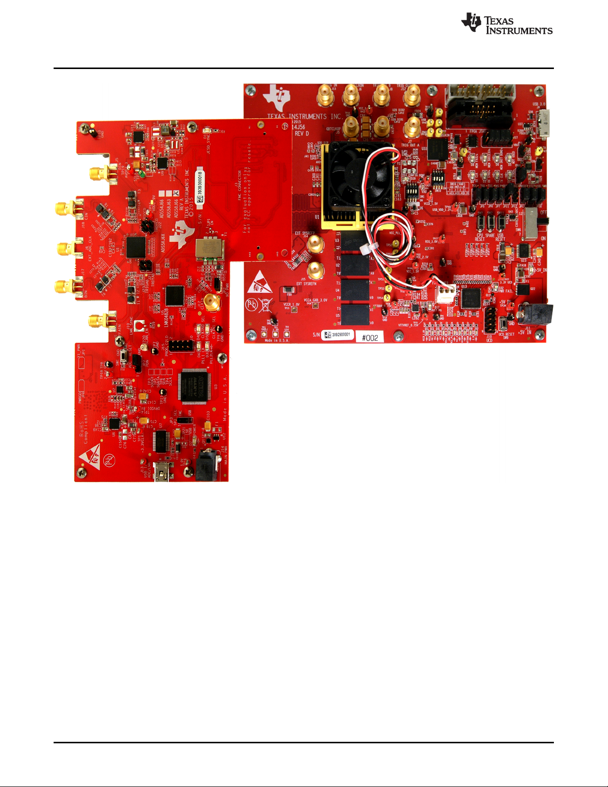
purpose use. Figure 1 shows the TI ADS58J63EVM plugged into the TSW14J56EVM.
User's Guide
SLWU086C–November 2013–Revised January 2016
Pattern Generator Card User's Guide
SLWU086C–November 2013–Revised January 2016
Submit Documentation Feedback
Copyright © 2013–2016, Texas Instruments Incorporated
TSW14J56 JESD204B High-Speed Data Capture and Pattern Generator
Card User's Guide
1
Page 2
Functionality
www.ti.com
Figure 1. TSW14J56EVM Interfacing with an ADS58J63EVM
The major features of the TSW14J56 are:
• Subclasses: 0 (backward compatible), 1, 2
• Support for deterministic latency
• Serial lanes speeds up to 12.5 Gbps
• 10 routed transceiver channels
• 32 Gb DDR3 SDRAM (split into four independent 512×164 Gb SDRAMs, total of 512M samples each).
Quarter rate DDR3 controllers supporting up to 800-MHz operation
• 256K 16-bit samples of internal FPGA memory
• Supports 1.8, 2.5 and 3-V adjustable CMOS IO standard
• Option for general purposed 10 MH oscillator
• Onboard UCD90120A for power sequencing and monitoring
• Onboard Cypress CYUSB301X USB 3.0 device for JTAG and parallel interface to the FPGA
• Reference clocking for transceivers available through FMC port or SMAs
• Supported by TI HSDC PRO software
• FPGA firmware developed with Quartus II 14.0 and QSYS
2
TSW14J56 JESD204B High-Speed Data Capture and Pattern Generator
Card User's Guide
Copyright © 2013–2016, Texas Instruments Incorporated
SLWU086C–November 2013–Revised January 2016
Submit Documentation Feedback
Page 3
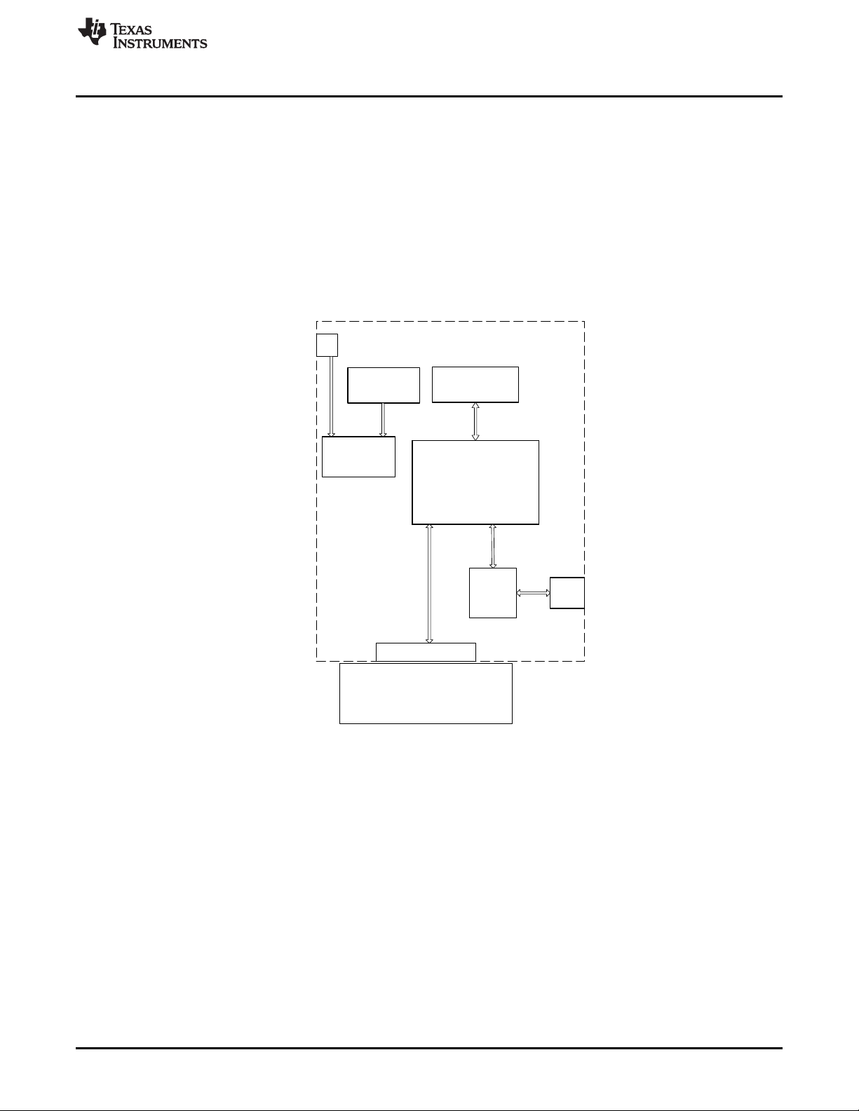
+5 VDC Input
32Gb DDR III
RAM
ALTERA
Arria V GZ
(Firmware)
USB
to
Parallel
32 Bit 100 MHz
Parallel Interface
USB 3.0
Port
TSW14J56 EVM
ADC or DAC EVM
FMC Connector
JESD204B Interface
Data, Device CLK,
SYSREF, SYNC, GPIO
Power Sequencer/
Monitor
LDO and Switch
Regulators
www.ti.com
Figure 2 shows a block diagram of the TSW14J56 EVM.
Functionality
– JESD RX IP core with support for:
• USB and JTAG reconfigurable JESD core parameters: L, M, K, F, HD, S, and more
• ILA configuration data accessible through USB and JTAG
• Lane alignment and character replacement enabled or disabled through USB and JTAG
– JESD TX IP core with support for:
• USB and JTAG reconfigurable JESD core parameters: L, M, K, F, HD, S, and more
• ILA data configured through USB and JTAG
• Character replacement enabled or disabled through USB and JTAG
– Dynamically reconfigurable transceiver data rate. Operating range from 0.600 to 12.5 Gbps
Figure 2. TSW14J56 EVM Block Diagram
1.1 ADC EVM Data Capture
New TI high-speed ADCs and DACs now have high-speed serial data that meets the JESD204B standard.
These devices are generally available on an EVM that connects directly to the TSW14J56EVM. The
common connector between the EVMs and the TSW14J56EVM is a Samtec high-speed, high-density
FMC connector (SEAF-40-05.0-S-10-2-A-K) suitable for high-speed differential pairs up to 21 Gbps. A
common pinout for the connector across a family of EVMs has been established. At present, the interface
between the EVMs and the TSW14J56EVM has defined connections for 10 lanes of serial differential
data, two device clock pairs, two JESD204B SYSREF and SYNC pairs. There are four over-range singleended indicators, 12 spare general purpose CMOS I/O pins, and 29 spare differential LVDS or 58 singleended CMOS signals. The board has a spare SMA interface to the FPGA, 4 spare dip switches, a
pushbutton switch, several spare test points routed to the FPGA and 8 status LED's.
SLWU086C–November 2013–Revised January 2016
Submit Documentation Feedback
Copyright © 2013–2016, Texas Instruments Incorporated
TSW14J56 JESD204B High-Speed Data Capture and Pattern Generator
Card User's Guide
3
Page 4

Functionality
The data format for JESD204B ADCs and DACs is a serialized format, where individual bits of the data
are presented on the serial pairs commonly referred to as lanes. Devices designed around the JESD204B
spec can have up to 8 lanes for transmitting or receiving data. The firmware in the FPGA on the
TSW14J56 is designed to accommodate any of TI's ADC or DAC operating with any number of lanes from
1 to 8.
The GUI loads the FPGA with the appropriate firmware and a specific JESD204B configuration, based on
the ADC device selected in the device drop down window. Each ADC device that appears in this window
has an initialization file (.ini) associated to it. This .ini file contains JESD information, such as number of
lanes, number of converters, octets per frame, and other parameters. This information is loaded into the
FPGA registers after the user clicks on the capture button. After the parameters are loaded,
synchronization is established between the data converter and FPGA and valid data is then captured into
the on-board memory. See the High-Speed Data Capture Pro GUI Software User's Guide SLWU087 and
section 2.3 in the guide for more information. Several .ini files are available to allow the user to load predetermined ADC JESD204B interfaces. For example, if the user selects the ADC called
"ADS42JB69_LMF_421", the FPGA will be configured to capture data from the ADS42JB69EVM with the
ADC JESD interface configured for 4 lanes, 2 converters, and 1 octet per frame.
The TSW14J56 device can capture up to 2G 16-bit samples at a maximum line rate of 12.5 Gbps that are
stored inside the on-board DDR3 memory. To acquire data on a host PC, the FPGA reads the data from
memory and transmits parallel data to the on-board high-speed parallel-to-USB converter.
1.2 DAC EVM Pattern Generator
In pattern generator mode, the TSW14J56EVM generates desired test patterns for DAC EVMs under test.
These patterns are sent from the host PC over the USB interface to the TSW14J56. The FPGA stores the
data received into the on-board DDR3 memory. The data from the memory is then read by the FPGA,
converted to JESD204B serial format, then transmitted to a DAC EVM. The TSW14J56 can generate
patterns up to 2G 16-bit samples at a line rate up to 12.5 Gbps.
The GUI comes with several existing test patterns that can be download immediately. The GUI also has a
pattern generation tool that allows the user to generate a custom pattern, then download it to the on-board
memory. See the High-Speed Data Capture Pro Software User's Guide SLWU087 for more information.
Like the ADC capture mode, the DAC pattern generator mode uses .ini files to load predetermined
JESD204B interface information to the FPGA.
www.ti.com
2 Hardware Configuration
This section describes the various portions of the TSW14J56EVM hardware.
2.1 Power Connections
The TSW14J56EVM hardware is designed to operate from a single supply voltage of +5 V DC. The power
input is controlled by the on and off switch, SW6. Make sure this switch is in the off position before
inserting the provided power cable. Insert the connector end of the power cable into J11 of the EVM.
Connect the positive red wire end of the power cable to +5V +/- 0.3VDC output of a +5VDC power supply
rated for at least 3 Amps. Connect the negative black wire to the RETURN or GND of the power supply.
The board can also be powered up by providing +5 V DC to the red test point, TP34, and the return to any
black GND test point. The TSW14J56 draws approximately 0.6 A at power-up and 1.6 A when capturing 4
lanes of data from an ADS42JB69EVM at a line rate of 2.5 Gpbs.
4
TSW14J56 JESD204B High-Speed Data Capture and Pattern Generator
Card User's Guide
SLWU086C–November 2013–Revised January 2016
Copyright © 2013–2016, Texas Instruments Incorporated
Submit Documentation Feedback
Page 5
www.ti.com
2.2 Switches, Jumpers, and LEDs
2.2.1 Switches and Pushbuttons
The TSW14J56 contains several switches and pushbuttons that enable certain functions on the board.
The description of the switches can be found in Table 1.
Table 1. Switch Description of the TSW14J56 Device
Component Description
SW6 Board main power switch
SW1 Spare dip switches that are connected to spare FPGA inputs
SW2 Spare pushbutton that are connected to spare FPGA inputs
SW7 (CPU RESET) FPGA hardware reset
SW10 Dip switch to set VAR adjustable regulator output voltage. Default is 1.8V
(switches 1,3,4 off, 2 on)
SW11 USB hardware reset
SW9 (UCD Reset) Power monitor U13 reset
2.2.2 Jumpers
The TSW14J56 contains several jumpers (JP) and solder jumpers (SJP) that enable certain functions on
the board. The description of the jumpers can be found in Table 2.
Hardware Configuration
Table 2. Jumper Description of the TSW14J56 Device
Component Description Default
SJP1 Power enable to general purpose 10-MHz oscillator Y1 1 to 2
SJP19 - SJP21 Address for spare I2C controller U42 2 to 3
SJ14, SJ15, SJ18 Sets programming mode for FPGA 2 to 3
SJ16, SJ17 Sets programming mode for FPGA 1 to 2
JP4, JP5, JP6, and JP7 USB or JTAG control of FPGA programming. Default is USB control 2 to 3
JP16
JP14 5-V supply for U39. Default is no power Not installed
JP15 U39 output used for power. Default is disabled Not installed
JP17 U39 enable. 2 to 3
SJP2, SJP3 Direction control for buffer U29. Default is B to A 2 to 3
SJP9 Direction control for buffer U30. Default is B to A 2 to 3
SJP10, SJP11 Direction control for buffer U41. Default is B to A 2 to 3
SJP12, SJ13 Direction control for buffer U28. Default is B to A 2 to 3
JP11 Programming mode for USB controller U33 1 to 2
JP12 Programming mode for USB controller U33 Not installed
JP13 Programming mode for USB controller U33 2 to 3
JP10 USB TCK routing option 2 to 3
J17 USB Controller U33 to Flash U36 interface. 3 to 4, 5 to 6, 7 to 8, 9 to 10
USB cable or internal 5-V power for USB interface. Default is USB
cable power
2 to 3
SLWU086C–November 2013–Revised January 2016
Submit Documentation Feedback
Copyright © 2013–2016, Texas Instruments Incorporated
TSW14J56 JESD204B High-Speed Data Capture and Pattern Generator
Card User's Guide
5
Page 6

Hardware Configuration
2.3 LEDs
2.3.1 Power and Configuration LEDs
Several LEDs are on the TSW14J56 EVM to indicate the presence of power and the state of the FPGA.
The description of these LEDs can be found in Table 3.
Table 3. Power and Configuration LED Description of the TSW14J56 Device
Component Description
D17 On if DDR3 VREF power is good
D10 On if 5V board power is present
D32 On if power monitor device indicates that a power net is out of tolerance
D11 On if +1.0 V is within specification
D13 On if VCCD_1.5 V is within specification
D16 On if VCC_1.5 V is within specification
D21 On if VCC_2.5 V is within specification
D23 On if VCCA_GXB_3.0 V is within specification
D25 On if VCC_PLL_2.5 V is within specification
D26 On if VCC_0.85V is within specification
D27 On if VCCDDR_1.5 V is within specification
D30 On if VTTDDR_0.75 V is within specification
D34 On if VAR power is present
D33 On if USB_1.2 V is within specification
D28 On after FPGA completes configuration
www.ti.com
2.3.2 Status LEDs
Eight status LEDs on the TSW14J56EVM indicate the status of the FPGA, DDR3, and JESD204B
interface:
D1 – Indicates DAC EVM established SYNC with the TSW14J56 device when off
D2 – Indicates presence of device clock from DAC EVM when blinking
D3 – Indicates ADC EVM established SYNC with the TSW14J56 device when off
D4 – Indicates presence of device clock from ADC EVM when blinking
D5 – Not used
D6 – DDR3 initialization and calibration complete when off
D7 – DDR3 ready when off
D8 – DDR3 pass calibration and initialization if on
2.3.3 Connectors
2.3.3.1 SMA Connectors
The TSW14J56 has 9 SMA connectors. The connectors are defined below:
J6 GBTCLK0N Spare Transceiver reference clock negative input
J5 GBTCLK0P Spare Transceiver reference clock positive input
J13 TRIG_IN Adjustable level CMOS trigger input. Default level is 1.8 V
J7 TRIG_OUT_A Adjustable level CMOS trigger output. Default level is 1.8 V
J8 TRIG_OUT_B Adjustable level CMOS trigger output. Default level is 1.8 V
6
TSW14J56 JESD204B High-Speed Data Capture and Pattern Generator
Card User's Guide
Copyright © 2013–2016, Texas Instruments Incorporated
SLWU086C–November 2013–Revised January 2016
Submit Documentation Feedback
Page 7

www.ti.com
J12 TRIG_OUT_C Adjustable level CMOS trigger output. Default level is 1.8 V
J3 REF_OSC_IN AC coupled spare input connected to FPGA CLK input
J14 EXT_SYSREFP Spare SYSREF positive input to FPGA
J15 EXT_SYSREFN Spare SYSREF negative input to FPGA
2.3.3.2 FPGA Mezzanine Card (FMC) Connector
The TSW14J56 EVM has one connector to allow for the direct plug in of TI JESD204B serial interface
ADC and DAC EVMs. The specifications for this connector are mostly derived from the ANSI/VITA 57.1
FPGA Mezzanine Card (FMC) Standard. This standard describes the compliance requirements for a lowoverhead protocol bridge between the IO of a mezzanine card and an FPGA processing device on a
carrier card. This specification is being used by FPGA vendors on their development platforms.
The FMC connector, J4, provides the interface between the TSW14J56EVM and the ADC or DAC EVM
under test. This 400-pin Samtec high-speed, high-density connector (part number SEAF-40-05.0-S-10-2A-K) is suitable for high-speed differential pairs up to 21 Gbps.
In addition to the JESD204B standard signals, several CMOS single-ended signals and LVDS differential
signals are connected between the FMC and FPGA. In the future, these signals may allow the HSDC Pro
GUI to control the SPI serial programming of ADC and DAC EVMs that support this feature. The
connector pinout description is shown in Table 4.
Table 4. FMC Connector Description of the TSW14J56
Hardware Configuration
FMC Signal Name FMC Pin Standard JESD204
Application Mapping
RX0_P/N C6 and C7 Lane 0± (M → C) JESD Serial data transmitted from mezzanine and received
by carrier
RX1_P/N A2 and A3 Lane 1± (M → C) JESD Serial data transmitted from mezzanine and received
by carrier
RX2_P/N A6 and A7 Lane 2± (M → C) JESD Serial data transmitted from mezzanine and received
by carrier
RX3_P/N A10 and A11 Lane 3± (M → C) JESD Serial data transmitted from mezzanine and received
by carrier
RX4_P/N A14 and A15 Lane 4± (M → C) JESD Serial data transmitted from mezzanine and received
by carrier
RX5_P/N A18 and A19 Lane 5± (M → C) JESD Serial data transmitted from mezzanine and received
by carrier
RX6_P/N B16 and B17 Lane 6± (M → C) JESD Serial data transmitted from mezzanine and received
by carrier
RX7_P/N B12 and B13 Lane 7± (M → C) JESD Serial data transmitted from mezzanine and received
by carrier
RX8_P/N B8 and B9 Lane 8± (M → C) JESD Serial data transmitted from mezzanine and received
by carrier
RX9_P/N B4 and B5 Lane 9± (M → C) JESD Serial data transmitted from mezzanine and received
by carrier
TX0_P/N C2 and C3 Lane 0± (C → M) JESD Serial data transmitted from carrier and received by
mezzanine
TX1_P/N A22 and A23 Lane 1± (C → M) JESD Serial data transmitted from carrier and received by
mezzanine
TX2_P/N A26 and A27 Lane 2± (C → M) JESD Serial data transmitted from carrier and received by
mezzanine
TX3_P/N A30 and A31 Lane 3± (C → M) JESD Serial data transmitted from carrier and received by
mezzanine
TX4_P/N A34 and A35 Lane 4± (C → M) JESD Serial data transmitted from carrier and received by
mezzanine
TX5_P/N A38 and A39 Lane 5± (C → M) JESD Serial data transmitted from carrier and received by
mezzanine
Description
SLWU086C–November 2013–Revised January 2016
Submit Documentation Feedback
Copyright © 2013–2016, Texas Instruments Incorporated
TSW14J56 JESD204B High-Speed Data Capture and Pattern Generator Card
User's Guide
7
Page 8

Hardware Configuration
FMC Signal Name FMC Pin Standard JESD204
TX6_P/N B36 and B37 Lane 6± (C → M) JESD Serial data transmitted from carrier and received by
TX7_P/N B32 and B33 Lane 7± (C → M) JESD Serial data transmitted from carrier and received by
TX8_P/N B28 and B29 Lane 8± (C → M) JESD Serial data transmitted from carrier and received by
TX9_P/N B24 and B25 Lane 9± (C → M) JESD Serial data transmitted from carrier and received by
GBTCLK0_M2C_P/N D4 and D5 DEVCLKA± (M → C) Primary carrier-bound reference clock required for FPGA
GBTCLK1_M2C_P/N B20 and B21 Alt. DEVCLKA± (M → C) Alternate Primary Carrier-bound reference clock required for
CLK_LA0_P/N G6 and G7 DEVCLKB± (M → C) Secondary carrier-bound device clock. Used for special FPGA
LA01_P/N_CC D8 and D9 DEVCLK± (C → M) Mezzanine-bound device clock. Used for low noise
SYSREF_P/N G9 and G10 SYSREF± (M → C) Carrier-bound SYSREF signal
LA05_P/N D11 and D12 SYSREF± (C → M) Mezzanine-bound SYSREF signal
RX_SYNC_P/N G12 and G13 SYNC± (C → M) ADC mezzanine-bound SYNC signal for use in class 0/1/2
TX_SYNC_P/N F10 and F11 DAC SYNC± (M → C) Carrier-bound SYNC signal for use in class 0/1/2 JESD204
TX_ALT_SYNC_P/N F19 and F20 Alt. DAC SYNC± (M → C) Alternate carrier-bound SYNC signal for use in class 0/1/2
RX_ALT_SYNC_P/N H31 and H32 Alt. SYNC± (C → M) Alternate ADC mezzanine-bound SYNC signal. For use when
SYNC K22 DAC SYNC (M → C) Carrier-bound CMOS-level SYNC signal for use in class 0/1/2
PG_M2C_A F1 Power good from mezzanine to carrier
CLK0_M2C_P/N H4 and H5 GPIO clock
CLK1_M2C_P/N G2 and G3 GPIO clock
www.ti.com
Table 4. FMC Connector Description of the TSW14J56 (continued)
Description
Application Mapping
mezzanine
mezzanine
mezzanine
mezzanine
giga-bit transceivers. Equivalent to device clock.
FPGA giga-bit transceivers. For use when DEVCLKA (M →
C) is not available
Device Clock, SYSREF, and SYNC
functions such as sampling SYSREF
conversion clock
JESD204 systems
systems
JESD204B systems
SYNC (C → M) is not available
JESD204 systems
Special Purpose I/O
All other signals not mentioned in Table 4 can be used as general purpose I/O, either as single-ended
signals or differential pairs. The ANSI/VITA 57.1 standard assigns voltages to certain pins. These are
labeled as 12V, 3P3V, and VADJ nets on the connector page of the schematic. On the TSW14J56, these
pins are connected to test points to allow the user to provide voltages at these pin locations.
8
TSW14J56 JESD204B High-Speed Data Capture and Pattern Generator
Card User's Guide
Copyright © 2013–2016, Texas Instruments Incorporated
SLWU086C–November 2013–Revised January 2016
Submit Documentation Feedback
Page 9

www.ti.com
2.3.3.3 JTAG Connectors
The TSW14J56EVM includes three industry-standard JTAG connectors; one that connects to the JTAG
ports of the FPGA, one that connects to the JTAG pins of the Cypress FX3 USB Contoller and the other
that connects to the programming pins of the power monitor/sequencer device. Jumpers on the
TSW14J56EVM allow for the FPGA to be programmed from the JTAG connector or the USB interface.
JTAG connectors J2, J10 and J16 are to be used for troubleshooting only. The board default setup is with
the FPGA JTAG pins connected to JTAG connector J16. The FPGA can be programmed using this
connector if the MSEL inputs are set to the proper logic levels. These are set by solder jumpers SJP14-
18. Consult the Altera data sheet for more information regarding JTAG programming. The FPGA also has
the parallel programming inputs connected to the USB 3.0 controller. With SJP14-18 in teh default
postions, this allows the FPGA to be programmed by the HSDC Pro software GUI. Every time the
TSW14J56EVM is powered-down, the FPGA configuration is removed. The user must program the FPGA
through the GUI after every time the board is powered-up. J2 can be used to program the USB controller
U33. This device is programmed at power-up using the factory pre-programmed flash device U36. JTAG
connector J10 is used to program the TI UCD90120A power monitor/sequencer device. This device is preprogrammed at the factory and this interface should only be used for troubleshooting.
2.3.3.4 USB I/O Connection
Control of the TSW14J56EVM is through USB 3.0 connector J9. This provides the interface between
HSDC Pro GUI running on a PC Windows™ operating system and the FPGA. For the computer, the
drivers needed to access the USB port are included on the HSDC Pro GUI installation software that can
be downloaded from the web. The drivers are automatically installed during the installation process. On
the TSW14J56EVM, the USB port is used to identify the type and serial number of the EVM under test,
load the desired FPGA configuration file, capture data from ADC EVMs, and send test pattern data to the
DAC EVMs.
Hardware Configuration
SLWU086C–November 2013–Revised January 2016
Submit Documentation Feedback
Copyright © 2013–2016, Texas Instruments Incorporated
TSW14J56 JESD204B High-Speed Data Capture and Pattern Generator
Card User's Guide
9
Page 10

Software Start-Up
3 Software Start-Up
3.1 Installation Instructions
Download the latest version of the HSDC Pro GUI (slwc107x.zip) to a local location on a host PC. Visit
www.ti.com and find the install link on the TSW14J56EVM page.
Unzipping the software package generates a folder called “High Speed Data Converter Pro - Installer
vx.xx.exe", where x.xx is the version number. Run this program to start the installation.
Follow the on-screen instructions during installation.
NOTE: If an older version of the GUI has already been installed, make sure to uninstall it before
loading a newer version.
www.ti.com
Make sure to disconnect all USB cables from any TSW14xxx boards before installing the software.
Follow all on-screen instructions. Accept the license agreements. After the installer has finished, click
“Next”.
The GUI executable and associated files reside in the following directory: C:\Program Files (x86)\Texas
Instruments\High Speed Data Converter Pro.
3.2 USB Interface and Drivers
• Connect a USB 3.0 cable between J9 of the TSW14J56EVM and a host PC.
• Connect the provided power cable between the EVM and a +5 VDC source.
• Set SW6 to on.
Click on the High-Speed Data Converter Pro icon that was created on the desktop panel, or go to
C:\Program Files (x86)\Texas Instruments\High Speed Data Converter Pro and double click on the
executable called “High Speed Data Converter Pro.exe” to start the GUI.
The GUI first attempts to connect to the EVM USB interface. If the GUI identifies a valid board serial
number, a pop-up opens displaying this value, as shown in Figure 4. The user can connect several
TSW14J56 EVMs to one host PC, but the GUI can only connect to one at a time. When multiple boards
are connected to the PC, the pop-up displays all of the serial numbers found. The user then selects which
board to associate the GUI with.
Figure 3. GUI Installation
10
TSW14J56 JESD204B High-Speed Data Capture and Pattern Generator
Card User's Guide
Copyright © 2013–2016, Texas Instruments Incorporated
SLWU086C–November 2013–Revised January 2016
Submit Documentation Feedback
Page 11

www.ti.com
Click “OK” to connect the GUI to the board. The top level GUI opens and appears as shown in Figure 5.
Software Start-Up
Figure 4. TSW14J56EVM Serial Number
Figure 5. High-Speed Data Converter Pro GUI Top Level
If the message “No Board Connected” opens, double check the USB cable connections and that power
switch SW6 is in the on position. Remove the USB cable from the board then re-install. Click on the
“Instrument Option” tab at the top left of the GUI and selecting “Connect to the Board”. If this still does not
correct this issue, check the status of the host USB port.
When the software is installed and the USB cable is connected to the TSW14J56EVM and the PC, the
TSW14J56 USB 3.0 converter should be located in the Hardware Device Manager under the universal
serial bus controllers as shown in Figure 6 labeled as Cypress FX3 USB StreamerExample Device. When
the USB 3.0 cable is removed, this driver will no longer be visible in the device manager. If the drivers are
present in the device manager window and the software still does not connect, remove the USB 3.0 cable
from the board then reconnect. Attempt to connect to the board. If the problem still exists, cycle power to
the board and repeat the prior steps.
SLWU086C–November 2013–Revised January 2016
Submit Documentation Feedback
Copyright © 2013–2016, Texas Instruments Incorporated
TSW14J56 JESD204B High-Speed Data Capture and Pattern Generator
Card User's Guide
11
Page 12

Downloading Firmware
www.ti.com
Figure 6. Hardware Device Manager
4 Downloading Firmware
The TSW14J56EVM has an Altera Arria V GZ device that requires firmware to be downloaded every time
power is cycled to operate. The firmware files needed are special .rbf formatted files that are provided with
the software package. The files used by the GUI currently reside in the directory called C:\Program Files
(x86)\Texas Instruments\High Speed Data Converter Pro\14J56revD Details\Firmware.
To load a firmware, after the GUI has established connection, click the “Select ADC” window in the top left
of the GUI and select the device to evaluate, for example, ADS42JB69_LMF_421, as shown in Figure 7.
The GUI prompts the user to update the firmware for the ADC. Click "Yes”. The GUI will display the
message "Downloading Firmware, Please Wait". The software now loads the firmware from the PC to the
FPGA, a process that takes about 3 seconds. Once completed, the GUI reports an Interface Type in the
lower right corner and the FPGA_CONF_DONE LED (D28) illuminates along with several of the status
LEDs.
12
Figure 7. Select ADC Firmware to be Loaded
TSW14J56 JESD204B High-Speed Data Capture and Pattern Generator
Card User's Guide
Copyright © 2013–2016, Texas Instruments Incorporated
SLWU086C–November 2013–Revised January 2016
Submit Documentation Feedback
Page 13

www.ti.com
For information regarding the use of the TSW14J56EVM with a TI ADC or DAC JESD204B serial interface
EVM, consult the High-Speed Data Converter Pro GUI User's Guide SLWU087 and the individual EVM
User’s Guide, available on www.ti.com.
If the message appears as shown in Figure 8, verify that all jumpers are in the default position and all
power status LEDs are illuminated. If certain jumpers are not installed in the proper location, the USB 3.0
Controller will not boot from flash memory. If any power status LED is off, there may be a problem with a
power supply on the board, which can prevent the firmware from downloading. Unplug and re-install the
USB connector and try to connect to the board. If this fails, cycle the power switch to re-initialize the
power-up sequencer to try to correct this problem.
Downloading Firmware
Figure 8. Download Firmware Error Message
SLWU086C–November 2013–Revised January 2016
Submit Documentation Feedback
Copyright © 2013–2016, Texas Instruments Incorporated
TSW14J56 JESD204B High-Speed Data Capture and Pattern Generator
Card User's Guide
13
Page 14

Revision History
www.ti.com
Revision History
NOTE: Page numbers for previous revisions may differ from page numbers in the current version.
Changes from B Revision (July 2015) to C Revision ..................................................................................................... Page
• Changed Power Connections section to remove included power supply.......................................................... 4
• Removed reference to provided +5VDC source in the USB Interface and Drivers section.................................... 10
Revision History
Changes from A Revision (November 2013) to B Revision ........................................................................................... Page
• Changed TSW14J56EVM Interfacing with an ADS42JB49EVM image............................................................ 2
• Changed TSW14J56 EVM Block Diagram image..................................................................................... 3
• Changed TSW14J56EVM Serial Number image. ................................................................................... 11
• Changed High-Speed Data Converter Pro GUI Top Level image................................................................. 11
• Changed Hardware Device Manager image. ........................................................................................ 12
• Changed Select ADC Firmware to be Loaded image............................................................................... 12
• Changed Download Firmware Error Message image............................................................................... 13
Revision History
Changes from Original (November 2013) to A Revision ................................................................................................ Page
• Added the number of converters and octets........................................................................................... 1
• Added a link to the High-Speed Data Converter Pro GUI ........................................................................... 1
14
Revision History
SLWU086C–November 2013–Revised January 2016
Copyright © 2013–2016, Texas Instruments Incorporated
Submit Documentation Feedback
Page 15

IMPORTANT NOTICE FOR TI DESIGN INFORMATION AND RESOURCES
Texas Instruments Incorporated (‘TI”) technical, application or other design advice, services or information, including, but not limited to,
reference designs and materials relating to evaluation modules, (collectively, “TI Resources”) are intended to assist designers who are
developing applications that incorporate TI products; by downloading, accessing or using any particular TI Resource in any way, you
(individually or, if you are acting on behalf of a company, your company) agree to use it solely for this purpose and subject to the terms of
this Notice.
TI’s provision of TI Resources does not expand or otherwise alter TI’s applicable published warranties or warranty disclaimers for TI
products, and no additional obligations or liabilities arise from TI providing such TI Resources. TI reserves the right to make corrections,
enhancements, improvements and other changes to its TI Resources.
You understand and agree that you remain responsible for using your independent analysis, evaluation and judgment in designing your
applications and that you have full and exclusive responsibility to assure the safety of your applications and compliance of your applications
(and of all TI products used in or for your applications) with all applicable regulations, laws and other applicable requirements. You
represent that, with respect to your applications, you have all the necessary expertise to create and implement safeguards that (1)
anticipate dangerous consequences of failures, (2) monitor failures and their consequences, and (3) lessen the likelihood of failures that
might cause harm and take appropriate actions. You agree that prior to using or distributing any applications that include TI products, you
will thoroughly test such applications and the functionality of such TI products as used in such applications. TI has not conducted any
testing other than that specifically described in the published documentation for a particular TI Resource.
You are authorized to use, copy and modify any individual TI Resource only in connection with the development of applications that include
the TI product(s) identified in such TI Resource. NO OTHER LICENSE, EXPRESS OR IMPLIED, BY ESTOPPEL OR OTHERWISE TO
ANY OTHER TI INTELLECTUAL PROPERTY RIGHT, AND NO LICENSE TO ANY TECHNOLOGY OR INTELLECTUAL PROPERTY
RIGHT OF TI OR ANY THIRD PARTY IS GRANTED HEREIN, including but not limited to any patent right, copyright, mask work right, or
other intellectual property right relating to any combination, machine, or process in which TI products or services are used. Information
regarding or referencing third-party products or services does not constitute a license to use such products or services, or a warranty or
endorsement thereof. Use of TI Resources may require a license from a third party under the patents or other intellectual property of the
third party, or a license from TI under the patents or other intellectual property of TI.
TI RESOURCES ARE PROVIDED “AS IS” AND WITH ALL FAULTS. TI DISCLAIMS ALL OTHER WARRANTIES OR
REPRESENTATIONS, EXPRESS OR IMPLIED, REGARDING TI RESOURCES OR USE THEREOF, INCLUDING BUT NOT LIMITED TO
ACCURACY OR COMPLETENESS, TITLE, ANY EPIDEMIC FAILURE WARRANTY AND ANY IMPLIED WARRANTIES OF
MERCHANTABILITY, FITNESS FOR A PARTICULAR PURPOSE, AND NON-INFRINGEMENT OF ANY THIRD PARTY INTELLECTUAL
PROPERTY RIGHTS.
TI SHALL NOT BE LIABLE FOR AND SHALL NOT DEFEND OR INDEMNIFY YOU AGAINST ANY CLAIM, INCLUDING BUT NOT
LIMITED TO ANY INFRINGEMENT CLAIM THAT RELATES TO OR IS BASED ON ANY COMBINATION OF PRODUCTS EVEN IF
DESCRIBED IN TI RESOURCES OR OTHERWISE. IN NO EVENT SHALL TI BE LIABLE FOR ANY ACTUAL, DIRECT, SPECIAL,
COLLATERAL, INDIRECT, PUNITIVE, INCIDENTAL, CONSEQUENTIAL OR EXEMPLARY DAMAGES IN CONNECTION WITH OR
ARISING OUT OF TI RESOURCES OR USE THEREOF, AND REGARDLESS OF WHETHER TI HAS BEEN ADVISED OF THE
POSSIBILITY OF SUCH DAMAGES.
You agree to fully indemnify TI and its representatives against any damages, costs, losses, and/or liabilities arising out of your noncompliance with the terms and provisions of this Notice.
This Notice applies to TI Resources. Additional terms apply to the use and purchase of certain types of materials, TI products and services.
These include; without limitation, TI’s standard terms for semiconductor products http://www.ti.com/sc/docs/stdterms.htm), evaluation
modules, and samples (http://www.ti.com/sc/docs/sampterms.htm).
Mailing Address: Texas Instruments, Post Office Box 655303, Dallas, Texas 75265
Copyright © 2018, Texas Instruments Incorporated
Page 16

Mouser Electronics
Authorized Distributor
Click to View Pricing, Inventory, Delivery & Lifecycle Information:
Texas Instruments:
TSW14J56EVM
 Loading...