

Page 1
ADS EVM
TSW1405
TI TSW1405 High-Speed ADC
Evaluation Board
HDL User’s Guide
May 2012 Reference Design RD1127
Introduction
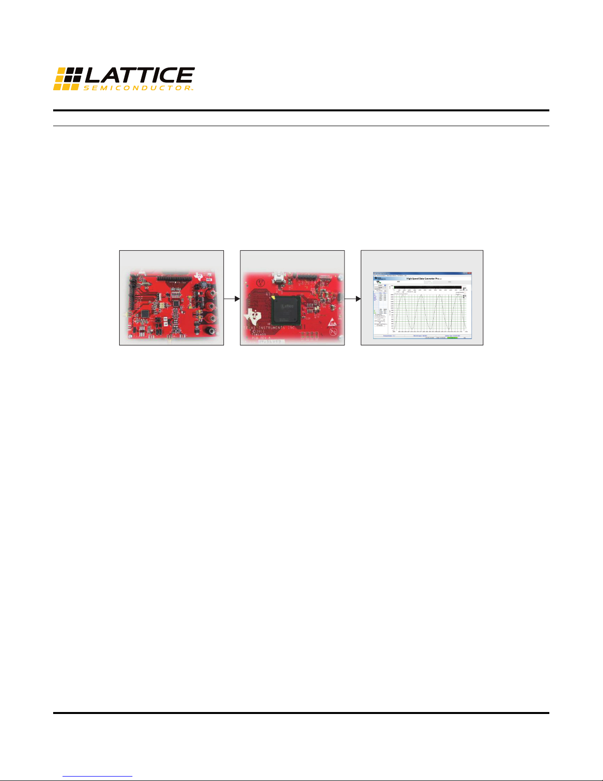
The TSW1405EVM Low Cost Data Capture Card from Texas Instruments (TI) assists designers in prototyping and
evaluating the performance of high-speed ADCs that feature parallel/serial LVDS outputs. The evaluation module
features a powerful LatticeECP3™-35 FPGA. The FPGA can be used as a flexible and rapid prototyping environment for digital design, interfacing directly to the LVDS output of the TI ADC under evaluation. This HDL reference
design is available for users to get started with the evaluation board and capture ADC data using the TI High Speed
Data Converter Pro software.
Figure 1. Hardware Evaluation Overview
High Speed Data Converter Pro
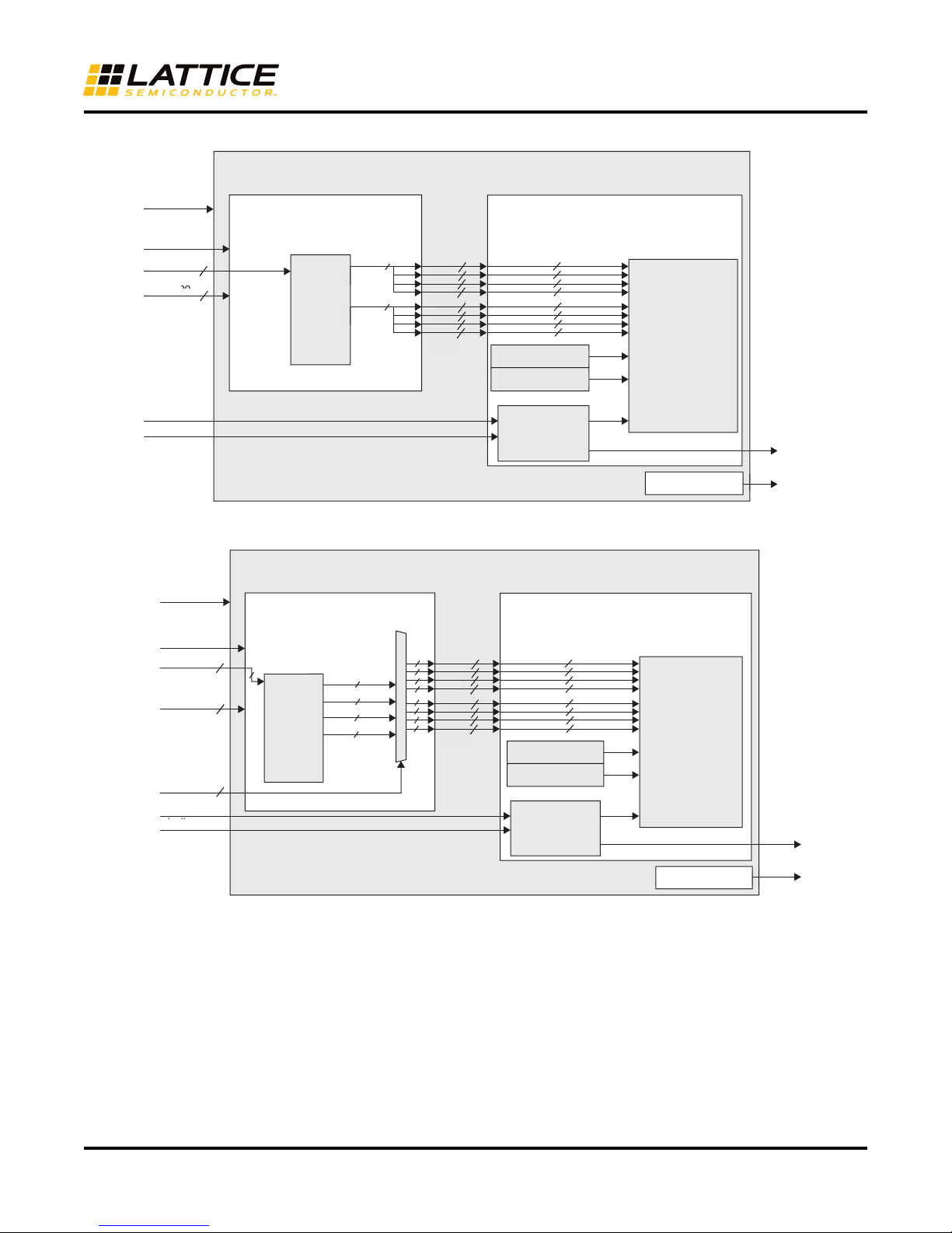
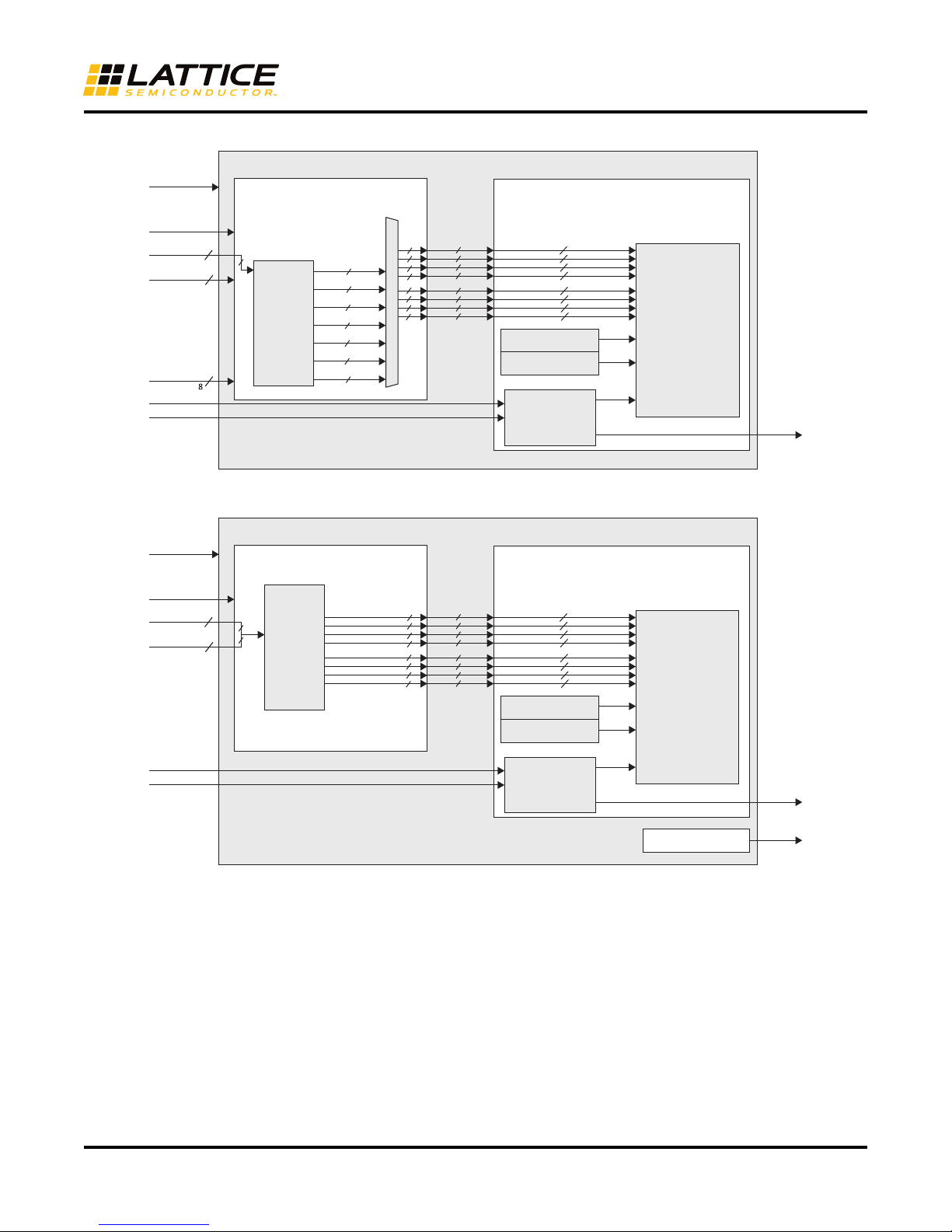
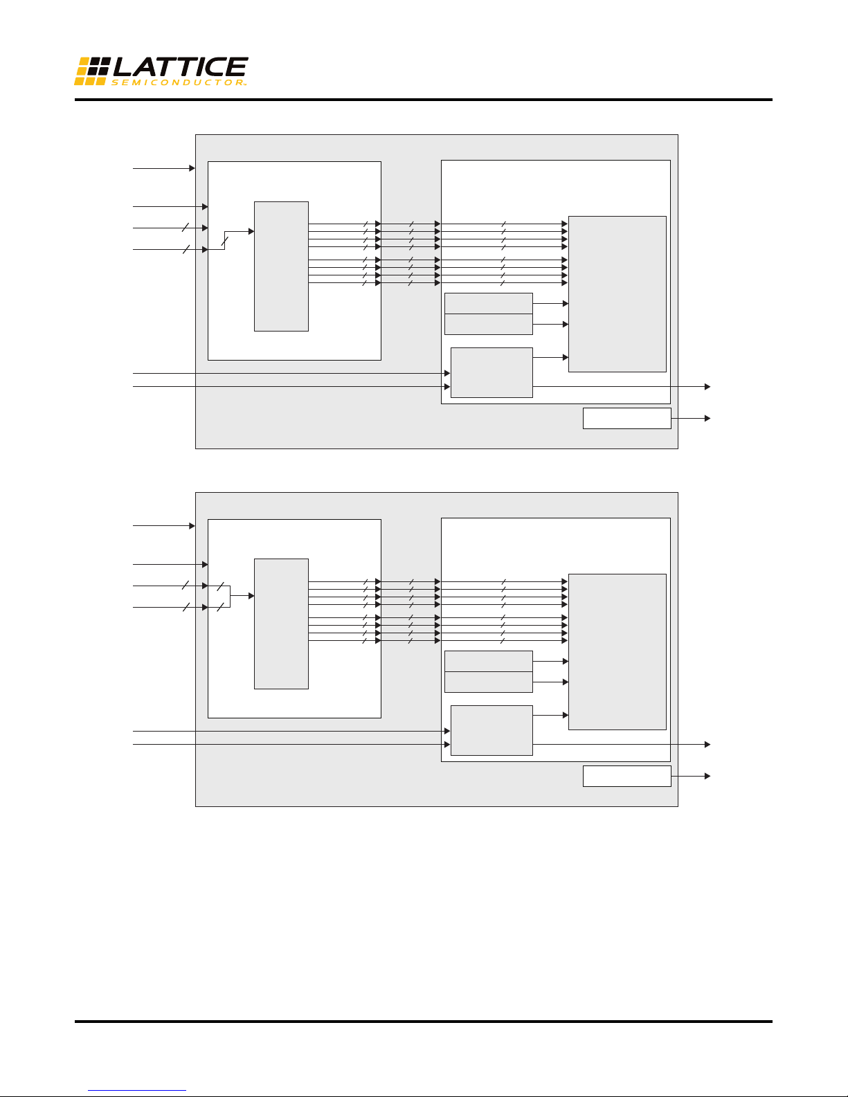
Currently, HDL reference designs targeting the LatticeECP3 device support the following TI device families:
• ADS41xx and ADS61xx single channel
• ADS62Pxx and ADS42xx dual channel
• ADS58C48 four channel
• ADS5400 dual bus
• ADS5463 single channel
• ADS5485 single channel
The HDL reference designs for these converters contain two primary modules for capturing the LVDS data from the
ADC.
• ADCIF – Contains the I/O logic and gearing functions for the LVDS pins. It also converts the double data rate
(DDR) input channel to a single data rate (SDR) parallel bus.
• DUMPMEM_TOP – Stores the channel’s parallel data to internal DPRAM. The ADC data extracts a SPI controller within the module. The High Speed Data Converter Pro software can import the data from this controller
through the USB port.
ADCIF module is the only design block required if the user desires to implement their own design using the
ADS41xx/ADS61xx, ADS62Pxx/ADS42xx, ADS58C48, ADS5400, ADS5463, ADS5485 with the LatticeECP3
device. The top level design instantiates the primary modules and connects them together. It also contains a LED
blinker circuit. This circuit flashes the LED when the LVDS clock output from the ADC is running and is available to
the FPGA. Figures 2 to 7 show the block diagrams for each respective ADC design.
© 2012 Lattice Semiconductor Corp. All Lattice trademarks, registered trademarks, patents, and disclaimers are as listed at www.latticesemi.com/legal. All other brand
or product names are trademarks or registered trademarks of their respective holders. The specifications and information herein are subject to change without notice.
www.latticesemi.com 1 rd1127_01.2
Page 2
TI TSW1405 High-Speed ADC Evaluation Board
TSW1405_1ch_bit_wise
ADCIF
DUMPMEM_TOP
clk_lvds_rx_p
lvds_rx_port0
lvds_rx_port1
17
12
iDDRx2
{[12:9], [7:4]}
sample 0
sample 1
[15:0]
[15:0]
16
16
16
16
16
16
16
16
16
DUMPMEM_DP
DUMPMEM_SPI
DUMPMEM_WCTRL
DUMPMEM_RCTRL
spi_miso
spi_clk
spi_ss
reset_n
LED
ADC Clock Counter
TSW1405_2ch_bit_wise
DUMPMEM_TOP
clk_lvds_rx_p
lvds_rx_port0
lvds_rx_port1
17
12
{[15:9], [7:1]}
16
16
16
16
16
16
16
16
spi_miso
spi_clk
spi_ss
reset_n
LED
[13:0]
[13:0]
[13:0]
[13:0]
sample 0 chan 0
sample 1 chan 0
sample 0 chan 1
sample 1 chan 1
cap_chans
8
ADCIF
DUMPMEM_DP
DUMPMEM_WCTRL
DUMPMEM_RCTRL
DUMPMEM_SPI
ADC Clock Counter
iDDRx2
Figure 2. Single Channel ADC Block Diagram (ADS41xx/ADS61xx)
HDL User’s Guide
Figure 3. Dual Channel ADC Block Diagram (ADS62Pxx/ADS42xx)
ort1
2
Page 3
TI TSW1405 High-Speed ADC Evaluation Board
TSW1405_2ch_bit_wise
ADCIF
DUMPMEM_TOP
17
12
sample 0, chan 0
16
sample 1, chan 0
sample 0, chan 1
sample 1, chan 1
sample 0, chan 2
sample 1, chan 2
sample 0, chan 3
[11:0]
[11:0]
[11:0]
[11:0]
[11:0]
[11:0]
[11:0]
iDDRx2
DUMPMEM_DP
DUMPMEM_SPI
DUMPMEM_WCTRL
DUMPMEM_RCTRL
spi_miso
{[28:17], [15:10], [7:2]}
cap_chans
16
16
16
16
16
16
16
clk_lvds_rx_p
lvds_rx_port0
lvds_rx_port1
spi_clk
spi_ss
reset_n
TSW1405_dual_bus
ADCIF
DUMPMEM_TOP
clk_lvds_rx_p
lvds_rx_port0
12
17
sample 0, chan A
16
sample 0, chan B
sample 1, chan A
sample 1, chan B
sample 2, chan A
sample 2, chan B
sample 3, chan A
sample 3, chan B
lvds_rx_port1
iDDRx2
DUMPMEM_DP
DUMPMEM_SPI
DUMPMEM_WCTRL
DUMPMEM_RCTRL
spi_miso
LED
spi_clk
spi_ss
reset_n
16
16
16
16
16
16
16
ADC Clock Counter
{[11:0], h’40}
{[28:17],
[14:3]}
{[11:0], h’40}
{[11:0], h’40}
{[11:0], h’40}
{[11:0], h’40}
{[11:0], h’40}
{[11:0], h’40}
{[11:0], h’40}
Figure 4. Four Channel ADC Block Diagram (ADS58C48)
Figure 5. Dual Bus ADC Block Diagram (ADS5400)
HDL User’s Guide
3
Page 4
TI TSW1405 High-Speed ADC Evaluation Board
TSW1405_sample_wise
ADCIF
DUMPMEM_TOP
clk_lvds_rx_p
lvds_rx_port0
lvds_rx_port1
12
17
[14:1]
IDDRx2
DUMPMEM_DP
DUMPMEM_SPI
DUMPMEM_WCTRL
DUMPMEM_RCTRL
spi_miso
spi_clk
spi_ss
reset_n
LED
ADC Clock Counter
{[13:0], 4’h0}
{[13:0], 4’h0}
{[13:0], 4’h0}
{[13:0], 4’h0}
{[13:0], 4’h0}
{[13:0], 4’h0}
{[13:0], 4’h0}
{[13:0], 4’h0}
sample 0
sample 0
sample 1
sample 1
sample 2
sample 2
sample 3
sample 3
16
16
16
16
16
16
16
16
TSW1405_1ch_edge_bit_wise
ADCIF
DUMPMEM_TOP
clk_lvds_rx_p
lvds_rx_port0
lvds_rx_port1
12
17
{[12:9], [7:4]}
IDDRx2
DUMPMEM_DP
DUMPMEM_SPI
DUMPMEM_WCTRL
DUMPMEM_RCTRL
spi_miso
spi_clk
spi_ss
reset_n
LED
ADC Clock Counter
{[13:0], 4’h0}
{[13:0], 4’h0}
{[13:0], 4’h0}
{[13:0], 4’h0}
{[13:0], 4’h0}
{[13:0], 4’h0}
{[13:0], 4’h0}
{[13:0], 4’h0}
sample 0
sample 0
sample 1
sample 1
sample 2
sample 2
sample 3
sample 3
16
16
16
16
16
16
16
16
Figure 6. Single Channel ADC Block Diagram (ADS5463)
HDL User’s Guide
Figure 7. Single Channel ADC Block Diagram (ADS5485)
The input of the ADCIF module is the single or dual channel double data rate (DDR) output from the ADC. This
input is converted to two single data rate buses for each channel at half the rate of the ADC input clock. The single
channel design is capable of handling up to eight LVDS DDR inputs from the ADC. The dual channel design is
capable of handling up to seven LVDS DDR inputs for the ADC. Table 2 describes the ADCIF I/O for single and dual
channel designs.
4
Page 5
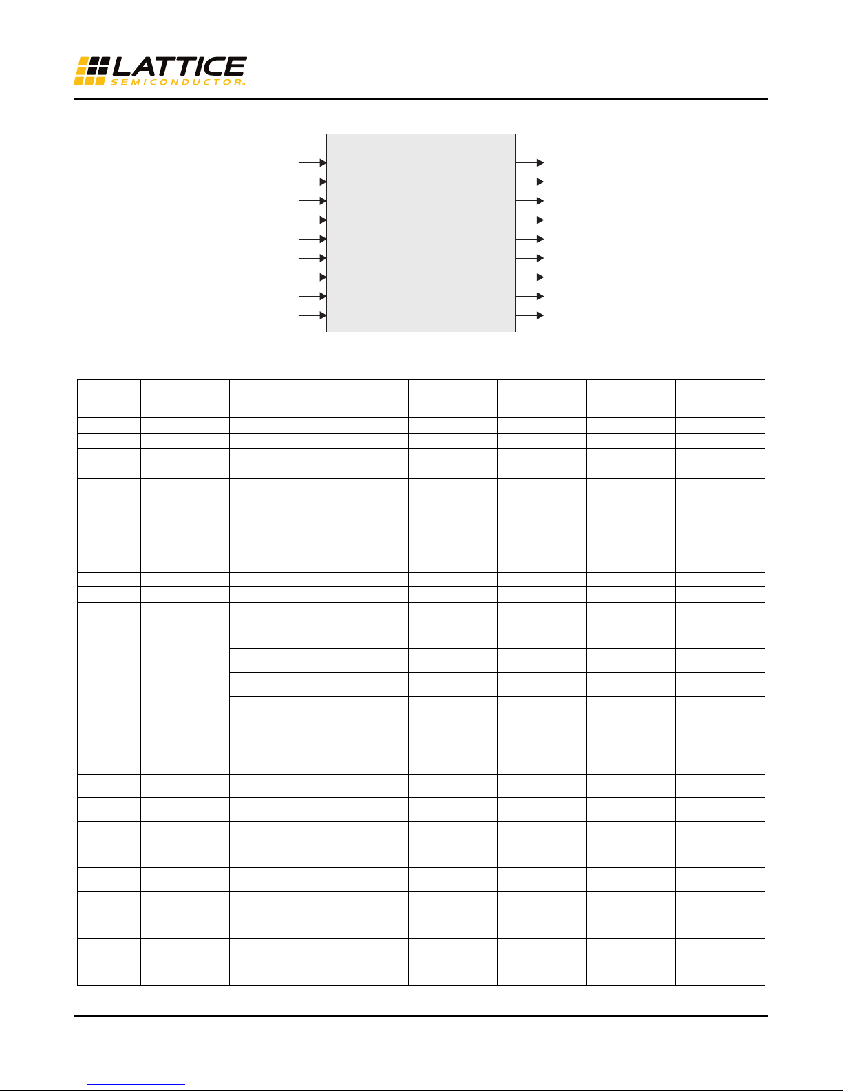
Figure 8. ADCIF Module
clk_adc
dout1[15:0]
dout2[15:0]
dout3[15:0]
dout4[15:0]
dout5[15:0]
dout6[15:0]
dout7[15:0]
dout8[15:0]
clk_adc_ext
ADCIF
inv_data
inv_clk
lsb_first
reset_n
din[28:0]
cap_depth[1:0]
cap_format[2:0]
cap_chans[7:0]
Table 1. ADCIF Module NGO I/O Descriptions
TI TSW1405 High-Speed ADC Evaluation Board
HDL User’s Guide
ADCIF Signal
reset_n——————Design module reset
clk_adc_ext——————Clock input
inv_data Reserved Reserved Reserved Reserved Reserved Reserved —
inv_clk Reserved Reserved Reserved Reserved Reser ved Reserved —
lsb_first Reserved Reserved Reserved Reserved Reserved Reserved —
din[28:0] {din[12:9],din[7:4]} =
cap_depth[1:0] Reserved Reserved Reserved Reserved Reserved Reserved —
cap_format[2:0] Reserved Reserved Reserved Reserved Reserved Reserved —
cap_chans[7:0] Reserved 8’d0: Channel 1 – 2
clk_adc——————clk_adc =
dout1[15:0] Sample 0 Output See Table 2,
dout2[15:0] Sample 0 Output See Table 2,
dout3[15:0] Sample 0 Output See Table 2,
dout4[15:0] Sample 0 Output See Table 2,
dout5[15:0] Sample 1 Output See Table 2,
dout6[15:0] Sample 1 Output See Table 2,
dout7[15:0] Sample 1 Output See Table 2,
dout8[15:0] Sample 1 Output See Table 2,
TSW1405_1ch_bit_
wise
Channel 1 input [7:0]
TSW1405_2ch_bit_
wise
din[7:1] =
Channel 1 input
din[15:9] =
Channel 2 input
samples/clock
8’d2: Channel 2 – 2
samples/clock
8’d3: Dual channel – 4
samples/clock
dout1[1:0] = 2’b00
dout2[1:0] = 2’b00
dout3[1:0] = 2’b00
dout4[1:0] = 2’b00
dout5[1:0] = 2’b00
dout6[1:0] = 2’b00
dout7[1:0] = 2’b00
dout8[1:0] = 2’b00
TSW1405_4ch_bit_
wise TSW1405_dual_bus
din[28:23] =
Channel 1 input
din[15:10] = Channel 2
input
din[7:2] =
Channel 3 input
din[22:17] =
Channel 4 input
8’d0: Channel 1 – 2
samples/clock
8’d2: Channel 2 – 2
samples/clock
8’d4: Channel 3 – 2
samples/clock
8’d8: Channel 4 – 2
samples/clock
8'd3: Channels 1 & 2 4 samples/clock
8'd12: Channels 3 & 4
- 4 samples/clock
8'd15: Channels 1, 2,
3 & 4 - 8 samples/clock
See Table 3,
dout1[3:0] = 4’b0000
See Table 3,
dout2[3:0] = 4’b0000
See Table 3,
dout3[3:0] = 4’b0000
See Table 3,
dout4[3:0] = 4’b0000
See Table 3,
dout5[3:0] = 4’b0000
See Table 3,
dout6[3:0] = 4’b0000
See Table 3,
dout7[3:0] = 4’b0000
See Table 3,
dout8[3:0] = 4’b0000
din[14:3] =
Channel A input
din[28:17] = Channel B
input
Reserved Reserved Reserved
Chan B, Sample 0
Output
Chan A, Sample 0
Output
Chan B, Sample 1
Output
Chan A, Sample 1
Output
Chan B, Sample 2
Output
Chan A, Sample 2
Output
Chan B, Sample 3
Output
Chan A, Sample 3
Output
TSW1405_sample_
wise
din[14:1] = Channel 1
input
Sample 0 Output,
dout1[1:0] = 2’b00
Sample 0 Output,
dout2[1:0] = 2’b00
Sample 1 Output,
dout3[1:0] = 2’b00
Sample 1 Output,
dout4[1:0] = 2’b00
Sample 2 Output,
dout5[1:0] = 2’b00
Sample 2 Output,
dout6[1:0] = 2’b00
Sample 3 Output,
dout7[1:0] = 2’b00
Sample 3 Output,
dout8[1:0] = 2’b00
TSW1405_1ch_edge
_bit_wise Description
{din[12:9],din[7:4]} =
Channel 1 input
Sample 0 Output Single data rate output
Sample 0 Output Single data rate output
Sample 0 Outputs Single data rate output
Sample 0 Output Single data rate output
Sample 1 Output Single data rate output
Sample 1 Output Single data rate output
Sample 1 Output Single data rate output
Sample 1 Output Single data rate output
ADC DDR data input
Output control mux
clk_adc_ext/2
5
Page 6

TI TSW1405 High-Speed ADC Evaluation Board
HDL User’s Guide
Table 2. Output Control Mux Settings for Dual Channel Designs
cap_chans Setting Channel(s) dout1 dout2 dout3 dout4 dout5 dout6 dout7 dout8
cap_chans = 0 or 1 Channel 1 Sample 0 Sample 0 Sample 0 Sample 0 Sample 1 Sample 1 Sample 1 Sample 1
cap_chans = 2 Channel 2 Sample 0 Sample 0 Sample 0 Sample 0 Sample 1 Sample 1 Sample 1 Sample 1
cap_chans = 4 Channel 3 Sample 0 Sample 0 Sample 0 Sample 0 Sample 1 Sample 1 Sample 1 Sample 1
cap_chans = 8 Channel 4 Sample 0 Sample 0 Sample 0 Sample 0 Sample 1 Sample 1 Sample 1 Sample 1
cap_chans = 3
cap_chans = 12
cap_chans = 15
Table 3. Output Control Mux Settings for Four Channel Designs
cap_chans
Setting Channel(s) dout1 dout2 dout3 dout4 dout5 dout6 dout7 dout8
cap_chans = 0 or 1 Channel 1 Sample 0 Sample 0 Sample 0 Sample 0 Sample 1 Sample 1 Sample 1 Sample 1
cap_chans = 2 Channel 2 Sample 0 Sample 0 Sample 0 Sample 0 Sample 1 Sample 1 Sample 1 Sample 1
cap_chans = 4 Channel 3 Sample 0 Sample 0 Sample 0 Sample 0 Sample 1 Sample 1 Sample 1 Sample 1
cap_chans = 8 Channel 4 Sample 0 Sample 0 Sample 0 Sample 0 Sample 1 Sample 1 Sample 1 Sample 1
cap_chans = 3
cap_chans = 12
cap_chans = 15
Channel 1 Sample 0 Sample 0 Sample 1 Sample 1
Channel 2 Sample 0 Sample 0 Sample 1 Sample 1
Channel 3 Sample 0 Sample 0 Sample 1 Sample 1
Channel 4 Sample 0 Sample 0 Sample 1 Sample 1
Channel 1 Sample 0 Sample 1
Channel 2 Sample 0 Sample 1
Channel 3 Sample 0 Sample 1
Channel 4 Sample 0 Sample 1
Channel 1 Sample 0 Sample 0 Sample 1 Sample 1
Channel 2 Sample 0 Sample 0 Sample 1 Sample 1
Channel 3 Sample 0 Sample 0 Sample 1 Sample 1
Channel 4 Sample 0 Sample 0 Sample 1 Sample 1
Channel 1 Sample 0 Sample 1
Channel 2 Sample 0 Sample 1
Channel 3 Sample 1 Sample 1
Channel 4 Sample 0 Sample 1
6
Page 7

TI TSW1405 High-Speed ADC Evaluation Board
Table 4. Single Channel Design Signal Names and Pinout
Signal Name LatticeECP3 Pin Direction Definition
reset_n C21 Input Master Reset
clk_lvds_rx_p L4
clk_lvds_rx_n M4
lvds_rx_port0_p[4] AA1
lvds_rx_port0_n[4] Y2
lvds_rx_port0_p[5] T4
lvds_rx_port0_n[5] T5
lvds_rx_port0_p[6] U1
lvds_rx_port0_n[6] U2
lvds_rx_port0_p[7] N3
lvds_rx_port0_n[7] P3
lvds_rx_port0_p[9] L3
lvds_rx_port0_n[9] L2
lvds_rx_port0_p[10] N4
lvds_rx_port0_n[10] P4
lvds_rx_port0_p[11] N5
lvds_rx_port0_n[11] P6
lvds_rx_port0_p[12] R7
lvds_rx_port0_n[12] T7
clk_spi A20 Input SPI Clock
spi_miso B19 Output SPI Data Out
spi_ss B20 Input SPI Source Select
LED F19 Output ADC Clock Active Status
regbit G18 Output Reserved
HDL User’s Guide
Input Clock from TI ADC
Input TI ADC Channel 1 Data
7
Page 8

TI TSW1405 High-Speed ADC Evaluation Board
Table 5. Dual Channel Design Signal Names and Pinout
Signal Name LatticeECP3 Pin Direction Definition
reset_n C21 Input Master Reset
clk_lvds_rx_p L4 Input Clock from TI ADC
clk_lvds_rx_n M4
lvds_rx_port0_p[1] R4
lvds_rx_port0_n[1] T5
lvds_rx_port0_p[2] R3
lvds_rx_port0_n[2] R2
lvds_rx_port0_p[3] B2
lvds_rx_port0_n[3] C2
lvds_rx_port0_p[4] AA1
lvds_rx_port0_n[4] Y2
lvds_rx_port0_p[5] T4
lvds_rx_port0_n[5] T5
lvds_rx_port0_p[6] U1
lvds_rx_port0_n[6] U2
lvds_rx_port0_p[7] N3
lvds_rx_port0_n[7] P3
lvds_rx_port0_p[9] L3
lvds_rx_port0_n[9] L2
lvds_rx_port0_p[10] N4
lvds_rx_port0_n[10] P4
lvds_rx_port0_p[11] N5
lvds_rx_port0_n[11] P6
lvds_rx_port0_p[12] R7
lvds_rx_port0_n[12] T7
lvds_rx_port0_p[13] E5
lvds_rx_port0_n[13] E4
lvds_rx_port0_p[14] P1
lvds_rx_port0_n[14] R1
lvds_rx_port0_p[15] M2
lvds_rx_port0_n[15] M1
clk_spi A20 Input SPI Clock
spi_miso B19 Output SPI Data Out
spi_ss B20 Input SPI Source Select
LED F19 Output ADC Clock Active Status
regbit G18 Output Reserved
HDL User’s Guide
Input TI ADC Channel 1 Data
8
Page 9

TI TSW1405 High-Speed ADC Evaluation Board
HDL User’s Guide
Table 6. Four Channel Design Signal Names and Pinout
Signal Name LatticeECP3 Pin Direction Definition
reset_n C21 Input Master Reset
clk_lvds_rx_p L4 Input Clock from TI ADC
clk_lvds_rx_n M4
lvds_rx_port0_p[2] R3
lvds_rx_port0_n[2] R2
lvds_rx_port0_p[3] B2
lvds_rx_port0_n[3] C2
lvds_rx_port0_p[4] AA1
lvds_rx_port0_n[4] Y2
lvds_rx_port0_p[5] T4
lvds_rx_port0_n[5] U4
lvds_rx_port0_p[6] U1
lvds_rx_port0_n[6] U2
lvds_rx_port0_p[7] N3
lvds_rx_port0_n[7] P3
lvds_rx_port0_p[10] N4
lvds_rx_port0_n[10] P4
lvds_rx_port0_p[11] N5
lvds_rx_port0_n[11] P6
lvds_rx_port0_p[12] R7
lvds_rx_port0_n[12] T7
lvds_rx_port0_p[13] E5
lvds_rx_port0_n[13] E4
lvds_rx_port0_p[14] P1
lvds_rx_port0_n[14] R1
lvds_rx_port0_p[15] M2
lvds_rx_port0_n[15] M1
lvds_rx_port1_p[0] V4
lvds_rx_port1_n[0] V5
lvds_rx_port1_p[1] V3
lvds_rx_port1_n[1] W3
lvds_rx_port1_p[2] Y3
lvds_rx_port1_n[2] AA2
lvds_rx_port1_p[3] W2
lvds_rx_port1_n[3] Y1
lvds_rx_port1_p[4] V1
lvds_rx_port1_n[4] W1
lvds_rx_port1_p[5] K4
lvds_rx_port1_n[5] K5
lvds_rx_port1_p[6] G3
lvds_rx_port1_n[6] G2
lvds_rx_port1_p[7] J2
lvds_rx_port1_n[7] J1
lvds_rx_port1_p[8] G1
Input TI ADC Channel 1 Data
9
Page 10

TI TSW1405 High-Speed ADC Evaluation Board
HDL User’s Guide
Table 6. Four Channel Design Signal Names and Pinout (Continued)
Signal Name LatticeECP3 Pin Direction Definition
lvds_rx_port1_n[8] H1
lvds_rx_port1_p[9] E1
lvds_rx_port1_n[9] F1
lvds_rx_port1_p[10] D2
lvds_rx_port1_n[10] D1
lvds_rx_port1_p[11] B1
lvds_rx_port1_n[11] C1
clk_spi A20 Input SPI Clock
spi_miso B19 Output SPI Data Out
spi_ss B20 Input SPI Source Select
LED F19 Output ADC Clock Active Status
regbit G18 Output Reserved
Input
Table 7. Dual Bus Design Signal Names and Pinout
Signal Name LatticeECP3 Pin Direction Definition
reset_n C21 Input Master Reset
clk_lvds_rx_p L4 Input Clock from TI ADC
clk_lvds_rx_n M4
lvds_rx_port0_p[3] B2
lvds_rx_port0_n[3] C2
lvds_rx_port0_p[4] AA1
lvds_rx_port0_n[4] Y2
lvds_rx_port0_p[5] T4
lvds_rx_port0_n[5] U4
lvds_rx_port0_p[6] U1
lvds_rx_port0_n[6] U2
lvds_rx_port0_p[7] N3
lvds_rx_port0_n[7] P3
lvds_rx_port0_p[10] N4
lvds_rx_port0_n[10] P4
lvds_rx_port0_p[11] N5
lvds_rx_port0_n[11] P6
lvds_rx_port0_p[12] R7
lvds_rx_port0_n[12] T7
lvds_rx_port0_p[13] E5
lvds_rx_port0_n[13] E4
lvds_rx_port0_p[14] P1
lvds_rx_port0_n[14] R1
lvds_rx_port1_p[0] V4
lvds_rx_port1_n[0] V5
lvds_rx_port1_p[1] V3
lvds_rx_port1_n[1] W3
lvds_rx_port1_p[2] Y3
lvds_rx_port1_n[2] AA2
Input TI ADC Channel 1 Data
TI ADC Channel 1 Data
(cont.)
10
Page 11

TI TSW1405 High-Speed ADC Evaluation Board
HDL User’s Guide
Table 7. Dual Bus Design Signal Names and Pinout (Continued)
Signal Name LatticeECP3 Pin Direction Definition
lvds_rx_port1_p[3] W2
lvds_rx_port1_n[3] Y1
lvds_rx_port1_p[4] V1
lvds_rx_port1_n[4] W1
lvds_rx_port1_p[5] K4
lvds_rx_port1_n[5] K5
lvds_rx_port1_p[6] G3
lvds_rx_port1_n[6] G2
lvds_rx_port1_p[7] J2
lvds_rx_port1_n[7] J1
lvds_rx_port1_p[8] G1
lvds_rx_port1_n[8] H1
lvds_rx_port1_p[9] E1
lvds_rx_port1_n[9] F1
lvds_rx_port1_p[10] D2
lvds_rx_port1_n[10] D1
lvds_rx_port1_p[11] B1
lvds_rx_port1_n[11] C1
clk_spi A20 Input SPI Clock
spi_miso B19 Output SPI Data Out
spi_ss B20 Input SPI Source Select
LED F19 Output ADC Clock Active Status
regbit G18 Output Reserved
Input
TI ADC Channel 1 Data
(cont.)
11
Page 12

TI TSW1405 High-Speed ADC Evaluation Board
HDL User’s Guide
Table 8. Sample-Wise Design Signal Names and Pinout
Signal Name LatticeECP3 Pin Direction Definition
reset_n C21 Input Master Reset
clk_lvds_rx_p L4 Input Clock from TI ADC
clk_lvds_rx_n M4
lvds_rx_port0_p[1] R4
lvds_rx_port0_n[1] T5
lvds_rx_port0_p[2] R3
lvds_rx_port0_n[2] R2
lvds_rx_port0_p[3] B2
lvds_rx_port0_n[3] C2
lvds_rx_port0_p[4] AA1
lvds_rx_port0_n[4] Y2
lvds_rx_port0_p[5] T4
lvds_rx_port0_n[5] T5
lvds_rx_port0_p[6] U1
lvds_rx_port0_n[6] U2
lvds_rx_port0_p[7] N3
lvds_rx_port0_n[7] P3
lvds_rx_port0_p[9] L3
lvds_rx_port0_n[9] L2
lvds_rx_port0_p[10] N4
lvds_rx_port0_n[10] P4
lvds_rx_port0_p[11] N5
lvds_rx_port0_n[11] P6
lvds_rx_port0_p[12] R7
lvds_rx_port0_n[12] T7
lvds_rx_port0_p[13] E5
lvds_rx_port0_n[13] E4
lvds_rx_port0_p[14] P1
lvds_rx_port0_n[14] R1
clk_spi A20 Input SPI Clock
spi_miso B19 Output SPI Data Out
spi_ss B20 Input SPI Source Select
LED F19 Output ADC Clock Active Status
regbit G18 Output Reserved
Input TI ADC Channel 1 Data
12
Page 13

TI TSW1405 High-Speed ADC Evaluation Board
HDL User’s Guide
Table 9. Single Channel Edge Bit-Wise Design Signal Names and Pinout
Signal Name LatticeECP3 Pin Direction Definition
reset_n C21 Input Master Reset
clk_lvds_rx_p L4 Input Clock from TI ADC
clk_lvds_rx_n M4
lvds_rx_port0_p[4] AA1
lvds_rx_port0_n[4] Y2
lvds_rx_port0_p[5] T4
lvds_rx_port0_n[5] T5
lvds_rx_port0_p[6] U1
lvds_rx_port0_n[6] U2
lvds_rx_port0_p[7] N3
lvds_rx_port0_n[7] P3
lvds_rx_port0_p[9] L3
lvds_rx_port0_n[9] L2
lvds_rx_port0_p[10] N4
lvds_rx_port0_n[10] P4
lvds_rx_port0_p[11] N5
lvds_rx_port0_n[11] P6
lvds_rx_port0_p[12] R7
lvds_rx_port0_n[12] T7
clk_spi A20 Input SPI Clock
spi_miso B19 Output SPI Data Out
spi_ss B20 Input SPI Source Select
LED F19 Output ADC Clock Active Status
regbit G18 Output Reserved
Input TI ADC Channel 1 Data
Hardware Validation
Hardware was validated using the ADS61B49EVM, ADS4249, ADS58C48, ADS5400, ADS5463, ADS5485,
TSW1405, two function generators and a DC power supply. The FPGA firmware was synthesized and programed
using Lattice Diamond
Speed Data Converter Pro 1.0/1.04 GUI. The input clock frequency was set to 15 MHz at 1.5 Vpp and the ADC
input was set to 100 kHz at 4.5Vpp. The supply to the ADC board was 5V or 6V depending on the board.
®
1.4 design software. ADC results were analyzed through the Texas Instruments High-
13
Page 14

TI TSW1405 High-Speed ADC Evaluation Board
Figure 9. Texas Instruments High-Speed Data Converter Pro 1.0 GUI
HDL User’s Guide
References
• Texas Instruments TSW1405, High-Speed ADC LVDS Evaluation System
• Texas Instruments ADS61xx, 14/12-Bit MSPS ADCs With DDR LVDS and Parallel CMOS Outputs Data Sheet
• Texas Instruments ADS4249, Dual-Channel, 14-Bit, 250-MSPS Ultralow-Power ADC Data Sheet
• Texas Instruments ADS58C48, Quad Channel IF Receiver with SNR Boost Data Sheet
• Texas Instruments ADS5400, 12-Bit, 1-GSPS Analog-to-Digital Converter Data Sheet
• Texas Instruments ADS5463, 12-Bit, 500-/550-MSPS Analog-to-Digital Converters
• Texas Instruments ADS5485, 16-Bit, 170/200-MSPS Analog-to-Digital Converters
Technical Support Assistance
Hotline: 1-800-LATTICE (North America)
+1-503-268-8001 (Outside North America)
e-mail: techsupport@latticesemi.com
Internet: www.latticesemi.com
Revision History
Date Version Change Summary
February 2012 01.0 Initial release.
April 2012 01.1 Added support for the TI ADS58C48 four channel and TI ADS5400 dual
bus device families.
May 2012 01.2 Added support for the TI ADS5463 and TI ADS5485 single channel
ADCs.
14
 Loading...