USB CONNECTOR
BATTERY
VBAT
RxD
TxD
DP_HT
DM_HT
MICMICMICMIC
ID_CON
DP_CON
VBUS
DM_CON
TSU6111
I2C_SDA
INTB
BOOT
JIG
I2C_SCL
VDDIO
USB
UART
inside
outside
VBUS
ID_CON
DP_CON
DM_CON
IEC ESD
I2C
Control
USB2.0 High
Speed
USB2.0 High
Speed
TSU6111A
www.ti.com
USB Port SP2T Switch Supports USB & UART
1
FEATURES
• Switch Matrix
– USB
– UART Supports USB 2.0 High Speed
• Charger Detection
– USB BCDv1.1 Compliant
– VBUS Detection
– Data Contact Detection
– Primary and Secondary Detection
• Compatible Accessories
– USB Chargers (DCP, CDP)
– Factory Cable
• Additional Features
– I2C Interface with Host Processor
– Switches Controlled by Automatic
Detection or Manual Control
– Interrupts Generated for Plug/Unplug
– Support Control Signals used In
Manufacturing (JIG, BOOT)
SCDS331A –FEBRUARY 2012–REVISED AUGUST 2012
Check for Samples: TSU6111A
• Max Voltage
– 28V VBUS rating
• ESD Performance Tested Per JESD 22
– 5000-V Human-Body Model
(A114-B, Class II)
– 1000-V Charged-Device Model (C101)
• IEC ESD Performance
– ±8kV Contact Discharge (IEC 61000-4-2) for
VBUS/DP_CON/DM_CON/ID_CON to GND
• Surge Protection on VBUS/DP_CON/DM_CON
– USB Connector Pins Without External
Component
APPLICATIONS
• Cell Phones and Smart Phones
• Tablet PCs
• Digital Cameras and Camcorders
• GPS Navigation Systems
• Micro USB interface with USB/UART
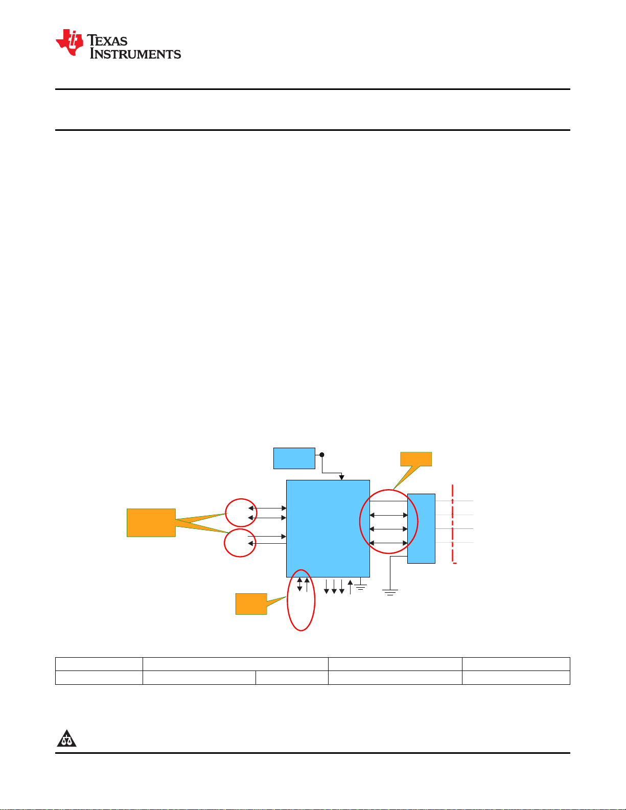
TYPICAL APPLICATION DIAGRAM
T
A
–40°C to 85°C uQFN 0.4-mm pitch – RSV Tape and Reel TSU6111ARSVR ZTN
(1) For the most current package and ordering information, see the Package Option Addendum at the end of this document, or see the TI
Web site at www.ti.com.
(2) Package drawings, thermal data, and symbolization are available at www.ti.com/packaging.
1
PACKAGE
ORDERING INFORMATION
Please be aware that an important notice concerning availability, standard warranty, and use in critical applications of
Texas Instruments semiconductor products and disclaimers thereto appears at the end of this data sheet.
PRODUCTION DATA information is current as of publication date.
Products conform to specifications per the terms of the Texas
Instruments standard warranty. Production processing does not
necessarily include testing of all parameters.
(2)
(1)
ORDERABLE PART NUMBER TOP-SIDE MARKING
Copyright © 2012, Texas Instruments Incorporated
UART
USB
Micro
USB
DP_HT
TxD
RxD
TSU6111 SWITCH
MATRIX
DM_HT VBUS
DM_CON
DP_CON
ID_CON
Charger
Detection
Sources
And
Comp’s
Accessory
ID
Detection
ADC
I2C Interface
&
Hardware
Control
VBUS
DP
DM
ID
Buffers and/or
Comparators
JIG
INTB
SDA
SCL
VDDIO
BOOT
I2C
Interface
Switches
RxD
TxD
USB_DM
USB_DP
State Machine
Switch
Ctrl
TSU6111A
SCDS331A –FEBRUARY 2012–REVISED AUGUST 2012
www.ti.com
DESCRIPTION
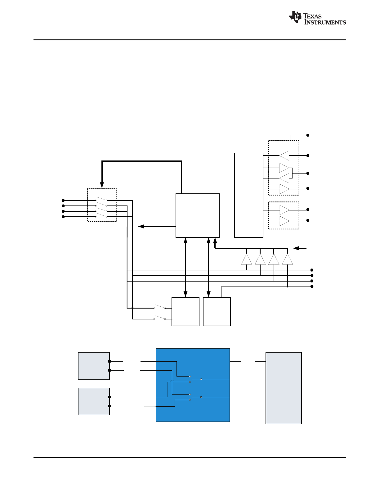
The TSU6111A is a high performance differential autonomous SP2T switch with impedance detection. The
switch supports the detection of various accessories that are attached through DP, DM, and ID. The charger
detection satisfies USB charger specification v1.1 and V
external protection. Power for this device is supplied through VBAT of the system or through V
attached to a charger.
The SP2T switch is controlled by the automatic detection logic or through manual configuration of the I2C. JIG
and BOOT pins are used when a USB or UART JIG cable is used to test the device in the development and
manufacturing. TSU6111A has open-drain JIG output (active low).
BLOCK DIAGRAM
has a 28V tolerance to eliminate the need for
BUS_IN
BUS_IN
when
SWITCH MATRIX
2 Submit Documentation Feedback Copyright © 2012, Texas Instruments Incorporated
Product Folder Link(s): TSU6111A
ID_CON
DP_CON
DM_CON
V
BUS_IN
16 15 14 13
DM_HOST 1 12 GND
DP_HOST 2 11 SDA
TxD 3 10 SCL
RxD 4 9 INTB
5 6 7 8
V
BAT
BOOT
JIG
V
DDIO
TSU6111A
www.ti.com
SCDS331A –FEBRUARY 2012–REVISED AUGUST 2012
These devices have limited built-in ESD protection. The leads should be shorted together or the device placed in conductive foam
during storage or handling to prevent electrostatic damage to the MOS gates.
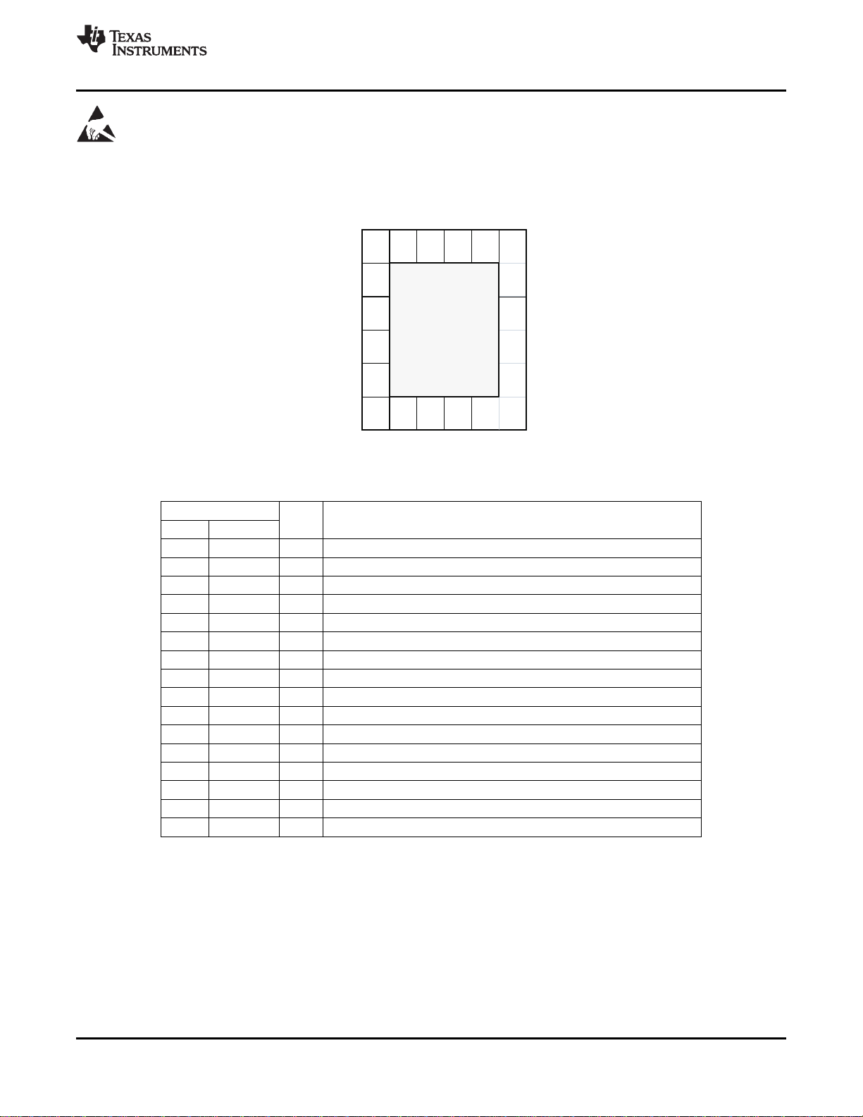
PINOUT DIAGRAM (TOP VIEW)
PIN FUNCTIONS
PIN
NO. NAME
1 DM_HOST I/O USB DM connected to host
2 DP_HOST I/O USB DP connected to host
3 TxD I/O UART Tx
4 RxD I/O UART Rx
5 VBAT I Connected to battery
6 BOOT O BOOT mode out (push-pull). Used for factory test modes.
7 JIG O JIG detection JIG detection (Open-drain). Used for factory test modes
8 VDDIO O I/O voltage reference
9 INTB O Interrupt to host (push-pull)
10 SCL I I2C clock
11 SDA I/O I2C data
12 GND Ground
13 VBUS_IN I VBUS connected to USB receptacle
14 DM_CON I/O USB DM connected to USB receptacle
15 DP_CON I/O USB DP connected to USB receptacle
16 ID_CON I/O USB ID connected to USB receptacle
I/O DESCRIPTION
Copyright © 2012, Texas Instruments Incorporated Submit Documentation Feedback 3
Product Folder Link(s): TSU6111A
TSU6111A
SCDS331A –FEBRUARY 2012–REVISED AUGUST 2012
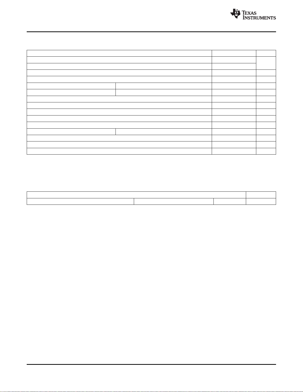
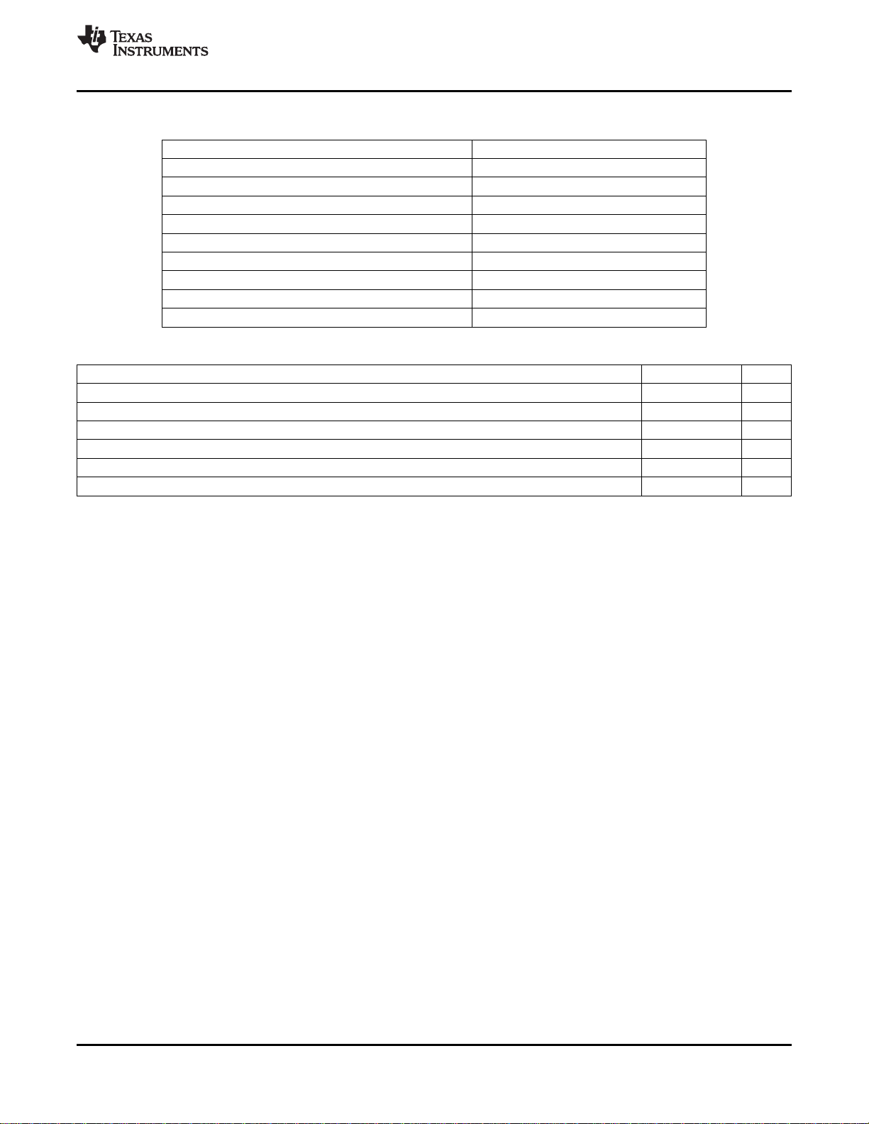
ABSOLUTE MAXIMUM RATINGS
(1)(2)
www.ti.com
over operating free-air temperature range (unless otherwise noted)
MIN MAX UNIT
V
BUS
V
BAT
V
DDIO
V
ID_CON
V
USBIO
V
UARTIO
V
JIG
V
LOGIC_O
I
K
I
SW-DC
I
SW
I
IK
I
LOGIC_O
I
GND
T
stg
(1) Stresses above these ratings may cause permanent damage. Exposure to absolute maximum conditions for extended periods may
degrade device reliability. These are stress ratings only, and functional operation of the device at these or any other conditions beyond
those specified is not implied.
(2) The algebraic convention, whereby the most negative value is a minimum and the most positive value is a maximum.
Supply voltage from USB connector –0.5 28
Supply voltage from battery –0.5 6.0
Logic supply voltage –0.5 4.6 V
ID Connector voltage –0.5 V
Switch I/O voltage range USB Switch –0.5 V
Switch I/O voltage range UART Switch –0.5 V
JIG voltage –0.5 V
+0.5 V
BAT
+0.5 V
BAT
+0.5 V
BAT
+0.5 V
BAT
Voltage applied to logic output (SCL, SDA, INTB, BOOT) –0.5 4.6 V
Analog port diode current –50 50 mA
ON-state continuous switch current –60 60 mA
ON-state peak switch current PEAK –150 150 mA
Digital logic input clamp current V
< 0 –50 mA
DDIO
Continuous current through logic output (SCL, SDA, INTB, BOOT) –50 50 mA
Continuous current through GND 100 mA
Storage temperature range –65 150 °C
V
THERMAL IMPEDANCE RATINGS
θJA Package thermal impedance RSV package 184 °C/W
UNIT
4 Submit Documentation Feedback Copyright © 2012, Texas Instruments Incorporated
Product Folder Link(s): TSU6111A
TSU6111A
www.ti.com
SCDS331A –FEBRUARY 2012–REVISED AUGUST 2012
SUMMARY OF TYPICAL CHARACTERISTICS
AMBIENT TEMPERATURE = 25°C USB/UART PATH
Number of channels 2
ON-state resistance (ron) 8 Ω
ON-state resistance match (Δron) 0.5 Ω
ON-state resistance flatness (r
Turn-on/turn-off time (tON/t
OFF
) 0.5 Ω
on(flat)
) 95 µs/ 3.5 µs
Bandwidth (BW) 920 MHz
OFF isolation (O
Crosstalk (X
Leakage current (I
) –26 dB at 250 MHz
ISO
) –32 dB at 250 MHz
TALK
) 50 nA
IO(ON)
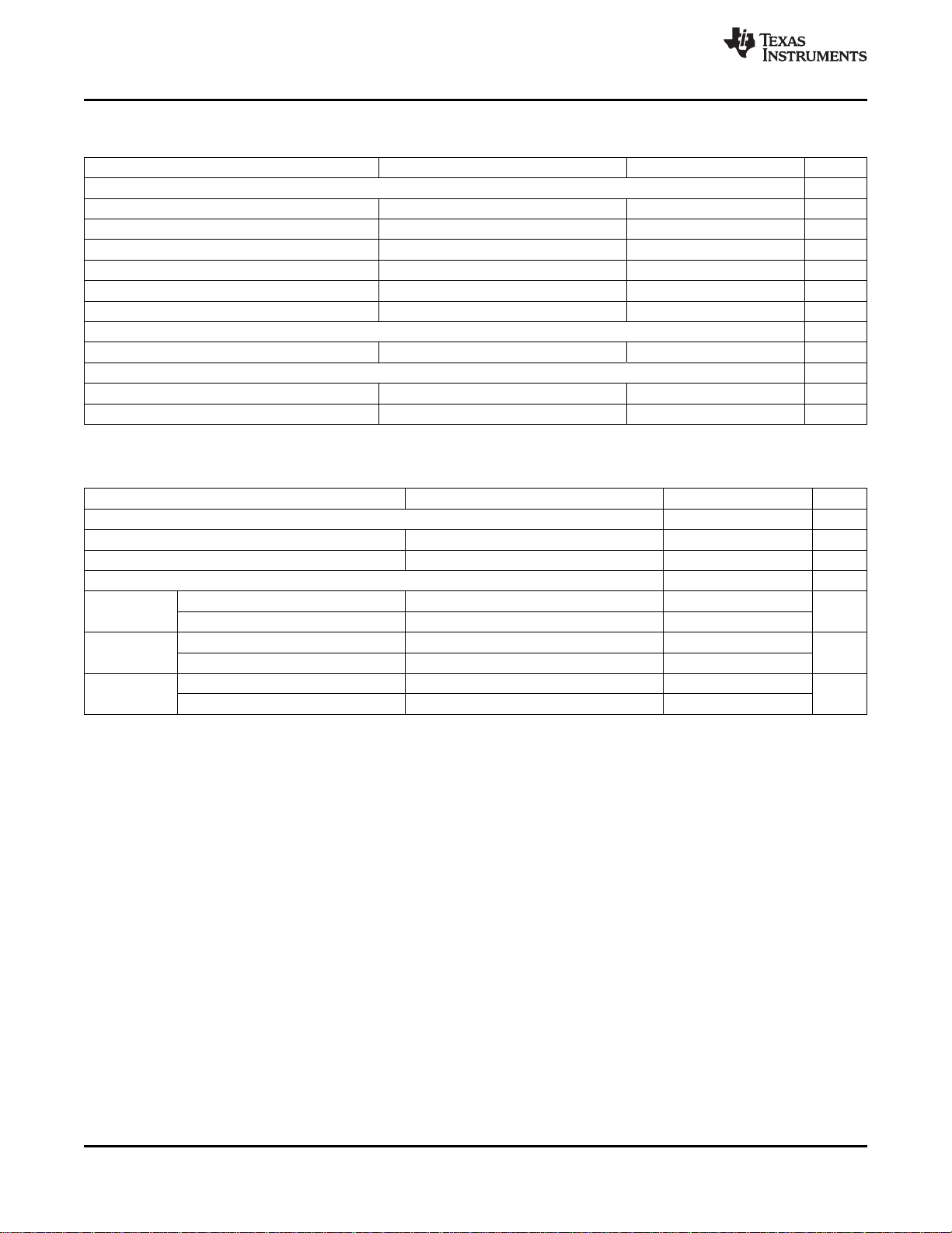
RECOMMENDED OPERATING CONDITIONS
MIN MAX UNIT
V
BUS_IN
V
BAT
V
DDIO
ID_CON_Cap ID_CON capacitance 1 nF
USB_I/O USB path signal range 0 3.6 V
Temperature Operating Temperature –40 85 °C
VBUS voltage 4.0 6.5 V
VBAT voltage 3.0 4.4 V
VDDIO voltage 1.65 3.6 V
Copyright © 2012, Texas Instruments Incorporated Submit Documentation Feedback 5
Product Folder Link(s): TSU6111A
TSU6111A
SCDS331A –FEBRUARY 2012–REVISED AUGUST 2012
www.ti.com
ELECTRICAL SPECIFICATION
over operating free-air temperature range (unless otherwise noted)
PARAMETERS TEST CONDITIONS MIN MAX UNIT
DIGITAL SIGNALS – I2C INTERFACE (SCL and SDA)
V
DDIO
V
IH
V
IL
V
OH
V
OL
f
SCL
JIG OUTPUT (TSU6111A – OPEN-DRAIN OUTPUT, ACTIVE LOW)
V
OL
INTB AND BOOT (PUSH-PULL OUTPUT)
V
OH
V
OL
ELECTRICAL SPECIFICATIONS
over operating free-air temperature range (unless otherwise noted)
TOTAL SWITCH CURRENT CONSUMPTION
I
BAT(Standby)
I
DD(Operating)
VOLTAGE PROTECTION
V
VBUS_UVLO
V
VBAT_UVLO
V
VDDIO_UVLO
(1) VOis equal to the asserted voltage on DP_CON and DM_CON pins. VIis equal to the asserted voltage on DP_HT and DM_HT pins. I
is equal to the current on the DP_CON and DM_CON pins. IIis equal to the current on the DP_HT and DM_HT pins.
Logic and I/O supply voltage 1.65 3.6 V
High-level input voltage V
Low-level input voltage 0 V
High-level output voltage IOH= –3 mA V
× 0.7 V
DDIO
× 0.3 V
DDIO
× 0.7 V
DDIO
DDIO
V
Low-level output voltage IOL= 3 mA 0.4 V
SCL frequency 400 kHz
Low-level output voltage IOL= 10 mA, V
High-level output voltage IOH= –4 mA , V
Low-level output voltage IOL= 4 mA , V
(1)
= 3.0 V 0.5 V
BAT
= 1.65 V 1.16 V
DDIO
= 1.65 V 0 0.33 V
DDIO
DDIO
V
PARAMETER TEST CONDITIONS MIN TYP MAX UNIT
V
Standby current consumption V
BAT
V
Operating current consumption V
BAT
V
under voltage + Voltage is rising 2.85
BUS
V
under voltage– Voltage is falling 2.55
BUS
V
under voltage + Voltage is rising 2.65
BUS
V
under voltage– Voltage is falling 2.45
BUS
V
under voltage + Voltage is rising 1.30
BUS
V
under voltage– Voltage is falling 1.05
BUS
= 0 V, Idle state 25 30 µA
BUS
= 0 V, USB switches ON 45 75 µA
BUS_IN
V
V
V
O
6 Submit Documentation Feedback Copyright © 2012, Texas Instruments Incorporated
Product Folder Link(s): TSU6111A

TSU6111A
www.ti.com
USB AND UART SWITCH ELECTRICAL CHARACTERISTICS
SCDS331A –FEBRUARY 2012–REVISED AUGUST 2012
(1)
over operating free-air temperature range (unless otherwise noted)
PARAMETER TEST CONDITIONS MIN TYP MAX UNIT
ANALOG SWITCH
V
r
ON
Δr
r
ON(flat)
I
IO(OFF)VI
I
IO(ON)VO
DYNAMIC
t
ON
t
OFF
C
C
C
C
BW Bandwidth RL= 50 Ω, Switch ON 920 MHz
O
X
Analog signal range 0 V
USBIO
ON-state resistance 8 15 Ω
ON-state resistance DM_HT, DP_HT,
ON
match between channels DM_CON, DP_CON
ON-state resistance
flatness
DM_HT, DP_HT, VI= 0 V to 3.6 V, IO= –2 mA,
DM_CON, DP_CON V
= 3.0 V
BAT
VI= 0.4 V, IO= –2 mA, V
BAT
DM_HT, DP_HT, VI= 0 V to 3.6 V, IO= –2 mA,
DM_CON, DP_CON V
BAT
= 3.0 V
= 3.0 V 0.5 2 Ω
VI= 0.3 V, VO= 2.7 V or
or VOOFF leakage current VI= 2.7 V, VO= 0.3 V, 45 200 nA
V
= 4.4 V, Switch OFF
BAT
ON leakage current 50 200 nA
Turn-ON time VIor VO= V
Turn-OFF time VIor VO= V
I(OFF)VI
O(OFF)VO
I(ON)
O(ON)
ISO
TALK
OFF capacitance 4 pF
OFF capacitance 7 pF
, DC bias = 0 V or 3.6 V, f = 10 MHz,
VI, VOON capacitance 9 pF
OFF Isolation f = 240 MHz, RL= 50 Ω, Switch OFF –26 dB
Crosstalk f = 240 MHz, RL= 50 Ω –32 dB
From receipt of I2C ACK
bit
From receipt of I2C ACK
bit
VI= OPEN, VO= 0.3 V or 2.7 V,
V
= 4.4 V, Switch ON
BAT
, RL= 50 Ω, CL= 35 pF 95 µs
BAT
, RL= 50 Ω, CL= 35 pF 3.5 µs
BAT
DC bias = 0 V or 3.6 V, f = 10 MHz,
Switch OFF
DC bias = 0 V or 3.6 V, f = 10 MHz,
Switch OFF
Switch ON
BAT
0.5 2 Ω
V
(1) VOis equal to the asserted voltage on DP_CON and DM_CON pins. VIis equal to the asserted voltage on DP_HT and DM_HT pins. I
is equal to the current on the DP_CON and DM_CON pins. IIis equal to the current on the DP_HT and DM_HT pins.
O
Copyright © 2012, Texas Instruments Incorporated Submit Documentation Feedback 7
Product Folder Link(s): TSU6111A

TSU6111A
SCDS331A –FEBRUARY 2012–REVISED AUGUST 2012
www.ti.com
GENERAL OPERATION
The TSU6111A will automatically detect accessories plugged into the phone via the mini/micro USB 5 pin
connector. The type of accessory detected will be stored in I2C registers within the TSU6111A for retrieval by the
host. The TSU6111A has a network of switches that are automatically opened and closed based on the
accessory detection. See Table 1 for details of which switches are open during each mode of operation. The
TSU6111A also offers a manual switching mode that allows the host processor to decide which switches should
be opened and closed. The manual switching settings are executed through the I2C interface.
STANDBY MODE
Standby mode is the default mode upon power up and occurs when no accessory has been detected. During this
mode, the VBUS and ID lines are continually monitored through comparators to determine when an accessory is
inserted. Power consumption is minimal during standby mode.
POWER SUPERVISOR
TSU6111A uses VBAT as the primary supply voltage. VBUS is the secondary supply. VDDIO is used for I2C
communication.
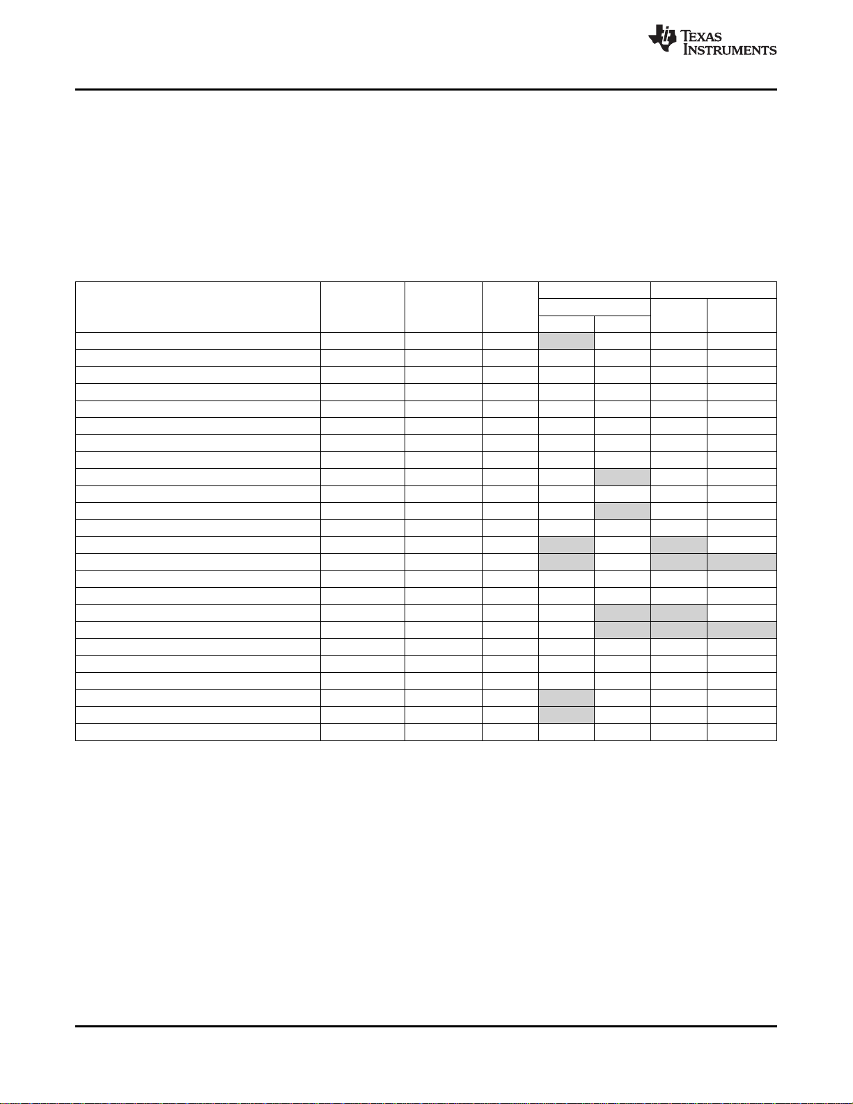
Table 1. Function Table
TSU6111A
VBAT VBUS VDDIO DETECTION I2C COMMENTS
Yes No No Enabled Not enabled VBAT is supply
Yes Yes No Enabled Not enabled VBAT is supply
Yes No Yes Enabled Enabled VBAT is supply
Yes Yes Yes Enabled Enabled VBAT is supply
No Yes No Enabled Not enabled VBUS is supply
No Yes Yes Not valid
No No Yes Not valid
No No No Power Down Reset
8 Submit Documentation Feedback Copyright © 2012, Texas Instruments Incorporated
Product Folder Link(s): TSU6111A

TSU6111A
www.ti.com
EYE DIAGRAM USB 2.0 HIGH SPEED
SCDS331A –FEBRUARY 2012–REVISED AUGUST 2012
Copyright © 2012, Texas Instruments Incorporated Submit Documentation Feedback 9
Product Folder Link(s): TSU6111A
TSU6111A
SCDS331A –FEBRUARY 2012–REVISED AUGUST 2012
www.ti.com
ACCESSORY ID DETECTION
If V
low and an accessory is attached, then use an ADC for impedance sensing on the ID pin to identify which
accessory is attached.
is high and the attachment is not a charger, then determine the impedance on the ID pin. If V
BUS_IN
BUS_IN
IMPEDANCE BUCKETS FOR EACH ACCESSORY
In order to implement ID detection, each accessory should contain a ID impedance resistor value (refer
toTable 2) which has a 5% tolerance accuracy.
Table 2. Accessory ID and Switch States
ACCCESSORY IMPEDANCE TOLERANCE DP/DM
DETECTED RESISTOR
ON ID (%)
OTG 0 — 0 ON OFF OFF OFF
MHL 1K 5% 0 OFF OFF OFF OFF
Audio Device Type 3 28.7K 5% 1110 OFF OFF OFF OFF
Reserved Accessory #1 34K 5% 1111 OFF OFF OFF OFF
Reserved Accessory #2 40.2K 5% 10000 OFF OFF OFF OFF
Reserved Accessory #3 49.9K 5% 10001 OFF OFF OFF OFF
Reserved Accessory #4 64.9K 5% 10010 OFF OFF OFF OFF
Audio Device Type 2 80.27K 5% 10011 OFF OFF OFF OFF
Phone Powered Device 102K 5% 10100 OFF ON OFF OFF
TTY Converter 121K 5% 10101 OFF OFF OFF OFF
UART Cable 150K 5% 10110 OFF ON OFF OFF
Type 1 Charger 200K 5% 10111 OFF OFF OFF OFF
Factory Mode Cable - Boot Off USB 255K 5% 11000 ON OFF ON OFF
Factory Mode Cable - Boot On USB 301K 5% 11001 ON OFF ON ON
Audio/Video Cable 365K 5% 11010 OFF OFF OFF OFF
Type 2 Charger 442K 5% 11011 OFF OFF OFF OFF
Factory Mode Cable - Boot Off UART 523K 5% 11100 OFF ON ON OFF
Factory Mode Cable - Boot On UART 619K 5% 11101 OFF ON ON ON
Stereo Headset with Remote (Audio Device Type 1) 1000.07K 10% 11110 OFF OFF OFF OFF
Mono/Stereo Headset (Audio Device Type 1) 1002K 10% 11110 OFF OFF OFF OFF
No ID — — 11111 OFF OFF OFF OFF
USB Standard Downstream Port — — 11111 ON OFF OFF OFF
USB Charging Downstream Port — — 11111 ON OFF OFF OFF
Dedicated Charging Port — — 11111 OFF OFF OFF OFF
ADC
VALUE
SWITCH STATE FACTORY CABLE
USB UART
JIG BOOT
is
10 Submit Documentation Feedback Copyright © 2012, Texas Instruments Incorporated
Product Folder Link(s): TSU6111A
TSU6111A
www.ti.com
SCDS331A –FEBRUARY 2012–REVISED AUGUST 2012
Power-On Reset
When power (from 0 V) is applied to V
until V
has reached V
BAT
. Once V
POR
registers and I2C state machine initialize to their default states.
After the initial power-up phase, V
(V
) for a power-reset cycle.
DDIO
BAT
, an internal power-on reset holds the TSU6111A in a reset condition
BAT
has reached V
BAT
, the reset condition is released, and the TSU6111A
POR
must be lowered to below 0.2 V and then back up to the operating voltage
Software Reset
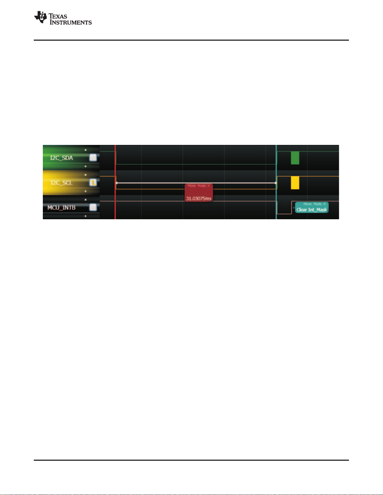
The TSU6111A has software reset feature.
• Hold low both I2C_SCL and I2C_SDA for more than 30ms to reset digital logic of the TSU6111A.
After resetting the digital logic, INTB will keep low until INT_Mask bit of Control register (0x02) is cleared.
Figure 1. Software Reset
Copyright © 2012, Texas Instruments Incorporated Submit Documentation Feedback 11
Product Folder Link(s): TSU6111A
 Loading...