

Page 1

l
! "##$$
%# ! #&'( ) #&'(
Data Manua
April 2004 MSDS 1394
SLLS512E
Page 2

IMPORTANT NOTICE
Texas Instruments Incorporated and its subsidiaries (TI) reserve the right to make corrections, modifications,
enhancements, improvements, and other changes to its products and services at any time and to discontinue
any product or service without notice. Customers should obtain the latest relevant information before placing
orders and should verify that such information is current and complete. All products are sold subject to TI’s terms
and conditions of sale supplied at the time of order acknowledgment.
TI warrants performance of its hardware products to the specifications applicable at the time of sale in
accordance with TI’s standard warranty. Testing and other quality control techniques are used to the extent TI
deems necessary to support this warranty . Except where mandated by government requirements, testing of all
parameters of each product is not necessarily performed.
TI assumes no liability for applications assistance or customer product design. Customers are responsible for
their products and applications using TI components. To minimize the risks associated with customer products
and applications, customers should provide adequate design and operating safeguards.
TI does not warrant or represent that any license, either express or implied, is granted under any TI patent right,
copyright, mask work right, or other TI intellectual property right relating to any combination, machine, or process
in which TI products or services are used. Information published by TI regarding third-party products or services
does not constitute a license from TI to use such products or services or a warranty or endorsement thereof.
Use of such information may require a license from a third party under the patents or other intellectual property
of the third party, or a license from TI under the patents or other intellectual property of TI.
Reproduction of information in TI data books or data sheets is permissible only if reproduction is without
alteration and is accompanied by all associated warranties, conditions, limitations, and notices. Reproduction
of this information with alteration is an unfair and deceptive business practice. TI is not responsible or liable for
such altered documentation.
Resale of TI products or services with statements different from or beyond the parameters stated by TI for that
product or service voids all express and any implied warranties for the associated TI product or service and is
an unfair and deceptive business practice. TI is not responsible or liable for any such statements.
Following are URLs where you can obtain information on other Texas Instruments products and application
solutions:
Products Applications
Amplifiers amplifier.ti.com Audio www.ti.com/audio
Data Converters dataconverter.ti.com Automotive www.ti.com/automotive
DSP dsp.ti.com Broadband www.ti.com/broadband
Interface interface.ti.com Digital Control www.ti.com/digitalcontrol
Logic logic.ti.com Military www.ti.com/military
Power Mgmt power.ti.com Optical Networking www.ti.com/opticalnetwork
Microcontrollers microcontroller.ti.com Security www.ti.com/security
Telephony www.ti.com/telephony
Video & Imaging www.ti.com/video
Wireless www.ti.com/wireless
Mailing Address: Texas Instruments
Post Office Box 655303, Dallas, Texas 75265
Copyright 2004, Texas Instruments Incorporated
Page 3

Contents
Section Title Page
1 Introduction 1−1. . . . . . . . . . . . . . . . . . . . . . . . . . . . . . . . . . . . . . . . . . . . . . . . . . . . . .
1.1 Features 1−1. . . . . . . . . . . . . . . . . . . . . . . . . . . . . . . . . . . . . . . . . . . . . . . . . . .
1.2 Description 1−2. . . . . . . . . . . . . . . . . . . . . . . . . . . . . . . . . . . . . . . . . . . . . . . . .
1.3 Terminal Assignments 1−3. . . . . . . . . . . . . . . . . . . . . . . . . . . . . . . . . . . . . . . .
1.4 Terminal Functions 1−4. . . . . . . . . . . . . . . . . . . . . . . . . . . . . . . . . . . . . . . . . .
1.4.1 DMA/Bulky Data Interface 1−4. . . . . . . . . . . . . . . . . . . . . . . . . . .
1.4.2 Microcontroller/Microprocessor Signals 1−5. . . . . . . . . . . . . . . .
1.4.3 Physical Layer 1−5. . . . . . . . . . . . . . . . . . . . . . . . . . . . . . . . . . . . .
1.4.4 Test Interface 1−6. . . . . . . . . . . . . . . . . . . . . . . . . . . . . . . . . . . . . .
1.4.5 Power Supplies 1−7. . . . . . . . . . . . . . . . . . . . . . . . . . . . . . . . . . . . .
1.4.6 Miscellaneous 1−7. . . . . . . . . . . . . . . . . . . . . . . . . . . . . . . . . . . . . .
1.5 Terminal Assignments for TSB43AA82A 1−8. . . . . . . . . . . . . . . . . . . . . . . .
1.5.1 144-Terminal PGE Package 1−8. . . . . . . . . . . . . . . . . . . . . . . . . .
1.5.2 176-Terminal GGW Package 1−9. . . . . . . . . . . . . . . . . . . . . . . . .
2 Architecture 2−1. . . . . . . . . . . . . . . . . . . . . . . . . . . . . . . . . . . . . . . . . . . . . . . . . . . . . .
2.1 Host I/F 2−2. . . . . . . . . . . . . . . . . . . . . . . . . . . . . . . . . . . . . . . . . . . . . . . . . . . .
2.2 DMA I/F (Bulky Data I/F) 2−2. . . . . . . . . . . . . . . . . . . . . . . . . . . . . . . . . . . . .
2.3 Configuration Register (CFR) 2−2. . . . . . . . . . . . . . . . . . . . . . . . . . . . . . . . .
2.4 Fast ORB Exchanger (FOX) 2−2. . . . . . . . . . . . . . . . . . . . . . . . . . . . . . . . . .
2.5 Auto Response (AR) 2−2. . . . . . . . . . . . . . . . . . . . . . . . . . . . . . . . . . . . . . . . .
2.6 Transaction/Timer Manager (TrMgr) 2−2. . . . . . . . . . . . . . . . . . . . . . . . . . . .
2.7 Packet Distributor 2−3. . . . . . . . . . . . . . . . . . . . . . . . . . . . . . . . . . . . . . . . . . .
2.8 Packetizer 2−3. . . . . . . . . . . . . . . . . . . . . . . . . . . . . . . . . . . . . . . . . . . . . . . . . .
2.9 Configuration ROM 2−3. . . . . . . . . . . . . . . . . . . . . . . . . . . . . . . . . . . . . . . . . .
2.10 Link Core 2−3. . . . . . . . . . . . . . . . . . . . . . . . . . . . . . . . . . . . . . . . . . . . . . . . . . .
2.11 PHY (and PHY Interface) 2−3. . . . . . . . . . . . . . . . . . . . . . . . . . . . . . . . . . . . .
2.12 FIFOs 2−3. . . . . . . . . . . . . . . . . . . . . . . . . . . . . . . . . . . . . . . . . . . . . . . . . . . . . .
2.13 Example System Block Diagrams 2−4. . . . . . . . . . . . . . . . . . . . . . . . . . . . . .
2.13.1 Asynchronous Mode With Separate Microcontroller
and DMA Bus 2−4. . . . . . . . . . . . . . . . . . . . . . . . . . . . . . . . . . . . . .
2.13.2 SCSI Mode With Shared Microcontroller and DMA Bus 2−5. .
3 Configuration Register (CFR) 3−1. . . . . . . . . . . . . . . . . . . . . . . . . . . . . . . . . . . . . .
3.1 Addressing 3−1. . . . . . . . . . . . . . . . . . . . . . . . . . . . . . . . . . . . . . . . . . . . . . . . .
3.2 Data Bit/Byte Order 3−1. . . . . . . . . . . . . . . . . . . . . . . . . . . . . . . . . . . . . . . . . .
3.3 Write/Read Access 3−6. . . . . . . . . . . . . . . . . . . . . . . . . . . . . . . . . . . . . . . . . .
3.4 CFR Definitions 3−6. . . . . . . . . . . . . . . . . . . . . . . . . . . . . . . . . . . . . . . . . . . . .
3.4.1 Version/Revision Register at 00h 3−6. . . . . . . . . . . . . . . . . . . . .
iii
Page 4

3.4.2 Miscellaneous Register at 04h 3−7. . . . . . . . . . . . . . . . . . . . . . . .
3.4.3 Control Register at 08h 3−7. . . . . . . . . . . . . . . . . . . . . . . . . . . . . .
3.4.4 Interrupt/Interrupt Mask Registers at 0Ch/10h 3−9. . . . . . . . . .
3.4.5 Cycle Timer Register at 14h 3−10. . . . . . . . . . . . . . . . . . . . . . . . . .
3.4.6 Diagnostics Register at 18h 3−10. . . . . . . . . . . . . . . . . . . . . . . . . .
3.4.7 Reserved at 1Ch 3−11. . . . . . . . . . . . . . . . . . . . . . . . . . . . . . . . . . .
3.4.8 PHY Access Register at 20h 3−11. . . . . . . . . . . . . . . . . . . . . . . . .
3.4.9 Bus Reset Register at 24h 3−11. . . . . . . . . . . . . . . . . . . . . . . . . . .
3.4.10 Time Limit Register at 28h 3−12. . . . . . . . . . . . . . . . . . . . . . . . . . .
3.4.11 ATF Status Register at 2Ch 3−12. . . . . . . . . . . . . . . . . . . . . . . . . .
3.4.12 ARF Status Register at 30h 3−13. . . . . . . . . . . . . . . . . . . . . . . . . .
3.4.13 MTQ Status Register at 34h 3−13. . . . . . . . . . . . . . . . . . . . . . . . . .
3.4.14 MRF Status Register at 38h 3−14. . . . . . . . . . . . . . . . . . . . . . . . . .
3.4.15 CTQ Status Register at 3Ch 3−14. . . . . . . . . . . . . . . . . . . . . . . . . .
3.4.16 CRF Status Register at 40h 3−15. . . . . . . . . . . . . . . . . . . . . . . . . .
3.4.17 ORB Fetch Control Register at 44h 3−16. . . . . . . . . . . . . . . . . . .
3.4.18 Management Agent Register at 48h 3−17. . . . . . . . . . . . . . . . . . .
3.4.19 Command Agent Register at 4Ch 3−17. . . . . . . . . . . . . . . . . . . . .
3.4.20 Agent Control Register at 50h 3−17. . . . . . . . . . . . . . . . . . . . . . . .
3.4.21 ORB Pointer Register 1 at 54h 3−18. . . . . . . . . . . . . . . . . . . . . . .
3.4.22 ORB Pointer Register 2 at 58h 3−18. . . . . . . . . . . . . . . . . . . . . . .
3.4.23 Agent Status Register at 5Ch 3−19. . . . . . . . . . . . . . . . . . . . . . . . .
3.4.24 Transaction Timer Control Register at 60h 3−20. . . . . . . . . . . . .
3.4.25 Transaction Timer Status Registers at 64h, 68h, 6Ch 3−21. . . .
3.4.26 Write-First, Write-Continue, and Write-Update Registers
at 70h, 74h, 78h 3−22. . . . . . . . . . . . . . . . . . . . . . . . . . . . . . . . . . .
3.4.27 Reserved at 7Ch 3−22. . . . . . . . . . . . . . . . . . . . . . . . . . . . . . . . . . .
3.4.28 ARF, MRF, and CRF Data Read Registers
at 80h, 84h, 88h 3−22. . . . . . . . . . . . . . . . . . . . . . . . . . . . . . . . . . .
3.4.29 Configuration ROM Control Register at 8Ch 3−23. . . . . . . . . . . .
3.4.30 DMA Control Register at 90h 3−23. . . . . . . . . . . . . . . . . . . . . . . . .
3.4.31 Bulky Interface Control Register at 94h 3−25. . . . . . . . . . . . . . . .
3.4.32 DTF/DRF and DTF/DRF Page Table Size Register
at 98h 3−26. . . . . . . . . . . . . . . . . . . . . . . . . . . . . . . . . . . . . . . . . . . .
3.4.33 DTF/DRF Available Register at 9Ch 3−26. . . . . . . . . . . . . . . . . . .
3.4.34 DTF/DRF Acknowledge Register at A0h 3−26. . . . . . . . . . . . . . .
3.4.35 DTF First and Continue Register at A4h 3−27. . . . . . . . . . . . . . .
3.4.36 DTF Update Register at A8h 3−27. . . . . . . . . . . . . . . . . . . . . . . . .
3.4.37 DRF Data Read Register at ACh 3−27. . . . . . . . . . . . . . . . . . . . . .
3.4.38 DTF Control Registers at B0h, B4h, B8h, and BCh 3−27. . . . . .
3.4.39 DRF Control Registers at C0h, C4h, C8h, and CCh
(DRPktz at 90h = 0)—Direct 3−29. . . . . . . . . . . . . . . . . . . . . . . . .
3.4.40 DRF Control Registers at C0h, C4h, C8h, and CCh
(DRPktz at 90h = 1)—Packetizer 3−30. . . . . . . . . . . . . . . . . . . . .
3.4.41 DRF Header Registers at D0h, D4h, D8h, and DCh 3−31. . . . .
iv
Page 5

3.4.42 DRF Trailer Register at E0h 3−32. . . . . . . . . . . . . . . . . . . . . . . . . .
3.4.43 DTF/DRF Page Count Register at E4h 3−32. . . . . . . . . . . . . . . .
3.4.44 DTx Write Request Header Registers at E8h, ECh, F0h,
and F4h (DhdSel at 90h = 00b) 3−33. . . . . . . . . . . . . . . . . . . . . .
3.4.45 DTF Packetizer Status Registers at E8h, ECh, F0h, and
F4h (DhdSel at 90h = 01b) 3−34. . . . . . . . . . . . . . . . . . . . . . . . . .
3.4.46 DRx Read Request Header Registers at E8h, ECh, F0h,
and F4h (DhdSel at 90h = 10b) 3−35. . . . . . . . . . . . . . . . . . . . . .
3.4.47 DRx Packetizer Status Registers at E8h, ECh, F0h, and
F4h (DhdSel at 90h = 11b) 3−36. . . . . . . . . . . . . . . . . . . . . . . . . .
3.4.48 Log/ROM Control Register at F8h 3−38. . . . . . . . . . . . . . . . . . . . .
3.4.49 Log ROM Data Register at FCh 3−39. . . . . . . . . . . . . . . . . . . . . . .
4 Asynchronous Command FIFOs 4−1. . . . . . . . . . . . . . . . . . . . . . . . . . . . . . . . . . .
4.1 Sizes of Asynchronous Command FIFOs (total 378 quadlets) 4−1. . . . .
4.1.1 MTQ/MRF 4−1. . . . . . . . . . . . . . . . . . . . . . . . . . . . . . . . . . . . . . . . .
4.1.2 CTQ/CRF 4−1. . . . . . . . . . . . . . . . . . . . . . . . . . . . . . . . . . . . . . . . . .
4.1.3 ATF/ARF 4−1. . . . . . . . . . . . . . . . . . . . . . . . . . . . . . . . . . . . . . . . . .
4.2 Asynchronous Command Transmit and Receive Data Formats 4−2. . . .
4.2.1 tLabel/tCode Management for Packet Transmission 4−2. . . . .
4.2.2 Reserved tLabel 4−2. . . . . . . . . . . . . . . . . . . . . . . . . . . . . . . . . . . .
4.2.3 Exception to the Rule 4−3. . . . . . . . . . . . . . . . . . . . . . . . . . . . . . .
4.3 Asynchronous Transmit FIFO (ATF) 4−3. . . . . . . . . . . . . . . . . . . . . . . . . . . .
4.3.1 Generic Quadlet and Block Transmit 4−3. . . . . . . . . . . . . . . . . .
4.3.2 PHY Packet Common Format 4−4. . . . . . . . . . . . . . . . . . . . . . . .
4.4 Asynchronous Receive FIFO (ARF) 4−7. . . . . . . . . . . . . . . . . . . . . . . . . . . .
4.4.1 Generic Quadlet and Block Receive 4−7. . . . . . . . . . . . . . . . . . .
4.5 Management and Command FIFOs (MTQ/CTQ and MRF/CRF) 4−9. . .
4.5.1 MTQ/CTQ Format 4−9. . . . . . . . . . . . . . . . . . . . . . . . . . . . . . . . . .
4.5.2 MRF/CRF Short Format 4−10. . . . . . . . . . . . . . . . . . . . . . . . . . . . .
4.5.3 MRF/CRF Long Format 4−10. . . . . . . . . . . . . . . . . . . . . . . . . . . . . .
5 ConfigROM and LOG FIFOs (Total 126 Quadlets) 5−1. . . . . . . . . . . . . . . . . . . .
5.1 Setting the ConfigROM and LOG FIFO Size 5−1. . . . . . . . . . . . . . . . . . . .
5.2 Configuration ROM Setup 5−1. . . . . . . . . . . . . . . . . . . . . . . . . . . . . . . . . . . .
5.3 Transaction LOG 5−2. . . . . . . . . . . . . . . . . . . . . . . . . . . . . . . . . . . . . . . . . . . .
6 Transaction Timer/Manager (TrMgr) 6−1. . . . . . . . . . . . . . . . . . . . . . . . . . . . . . . .
6.1 Confirm Transaction End 6−1. . . . . . . . . . . . . . . . . . . . . . . . . . . . . . . . . . . . .
6.2 Confirm End State 6−1. . . . . . . . . . . . . . . . . . . . . . . . . . . . . . . . . . . . . . . . . . .
6.3 Confirm Status of Ongoing Transaction 6−1. . . . . . . . . . . . . . . . . . . . . . . . .
6.4 Abort Transaction 6−2. . . . . . . . . . . . . . . . . . . . . . . . . . . . . . . . . . . . . . . . . . .
7 Fast ORB Exchanger (FOX) 7−1. . . . . . . . . . . . . . . . . . . . . . . . . . . . . . . . . . . . . . . .
7.1 Command ORB Auto-Fetch Agent 7−1. . . . . . . . . . . . . . . . . . . . . . . . . . . . .
7.1.1 Internal Agent Operation for Initiator 7−1. . . . . . . . . . . . . . . . . . .
7.1.2 Internal Agent Transaction for Write Request
From Initiator 7−2. . . . . . . . . . . . . . . . . . . . . . . . . . . . . . . . . . . . . .
7.1.3 Internal Agent Transaction for Read Request
From Initiator 7−3. . . . . . . . . . . . . . . . . . . . . . . . . . . . . . . . . . . . . .
v
Page 6

7.1.4 Controlling Command ORB Fetch Request 7−3. . . . . . . . . . . . .
7.1.5 Agent Behavior to DOORBELL Register Write 7−3. . . . . . . . . .
7.2 Management Transactions 7−3. . . . . . . . . . . . . . . . . . . . . . . . . . . . . . . . . . . .
7.2.1 Typical ORB Management ORB Fetch
Command Operation 7−4. . . . . . . . . . . . . . . . . . . . . . . . . . . . . . .
7.2.2 Login 7−4. . . . . . . . . . . . . . . . . . . . . . . . . . . . . . . . . . . . . . . . . . . . . .
7.2.3 Logout 7−6. . . . . . . . . . . . . . . . . . . . . . . . . . . . . . . . . . . . . . . . . . . .
7.3 SBP-2 Linked Command ORBs 7−7. . . . . . . . . . . . . . . . . . . . . . . . . . . . . . .
7.3.1 Typical Command ORB Fetch Command Operation 7−7. . . . .
7.3.2 SBP-2/Linked Command ORB Procedure 7−7. . . . . . . . . . . . . .
8 BD FIFOs (Total 1182 Quadlets) 8−1. . . . . . . . . . . . . . . . . . . . . . . . . . . . . . . . . . . .
8.1 Setting the BD FIFO Size 8−1. . . . . . . . . . . . . . . . . . . . . . . . . . . . . . . . . . . . .
8.1.1 DTF 8−1. . . . . . . . . . . . . . . . . . . . . . . . . . . . . . . . . . . . . . . . . . . . . . .
8.1.2 DRF 8−1. . . . . . . . . . . . . . . . . . . . . . . . . . . . . . . . . . . . . . . . . . . . . .
8.2 DTF/DRF Packet Format 8−1. . . . . . . . . . . . . . . . . . . . . . . . . . . . . . . . . . . . .
8.2.1 DRF Packet Format 8−1. . . . . . . . . . . . . . . . . . . . . . . . . . . . . . . . .
8.2.2 DTF Packet Format 8−2. . . . . . . . . . . . . . . . . . . . . . . . . . . . . . . . .
8.3 Status Block Setup 8−3. . . . . . . . . . . . . . . . . . . . . . . . . . . . . . . . . . . . . . . . . .
8.4 DMA Operation 8−4. . . . . . . . . . . . . . . . . . . . . . . . . . . . . . . . . . . . . . . . . . . . .
8.4.1 Packet Transmission by DTF 8−4. . . . . . . . . . . . . . . . . . . . . . . . .
8.4.2 Packet Receipt With DRF 8−6. . . . . . . . . . . . . . . . . . . . . . . . . . . .
8.4.3 Reading DRF Through the CFR 8−7. . . . . . . . . . . . . . . . . . . . . .
8.4.4 Reading DRF Through the Bulky Interface 8−8. . . . . . . . . . . . .
9 DMA Interface 9−1. . . . . . . . . . . . . . . . . . . . . . . . . . . . . . . . . . . . . . . . . . . . . . . . . . . .
9.1 Mode Setting 9−1. . . . . . . . . . . . . . . . . . . . . . . . . . . . . . . . . . . . . . . . . . . . . . .
9.1.1 Setting Active Signal 9−2. . . . . . . . . . . . . . . . . . . . . . . . . . . . . . . .
9.2 Synchronous Mode (Modes A, D, and G) 9−2. . . . . . . . . . . . . . . . . . . . . . .
9.2.1 Request Transmission (Memory → TSB43AA82A)
(Modes A, D, and G) 9−2. . . . . . . . . . . . . . . . . . . . . . . . . . . . . . . .
9.2.2 Receiving Transmission (TSB43AA82A → Memory)
(Modes A, D, and G) 9−3. . . . . . . . . . . . . . . . . . . . . . . . . . . . . . . .
9.2.3 Timing Values (Modes A, D, and G) 9−4. . . . . . . . . . . . . . . . . . .
9.3 Asynchronous SCSI Mode (Modes E and H) 9−5. . . . . . . . . . . . . . . . . . . .
9.3.1 Request Transmission (Memory → TSB43AA82A)
(Modes E and H) 9−5. . . . . . . . . . . . . . . . . . . . . . . . . . . . . . . . . . .
9.3.2 Receiving Transmission (TSB43AA82A → Memory)
(Modes E and H) 9−5. . . . . . . . . . . . . . . . . . . . . . . . . . . . . . . . . . .
9.3.3 Timing Values (Modes E and H) 9−6. . . . . . . . . . . . . . . . . . . . . .
9.4 Asynchronous Handshake Mode (Modes B, C, and F) 9−11. . . . . . . . . . . .
9.4.1 Request Transmission (Memory → TSB43AA82A)
(Modes B, C, and F) 9−11. . . . . . . . . . . . . . . . . . . . . . . . . . . . . . . .
9.4.2 Receiving Transmission (TSB43AA82A → Memory)
(Modes B, C, and F) 9−11. . . . . . . . . . . . . . . . . . . . . . . . . . . . . . . .
9.4.3 Timing Values (Modes B, C, and F) 9−11. . . . . . . . . . . . . . . . . . .
9.5 ATAPI Mode (Mode G and Burst = 1) 9−14. . . . . . . . . . . . . . . . . . . . . . . . . . .
vi
Page 7

9.6 Endianness 9−16. . . . . . . . . . . . . . . . . . . . . . . . . . . . . . . . . . . . . . . . . . . . . . . . .
9.7 Clearing the DMA Interface Data 9−17. . . . . . . . . . . . . . . . . . . . . . . . . . . . . .
9.8 Resetting the DMA Interface 9−17. . . . . . . . . . . . . . . . . . . . . . . . . . . . . . . . . .
9.9 Suspending the BDIO Output 9−17. . . . . . . . . . . . . . . . . . . . . . . . . . . . . . . . .
10 Host Interface 10−1. . . . . . . . . . . . . . . . . . . . . . . . . . . . . . . . . . . . . . . . . . . . . . . . . . .
10.1 Parallel Mode Specification 10−1. . . . . . . . . . . . . . . . . . . . . . . . . . . . . . . . . . .
10.2 Multiplex Mode Specification 10−3. . . . . . . . . . . . . . . . . . . . . . . . . . . . . . . . . .
11 PHY 11−1. . . . . . . . . . . . . . . . . . . . . . . . . . . . . . . . . . . . . . . . . . . . . . . . . . . . . . . . . . . . .
11.1 Description 11−1. . . . . . . . . . . . . . . . . . . . . . . . . . . . . . . . . . . . . . . . . . . . . . . . .
11.2 PHY Internal Registers 11−2. . . . . . . . . . . . . . . . . . . . . . . . . . . . . . . . . . . . . . .
11.3 Power-Class Programming 11−7. . . . . . . . . . . . . . . . . . . . . . . . . . . . . . . . . . .
12 Application Information 12−1. . . . . . . . . . . . . . . . . . . . . . . . . . . . . . . . . . . . . . . . . . .
12.1 PHY Port Cable Connection 12−1. . . . . . . . . . . . . . . . . . . . . . . . . . . . . . . . . .
12.2 Crystal Selection 12−2. . . . . . . . . . . . . . . . . . . . . . . . . . . . . . . . . . . . . . . . . . . .
12.3 Bus Reset 12−3. . . . . . . . . . . . . . . . . . . . . . . . . . . . . . . . . . . . . . . . . . . . . . . . . .
12.4 Low-Power Mode 12−4. . . . . . . . . . . . . . . . . . . . . . . . . . . . . . . . . . . . . . . . . . . .
12.5 Power Down and Initialization 12−4. . . . . . . . . . . . . . . . . . . . . . . . . . . . . . . . .
12.6 Power-Supply Sequence 12−5. . . . . . . . . . . . . . . . . . . . . . . . . . . . . . . . . . . . .
13 Packet Processing With CSR Addressing 13−1. . . . . . . . . . . . . . . . . . . . . . . . . .
13.1 Ack and Response Packet for Request Packet—CFR ErrResp and
StErPkt at 08h 13−1. . . . . . . . . . . . . . . . . . . . . . . . . . . . . . . . . . . . . . . . . . . . . .
13.1.1 RAM ROM 13−1. . . . . . . . . . . . . . . . . . . . . . . . . . . . . . . . . . . . . . . . .
13.1.2 ARF ROM 13−1. . . . . . . . . . . . . . . . . . . . . . . . . . . . . . . . . . . . . . . . .
13.1.3 Outside of Configuration ROM 13−2. . . . . . . . . . . . . . . . . . . . . . . .
13.1.4 Other 13−2. . . . . . . . . . . . . . . . . . . . . . . . . . . . . . . . . . . . . . . . . . . . .
14 Electrical Characteristics 14−1. . . . . . . . . . . . . . . . . . . . . . . . . . . . . . . . . . . . . . . . .
14.1 Absolute Maximum Ratings Over Free-Air Temperature Range 14−1. . . .
14.2 Recommended Operating Conditions 14−1. . . . . . . . . . . . . . . . . . . . . . . . . .
14.3 Electrical Characteristics Over Recommended Ranges of
Operating Conditions 14−2. . . . . . . . . . . . . . . . . . . . . . . . . . . . . . . . . . . . . . . .
14.3.1 Device 14−2. . . . . . . . . . . . . . . . . . . . . . . . . . . . . . . . . . . . . . . . . . . .
14.3.2 Driver 14−3. . . . . . . . . . . . . . . . . . . . . . . . . . . . . . . . . . . . . . . . . . . . .
14.3.3 Receiver 14−3. . . . . . . . . . . . . . . . . . . . . . . . . . . . . . . . . . . . . . . . . . .
14.4 Switching Characteristics 14−3. . . . . . . . . . . . . . . . . . . . . . . . . . . . . . . . . . . . .
15 Mechanical Data 15−1. . . . . . . . . . . . . . . . . . . . . . . . . . . . . . . . . . . . . . . . . . . . . . . . .
vii
Page 8

List of Illustrations
Figure Title Page
2−1 Functional Block Architecture 2−1. . . . . . . . . . . . . . . . . . . . . . . . . . . . . . . . . . . . . . .
3−1 Automatically Creating an SBP-2 Compliant Request for a
Block Packet 3−28. . . . . . . . . . . . . . . . . . . . . . . . . . . . . . . . . . . . . . . . . . . . . . . . . . .
4−1 Generic Transmit Format of Packet With Quadlet Data 4−3. . . . . . . . . . . . . . . . .
4−2 Generic Transmit Format of Packet With Block Data 4−3. . . . . . . . . . . . . . . . . . .
4−3 PHY Packet Format 4−4. . . . . . . . . . . . . . . . . . . . . . . . . . . . . . . . . . . . . . . . . . . . . . .
4−4 Link-On Packet 4−5. . . . . . . . . . . . . . . . . . . . . . . . . . . . . . . . . . . . . . . . . . . . . . . . . . .
4−5 PING Packet 4−5. . . . . . . . . . . . . . . . . . . . . . . . . . . . . . . . . . . . . . . . . . . . . . . . . . . . .
4−6 Remote Access Packet 4−6. . . . . . . . . . . . . . . . . . . . . . . . . . . . . . . . . . . . . . . . . . . .
4−7 Remote Command Packet 4−6. . . . . . . . . . . . . . . . . . . . . . . . . . . . . . . . . . . . . . . . .
4−8 Resume Packet 4−7. . . . . . . . . . . . . . . . . . . . . . . . . . . . . . . . . . . . . . . . . . . . . . . . . . .
4−9 Generic Receive Format of Packet With Quadlet Data 4−7. . . . . . . . . . . . . . . . .
4−10 Generic Receive Format of Packet With Block Data 4−8. . . . . . . . . . . . . . . . . .
4−11 MTQ/CTQ Transmission Block Read Packet Format 4−9. . . . . . . . . . . . . . . . . .
4−12 MRF/CRF Receive Short Format (ORB) 4−10. . . . . . . . . . . . . . . . . . . . . . . . . . . .
4−13 MRF/CRF Receive Long Format (ORB) 4−10. . . . . . . . . . . . . . . . . . . . . . . . . . . . .
5−1 Example ConfigROM Base Structure (Reference SBP-2 Draft) 5−1. . . . . . . . . .
5−2 ConfigROM Setup 5−2. . . . . . . . . . . . . . . . . . . . . . . . . . . . . . . . . . . . . . . . . . . . . . . .
7−1 Command Agent Registers 7−1. . . . . . . . . . . . . . . . . . . . . . . . . . . . . . . . . . . . . . . . .
7−2 Typical Login Process 7−5. . . . . . . . . . . . . . . . . . . . . . . . . . . . . . . . . . . . . . . . . . . . .
7−3 Typical Management ORB Transaction 7−6. . . . . . . . . . . . . . . . . . . . . . . . . . . . . .
7−4 Logout Process 7−6. . . . . . . . . . . . . . . . . . . . . . . . . . . . . . . . . . . . . . . . . . . . . . . . . . .
7−5 Typical Link Fetch 7−8. . . . . . . . . . . . . . . . . . . . . . . . . . . . . . . . . . . . . . . . . . . . . . . . .
7−6 SUSPENDED and DOORBELL Request by Dummy ORB 7−9. . . . . . . . . . . . . .
7−7 UNSOLICITED_STATUS_ENABLE 7−10. . . . . . . . . . . . . . . . . . . . . . . . . . . . . . . . .
8−1 DRF Block-Receive Packet Format 8−1. . . . . . . . . . . . . . . . . . . . . . . . . . . . . . . . . .
8−2 DTF Packet Format With Block Data 8−3. . . . . . . . . . . . . . . . . . . . . . . . . . . . . . . .
8−3 Status Block Format 8−3. . . . . . . . . . . . . . . . . . . . . . . . . . . . . . . . . . . . . . . . . . . . . . .
9−1 Synchronous Mode 9−4. . . . . . . . . . . . . . . . . . . . . . . . . . . . . . . . . . . . . . . . . . . . . . .
9−2 SCSI Handshake Mode 9−6. . . . . . . . . . . . . . . . . . . . . . . . . . . . . . . . . . . . . . . . . . . .
9−3 SCSI Burst Mode Write (1) 9−7. . . . . . . . . . . . . . . . . . . . . . . . . . . . . . . . . . . . . . . . .
9−4 SCSI Burst Mode Write (2) 9−8. . . . . . . . . . . . . . . . . . . . . . . . . . . . . . . . . . . . . . . . .
9−5 SCSI Burst Mode Write (3) 9−9. . . . . . . . . . . . . . . . . . . . . . . . . . . . . . . . . . . . . . . . .
viii
Page 9

9−6 SCSI Burst Mode Write (4) 9−10. . . . . . . . . . . . . . . . . . . . . . . . . . . . . . . . . . . . . . . . .
9−7 Asynchronous Mode 9−11. . . . . . . . . . . . . . . . . . . . . . . . . . . . . . . . . . . . . . . . . . . . . .
9−8 Asynchronous Handshake Mode Write 9−12. . . . . . . . . . . . . . . . . . . . . . . . . . . . . . .
9−9 Asynchronous Handshake Mode Read 9−12. . . . . . . . . . . . . . . . . . . . . . . . . . . . . .
9−10 Asynchronous Burst Mode Write 9−13. . . . . . . . . . . . . . . . . . . . . . . . . . . . . . . . . . .
9−11 Asynchronous Burst Mode Read 9−13. . . . . . . . . . . . . . . . . . . . . . . . . . . . . . . . . . .
9−12 ATAPI Initiate (Read) 9−14. . . . . . . . . . . . . . . . . . . . . . . . . . . . . . . . . . . . . . . . . . . . .
9−13 ATAPI Read 9−14. . . . . . . . . . . . . . . . . . . . . . . . . . . . . . . . . . . . . . . . . . . . . . . . . . . . .
9−14 ATAPI Terminate (Read) 9−14. . . . . . . . . . . . . . . . . . . . . . . . . . . . . . . . . . . . . . . . . .
9−15 ATAPI Initiate (Write) 9−15. . . . . . . . . . . . . . . . . . . . . . . . . . . . . . . . . . . . . . . . . . . . .
9−16 ATAPI Write 9−15. . . . . . . . . . . . . . . . . . . . . . . . . . . . . . . . . . . . . . . . . . . . . . . . . . . . .
9−17 ATAPI Terminate (Write) 9−15. . . . . . . . . . . . . . . . . . . . . . . . . . . . . . . . . . . . . . . . . .
10−1 Parallel Mode Read/Write Cycle 10−1. . . . . . . . . . . . . . . . . . . . . . . . . . . . . . . . . . .
10−2 Multiplex (MUX) Mode Read/Write Cycle 10−3. . . . . . . . . . . . . . . . . . . . . . . . . . . .
12−1 TP Cable Connections 12−1. . . . . . . . . . . . . . . . . . . . . . . . . . . . . . . . . . . . . . . . . . . .
12−2 Nonisolated Outer Shield Termination for 6-Pin Connector 12−2. . . . . . . . . . . .
12−3 Nonisolated Outer Shield Termination for 4-Pin Connector 12−2. . . . . . . . . . . .
12−4 Load Capacitance for the TSB43AA82A PHY Portion 12−3. . . . . . . . . . . . . . . . .
12−5 Recommended Crystal and Capacitor Layout 12−3. . . . . . . . . . . . . . . . . . . . . . . .
12−6 Initialization Sequence 12−5. . . . . . . . . . . . . . . . . . . . . . . . . . . . . . . . . . . . . . . . . . . .
12−7 Power-Up Sequence 12−5. . . . . . . . . . . . . . . . . . . . . . . . . . . . . . . . . . . . . . . . . . . . .
12−8 Power-Down Sequence 12−6. . . . . . . . . . . . . . . . . . . . . . . . . . . . . . . . . . . . . . . . . . .
List of Tables
Table Title Page
2−1 Address/Data 2−2. . . . . . . . . . . . . . . . . . . . . . . . . . . . . . . . . . . . . . . . . . . . . . . . . . . . .
3−1 CFR Map 3−2. . . . . . . . . . . . . . . . . . . . . . . . . . . . . . . . . . . . . . . . . . . . . . . . . . . . . . . .
3−2 DTFCtl: DTF Packetizer Transmit Control 3−28. . . . . . . . . . . . . . . . . . . . . . . . . . . .
3−3 DRFCtl: DRF Packetizer Transmit Control 3−30. . . . . . . . . . . . . . . . . . . . . . . . . . . .
4−1 Block-Transmit Format Descriptions 4−4. . . . . . . . . . . . . . . . . . . . . . . . . . . . . . . . .
4−2 PHY Packet Format Descriptions 4−5. . . . . . . . . . . . . . . . . . . . . . . . . . . . . . . . . . .
4−3 Link-On Packet Descriptions 4−5. . . . . . . . . . . . . . . . . . . . . . . . . . . . . . . . . . . . . . .
4−4 PING Packet Descriptions 4−5. . . . . . . . . . . . . . . . . . . . . . . . . . . . . . . . . . . . . . . . . .
4−5 Remote Access Packet Descriptions 4−6. . . . . . . . . . . . . . . . . . . . . . . . . . . . . . . .
4−6 Remote Command Packet Descriptions 4−6. . . . . . . . . . . . . . . . . . . . . . . . . . . . . .
4−7 Resume Packet Descriptions 4−7. . . . . . . . . . . . . . . . . . . . . . . . . . . . . . . . . . . . . . .
4−8 Generic Receive Format Descriptions 4−8. . . . . . . . . . . . . . . . . . . . . . . . . . . . . . .
4−9 Block-Transmit Format Descriptions 4−9. . . . . . . . . . . . . . . . . . . . . . . . . . . . . . . . .
4−10 MRF/CRF Format Descriptions 4−11. . . . . . . . . . . . . . . . . . . . . . . . . . . . . . . . . . . .
ix
Page 10

6−1 FIFO/Timer and Status Bit Combinations 6−2. . . . . . . . . . . . . . . . . . . . . . . . . . . . .
7−1 Agent Transaction for Initiator Write Request 7−2. . . . . . . . . . . . . . . . . . . . . . . . .
7−2 Command Agent Response—Successful Write 7−2. . . . . . . . . . . . . . . . . . . . . . .
7−3 Command Agent Error Response 7−2. . . . . . . . . . . . . . . . . . . . . . . . . . . . . . . . . . .
7−4 Agent Transaction for Read Request From Initiator 7−3. . . . . . . . . . . . . . . . . . . .
7−5 Doorbell Special Functions 7−3. . . . . . . . . . . . . . . . . . . . . . . . . . . . . . . . . . . . . . . . .
8−1 DRF Block-Receive Format Descriptions 8−2. . . . . . . . . . . . . . . . . . . . . . . . . . . . .
8−2 Block-Transmit Format Descriptions 8−3. . . . . . . . . . . . . . . . . . . . . . . . . . . . . . . . .
8−3 Status-Block Format Descriptions 8−4. . . . . . . . . . . . . . . . . . . . . . . . . . . . . . . . . . .
9−1 Modes of the Bulky Data Interface 9−1. . . . . . . . . . . . . . . . . . . . . . . . . . . . . . . . . .
9−2 Synchronous Mode 9−4. . . . . . . . . . . . . . . . . . . . . . . . . . . . . . . . . . . . . . . . . . . . . . .
9−3 SCSI Handshake Mode 9−6. . . . . . . . . . . . . . . . . . . . . . . . . . . . . . . . . . . . . . . . . . . .
9−4 SCSI Burst Mode Write (1) 9−7. . . . . . . . . . . . . . . . . . . . . . . . . . . . . . . . . . . . . . . . .
9−5 SCSI Burst Mode Write (2) 9−8. . . . . . . . . . . . . . . . . . . . . . . . . . . . . . . . . . . . . . . . .
9−6 SCSI Burst Mode Write (3) 9−9. . . . . . . . . . . . . . . . . . . . . . . . . . . . . . . . . . . . . . . . .
9−7 SCSI Burst Mode Write (4) 9−10. . . . . . . . . . . . . . . . . . . . . . . . . . . . . . . . . . . . . . . . .
9−8 Asynchronous Mode 9−11. . . . . . . . . . . . . . . . . . . . . . . . . . . . . . . . . . . . . . . . . . . . . .
9−9 Asynchronous Handshake Mode Write and Read 9−12. . . . . . . . . . . . . . . . . . . . .
9−10 Asynchronous Burst Mode Write and Read 9−13. . . . . . . . . . . . . . . . . . . . . . . . . .
9−11 ATAPI Mode 9−16. . . . . . . . . . . . . . . . . . . . . . . . . . . . . . . . . . . . . . . . . . . . . . . . . . . . .
10−1 Parallel Mode Read/Write Cycle 10−2. . . . . . . . . . . . . . . . . . . . . . . . . . . . . . . . . . .
10−2 Multiplex Mode Read/Write Cycle 10−4. . . . . . . . . . . . . . . . . . . . . . . . . . . . . . . . . .
11−1 Base Register Configuration 11−2. . . . . . . . . . . . . . . . . . . . . . . . . . . . . . . . . . . . . . .
11−2 Base Register Field Descriptions 11−3. . . . . . . . . . . . . . . . . . . . . . . . . . . . . . . . . . .
11−3 Page-0 (Port Status) Register Configuration 11−5. . . . . . . . . . . . . . . . . . . . . . . . .
11−4 Page-0 (Port Status) Register Field Descriptions 11−5. . . . . . . . . . . . . . . . . . . . .
11−5 Page-1 (Vendor ID) Register Configuration 11−6. . . . . . . . . . . . . . . . . . . . . . . . . .
11−6 Page 1 (Vendor ID) Register Field Descriptions 11−6. . . . . . . . . . . . . . . . . . . . . .
11−7 Page-7 (Vendor-Dependent) Register Configuration 11−6. . . . . . . . . . . . . . . . . .
11−8 Page-7 (Vendor-Dependent) Register Field Descriptions 11−7. . . . . . . . . . . . . .
11−9 Power-Class Descriptions 11−7. . . . . . . . . . . . . . . . . . . . . . . . . . . . . . . . . . . . . . . . .
12−1 Reset Timing 12−5. . . . . . . . . . . . . . . . . . . . . . . . . . . . . . . . . . . . . . . . . . . . . . . . . . . .
x
Page 11

1 Introduction
1.1 Features
• IEEE 1394a-2000 Compliant
• Single 3.3-V Supply
• Internal 1.8-V Circuit to Reduce Power Consumption
• Integrated 400-Mbps Two-Port Physical Layer (PHY)
• Internal Voltage Regulator
• IEEE 1394 Related Functions:
− Automated Read Response for ConfigROM Register Access
− Automated Single Retry Protocol and Split Transaction Control
• SBP-2 Related Functions:
− Supports Four Initiators by Automated Transactions and More Can Be Supported Through Firmware.
− Automated Management ORB Fetching
− Automated Linked Command ORB Fetching
− Automated PageTable Fetching
− Automated Status Block Transmit
• Ability to Support Direct Print Protocol (DPP) Mode
• Data Transfers:
− Auto Address Increment of Direct/Indirect Addressing on Data Transfer (Packetizer)
− Automated Header Insert/Strip for DMA Data Transfers
− 8-/16-Bit Asynchronous and Synchronous DMA I/F With Handshake and Burst Mode
− Supports ATAPI (Ultra-DMA) Mode and SCSI Mode
− 8-/16-Bit Data/Address Multiplex Microcontroller and 8-/16-Bit Separated Data/Address Bus
− Three FIFO Configurations That Support High Performance for the DMA and for Command Exchanges
Asynchronous Command FIFO: 1512 Bytes
Config ROM/LOG FIFO: 504 Bytes
DMA FIFO: 4728 Bytes
1−1
Page 12

1.2 Description
The TSB43AA82A is a high performance 1394 integrated PHY and link layer controller. It is compliant with the
IEEE 1394-1995 and IEEE 1394a-2000 specifications and supports asynchronous transfers.
TSB43AA82A has a generic 16-/8-bit host bus interface. It supports parallel or multiplexed connections to the
microcontroller (MCU) at rates up to 40 MHz.
The TSB43AA82A offers large data transfers with three mutually independent FIFOs: 1) the asynchronous command
FIFO with 1512 Bytes, 2) the DMA FIFO with 4728 bytes and 3) the Config ROM/LOG FIFO with 504 bytes.
The features of the TSB43AA82A support the serial bus protocol 2 (SBP-2). It handles up to four initiators with the
SBP-2 transaction/timer manager. This SBP-2 transaction engine supports fully automated operation request block
(ORB) fetches and fully automated memory page table fetches for both read and write transactions. Automated
responses to other node requests are provided; this includes responding to another node’s read request to the Config
ROM and issuing ack_busy_X for a single retry. Various control registers enable the user to program IEEE 1394
asynchronous transaction settings. The user can program the number of retries and the split transaction time-out
value by setting the time limit register in the CFR.
The TSB43AA82A also supports the direct print protocol (DPP). The asynchronous receive FIFO (ARF) in the
TSB43AA82A is large enough to satisfy the connection register area, the DRF receiving FIFO can be used as the
segment data unit (SDU) register to fulfill the large data transfer.
This document is not intended to serve as a tutorial on IEEE 1394; users are referred to IEEE Std 1394-1995 and
IEEE 1394a-2000 (see Note 1).
1
IEEE Std 1394-1995, IEEE Standard for a High Performance Serial Bus
IEEE Std 1394a−2000, IEEE Standard for a High Performance Serial Bus − Amendment 1
1−2
Page 13

1.3 Terminal Assignments
AGN5
AVD5
FILTER0
FILTER1
VDPLL
VSPLL
XO
VSS
PWTST
TEST0
TEST1
TEST2
TEST3
VSS
TEST4
TEST5
PWTST
TEST6
VDD3V
TEST7
LPS
VSS
PWRCLS0
PWRCLS1
PWRCLS2
CNA
PD
PLLON
LINKON
CONTEND
VSS
PWTST
CPS
PHYTESTM
VDD3V
144-TERMINAL PGE PACKAGE
(TOP VIEW)
TPA2P
TPBIAS2
AVD4
TPA2N
105
106
107
108
109
110
111
112
113
114
115
XI
116
117
118
119
120
121
122
123
124
125
126
127
128
129
130
131
132
133
134
135
136
137
138
139
140
141
142
143
144
1234567891011121314151617181920212223242526272829303132333435
AGN4
103
104
TPB2N
TPB2P
102
AVD3
101
R1
100
R0
99
TPBIAS1
AGN3
97
98
TPA1P
96
TPA1N
95
AVD2
94
AGN2
93
TPB1N
TPB1P
91
92
AVD1
AGN1
89
90
VSS
88
XRESETP
PWTST
86
87
XCS
XRESETL
84
85
VSS
83
ALE
82
XWR
81
PWTST
80
XRD
VDD3V
78
79
XWAIT
77
DA15
VSS
75
76
DA14
74
DA13
73
72
71
70
69
68
67
66
65
64
63
62
61
60
59
58
57
56
55
54
53
52
51
50
49
48
47
46
45
44
43
42
41
40
39
38
37
36
DA12
DA11
VDD3V
DA10
DA9
VSS
VDD3V
DA8
DA7
PWTST
DA6
DA5
DA4
VSS
DA3
DA2
DA1
DA0
XINT
BDIO15
VDD3V
VSS
BDIO14
BDIO13
BDIO12
PWTST
BDIO11
BDIO10
BDIO9
VSS
BDIO8
BDACK
BDIO7
BDIO6
VDD3V
BDIO5
VSS
MODE0
MODE1
M8M16
MODE2
BDICLK
BDITRIS
MUXMODE
BDOCLKDIS
VSS
VDD3V
BDIF0
ATACK
BDOCLK
BDIF2
BDIF1
PWTST
VSS
BDOF0
BDOF1
BDOF2
VDD3V
BDIEN/BDWR(SCSI)
BDOEN/BDRD(SCSI)
BDOAVAIL/BDRW(SCSI)
BDIBUSY/BDREQ(SCSI)
VSS
BDIO1
BDIO0
BDIO2
PWTST
EN
BDIO3
VDD3V
VSS
BDIO4
1−3
Page 14
1.4 Terminal Functions
I/O
DESCRIPTION
1.4.1 DMA/Bulky Data Interface
TERMINAL
NAME PGE NO. GGW NO.
ATACK 13 G1 O ATAPI acknowledge
BDACK 41 T4 I DMA acknowledge
BDIBUSY/
BDREQ(SCSI)
BDICLK 8 E1 I DMA input clock. BDICLK must be provided when bulky data
BDIEN/
BDWR(SCSI)
BDIF[2:0] 17, 16, 14 J1, H2, H1 I/O DMA input flag. Indicates order of the input data on stream.
BDIO[15:0] 53, 50, 49, 48, 46,
37, 36, 34, 30, 29, 28
BDITRIS 7 E2 I BDIO 3-state set. When BDITRIS is set high, BDIBUSY, BDOAVAIL,
BDOAVAIL/
BDRW(SCSI)
BDOCLK 12 G2 O DMA clock output based on the 49.152-MHz PHY clock
BDOCLKDIS 9 F3 I BDOCLK clock output disable. Tie high to disable BDOCLK
BDOEN/
BDRD(SCSI)
BDOF[2:0] 21, 20, 18 K3, K2, J3 O DMA output flag. Indicates order of the output data on stream.
NOTES: 1. Any frequency up to 40 MHz can be used. The maximum frequency is not required to match the transfer speed frequency.
2. When in synchronous mode, BDICLK is required. The BDICLK input is ignored when in asynchronous mode.
3. BDORst/BDIRst (94h) activates BDIBUSY, BDOAVAIL, and ATACK.
22 L1 O DMA input busy
interface is in synchronous mode. See Notes 1 and 2.
23 L2 I DMA input enable
45, 44, 42, 40, 39,
25 M1 O BDOAVAIL is the DMA output available. In SCSI mode, BDRW is
26 M2 I DMA output enable
MODE
Asynchronous BDOCLK
Synchronous BDICLK
T8, U7, T7, R7, R6,
U5, T5, U4, R4, U3,
U2, T1, R1, N3, N2,
N1
CLOCK
I/O DMA data
and ATACK are initially 3-state. See Note 3.
DMARW(90h bit0). It indicates the current state (read or write) of the
bulky interface.
1−4
Page 15

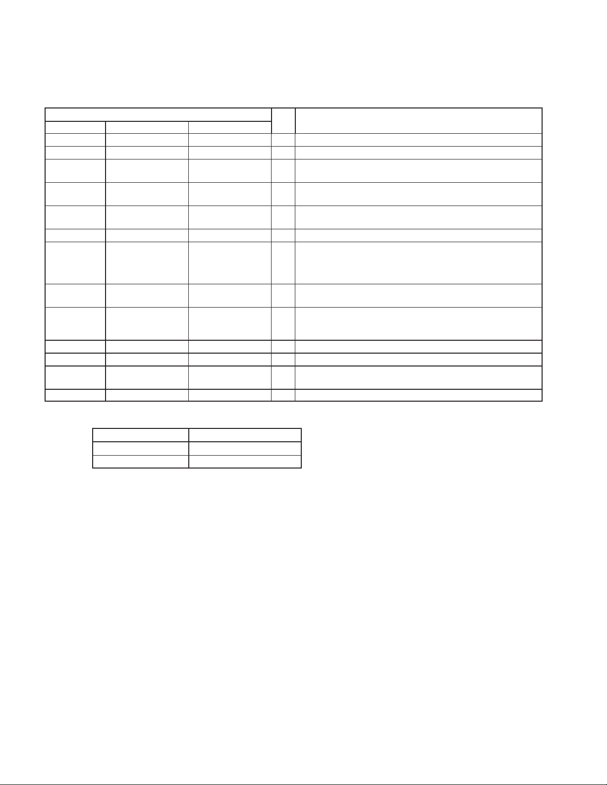
1.4.2 Microcontroller/Microprocessor Signals
I/O
DESCRIPTION
I/O
DESCRIPTION
TERMINAL
NAME PGE NO. GGW NO.
ALE 82 M15 I Address latch enable. Ignored when not DA mux mode
DA[15:0] 76, 74, 73, 72, 71,
69, 68, 65, 64, 62,
61, 60, 58, 57, 56, 55
M8M16 5 D1 I Bit width select. M8M16 determines the width of the data bus. The
MUXMODE 6 E3 I Mode selects. MUXMODE determines if the data and address lines are
XCS 84 M17 I Chip select
XINT 54 U9 O Interrupt
XRD 78 P17 I Read cycle enable
XWAIT 77 P16 O Wait
XWR 81 N17 I Write cycle enable
P15, R16, T17, U16,
T15, R14, U14, R12,
T12, R11, T11, U11,
T10, U10, T9, R9
(MUXMODE = 1).
I/O I/O lines used for address and data. See Table 2−1 for more
information on the use of address and data lines.
terminal is tied high for 16 bit mode. See Table 2−1 for more information
on the use of address and data lines.
parallel or multiplexed. The terminal is tied high for data address
multiplex mode. See Table 2−1 for more information on the use of
address and data lines.
1.4.3 Physical Layer
TERMINAL
NAME PGE NO. GGW NO.
CNA 135 C6 O Cable not active output. If no bias is detected from the cable, the CNA signal is
CONTEND 139 A4 I Contend. Tie high for bus manager capability.
CPS 142 A3 I Cable power supply . This terminal is normally connected to cable power through
FILTER0
FILTER1
LINKON 138 C5 O Link-on. The link-on output is activated if the LLC is inactive (LPS inactive or PD
LPS 130 A7 I Link power status. The signal indicates that the link is powered up and ready for
PD 136 A5 I Power-down input. When PD is asserted, the device is in a power down mode.
PWRCLS[2:0] 134, 133, 132 B6, A6, C7 I Power class inputs. See 1394a-2000 for more information. On hardware reset,
R0
R1
111
112
99
100
A15
A14
F17
F16
set high. The CNA output is not valid during power-up reset. CNA is valid during
power-down mode, when PD is high.
a 400-kΩ resistor. This circuit drives an internal comparator that is used to detect
the presence of cable power.
I PLL filter. These terminals are connected to an external capacitor to form a
lag-lead filter required for stable operation of the internal frequency multiplier PLL
running off the crystal oscillator. A 0.1-µF ±10% capacitor is the only external
component required to complete this filter.
active). The signal indicates that the PHY has detected a link-on packet
addressed to this node, or has detected a resume event on a suspended port.
The signal remains asserted until the LPS signal is asserted by the link in
response.
transactions. When this mode is deasserted, the device can be put into a low
power mode.
The device is asynchronously reset during this mode, so a device reset must be
provided after PD is deasserted. See Section 12 for more details.
these inputs set the default value on the power class indicated during self-ID.
Programming is done by tying terminals high or low.
Current setting resistor terminals. These terminals are connected to an external
resistance to set the internal operating currents and cable driver output currents.
—
A resistance of 6.34 kΩ ±1.0% is required to meet the IEEE Std 1394-1995
output voltage limits.
1−5
Page 16
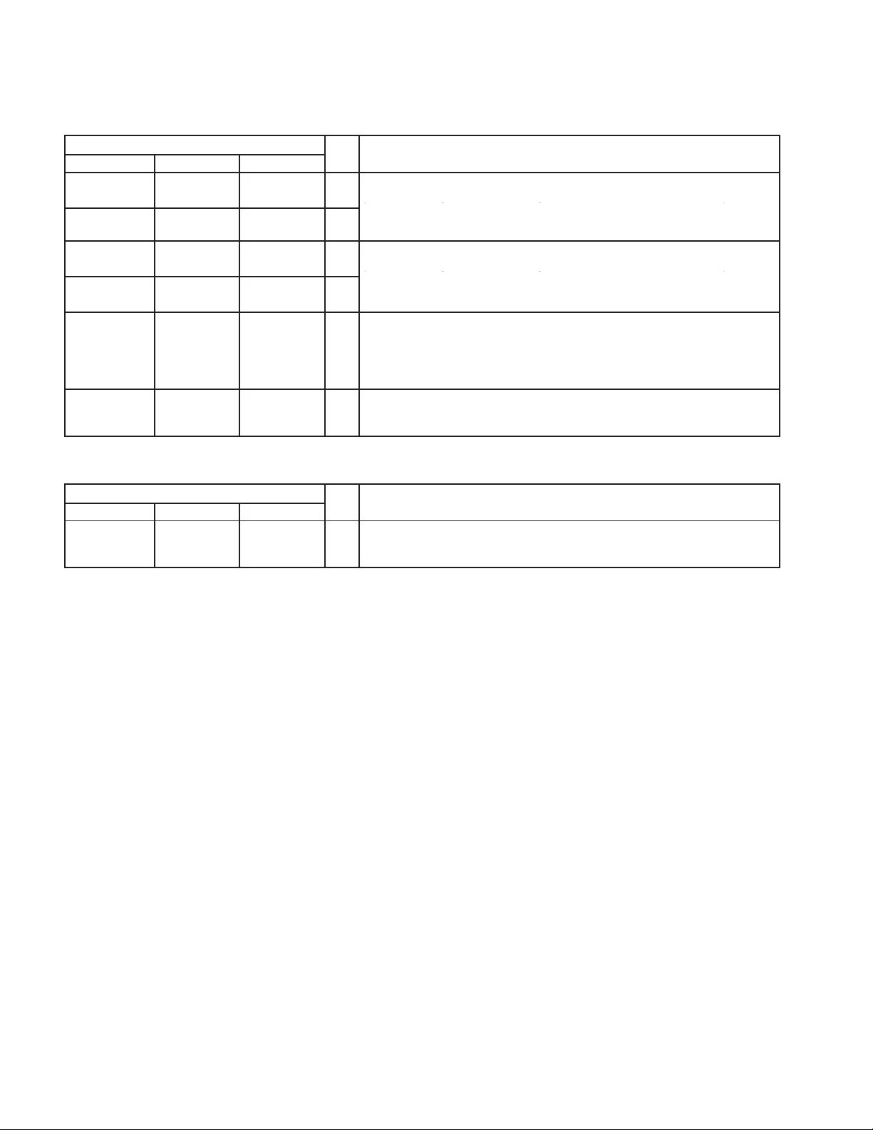
1.4.3 Physical Layer (continued)
I/O
DESCRIPTION
TPA1N
9596G17
I/O
Twisted-pair cable-A differential signal terminals. Board traces from each pair of
positive and negative differential signal terminals must match and be kept as
TPA2N
106
C17
I/O
TPB1N
9192J17
I/O
Twisted-pair cable-B differential signal terminals. Board traces from each pair of
positive and negative differential signal terminals must match and be kept as
TPB2N
102
E17
I/O
XO
116
A12
—
nant fundamental mode crystal. The optimum values for the external shunt ca-
I/O
DESCRIPTION
TERMINAL
NAME PGE NO. GGW NO.
TPA1N
TPA1P
TPA2N
TPA2P
TPB1N
TPB1P
TPB2N
TPB2P
TPBIAS1
TPBIAS2
XI
95
106
107
91
102
103
97
108
115
G17
G16
C17
C16
J17
J16
E17
E16
G15
B17
A13
1.4.4 Test Interface
TERMINAL
NAME PGE NO. GGW NO.
TEST[7:0] 129, 127, 125,
124, 122, 121,
120, 119
C8, A8, C9,
A9, C10, A10,
A11, B11
I/O Twisted-pair cable-A differential signal terminals. Board traces from each pair of
positive and negative differential signal terminals must match and be kept as
short as possible to the external load resistors and to the cable connector.
I/O
I/O Twisted-pair cable-B differential signal terminals. Board traces from each pair of
positive and negative differential signal terminals must match and be kept as
short as possible to the external load resistors and to the cable connector.
I/O
O Twisted pair bias output. This provides the 1.86-V nominal bias voltage needed
for proper operation of the twisted-pair cable drivers and receivers, and for
signaling to the remote nodes that there is an active cable connection. Each of
these terminals, except for an unused port, must be decoupled with a 1.0-µF
capacitor to ground. For the unused port, this terminal can be left unconnected.
Crystal oscillator inputs. These terminals connect to a 24.576-MHz parallel reso-
pacitors are dependent on the specifications of the crystal used.
I/O Test data lines. The test data lines are used in manufacturing test and is tied low in
normal/operational mode.
1−6
Page 17

1.4.5 Power Supplies
DESCRIPTION
TERMINAL
NAME PGE NO. GGW NO.
AGN[5:1] 109, 104, 98, 93, 90 A16, D17, G14, H17,
AVD[5:1] 110, 105, 101, 94, 89 B15, D16, F15, H16,
PWTST 15, 31, 47, 63, 80, 87,
118, 126, 141
VDD3V 10, 24, 33, 38, 52, 66,
70, 79, 128, 144
VDPLL 113 C13 PLL power supply. A combination of high-frequency decoupling capacitors
VSPLL 114 B13 PLL ground. These terminals must be tied together to the low-impedance
VSS 3, 11, 19, 27, 35, 43,
51, 59, 67, 75, 83, 88,
117, 123, 131, 140
B9, C4, C11, H3, L17,
P3, R8, T3, U13, U15
B4, B7, B10, D3, D11,
G3, K1, K17, M3, M16,
K16
K15
N16, P1, U6, U12
A2, B8, F2, L3, N15,
R2, R5, R10, R13,
R17, U8
Analog ground. These terminals must be tied together to the low-impedance
circuit board ground plane.
Analog circuit power terminals. A combination of high-frequency decoupling
capacitors near each terminal is suggested, such as paralleled 0.1-µF and
0.001-µF capacitors. These supply terminals are separated from PWTST,
VDD3V, and VDPLL internal to the device to provide noise isolation.
1.8-V Vdd power terminals. A combination of high-frequency decoupling
capacitors near each terminal is suggested, such as paralleled 0.1-uF and
0.001-uF capacitors. These supply terminals are separated from VDD3V,
AVD, and VDPLL internal to the device to provide noise isolation (this
voltage is not supplied when the internal regulator is enabled.)
3.3-V V
terminal is suggested, such as paralleled 0.1-uF and 0.001-µF capacitors.
These supply terminals are separated from PWTST, AVD, and VDPLL
internal to the device to provide noise isolation.
near each terminal is suggested, such as paralleled 0.1-µF and 0.001-µF
capacitors. These supply terminals are separated from PWTST, VDD3V,
and AVD internal to the device to provide noise isolation.
circuit board ground plane.
Digital ground. These terminals must be tied together to the low-impedance
circuit board ground plane.
A combination of high frequency decoupling capacitors near each
dd.
1.4.6 Miscellaneous
TERMINAL
NAME PGE
EN 32 P2 I/O/
MODE[2:0] 4, 2, 1 D2,
PHYTESTM 143 B3 I Test mode. This input terminal is used in manufacturing tests. Tie high during normal/operational
PLLON 137 B5 I PLL enable. This signal forces the internal phase-locked loop (PLL) on when it is asserted, even
XRESETL 85 L15 I Link reset. Reset for link block
XRESETP 86 L16 I PHY reset. Reset for PHY block
NO.
GGW
NO.
C1, B1
I/O DESCRIPTION
Internal 1.8-V regulator enable. This terminal enables the internal 1.8-V regulator. Tie low during
Hi-Z
normal/operational mode.
I Chip mode select. MODE[2:0] = 000 is the normal/operational mode. All other modes are for test
purposes and are not described in this data sheet.
mode.
during ultralow−power mode and power-down mode. If this signal is deasserted, the PLL operates
only during regular device operation.
1−7
Page 18

1.5 Terminal Assignments for TSB43AA82A
1.5.1 144-Terminal PGE Package
TERM.
NO.
1 MODE0 I 37 BDIO5 I/O 73 DA13 I/O 109 AGN5
2 MODE1 I 38 VDD3V 74 DA14 I/O 110 AVD5
3 VSS 39 BDIO6 I/O 75 VSS 111 FILTER0 I
4 MODE2 I 40 BDIO7 I/O 76 DA15 I/O 112 FILTER1 I
5 M8M16 I 41 BDACK I 77 XWAIT O 113 VDPLL
6 MUXMODE I 42 BDIO8 I/O 78 XRD I 114 VSPLL
7 BDITRIS I 43 VSS 79 VDD3V 115 XI I
8 BDICLK I 44 BDIO9 I/O 80 PWTST 116 XO
9 BDOCLKDIS I 45 BDIO10 I/O 81 XWR I 117 VSS
10 VDD3V 46 BDIO11 I/O 82 ALE I 118 PWTST
11 VSS 47 PWTST 83 VSS 119 TEST0 I/O
12 BDOCLK O 48 BDIO12 I/O 84 XCS I 120 TEST1 I/O
13 ATACK O 49 BDIO13 I/O 85 XRESETL I 121 TEST2 I/O
14 BDIF0 I 50 BDIO14 I/O 86 XRESETP I 122 TEST3 I/O
15 PWTST 51 VSS 87 PWTST 123 VSS
16 BDIF1 I 52 VDD3V 88 VSS 124 TEST4 I/O
17 BDIF2 I 53 BDIO15 I/O 89 AVD1 125 TEST5 I/O
18 BDOF0 O 54 XINT O 90 AGN1 126 PWTST
19 VSS 55 DA0 I/O 91 TPB1N I/O 127 TEST6 I/O
20 BDOF1 O 56 DA1 I/O 92 TPB1P I/O 128 VDD3V
21 BDOF2 O 57 DA2 I/O 93 AGN2 129 TEST7 I/O
22 BDIBUSY O 58 DA3 I/O 94 AVD2 130 LPS I
23 BDIEN I 59 VSS 95 TPA1N I/O 131 VSS
24 VDD3V 60 DA4 I/O 96 TPA1P I/O 132 PWRCLS0 I
25 BDOAVAIL O 61 DA5 I/O 97 TPBIAS1 O 133 PWRCLS1 I
26 BDOEN I 62 DA6 I/O 98 AGN3 134 PWRCLS2 I
27 VSS 63 PWTST 99 R0 I/O 135 CNA O
28 BDIO0 I/O 64 DA7 I/O 100 R1 I/O 136 PD I
29 BDIO1 I/O 65 DA8 I/O 101 AVD3 137 PLLON I
30 BDIO2 I/O 66 VDD3V 102 TPB2N I/O 138 LINKON O
31 PWTST 67 VSS 103 TPB2P I/O 139 CONTEND I
32 EN I 68 DA9 I/O 104 AGN4 140 VSS
33 VDD3V 69 DA10 I/O 105 AVD4 141 PWTST
34 BDIO3 I/O 70 VDD3V I 106 TPA2N I/O 142 CPS I
35 VSS 71 DA11 I/O 107 TPA2P I/O 143 PHYTESTM I
36 BDIO4 I/O 72 DA12 I/O 108 TPBIAS2 O 144 VDD3V
SIGNAL
NAME
I/O
TERM.
NO.
SIGNAL
NAME
I/O
TERM.
NO.
SIGNAL
NAME
I/O
TERM.
NO.
SIGNAL
NAME
I/O
1−8
Page 19

1.5.2 176-Terminal GGW Package
TERM.
NO.
A2 VDD3V C17 TPA2N I/O J14 NC R2 VSS
A3 CPS I D1 M8M16 I J15 NC R4 BDIO7 I/O
A4 CONTEND I D2 MODE2 I J16 TPB1P I/O R5 VSS
A5 PD I D3 VSS J17 TPB1N I/O R6 BDIO11 I/O
A6 PWRCLS1 I D7 NC K1 VSS R7 BDIO12 I/O
A7 LPS I D8 NC K2 BDOF1 O R8 VDD3V
A8 TEST6 I/O D9 NC K3 BDOF2 O R9 DA0 I/O
A9 TEST4 I/O D10 NC K4 NC R10 VSS
A10 TEST2 I/O D11 VSS K14 NC R11 DA6 I/O
A11 TEST1 I/O D15 NC K15 AVD1 R12 DA8 I/O
A12 X0 D16 AVD4 K16 AGN1 R13 VSS
A13 X1 I D17 AGN4 K17 VSS R14 DA10 I/O
A14 FILTER1 I E1 BDICLK I L1 BDIBUSY O R16 DA14 I/O
A15 FILTER0 I E2 BDITRIS I L2 BDIEN I R17 VSS
A16 AGN5 E3 MUXMODE I L3 VDD3V T1 BDIO4 I/O
B1 MODE0 I E15 NC L4 NC T3 VDD3V
B3 PHYTESTM I E16 TPB2P I/O L14 NC T4 BDACK I
B4 VSS E17 TPB2N I/O L15 XRESETL I T5 BDIO9 I/O
B5 PLLON I F1 NC L16 XRESETP I T6 NC
B6 PWRCLS2 I F2 VDD3V L17 PWTST T7 BDIO13 I/O
B7 VSS F3 BDOCLKDIS I M1 BDOAVAIL O T8 BDIO15 I/O
B8 VDD3V F15 AVD3 M2 BDOEN I T9 DA1 I/O
B9 PWTST F16 R1 I/O M3 VSS T10 DA3 I/O
B10 VSS F17 R0 I/O M15 ALE
B11 TEST0 I/O G1 ATACK O M16 VSS T12 DA7 I/O
B12 NC G2 BDOCLK O M17 XCS I T13 NC
B13 VSPLL G3 VSS N1 BDIO0 I/O T14 NC
B14 NC G4 NC N2 BDIO1 I/O T15 DA11 I/O
B15 AVD5 G14 AGN3 N3 BDIO2 I/O T17 DA13 I/O
B17 TPBIAS2 O G15 TPBIAS1 O N15 VDD3V U2 BDIO5 I/O
C1 MODE1 I G16 TPA1P I/O N16 PWTST U3 BDIO6 I/O
C2 NC G17 TPA1N I/O N17 XWR I U4 BDIO8 I/O
C4 PWTST H1 BDIF0 I/O P1 PWTST U5 BDIO10 I/O
C5 LINKON O H2 BDIF1 I/O P2 EN I U6 PWTST
C6 CNA O H3 PWTST P3 VDD3V U7 BDIO14 I/O
C7 PWRCLS0 I H4 NC P7 NC U8 VSS
C8 TEST7 I/O H14 NC P8 NC U9 XINT O
C9 TEST5 I/O H15 NC P9 NC U10 DA2 I/O
C10 TEST3 I/O H16 AVD2 P10 NC U11 DA4 I/O
C11 PWTST H17 AGN2 P11 NC U12 PWTST
C12 NC J1 BDIF2 I/O P15 DA15 I/O U13 VDD3V
C13 VDPLL J2 NC P16 XWAIT O U14 DA9 I/O
C14 NC J3 BDOF0 O P17 XRD I U15 VDD3V
C16 TPA2P I/O J4 NC R1 BDIO3 I/O U16 DA12 I/O
SIGNAL
NAME
I/O
TERM.
NO.
SIGNAL
NAME
I/O
TERM.
NO.
SIGNAL
NAME
I/O
TERM.
NO.
T11 DA5 I/O
I
SIGNAL
NAME
I/O
1−9
Page 20

1−10
Page 21
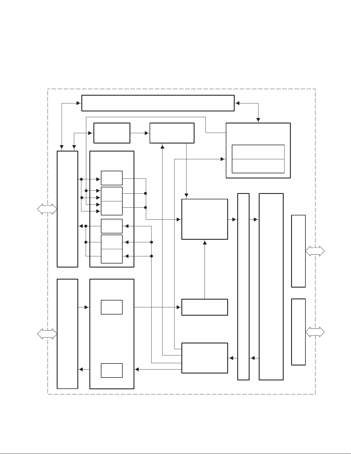
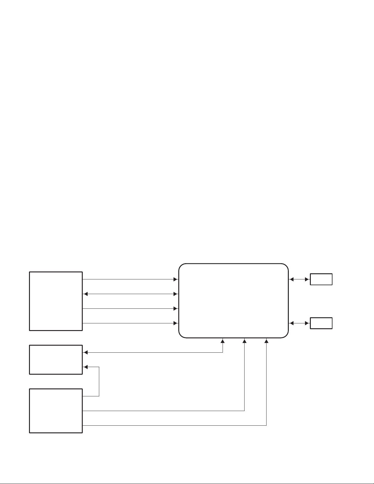
2 Architecture
The iSphynx II functional block architecture is shown in Figure 2-1.
Configuration Register (CFR)
8/16
Host
I/F
Configuration
ROM
Asynchronous
Command FIFO
ATF
MTQ
CTQ
ARF
MRF
CRF
BDFIFO
Auto
Response
(AR)
Transaction
Timer/Manager
(TrMgr)
Fast ORB
Exchanger (FOX)
MOAF_AGENT
COAF_AGENT
LOG
Link
Core
(1394a)
Port
2
8/16
DMA
(Bulky
Data)
I/F
DTF
DRF
Packetizer
Packet
Distributor
Figure 2−1. Functional Block Architecture
Port
1
2−1
Page 22
2.1 Host I/F
The host (microcontroller) interface is the interface between the microcontroller, the CFR, the asynchronous
command FIFOs, and the ConfigROM. The host bus interface consists of an 8-bit data bus and an 8-/16-bit address
bus. The TSB43AA82A is interrupt driven to reduce polling. This interface has endian programmable access, and
allows the microcontroller easy access to the CFR. See Section 10 for more details.
Table 2−1. Address/Data
M8M16 MUXMODE Data Address
0 (8-bit) 0 (parallel) DA[15:8] DA[7:0]
1(MUX) DA[7:0] DA[7:0]
1 (16-bit) 0 (parallel) DA[15:0] BDIO[15:8]
1(MUX) DA[15:0] DA[7:0]
2.2 DMA I/F (Bulky Data I/F)
The DMA bulky interface provides a data transfer interface for high-speed peripherals. It is the interface between an
external host DMA and the DMA FIFO (BDFIFO). The interface provides up to 160-Mbps sustained data rates. The
bulky data interface supports several modes such as 8-bit or 16-bit parallel width and asynchronous/synchronous
modes. See Section 9 for more details.
2.3 Configuration Register (CFR)
The configuration register (CFR) is the internal register for controlling and managing the TSB43AA82A operation.
It provides most of the control bits and host controller monitor. The CFR is discussed in detail in Section 3.
2.4 Fast ORB Exchanger (FOX)
The fast ORB exchanger or FOX module supports management ORB and command block ORB transactions. In the
SBP-2 protocol, the target has to read ORB packets from initiators. When requested by the initiator , the FOX module
automatically reads the management ORB and command block ORB. Linked command-block ORBs are
automatically fetched one by one and the hardware supports up to four agents. The management ORB and the
command-block ORB each have two FIFO modules for transmit and receive. See Section 7 for more details.
• MOAF_AGENT: Management ORB auto-fetch agent. Controls fetch/state for management ORB.
• COAF_AGENT: Command-block ORB auto-fetch agent. Fetches command block ORBs and manages
command block agent registers.
2.5 Auto Response (AR)
The auto response (AR) module provides the auto packet response service for incoming request packets. The AR
services configuration ROM read requests, agent-state read requests, and unexpected packets.
2.6 Transaction/Timer Manager (TrMgr)
The transaction/timer manager module provides transaction control service for transmit priority between control
packets and data packets. Any cable packet transmit request is sent in the order the request is received. This module
also manages split transactions and controls busy retry. See Section 6 for more details.
2−2
Page 23

2.7 Packet Distributor
The packet distributor module provides the packet routing service for each FIFO module. In SBP-2 mode, all request
and response packets are properly routed to the correct FIFO, and sent to corresponding initiators. In direct print
protocol (DPP) mode, the packet distributor filters a request packet by its address and then saves it into the correct
receive FIFO.
2.8 Packetizer
The packetizer module provides packetization for a transmit packet. The data stream from the DMA FIFO is split into
small packets that meet the SBP-2 requirements. A read or write request header is attached to each packet with a
correctly incremented destination address. The transaction/timer manager provides busy retry and split transaction
timer control if required. The packetizer also provides auto-page table fetch service. The internal auto-fetch module
sends a read request to the present page address, and the DMA automatically sends data to the requested address
set by the Page Table Element. At the end of packetizer , if the DMA function has successfully completed, the DMA
automatically sends a status block packet.
2.9 Configuration ROM
The ConfigROM provides the configuration ROM required by the IEEE 1212 standard2. The ConfigROM module
supports the auto response service for a ConfigROM read request and records the transaction history. The host
controller can load ConfigROM data during node initialization. Once initialized, the ConfigROM is accessible by peer
node read requests. See Section 5 for more details.
2.10 Link Core
The link core provides link layer service such as correctly formatted IEEE 1394-19953 and IEEE 1394a-2000
asynchronous transmit and receive packets. It also generates and inspects the 32-bit cyclic redundancy check
(CRC). This link core does not support isochronous service.
2.11 PHY (and PHY Interface)
The TSB43AA82A has an integrated 400-Mbps two-port physical layer. The PHYsical (PHY) interface provides
PHY-level service to the link layer service. See Section 11 for more details.
2.12 FIFOs
The TSB43AA82A has three FIFO types, asynchronous command FIFOs, configuration ROM FIFOs and DMA
FIFOs. These FIFO types have maximum sizes of 378 quadlets, 126 quadlets, and 1182 quadlets respectively.
Except for the MTQ and MRF, the FIFO sizes are adjustable. The sum of all the FIFOs in a type must not exceed the
maximum size. See Section 4 for more information on the asynchronous command FIFOs, Section 5 for more
information on ConfigROM/LOG FIFOs, and Section 8 for more information on BDFIFOs.
4
2
IEEE Std 1212-1991, IEEE Standard Control and Status Register (CSR) Architecture for Microcomputer Buses
3
IEEE Std 1394-1995, IEEE Standard for a High Performance Serial Bus
4
IEEE Std 1394a-2000, IEEE Standard for a High Performance Serial Bus - Amendment 1
2−3
Page 24
Asynchronous command FIFOs (total 378 quadlets)
MTQ:
MRF:
CTQ:
CRF:
ATF:
ARF:
Management ORB transmit FIFO
Management ORB receive FIFO
Command block ORB transmit FIFO
Command block ORB receive FIFO
Asynchronous packet transmit FIFO
Asynchronous packet receive FIFO
3 quadlets (fixed)
15 quadlets (fixed)
Adjustable
Adjustable
Adjustable
Adjustable
ConfigROM/LOG FIFOs (total 126 quadlets)
Autoresponse ConfigROM area
Page table buffer for DTF
Page table buffer for DRF
Status block buffer for DTF
Status block buffer for DRF
Log data area
Adjustable
Adjustable
Adjustable
Adjustable
Adjustable
Adjustable
DMA FIFOs (BDFIFO) (total 1182 quadlets)
DTF:
DRF:
Data transmit FIFO
Data receive/fetch FIFO
Adjustable
Adjustable
2.13 Example System Block Diagrams
2.13.1 Asynchronous Mode With Separate Microcontroller and DMA Bus
In this system, the CPU has no DMA capabilities. At the host I/F of the TSB43AA82A is a CPU with no DMA
capabilities. At the DMA I/F of the TSB43AA82A is a DMA controller to control the data in and out of the
TSB43AA82A.
CPU
Memory
DMA Controller
ADDR
Data 8 or 16
WR
RD
Data 8 or 16
ADDR
DA
XWR
XRD
1394
TSB43AA82A
1394
BDIO BDIEN BDOEN
2−4
Page 25
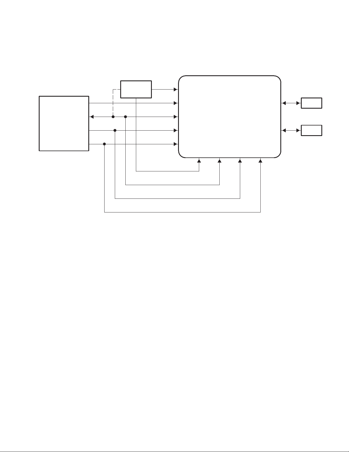
2.13.2 SCSI Mode With Shared Microcontroller and DMA Bus
In this system, the host I/F and the DMA I/F of the TSB43AA82A share the same data and control buses. The
CPU has DMA capabilities and the address decode is used to determine which I/F is addressed by the CPU.
CPU
ADDR
Data
WR
RD
Address
Decode
CS
CS
XCS
ADDR
DA
XWR
XRD
BDACK BDIO BDWR BDRD
TSB43AA82A
1394
1394
2−5
Page 26

2−6
Page 27
3 Configuration Register (CFR)
The CFR contains the registers that dictate the basic operation of the TSB43AA82A. A CFR map is shown in
Table 3-1. These registers default to 0 and are unaffected by a bus reset unless otherwise specified.
3.1 Addressing
The CFR is addressed in bytes. The address terminal order is described below:
Address[7:0] = (DA7, DA6, DA5, DA4, DA3 , DA2, DA1, DA0)
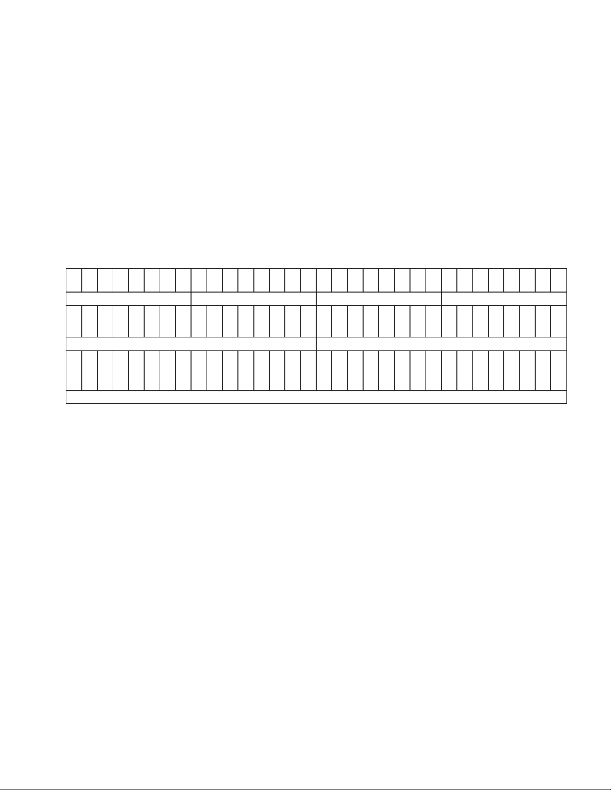
3.2 Data Bit/Byte Order
MSB LSB
1 2 3 4 5 6 7 8 9 1011121314151617181920212223242526272829303
0
Byte0 Byte1 Byte2 Byte3
D
D
D
D
D
D
D
D
D
D
D
D
D
D
D
D
D
D
D
D
D
D
D
D
D
D
D
D
D
A
A
A
A
A
A
A
A
A
A
A
A
A
A
A
A
A
A
A
A
A
A
A
A
A
A
A
7
6
5
4
3
2
1
0
7
6
5
4
3
2
1
0
7
6
5
4
3
2
1
0
7
6
Doublet0 Doublet1
D
D
D
D
D
D
D
D
D
D
D
D
D
D
D
D
D
D
D
D
D
D
D
D
D
A
A
A
A
A
A
A
A
A
A
A
A
A
A
A
A
A
A
A
A
A
A
A
1
1
1
1
1
1
9
8
7
6
5
4
3
2
1
0
1
1
1
1
1
5
4
3
2
1
0
5
Quadlet
4
3
2
1
1
0
A
9
8
D
A
A
7
6
A
5
4
D
D
A
A
5
4
D
A
A
3
2
D
D
A
A
3
2
1
D
D
A
A
1
0
D
D
A
A
1
0
3−1
Page 28
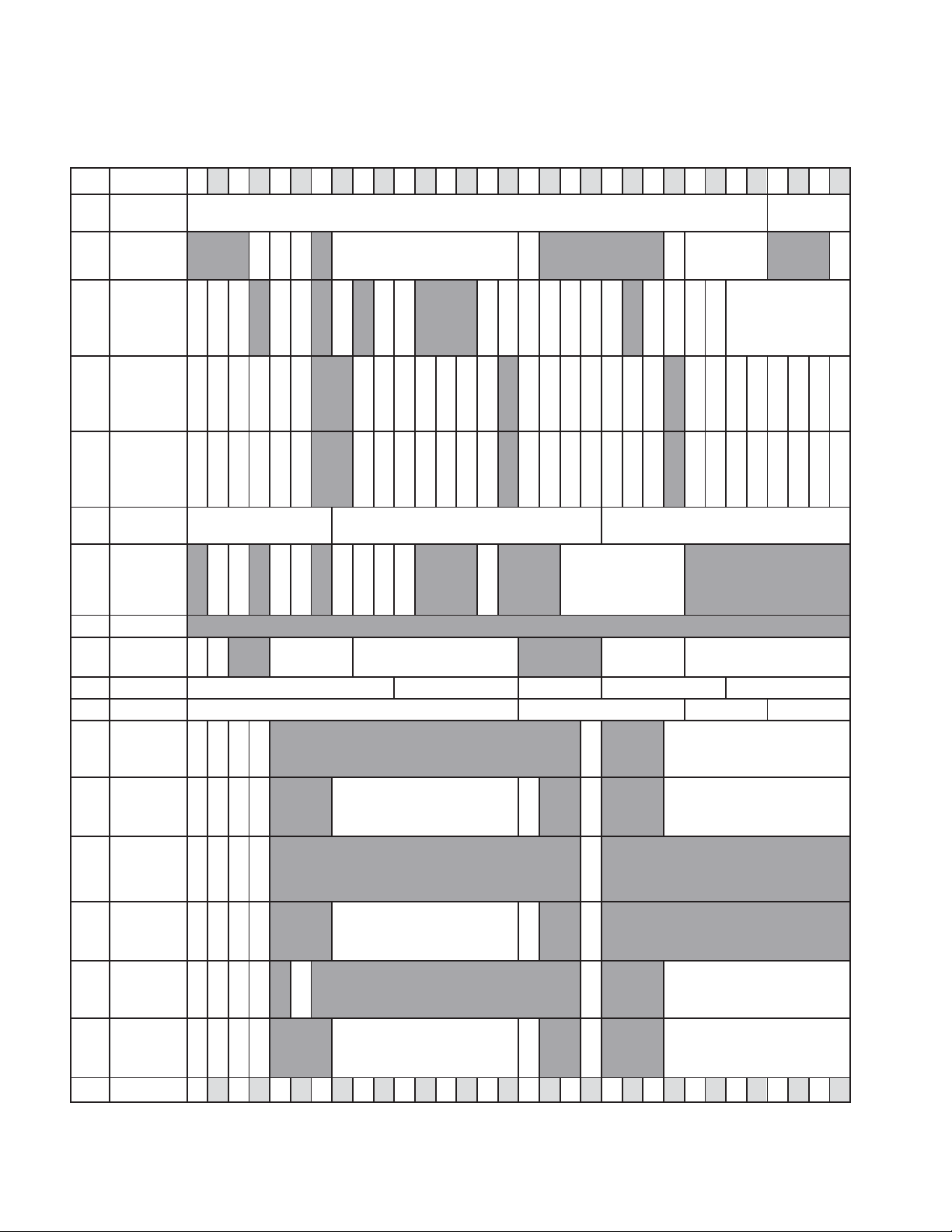
00h
04h
Version/
Revision
Miscellaneous
Table 3−1. CFR Map
0
1
2
3
4
5
6
7
8
9
C
LPS
LKON
101112131415161718192021222324252627282930
Version Revision
Ping_Timer
Root
ATAck
AckErr
31
AckVld
08h Control
0Ch Interrupt
Interrupt
10h
Mask
Cycle
14h
Timer
18h Diagnostics
1Ch Reserved
PHY
20h
Access
24h Bus Reset BusNumber NodeNum BRFErr_Code NodeSum CFRContID
28h Time Limit SplitTimeOut RetryInterval RtryLmt ORBTimer
2Ch ATF Status
IDVal
RxSld
Int
PhInt
Int
PhInt
Seconds_Count Cycle_Count Cycle_Offset
ACKTardy
WrPy
RdPy
ATFFul
ATFAFl
Bsy0
RSIsel
Breset
Breset
BudgEn
ATFAEm
TrEn
ACArbOn
Endslf
Phypkt
CmdSlf
Endslf
Phypkt
CmdSlf
RegRW
PhyRgAd PhyRgData PhyRxAd PhyRxData
ATFEmp
AgRdy0
AgntStWr
BDIFcntEN
SntRj
PhRRx
SntRj
PhRRx
AgRdy1
AgRdy2
RstTr
IFAcc
HdrErr
IFAcc
HdrErr
AgRdy3
TCErr
CySec
TCErr
CySec
StErpkt
SplTrEn
ErrResp
Cyst
DRHUpdate
Cyst
DRHUpdate
MAAckconf
RetryEn
Ackpnd
MAAckConf
FaGap
TxRdy
CyDne
FaGap
TxRdy
CyDne
Budget_Counter
ATFClr
CyMas
CyLst
CyPnd
CyLst
CyPnd
DMclr
CyTmrEn
CyArbF
CyArbF
RxUnexp
ATFEnd
ATFEnd
Prio_Budget
RUEsel
ARFRxd
MOREnd
ARFRxd
MOREnd
ATF_Size
DTFEnd
COREnd
DTFEnd
COREnd
TxExpr
DRFEnd
TxExpr
DRFEnd
AgntWr
AgntWr
30h ARF Status
MTQ
34h
Status
MRF
38h
Status
CTQ
3Ch
Status
40h CRF Status
3−2
ARFFul
ARFAFl
MTQFul
MTQAFl
MRFFul
MRFAFl
CTQFul
CTQAFl
CRFFul
CRFAFl
0
1
ARFEmp
ARFAEm
MTQEmp
MTQAEmp
MRFEmp
MRFAEm
CTQAEm
CTQEmp
CRFEmp
CRFAEm
2
3
4
ARFThere
ARFCD
MRFThere
MRFCD
CTQ1Av
CRFThere
CRFCD
5
6
7
8
9
101112131415161718192021222324252627282930
ARFClr
MTQClr
MRFClr
CTQClr
CRFClr
ARF_Size
CTQ_Size
CRF_Size
31
Page 29
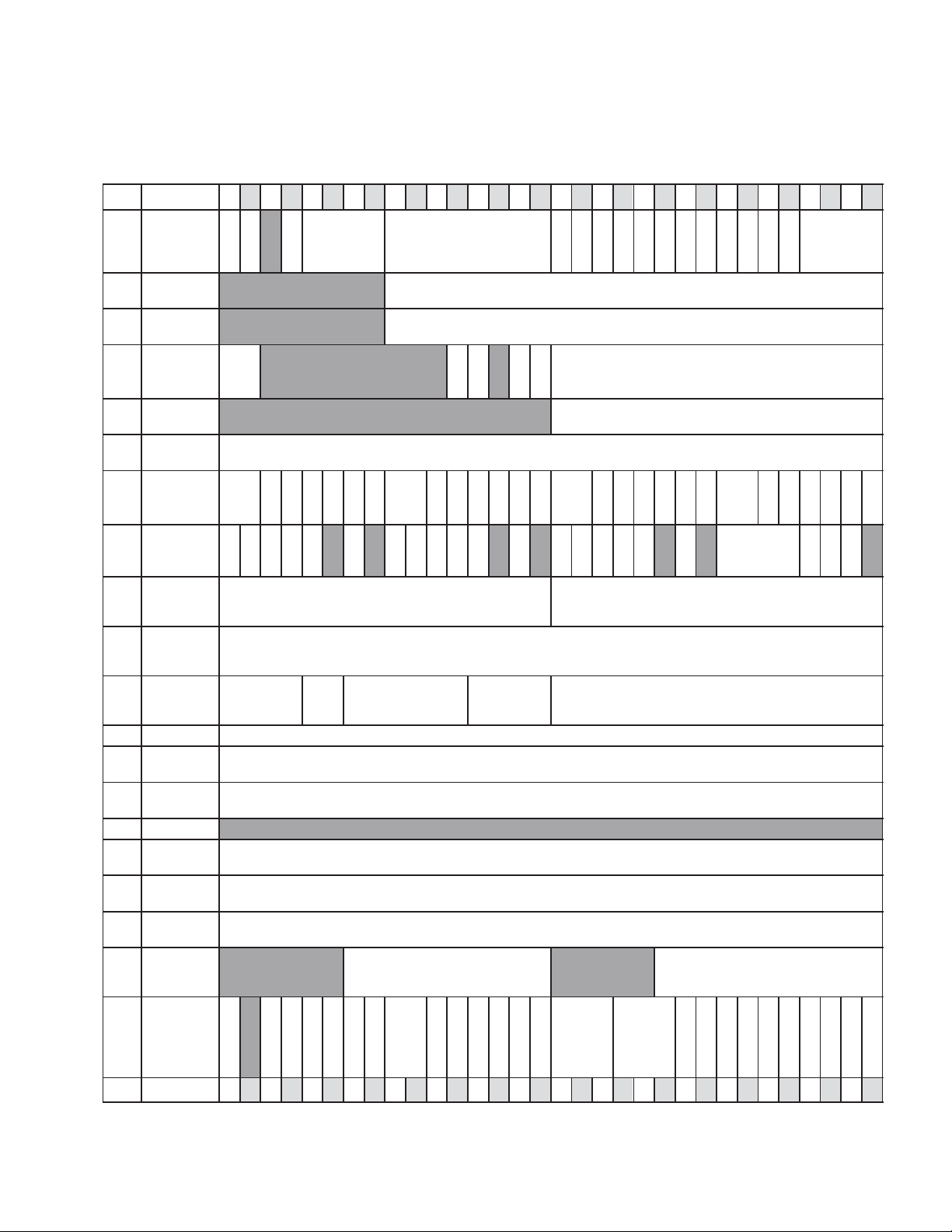
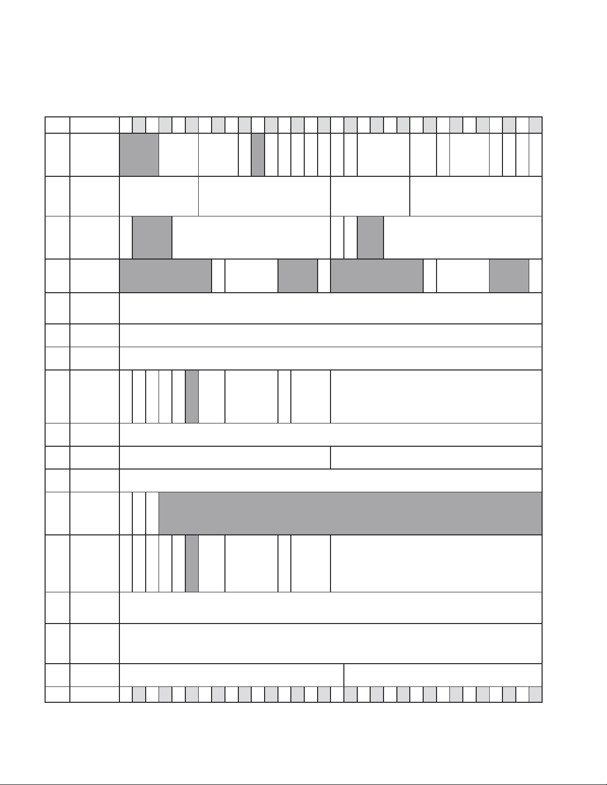
Table 3−1. CRF Map (Continued)
Retry_Counter
p
0
1
2
3
4
5
6
7
8
9
101112131415161718192021222324252627282930
31
ORB Fetch
44h
Control
Manage-
48h
ment Agent
Command
4Ch
Agent
Agent
50h
Control
ORB
54h
Pointer 1
ORB
58h
Pointer 2
Agent
5Ch
Status
Transaction Timer
60h
Control
Transac-
tion Timer
64h
Status 1
Transac-
tion Timer
68h
Status 2
Transac-
tion Timer
6Ch
Status 3
70h Write-First Write_First
Write-
74h
Continue
Write-
78h
Update
7Ch Reserved
ARF Data
80h
Read
MRF Data
84h
Read
CRF Data
88h
Read
Configura-
tion ROM
8Ch
Control
MAgtVld
MAgtBsy
AgtNmb
State0
DTTxEd
DRTxEd
tCode Spd tLabel
MShtFmt
DrBll0
UnStEn0
ATTxEd
MTTxEd
MORB_Prior
Rst0
Dead0
DrBClr0
USEClr0
CTTxEd
ARTxEd
Destination_ID Destination_offset_hi
CORB_Size
Management_Agent_offset
WrNdId
AgntVld
USTIEn
ORB_destination_offset_lo
State1
DTErr
DRErr
AR_CSR_Size CSR_Size
DrBll1
ATErr
Dead1
UnStEn1
CTErr
MTErr
Destination_offset_lo
RdNdID
Rst1
DrBClr1
USEClr1
ARErr
Write_Continue
Write_Update
ARFRead
MRFRead
CRFRead
CAg0Vld
CAg1Vld
CAg2Vld
CAg3Vld
Agent_base_offset
DrBll2
State2
DTRtry
ATRtry
DRRtry
UnStEn2
MTRtry
DrBSnp
DrBFtEn
CnxFtEn
CShtFmt
CAg0Rdy
CAg1Rdy
CAg2Rdy
Agent_NodeID
ORB_destination_offset_hi
Rst2
Dead2
CTRtry
DrBClr2
USEClr2
ARRtry
SplitTrTimer
State3
TimrNo
DrBll3
CORB_Prior
CAg3Rdy
Rst3
Dead3
UnStEn3
HldTr
TxAbrt
DrBClr3
USEClr3
RlsTr
90h
DMA
Control
DRPage-
DTFEn
DRFEn
DMARW
0
1
2
3
DTPktz
DRPktz
4
5
DTSpDis
DRSpDis
6
7
DhdSel
8
LongBlk
QuadSend
RconfSnglpkt
9
101112131415161718192021222324252627282930
QuadBndry
FetchSiz
AutoPg
CheckPg
DTPageFetchSiz
Dackpnd
Drespcm
DTHdls
Dpause
DRHStr
DRStPS
DTDSel
DRDSel
DTFClr
DRFCLr
31
3−3
Page 30
94h
tl
BDIMode
rr
al
rr
DTF Page
DRF Page
98h
Bulky
Interface
Control
DTF/DRF
and DTF/
DRF Page
Table Size
Table 3−1. CRF Map (Continued)
0
1
2
3
4
5
6
7
8
9
101112131415161718192021222324252627282930
BDIDelay
BLECtl
BOAvCtl
BIEnC
BOEnCtl
AutoPad
MTRBufSiz
DTFPTBufSiz DTF_Size DRFPTBufSiz DRF_Size
MTTBufSiz
BlBsyCtl
ATAckCtl
BDAckCtl
Burst
BDOMode
RcvPad
BDORst
31
BDIRst
BDOTris
9Ch
A0h
A4h
A8h
ACh
B0h
B4h
B8h
BCh
C0h
DTF/DRF
Available
DTF/DRF
Acknowl-
edge
DTF First
and
Continue
DTF
Update
DRF Data
Read
DTF
Control 0
DTF
Control 1
DTF
Control 2
DTF
Control 3
DRF
Control 0
(direct)
DTFEmpty
DTFCTL0
DTFCTL1
DTFClr/DTFst
DRFBldEn
DRFSldEn
DRFAdrEn
DTFNotify
DTFNdldval
DTF_destination_ID
DTFAvail
DRxAck
DRAE
DTF Max
Payload
DTF Spd
BDOAvail
DRFEmpty
DRAV
DTF_First&Continue
DTF_Update
DRFRead
Size
PgTblEn
DTF_BlockCount/DTF_BlockSize
DTF_destination_offset_lo
DTF_BlockSize/DTF_BlockCount
DRFThere
DTxAck
DTAE
DTF_destination_offset_hi
DTAVal
3−4
C0h
C4h
C4h
C8h
DRF
Control 0
(packetiz-
er)
DRF
Control 1
(direct)
DRF
Control 1
(packetiz-
er)
DRF
Control 2
DRFCTL0
DRFCTL1
DRFClr/DRFst
0
1
2
DRFNotify
DRFNdIdVal
DRF_destination_ID
3
4
5
DRFSpd
6
7
DRF Max
Payload
DRF_BlockCount/DRF_BlockSize
8
9
101112131415161718192021222324252627282930
Size
PgTblEn
DRF_destination_Width
DRF_BlockSize/DRF_BlockCount
DRF_destination_offset_hi
31
Page 31

CCh
DTxRt
E8h
DRxRt
D0h
D4h
D8h
DCh
DRF
Control 3
DRF
Header 0
DRF
Header 1
DRF
Header 2
DRF
Header 3
Table 3−1. CRF Map (Continued)
0
1
2
3
4
5
6
7
8
9
101112131415161718192021222324252627282930
DRF_destination_offset_lo
DRF_Header0
DRF_Header1
DRF_Header2
DRF_Header3
31
E0h
E4h
ECh
F0h
DRF
Trailer
DTF/DRF
Page
Count
DhdSel=00
DTx
Header 0
DhdSel=01
DTx
Header 0
DhdSel=10
DRx
Header 0
DhdSel=11
DRx
Header 0
DhdSel=00
DTx
Header 1
DhdSel=01
DTx
Header 1
DhdSel=10
DRx
Header 1
DhdSel=11
DRx
Header 1
DhdSel=00
DTx
Header 2
DhdSel=01
DTx
Header 2
DhdSel=10
DRx
Header 2
DhdSel=11
DRx
Header 2
STAT RESP
STAT RESP
0
1
2
3
4
Fll0 DRF_TxAck
Rx_Spd
DTF Page Count DRF Page Count
DTxtLabel
DTxSpd
Ack PSTAT PRESP
AckErr
DRxtLabel
DRxSpd
Ack PSTAT PRESP
AckErr
DTx_destination_ID DTx_destination_offset_hi
DTx page number
DRx_destination_ID DRx_destination_offset_hi
DRx page number
DTx_destination_offset_lo
DTx page length DTx page table hi
DRx_destination_offset_lo
DRx page length DRx page table hi
5
6
7
8
9
101112131415161718192021222324252627282930
DTxtCode
DRxtCode
DTxPrio
PAck
PAckErr
DRxPrio
PAck
PAckErr
31
3−5
Page 32

F4h
Q
F
lr
F8h
DhdSel=00
DTx
Header 3
DhdSel=01
DTx
Header 3
DhdSel=10
DRx
Header 3
DhdSel=11
DRx
Header 3
Table 3−1. CRF Map (Continued)
0
1
2
3
4
5
6
7
8
9
101112131415161718192021222324252627282930
DTx_data_length DTx_extended_tCode
DTx page table lo
DRx_data_length DRx_extended_tCode
DRx page table lo
31
FCh
Log/ROM
Control
(XLOG=0)
Log/ROM
Control
(XLOG=1)
Log ROM
Data
LogATF
LogARF
DTFSt
DRFSt
0
1
LogMRF
LogMTQ
LogMAgnt
2
3
4
LogAgnt
LogCT
5
6
LogCR
LogDTFRq
7
8
XLOG
LogC
ShortLog
LogDTFRs
LogDRFRq
9
101112131415161718192021222324252627282930
LogRetry
LogDRFRs
LogARROM
LogRead/ROMAccess
ROMValid
XLOG
ROMValid
LogCD
LogFull
LogThere
/
ROMAddr
Adder
3.3 Write/Read Access
The CFR can be addressed in bytes. The host (microcontroller) has only quadlet write/read access to the CFR. To
write to a byte/doublet requires a quadlet write. To read a byte/doublet requires a quadlet read. The host I/F defaults
to a little endian state. See Sections 3.4.1 and 9.4 for more information on CFR endianess.
3.4 CFR Definitions
DIR : Direction of register access
R/O: Read-only
R/W: Read/write
W/O: Write-only
S/C: Set by a write of one and then cleared by a write of one.
N/A: The host obtains a meaningless value when it reads from or writes to the bit.
Default: Value after a power-on reset
NOTE:
Unless otherwise specified, the field values are 0 after a power-on reset (default) and a bus
reset. When the values differ, the two initial values are explicitly noted.
31
3.4.1 Version/Revision Register at 00h
The version/revision register defines the TI device code name of the TSB43AA82A. This register also determines
the endianness of the host I/F. The host I/F defaults to a little endian state. To swap the endianness of the host I/F
to big endian (example: [0382 0043] >[4300 8203]), write FFFF FFFFh to this address. To swap the endianness of
the host I/F to little endian mode, write 0000 0000h.
BITS ACRONYM DIR DESCRIPTION
0-27 Version R/W The version is fixed to 4300 820h.
28-31 Revision R/W The revision is fixed to 3h.
3−6
Page 33

3.4.2 Miscellaneous Register at 04h
This register defaults to 1400 0000h and, except for the bits specified, is cleared on a bus reset.
BITS ACRONYM DIR DESCRIPTION
0-2 Reserved N/A Reserved
3 C R/O Bus manager capable. This bit is active when the PHY is ON even when the link is in reset. The bit defaults
4 LKON S/C Link-on output from PHY. This bit is active when the PHY generates the LINKON signal, even when the link
5 LPS R/O Link power status. Setting this bit to 1 sets the internal PHY LPS signal to one. This bit defaults to 1 and is
6 Reserved N/A Reserved
7-15 Ping_Timer R/O Ping timer value. The timer measures the time in units from when a ping packet is transmitted to when the
16 Root R/O Root state of the local PHY. This bit indicates whether the node is the root node. The root bit is set to 1 when
17-22 Reserved N/A Reserved
23 AckErr R/O Acknowledge error. The AckErr bit is set when the ack received for the packet transmitted from the ATF
24-27 ATAck R/O Address transmitter acknowledges received. These bits contain the last ack received in response to a
28-30 Reserved N/A Reserved
31 AckVld R/O Acknowledge valid. This bit is 1 when the AT Ack has not been read and is cleared to 0 when the ATAck is
to 1 and is is unaffected by a bus reset. This bit is determined by the CONTEND terminal defined in Section
2.
is in reset. This bit is set when the PHY detects a LINKON packet. This bit defaults to 0 and is unaffected by
a bus reset.
unaffected by a bus reset. Refer to Section 11 for more detail.
ping response is received. One unit is 40ns.
the node is root. This bit defaults to 0 and is automatically set by the hardware.
has a parity or length error.
packet sent by the ATF. This value is updated each time an ack is received.
read.
3.4.3 Control Register at 08h
This register defaults to 4400 CA00h and is unaffected by a bus reset.
BITS ACRONYM DIR DESCRIPTION
0 IDVal R/O ID valid. The IDVal bit is set to 1 when the information of the bus reset register at 24h is valid. This bit
1 RxSId R/W Receive self-identification (self-ID) packets. When set to 1, the self-ID packets generated by the PHY
2 RSIsel R/W Received self-ID packet location selection. If RxSId is set to 1, the received self-ID packets are verified and
3 Reserved N/A Reserved
4 Bsy0 R/W Busy control. When this bit is set to 1, the ack_busy_X is sent to all incoming packets. When Bsy0 is set to
5 TrEn R/W Transactions enable. When TrEn is set to 1, the transmitter and receiver are enabled to transmit and
6 Reserved N/A
7 ACArbOn R/W Accelerated arbitration on. When ACArbOn is set to 1, accelerated arbitration is enabled.
8 Reserved N/A Reserved
9 BDIFcntEN N/A BDIF control enable. When BDIFcntEN is set to 1, ATACK, BDOAVAIL, BDIBUSY and BDOF[2:0] are
10 RstTr S/C Reset transaction. When RstTr i s set to 1, the entire transaction in the ATF, the ARF, the CTQ, the CRF, the
11−13 Reserved N/A Reserved
14 ErrResp R/W Error packet response. When ErrResp is set to 1, packets with errors are returned an ack_pending in the
defaults to 0 and is automatically set by the hardware on a bus reset.
during bus initialization are received and written to DRF or LOG as individual packets. Otherwise the
self-ID packets are not received. This bit defaults to 1 and is unaffected by a bus reset.
written to the DRF when RSIsel is set to 1 and are verified and written to the LOG when RSIsel is set to 0.
0, ack_busy_X is sent according to the normal busy/retry protocol.
receive packets. When TrEn is set to 0, the link core is not awake, the TSB43AA82A cannot send ack or
receive self-ID packets, and the transmitter and receiver are disabled. This bit defaults to 1 and is
unaffected by a bus reset.
Reserved
placed in the high-impedance state.
MTQ, and the MRF resets synchronously. This does not affect the DTF and the DRF.
response packet. When ErrResp is set to 0, packets with errors are returned an ack error code in the
response packet.
3−7
Page 34

BITS
15 StErpkt R/W Store error packets. When StErpkt is set to1, packets with any errors are stored.
16 SplTrEn R/W Split transaction enable. When SplTrEn is set to 1, split transactions are enabled. The ATF timer attempts a
17 RetryEn R/W Automatic retry enable. When set to 1, the ATF retries automatically when ack_busy_X, ack_busy_A or
18 Ackpnd R/W Ack pending enable. When Ackpnd is set to 1, the receiver sends ack_pending instead of ack_complete to
19 MAAckConf R/W Management ack_Conflict_Error enable. When MAAckConf is set to 1, ack_conflict_error is sent instead
20 CyMas R/W Cycle master. When CyMas is set to 1 and this chip is the root PHY, the cycle master function is enabled.
21 Reserved N/A Reserved
22 CyTmrEn R/W Cycle-timer enable. When CyTmrEn is set to 1, the cycle_offset field increments. This bit defaults to 1 and
23 DMclr S/C DMA block clear . When DMClr is set to 1, all the states in the DMA block are reset synchronously. Clear the
24 RxUnexp R/W Received unexpected response packets. When set to 1, unexpected response packets are received and
25 RUEsel R/W Receive unexpected response packets select. Select either the ARF or DRF to place the unexpected
26−31 Prio_Budget R/W Priority budget counter. Prio_Budget value loaded to the priority budget counter.
ACRONYM DIR DESCRIPTION
split transaction for the received ack_pending and cannot transmit any packets until the response packet
is received or a split-time out occurs. When SplTrEn is set to 0, split transactions are disabled. This bit
defaults to 1 and is unaffected by a bus reset.
ack_busy_B is received. This bit defaults to 1 and is unaffected by a bus reset.
the write request packets. When Ackpnd is set to 0, the receiver sends ack_complete to the write request
packets.
of ack_busy when MagtBsy at 44h bit 1 is set to 1. When MAAckConf is set to 0, ack_busy is sent. This bit
is the same as MAAckConf at 18h bit 14.
When CyMas is set to 0, the cyclemaster function is disabled. This bit defaults to 1 and is unaffected by a
bus reset.
is unaffected by a bus reset.
DMA, DTF, and DRF prior to clearing the DMA.
written to the ARF or the DRF. When set to 0, unexpected response packets are not received.
response packets. When RxUnexp is set to 1 and RUEsel is set to 1, the unexpected response packets,
such as a write request packet to a read-only register or a read request to a write-only register, are written
to the DRF.
When RxUnexp is set to 1 and RUEsel is set to 0, the unexpected response packets are written to ARF.
When RxUnexp is set to 0, RUEsel is invalid.
3−8
Page 35

3.4.4 Interrupt/Interrupt Mask Registers at 0Ch/10h
The interrupt and interrupt mask registers work in tandem to inform the host bus interface when the state of the
TSB43AA82A changes. The interrupt is at address 0Ch and the interrupt mask is at address 10h. The interrupt
register defaults to 0000 0000h and is unaffected by a bus reset. The interrupt mask register defaults to 8000 0000h
and is unaffected by a bus reset. Each bit of the interrupt register represents a unique interrupt. A particular interrupt
can be masked off when the corresponding bit in the interrupt mask register is 0. The interrupt register shows the
status of the individual bits even when the interrupt is masked off.
BITS ACRONYM DIR DESCRIPTION
0 Int R/O Interrupt. Int contains the value of all interrupt bits and interrupt mask bits logically ORed together. The
1 PhInt S/C PHY chip interrupt. When the PHY layer signals an interrupt to the internal link chip, PhInt is set to 1.
2 Breset S/C Bus reset. When the internal PHY initializes or detects a bus reset, Breset is set to 1.
3 CmdSlf S/C Command reset packet received. CmdSlf is set to 1 when the receiver (TSB43AA82A) is sent a quadlet
4 Endslf S/C End of the self-ID process. When the link layer detects the end of self-ID process, Endslf is set to 1.
5 Phypkt S/C PHY packet detect. When the receiver receives a PHY packet, Phypkt is set to 1.
6-7 Reserved N/A Reserved
8 SntRj S/C Busy acknowledge sent by receiver. When the TSB43AA82A is forced to send an ack_busy_X to an
9 PhRRx S/C PHY register information received. When a PHY register value is transferred to the Phy_Access register
10 IFAcc S/C Invalid FIFO access. When IFAcc is set to 1, the ATF access sequence is violated.
11 HdrErr S/C Header error. When the receiver detects a header CRC error on an incoming packet that may have been
12 TCErr S/C tCode error. When the transmitter detects an invalid tCode in the data, TCErr is set to 1.
13 CySec S/C Cycle second. When the Seconds_Count field in the cycle-timer register (14h) is incremented, CySec is
14 Cyst S/C Cycle started. When the transmitter sends or the receiver receives a cycle-start packet, Cyst is set to 1.
15 Reserved N/A Reserved
16 DRHUpdate S/C DRF header update. When the host reads the packet header of DRF data, this bit is set to 1. This bit has no
17 FaGap S/C Fair gap. When the serial bus has been idle for an arbitration reset gap, FaGap is set to 1.
18 TxRdy S/C Transmitter ready. When the transmitter is idle and ready, TxRdy is set to 1.
19 CyDne S/C Cycle done. When an arbitration gap is detected on the bus after the transmission or reception of a
20 CyPnd S/C Cycle pending. When CyPnd is set to 1, the cycle timer offset is set to 0 (rolled over or reset) and remains
21 CyLst S/C Cycle lost. When the cycle timer rolls over twice without the reception of a cycle-start packet, CyLst is set to
22 CyArbF S/C Cycle arbitration failed. When the arbitration to send the cycle-start packet fails, CyArbF is set to 1.
23 Reserved N/A Reserved
24 ATFEnd S/C ATF transaction end. When the transmitter completes transmission (received ack_comp, response
25 ARFRxd S/C ARF received data. When the receiver confirms a request packet was received in the ARF, ARFRxd is set
26 MOREnd S/C Management ORB fetch completed. When the fetched management ORB is stored in the MRF, MOREnd
inverse of this bit is connected to the XINT bit (terminal 54, U9). When the logically ORed value of all
interrupt and mask bits is 1, Int is set to 1. When the logical ORed value of all interrupt and mask bits is 0, Int
is set to 0.
write request addressed to the RESET_START (FFFF F000 000Ch) CSR register. The command reset
packets are stored in the ARF.
incoming packet because the receive FIFO overflowed, SntRj is set to 1.
from the PHY interface, PhRRx is set to 1.
addressed to this node, HdrErr is set to 1.
set to 1.
meaning if DRHStr (90h) is set.
cycle-start packet, CyDne is set to 1.
set until the isochronous cycle ends.
1.
packet, timeout), ATFEnd is set to 1. The host can read the completion status from the transaction timer
control (60h) and the transaction timer status (64h−6Ch) registers until the next process begins. This bit is
set to 1 when the response to a request packet sent by the ATF is received in the ARF. When an
independent request packet is received in the ARF, the ARFRxd bit is set.
to 1. This bit is not set for a received response packet.
is set to 1. The host can read the completion status from transaction timer control (60h) and transaction
timer status (64h−6Ch) registers until the next transaction begins.
3−9
Page 36

BITS DESCRIPTIONDIRACRONYM
27 CORend S/C Command block ORB fetch completed. When the fetched command block ORB is stored in the CRF,
28 DTFEnd S/C DMA transaction from DTF completed. When the transactions of all blocks from DTF are complete,
29 DRFEnd S/C DMA transaction from DRF completed. When the transactions of all blocks from DRF are complete,
30 TxExpr S/C Transmitter expired. When the transmitter fails to transfer the packets, TxExpr is set to 1.
31 AgntWr S/C Agent written. When the registers of any agent, command or management, are written to, AgntWr is set to
CORend is set to 1. The host can read the completion status from transaction timer control (60h) and
transaction timer status (64h−6Ch) registers until the next transaction begins.
DTFEnd is set to 1. The host can read the completion status from transaction timer control (60h) and
transaction timer status (64h−6Ch) registers until the next transaction begins.
DRFEnd is set to 1. The host can read the completion status from transaction timer control (60h) and
transaction timer status (64h−6Ch) registers until the next process begins.
1. The host can read State, DrBll and UnSEn from the agent status register (5Ch) and
ORB_destination_offset_hi and ORB_destination_offset_lo from the ORB pointer registers (54h, 58h).
3.4.5 Cycle Timer Register at 14h
This register defaults to 0000 0000h and is unaffected by a bus reset.
BITS ACRONYM DIR DESCRIPTION
0−6 Seconds_Count R/W Cycle seconds count. When Cycle_Count rolls over, Seconds_Count is incremented.
7−19 Cycle_Count R/W Cycle count counting 125 µs. When Cycle_Offset rolls over, Cycle_Count is incremented.
20−31 Cycle_Offset R/W Cycle offset counting 40 ns. Cycle_Offset is incremented every 40 ns.
3.4.6 Diagnostics Register at 18h
This register defaults to 4000 0000h and, except for the bits specified, is unaffected by a bus reset.
BITS ACRONYM DIR DESCRIPTION
0 Reserved N/A Reserved
1 AckTardy R/W Ack_tardy response enable. When this bit is set to 1, an Ack_tardy response is sent. When set to 0, an
2 BudgEn R/W Budget counter enable. When this bit is set to 1, the internal budget counter is enabled.
3 Reserved N/A Reserved
4 RegRW R/W Register read/write access. Note: RegRW is used in the test mode and must not be set during normal
5 AgntStWr R/W Agent write access. When AgntStWr is set to 1, agent state is read/write. When this bit is set to 0, the agent
6 Reserved N/A Reserved
7 AgRdy0 R/O Agent0 ready . This bit indicates whether Agent0 has been assigned a node ID and is valid. When AgRdy0
8 AgRdy1 R/O Agent1 ready . This bit indicates whether Agent1 has been assigned a node ID and is valid. When AgRdy1
9 AgRdy2 R/O Agent2 ready . This bit indicates whether Agent2 has been assigned a node ID and is valid. When AgRdy2
10 AgRdy3 R/O Agent3 ready . This bit indicates whether Agent3 has been assigned a node ID and is valid. When AgRdy3
11−13 Reserved N/A Reserved
14 MAAckconf R/W Management agent ack_conflict. When this bit is set to 1, ack_conflict response is transmitted when the
15−17 Reserved N/A Reserved
18−23 Budget_Counter R/O Budget counter value. This field specifies the current value of the internal budget counter.
24−31 Reserved N/A Reserved
Ack_busy response is sent. This bit defaults to 1.
operations.
state is not accessible.
is set to 1, command block agent 0 is ready to be written or read. When AgRdy0 is set to 0, command block
agent 0 is not ready . This bit defaults to 0 and is set to 0 on a bus reset.
is set to 1, command block agent1 is ready to be written or read. When AgRdy1 is set to 0, command block
agent1 is not ready. This bit defaults to 0 and is set to 0 on a bus reset.
is set to 1, command block agent2 is ready to be written or read. When AgRdy2 is set to 0, command block
agent2 is not ready. This bit defaults to 0 and is set to 0 on a bus reset.
is set to 1, command block agent3 is ready to be written or read. When AgRdy3 is set to 0, command block
agent3 is not ready. This bit defaults to 0 and is set to 0 on a bus reset.
management agent is busy. This bit is the same as MAAckConf at 08h bit 19.
3−10
Page 37

3.4.7 Reserved at 1Ch
3.4.8 PHY Access Register at 20h
This register defaults to 0000 0000h and is unaffected by a bus reset.
BITS ACRONYM DIR DESCRIPTION
0 RdPy S/C Read PHY bit. When RdPy is set to 1, the link sends a read register request with the address equal to
1 WrPy S/C Write PHY bit. When WrPy is set to 1, the link sends a write register request with the address equal to
2−3 Reserved N/A Reserved
4−7 PhyRgAd R/W PHY-register address. The address of the PHY register to be accessed when either WrPy or RdPy is 1.
8−15 PhyRgData R/W PHY-register data. The data to be written to the Phy register when WrPy is 1.
16−19 Reserved N/A
20−23 PhyRxAd R/O PHY-register-received address. The address of the PHY register from where PhyRxData came.
24−31 PhyRxData R/O PHY-register-received data. The data of PHY register addressed by PhyRxAd.
PhyRgAd to the PHY. This bit is cleared when the request is sent.
PhyRgAd to the PHY. This bit is cleared when the request is sent.
Reserved
3.4.9 Bus Reset Register at 24h
This register defaults to FFFF 003Fh and, except for the bits specified, is unaffected by a bus reset.
BITS ACRONYM DIR DESCRIPTION
0−9 BusNumber R/W Bus number. The link uses BusNumber as BusID. When a bus reset completes, BusNumber is
10−15 NodeNum R/O Node number. The link uses NodeNum as NodeID. When a bus reset completes, NodeNum is set to an
16−19 BRFErr_Code R/O Error code in bus reset. When a bus reset occurs, BRFErr_Code is set to the appropriate value. If
20−25 NodeSum R/O Number of nodes in this 1394 topology. When a bus reset occurs, NodeSum is set to the appropriate value.
26−31 CFRContID R/O Node ID of isochronous resource manager. When a bus reset occurs, CFRContID is set to the appropriate
automatically updated. The host can overwrite BusNumber. This field defaults to 3FFh and is unaffected
by a bus reset.
appropriate value. This field defaults to 3Fh and is automatically set by the hardware after a bus reset.
BRFErr_Code is not zero, the host initiates a bus reset again. The code table is below.
0000 No error
0001 Last self-ID port status is not all children, not the root node
0010 PHY ID is sequence error (not in the correct order)
0011 Inverted quadlet is not the reverse of preceding quadlet
0100 PHY ID sequence error (two gaps in PHY IDs)
0101 PHY ID sequence error (arbitration reset gap in PHY IDs)
0110 PHY ID within self-ID packet does not match
0111 Quadlet/inverted-quadlet sequence error
1000 First 2 bits of the self-ID packet do not match either 01 or 10
1001-1110 reserved
1111 At least one self-ID packet has different GAP count.
This field defaults to 0 and is automatically set by the hardware after a bus reset.
These bits default to 0 and are automatically set by the hardware after a bus reset.
value. This field defaults to 3Fh and is automatically set by the hardware after a bus reset.
3−11
Page 38

3.4.10 Time Limit Register at 28h
This register defaults to 0320 08E0h and is unaffected by a bus reset.
BITS ACRONYM DIR DESCRIPTION
0−15 SplitTimeOut R/W Split transaction time-out. SplitTimeOut limits the time waiting for the response packet.
If the response packet is not received when the split transaction timer exceeds the SplitTimeOut period,
the transaction failed. Unit is one Iso cycle (125 µs). This field defaults to 0320h and is unaffected by a bus
reset.
16−23 RetryInterval R/W Retry interval time. RetryInterval defines the time from the receipt of ack_busy_X to retransmission. Unit is
24−27 RtryLmt R/W Retry limit. RtryLmt limits the number of times the transmitter retries. If RtryLmt is 0, the transmitter shall
28−31 ORBTimer R/W Time elapsed by timer to fetch command block ORB. The timer to fetch command block ORB waits for
one Iso cycle (125 µs). This field defaults to 08h and is unaffected by a bus reset.
not attempt retransmission of the busied packet. Otherwise, it retransmits the packet RtryLmt times or until
the receipt of acknowledgements other than ack_busy_X. This field defaults to Eh and is unaffected by a
bus reset.does
ORBTimer period before transmitting the read request packet. Unit is one Iso cycle (125 µs). This field
defaults to 0h and is unaffected by a bus reset.
3.4.11 ATF Status Register at 2Ch
This register defaults to 1000 0080h and, except for the bits specified, is unaffected by a bus reset.
BITS ACRONYM DIR DESCRIPTION
0 ATFFul R/O ATF full flag. When the ATF is full, ATFFul is set to 1 and writes are ignored. Otherwise, ATFFul is set to 0.
1 ATFAFl R/O ATF almost-full flag. While the ATF can accept at least one more quadlet write, ATFAFl is set to 1.
2 ATFAEm R/O ATF almost-empty flag. While the ATF contains only one quadlet, ATFAEm is set to 1. Otherwise, ATF AEm
3 ATFEmp R/O ATF empty flag. When the ATF is empty, ATFEmp is set to 1. Otherwise ATFEmp is set to 0. This bit
4−18 Reserved N/A Reserved
19 ATFClr S/C ATF clear control bit. When ATFClr is set to 1, the ATF is cleared. This bit is cleared automatically once the
20−22 Reserved N/A Reserved
23−31 ATF_Size R/W ATF size control bits. ATF_Size is equal to the ATF size number in quadlets. This field defaults to 80h and is
This bit defaults to 0 and is set to 0 on a bus reset.
Otherwise ATFAFl is set to 0. This bit defaults to 0 and is set to 0 on a bus reset.
is set to 0. This bit defaults to 0 and is set to 0 on a bus reset.
defaults to 1 and is set to 1 on a bus reset.
ATF is cleared. This bit defaults to 0 and is cleared on a bus reset.
unaffected by a bus reset.
3−12
Page 39

3.4.12 ARF Status Register at 30h
This register defaults to 1000 008Eh and, except for the bits specified, is unaffected by a bus reset.
BITS ACRONYM DIR DESCRIPTION
0 ARFFul R/O ARF full flag. When the ARF is full, ARFFul is set to 1 and writes are ignored. Otherwise, ARFFul is set to 0.
1 ARFAFl R/O ARF almost-full flag. While the ARF can accept at least one more quadlet, ARFAFl is set to 1. Otherwise
2 ARFAEm R/O ARF almost-empty flag. While the ARF contains only one quadlet, ARFAEm is set to 1. Otherwise
3 ARFEmp R/O ARF empty flag. When the ARF is empty, ARFEmp is set to 1. Otherwise, ARFEmp is set to 0. This bit
4−6 Reserved N/A Reserved
7−15 ARFThere R/O ARF there. The number of quadlets received in the ARF. This field defaults to 0 and is set to 0 on a bus
16 ARFCD R/O ARF control bit. When the first quadlet of a packet is read from the ARF data (80h) register , ARFCD is set to
17−18 Reserved N/A Reserved
19 ARFClr S/C ARF clear control bit. When ARFClr is 1, the ARF is cleared of all entries. This bit is cleared after the ARF is
20−22 Reserved N/A Reserved
23−31 ARF_Size R/W ARF_Size control bits. Size is equal to the ARF size number in quadlets. This field defaults to 8Eh and is
This bit defaults to 0 and is set to 0 on a bus reset.
ARFAFl is set to 0. This bit defaults to 0 and is set to 0 on a bus reset.
ARFAEm is set to 0. This bit defaults to 0 and is set to 0 on a bus reset.
defaults to 1 and is set to 1 on a bus reset.
reset.
1. This bit defaults to 0 and is set to 0 on a bus reset.
cleared. This bit defaults to 0 and is cleared on a bus reset.
unaffected by a bus reset.
3.4.13 MTQ Status Register at 34h
This register defaults to 1000 0000h and, except for the bits specified, is cleared on a bus reset.
BITS ACRONYM DIR DESCRIPTION
0 MTQFul R/O MTQ full flag. When the MTQ is full, MTQFul is set to 1 and writes are ignored. Otherwise, MTQful is set to
1 MTQAFl R/O MTQ almost-full flag. While the MTQ can accept only one more quadlet write, MTQAFl is 1. Otherwise,
2 MTQAEmp R/O MTQ almost-empty flag. While the MTQ contains only one quadlet, MTQAEmp is set to 1. Otherwise,
3 MTQEmp R/O MTQ empty flag. When the MTQ is empty, MTQEmp is set to 1. Otherwise, MTQEmp is set to 0. This bit
4−18 Reserved N/A Reserved
19 MTQClr S/C MTQ clear control bit. When MTQClr is set to 1, the MTQ is cleared. This bit is cleared after the MTQ is
20−31 Reserved N/A Reserved
0. This bit defaults to 0 and is set to 0 on a bus reset.
MTQAFl is set to 0. Note: This bit is set after 3 quadlets are written. This bit defaults to 0 and is set to 0 on a
bus reset.
MTQAEmp is set to 0. This bit defaults to 0 and is set to 0 on a bus reset.
defaults to 1 and is set to 1 on a bus reset.
cleared. This bit defaults to 0 and is cleared on a bus reset.
3−13
Page 40
3.4.14 MRF Status Register at 38h
This register defaults to 1000 0000h and, except for the bits specified, is cleared on a bus reset.
BITS ACRONYM DIR DESCRIPTION
0 MRFFul R/O MRF full flag. When the MRF is full, MRFFul is set to 1 and writes are ignored. Otherwise, MRFFul is set to
1 MRFAFl R/O MRF almost-full flag. While the MRF can receive only one more quadlet, MRFAF1 is set to 1. Otherwise,
2 MRFAEm R/O MRF almost-empty flag. While the MRF contains only one quadlet, MRFAEm is set to 1. Otherwise,
3 MRFEmp R/O MRF empty flag. While the MRF is empty, MRFEmp is set to 1. Otherwise, MRFEmp is set to 0. This bit
4−6 Reserved N/A Reserved
7−15 MRFThere R/O MRF there. The number of quadlets received in the MRF. This bit defaults to 0 and is set to 0 on a bus reset.
16 MRFCD R/O MRF control bit. When the first quadlet of a packet is read from the MRF data (84h) register, MRFCD is set
17−18 Reserved N/A Reserved
19 MRFClr S/C MRF clear control bit. When MRFClr is set to 1, the MRF is cleared. This bit defaults to 0 and is cleared on a
20−31 Reserved N/A Reserved
0. This bit defaults to 0 and is set to 0 on a bus reset.
MRFAFl is set to 0. This bit defaults to 0 and is set to 0 on a bus reset.
MRFAEm is set to 0. This bit defaults to 0 and is set to 0 on a bus reset.
defaults to 1 and is set to 1 on a bus reset.
to 1. This bit defaults to 0 and is set to 0 on a bus reset.
bus reset.
3.4.15 CTQ Status Register at 3Ch
This register defaults to 1000 000Fh and, except for the bits specified, is unaffected by a bus reset.
BITS ACRONYM DIR DESCRIPTION
0 CTQFul R/O CTQ full flag. While the CTQ is full, CTQFul is set to 1 and writes are ignored. Otherwise, CTQFul is set to
1 CTQAFl R/O CTQ almost-full flag. While the CTQ can accept only one more quadlet write, CTQAFl is set to 1.
2 CTQAEm R/O CTQ almost-empty flag. While the CTQ has only one quadlet in it, CTQAEm is set to 1. Otherwise,
3 CTQEmp R/O CTQ empty flag. When the CTQ is empty, CTQEmp is set to 1. Otherwise, CTQEmp is set to 0. This bit
4 Reserved N/A Reserved
5 CTQ1Av R/O CTQ1 available flag. CTQ can accept one more packet (3 quadlets). This bit defaults to 0 and is set to 0 on
6−18 Reserved N/A Reserved
19 CTQClr S/C CTQ clear control bit. When CTQClr is set, the CTQ is cleared. This bit clears itself after the CTQ is
20−22 Reserved N/A Reserved
23−31 CTQ_Size R/W CTQ size control bits. CTQ_Size is equal to the CTQ size number in quadlets. This field defaults to Fh and
NOTE 1: Provides only 3 quadlets.
0. Note: (CTQ – 1) size is displayed. This bit defaults to 0 and is set to 0 on a bus reset.
Otherwise, CTQAFl is set to 0. Note: This bit is set to 0 after 3 quadlets are written
and is set to 0 on a bus reset.
CTQAEm is set to 0. Note: This bit is set to 0 after writing 2 quadlets. This bit defaults to 0 and is set to 0 on a
bus reset.
defaults to 1 and is set to 1 on a bus reset.
a bus reset.
cleared. This bit defaults to 0 and is set to 0 on a bus reset.
remains unaffected by a bus reset.
(1)
. This bit defaults to 0
3−14
Page 41

3.4.16 CRF Status Register at 40h
This register defaults to 1000 004Bh and, except for the bits specified, is unaffected by a bus reset.
BITS ACRONYM DIR DESCRIPTION
0 CRFFul R/O CRF full flag. While the CRF is full, CRFFul is set to 1 and writes are ignored. Otherwise, CRFFul is set to 0.
1 CRFAFl R/O CRF almost-full flag. When the CRF can accept only one more quadlet write, CRFAFl is set to 1.
2 CRFAEm R/O CRF almost-empty flag. While the CRF has only one quadlet in it, CRFAEm is set to 1. Otherwise,
3 CRFEmp R/O CRF empty flag. While the CRF is empty, CRFEmp is set to 1. Otherwise, CRFEmp is set to 0. This bit
4−6 Reserved N/A Reserved
7−15 CRFThere R/O CRF there. The number of quadlets received in the CRF. This bit defaults to 0 and is set to 0 on a bus reset.
16 CRFCD R/O CRF control bit. When the first quadlet of a packet is read from the CRF data (88h) register , CRFCD is set
17−18 Reserved N/A Reserved
19 CRFClr S/C CRF clear control bit. When CRFClr is set to 1, the CRF is cleared. This bit clears itself after the CRF is
20−22 Reserved N/A Reserved
23−31 CRF_Size R/W CRF size control bits. CRF_Size is equal to the CRF size number in quadlets.
This bit defaults to 0 and is set to 0 on a bus reset.
Otherwise, CRFAFl is set to 0. This bit defaults to 0 and is set to 0 on a bus reset.
CRFAEm is set to 0. This bit defaults to 0 and is set to 0 on a bus reset.
defaults to 1 and is set to 1 on a bus reset.
to 1. This bit defaults to 0 and is set to 0 on a bus reset.
cleared. This bit defaults to 0 and is cleared on a bus reset.
The minimum size is CORB_SIZE at 44h. This field defaults to 4Bh and is unaffected by a bus reset.
3−15
Page 42

3.4.17 ORB Fetch Control Register at 44h
This register defaults to 1008 0F00h and, except for the bits specified, is unaffected by a bus reset.
BITS ACRONYM DIR DESCRIPTION
0 MAgtVld R/W Management agent register valid. When the host sets MAgtVld to 1, the Management_Agent_offset in the
1 MAgtBsy R/W Management agent register busy. When the MAgtBsy bit is set to 1, a block write request addressed to the
2 Reserved N/A Reserved
3 MShtFmt R/W Management ORB in short format in MRF. When MShtFmt is set to 1, the receiver transforms the received
4−7 MORB_Prior R/W Management ORB transmission priority. The read request packet to fetch a management ORB has
8−15 CORB_Size R/W Command block ORB size. CORB_Size is the size in quadlets of the command block ORBs to be fetched.
16 CAg0Vld R/W Register of command block agent0 valid. When the host sets CAg0Vld to 1, the Agent_base_offset in the
17 CAg1Vld R/W Register of command block agent1 valid. See CAg0Vld.
18 CAg2Vld R/W Register of command block agent2 valid. See CAg0Vld.
19 CAg3Vld R/W Register of command block agent3 valid. See CAg0Vld.
20 DrBSnp R/W Doorbell snoop enable. When DrBSnp is set to 1 and the command block agent receives the quadlet write
21 DrBFtEn R/W Doorbell fetch enable. When DrBFtEn is set to 1 and the command block agent receives the quadlet write
22 CnxFtEn R/W Next command block ORB fetch enable. When CnxFtEn is set to 1 and the receiver receives a command
23 CShtFmt R/W Command block ORB in short format in CRF. When CShtFmt is set to 1, the receiver transforms the
24 CAg0Rdy S/C Command block agent 0 is ready to fetch the command block ORB. When command block agent is ready
25 CAg1Rdy S/C Command block agent1 is ready to fetch the command block ORB. See CAg0Rdy.
26 CAg2Rdy S/C Command block agent2 is ready to fetch the command block ORB. See CAg0Rdy.
27 CAg3Rdy S/C Command block agent3 is ready to fetch the command block ORB. See CAg0Rdy.
28−31 CORB_Prior R/W Command block ORB transmission priority. The read request packet to fetch a command block ORB has
management agent register (48h) is valid. If the management fetch agent receives the block write request
addressed to the management agent register, the management ORB is fetched automatically and written
to the MRF. When MAgtVld is set to 0, the Management_Agent_offset is invalid.
management agent register is rejected ack_busy_x. When the host sets MAgtBsy to 0, the management
agent register can accept the block write request. This bit is cleared by the host.
packets containing a fetched management ORB into a short format and places the transformed packet into
the MRF. When MShtFmt is set to 0, the receiver places the received packets containing a fetched
management ORB into MRF as is. This bit defaults to 1 and is unaffected by a bus reset. See Section 4.5.2
for more detail.
MORB_Prior in the priority field.
This field defaults to 08h and is unaffected by a bus reset.
command agent register (4Ch) is valid. If the NodeID is assigned to agent0 by writing to the agent control
register (50h), the command block agent0 can receive write/read requests. When the block write request
is addressed to the ORB_POINTER register, the command block ORB is fetched automatically and
written to the CRF. Otherwise, if NodeID is not assigned to agent0, agent0 rejects any requests. When
CAg0Vld is set to 0, the command block Agent_Base_Offset is invalid.
request addressed to the DOORBELL register, the command block agent fetches the whole command
block ORB. When DrBSnp is set to 0 and the command block agent receives the quadlet write request
addressed to the DOORBELL register , the command block agent fetches only the next ORB field. This bit
defaults to 1 and is unaffected by a bus reset.
request addressed to the DOORBELL register, the command block ORB is automatically fetched and
stored into the CRF. The agent’s DrBll in the agent status register (5Ch) is set to 1. When DrBFtEn is set to
0 and the command block agent receives the quadlet write request to the DOORBELL register, the
command block ORB is not fetched automatically . The agent’s DrBll in the agent status register (5Ch) is
set to 1. This bit defaults to 1 and is unaffected by a bus reset.
block ORB whose the next_ORB field of the command block ORB is not null, the next valid command block
ORB is fetched automatically. When CnxFtEn is set to 0 and the receiver receives a command block ORB
whose next_ORB field is not null, the next command block ORB is not fetched automatically. This bit
defaults to 1 and is unaffected by a bus reset.
received packets containing a fetched command block ORB into a short format and places the
transformed packet into the CRF. Refer to Section 4.5.2. When CShtFmt is set to 0, the receiver must store
the received packets containing a fetched command block ORB into CRF as is. This bit defaults to 1 and is
unaffected by a bus reset.
to fetch the command block ORB, this bit is set to 1. When the host writes 1 on CAg0Rdy, it is set to 0 and
the agent fetches the command block ORB and places it into the CRF.
CORB_Prior in the priority field.
3−16
Page 43

3.4.18 Management Agent Register at 48h
This register defaults to 0000 4000h and is unaffected by a bus reset.
BITS ACRONYM DIR DESCRIPTION
0−7 Reserved N/A Reserved
8−31 Management_Agent_offset R/W Management agent of fset. This contains the of fset in quadlets from FFFFF000 0000h [bytes] to
the base address of the management agent register. This value should not be less than
00 4000h. This field defaults to 4000h and is unaffected by a bus reset.
Note: To assure quadlet access, the two least significant bits of the Management_Agent_offset
must be 00.
3.4.19 Command Agent Register at 4Ch
This register defaults to 0000 0000h and is unaffected by a bus reset.
BITS ACRONYM DIR DESCRIPTION
0−7 Reserved N/A Reserved
8−31 Agent_base_offset R/W Agent base offset. This contains the offset in quadlets from FFFF F000 0000h [bytes] to the base
address of the command block agent0 register. Agent_base_offset should not be less than 00 4000h.
The base register address of each command block agent is specified as follows:
Agent0[byte] = FFFF F000 0000h + Agent_base_offset[quadlet] * 100b
Agent1[byte] = Agent0 + 20h
Agent2[byte] = Agent1 + 20h
Agent3[byte] = Agent2 + 20h
Note: To assure quadlet access the two least significant bits of the Agent_base_offset must be 00.
3.4.20 Agent Control Register at 50h
This register defaults to 0000 FFFFh and is unaffected by a bus reset.
BITS ACRONYM DIR DESCRIPTION
0−1 AgtNmb R/W Command block agent number. The host can read the ORBPointer registers of AgtNmb from the ORB
2−10 Reserved N/A Reserved
11 USTlEn R/W Unsolicited status tLabel control enable. When USTlEn is set to 1 and the host writes a packet with tLabel
12 AgntVld S/C Agent valid NodeID. When AgntVld is set to 1 with AgtNmb, then the NodeID corresponding to the agent
13 Reserved N/A Reserved
14 WrNdID S/C Write NodeID of each agent. When WrNdID is set to 1 and the AgtNmb and Agent_NodeID are assigned,
15 RdNdID S/C Read NodeID of each agent. When RdNdID is set to 1 and AgtNmb is assigned, the host can read the
16−31 Agent_NodeID R/W NodeID assigned to each agent. When WrNdID is set to 1 the Agent_NodeID is assigned to the
Pointer1 (54h) and ORB Pointer2 (58h) registers. This number is also used to set the NodeID for each
agent.
(tl=111b+AgtNmb+ 0 or 1, where 0 or 1 is determined by the host) on Write First (70h),
UnStEn0−UnStEn3 in 5Ch is cleared automatically. When USTlEn is set to 0 and the host writes a packet
with tLabel (tl=1 11b+AgtNmb+0 or 1) on Write First(70h), UnSEn0−UnSEn3 is not cleared automatically.
is valid. This bit defaults to 0 and is set to 0 on a bus reset.
the command block agent of AgtNmb is assigned to Agent_NodeID. This bit is cleared after this
assignment.
NodeID assigned to the command block agent of AgtNmb from Agent_NodeID. This bit is cleared after a
read.
command block agent of AgtNmb. Agent_NodeID represents the NodeID assigned to the command
block agent of AgtNmb after RdNdID is set to 1. A BusReset does not affect Agent_NodeID, but because
the agent is not ready after a bus reset, the host controller writes NodeID again to activate the agent.
These bits default to FFFFh and are unaffected by a bus reset.
3−17
Page 44

3.4.21 ORB Pointer Register 1 at 54h
This register defaults to 0000 0000h and is unaffected by a bus reset.
BITS ACRONYM DIR DESCRIPTION
0−15 Reserved N/A Reserved
16−31 ORB_destination_offset_hi R/O ORB destination offset hi in ORBPointer. These bits contain the destination offset high part of the
ORB pointer register contained in the agent indicated by AgtNmb in the agent control register
(50h). This field defaults to 0h and is unaffected by a bus reset.
3.4.22 ORB Pointer Register 2 at 58h
This register defaults to 0000 0000h and is unaffected by a bus reset.
BITS ACRONYM DIR DESCRIPTION
0−31 ORB_destination_offset_lo R/O ORB destination offset low in ORBPointer. These bits contain the destination offset low part of
the orb pointer register contained in the agent indicated by AgtNmb in the agent control register
(50h). This register defaults to 0h and is unaffected by a bus reset.
Note: The value of the register returns to the default value when the initiator being logged resets
the agent.
3−18
Page 45

3.4.23 Agent Status Register at 5Ch
There are four command block agents. Each agent has State, DrBll and UnStEn status bits and Dead, Rst, DrBClr
and USEClr control bits. This register defaults to 0000 0000h and is cleared to 0000 0000h on a bus reset.
BITS ACRONYM DIR DESCRIPTION
0−1 State0
2 DrBll0 R/O DoorBell variable of the command block agent0. When the DOORBELL register receives a quadlet write
3 UnStEn0 R/O Unsolicited status enable variable of the command block agent0. When the UNSOLICITED_STATUS_EN-
4 Dead0 S/C Dead state control bit. When Dead0 is set to 1, State0 is set to 11b.
5 Rst0 S/C Reset state control bit. When Rst0 is set to 1, State0 is set to 00b.
6 DrBClr0 S/C DoorBell variable clear bit. When DrBClr0 is set to 1, DrBll0 is set to 0.
7 USEClr0 S/C Unsolicited status enable variable clear bit. When USEClr0 is set to 1, UnStEn0 is cleared.
8−9
State1
10 DrBll1 R/O Functionality is the same as DrBll0.
11 UnStEn1 R/O Functionality is the same as UnStEn0.
12 Dead1 S/C Functionality is the same as Dead0.
13 Rst1 S/C Functionality is the same as Rst0.
14 DrBClr1 S/C Functionality is the same as DrBClr0.
15 USEClr1 S/C Functionality is the same as USEClr0.
16−17 State2 R/O
18 DrBll2 R/O Functionality is the same as DrBll0.
19 UnStEn2 R/O Functionality is the same as UnStEn0.
20 Dead2 S/C Functionality is the same as Dead0.
21 Rst2 S/C Functionality is the same as Rst0.
22 DrBClr2 S/C Functionality is the same as DrBClr0.
23 USEClr2 S/C Functionality is the same as USEClr0.
24−25 State3 R/O Functionality is the same as State0.
26 DrBll3 R/O Functionality is the same as DrBll0.
27 UnStEn3 R/O Functionality is the same as UnStEn0.
28 Dead3 S/C Functionality is the same as Dead0.
29 Rst3 S/C Functionality is the same as Rst0.
30 DrBClr3 S/C Functionality is the same as DrBClr0.
31 USEClr3 S/C Functionality is the same as USEClr0.
State of the command block agent0. State0 shows the state of each command block agent 0.
R/O
00: Reset, 01: Active, 10: Suspended, 11: Dead.
request, DrBll0 is set to 1. When the host writes 1 on DrBClr0, DrBll0 is set to 0.
ABLE register receives a quadlet write request, UnStEn0 is set to 1. If USTlEn in the agent control register (50h)
is set to 1, the transmission of a packet with tLabel (tl=11 1b+AgtNmb+ 0 or 1, where 0 or 1 is determined by the
host) clears UnStEn0. When the host writes 1 to USEClr0, USEClr0 is cleared.
R/O Functionality is the same as State0.
Functionality is the same as State0.
3−19
Page 46

3.4.24 Transaction Timer Control Register at 60h
The timer manages all transactions from the request FIFOs. The transaction timer control register provides the status
and control of those transactions. This register defaults to FA00 0000h and, except for the specified bits, is unaffected
by a bus reset.
BITS ACRONYM DIR DESCRIPTION
0 DTTxEd R/O DTF transaction end. When the DTF transaction has completed, DTTxEd is set to 1. When the DTF
1 DRTxEd R/O DRF transaction end. When the DRF transaction has completed, DRTxEd is set to 1. When the DRF
2 ATTxEd R/O ATF transaction end. When the ATF transaction has completed, ATTxEd is set to 1. When the ATF
3 MTTxEd R/O MTQ transaction end. When the MTQ transaction has completed, MTTxEd is set to 1. When the MTQ
4 CTTxEd R/O CTQ transaction end. When the CTQ transaction has completed, CTTxEd is set to 1. When the CTQ
5 Reserved N/A Reserved
6 ARTxEd R/O Autoresponse transaction end. When the autoresponse transaction has completed, ARTxEd is set to 1.
7 Reserved N/A Reserved
8 DTErr R/O DTF transaction error. If the DTF transaction ends with errors or the DTF transaction is aborted (TxAbrt at
9 DRErr R/O DRF transaction error. If the DRF transaction ends with errors, DRErr is set to 1. Otherwise, if it ends
10 ATErr R/O ATF transaction error. If the ATF transaction ends with errors, A TErr is set to 1. Otherwise, if it ends without
11 MTErr R/O MTQ transaction error. If the MTQ transaction ends with errors, MTErr is set to 1. Otherwise, if it ends
12 CTErr R/O CTQ transaction error. If the CTQ transaction ends with errors, CTErr is set to 1. Otherwise, if it ends with
13 Reserved N/A Reserved
14 ARErr R/O Autoresponse transaction error. If the autoresponse transaction ends with errors, ARErr is set to 1.
15 Reserved N/A Reserved
16 DTRtry R/O DTF retry. When the DTF transaction begins retrying because of a received ack_busy_X, DTRtry is set to
17 DRRtry R/O DRF retry . When the DRF transaction begins retrying because of a received ack_busy_X, DRRtry is set to
18 ATRtry R/O ATF retry. When the A TF transaction begins retrying because of a received ack_busy_X, ATRtry is set to 1.
19 MTRtry R/O MTQ retry . When the MTQ transaction begins retrying because of a received ack_busy_X, MTRtry i s set to
transaction begins, DTTxEd is set to 0. It defaults to 1 and is set to 1 on a bus reset.
transaction begins, DRTxEd is set to 0. It defaults to 1 and is set to 1 on a bus reset.
transaction begins, ATTxEd is set to 0. It defaults to 1 and is set to 1 on a bus reset.
transaction begins, MTTxEd is set to 0. It defaults to 1 and is set to 1 on a bus reset.
transaction begins, CTTxEd is set to 0. It defaults to 1 and is set to 1 on a bus reset.
When the autoresponse transaction begins, ARTxEd is set to 0. It defaults to 1 and is set to 1 on a bus
reset.
60h), DTErr is set to 1. Otherwise, if it ends without errors or the DTF transaction begins, DTErr is set to 0. It
defaults to 0 and is unaffected by a bus reset.
without errors or the DRF transaction begins, DRErr is set to 0. It defaults to 0 and is unaffected by a bus
reset.
errors or the ATF transaction begins, ATErr is set to 0. This bit is defaults to 0 and is set to 0 on a bus reset.
without errors o r the MTQ transaction begins, MTErr is set to 0. This bit is defaults to 0 and is set to 0 on a
bus reset.
no errors or the CTQ transaction begins, CTErr is set to 0. This bit is defaults to 0 and is set to 0 on a bus
reset.
Otherwise, if it ends with no errors or the autoresponse transaction begins, ARErr is set to 0. This bit is
defaults to 0 and is set to 0 on a bus reset.
1. When the retry transaction from the DTF ends and acknowledgements other than ack_busy_X, a retry
time-out, or a bus reset was received, DTRtry is set to 0. This bit is defaults to 0 and is set to 0 on a bus
reset.
1. When the retry transaction from DRF ends because acknowledgements other than ack_busy_X, a retry
time-out, or a bus reset was received, DRRtry is set to 0. This bit is defaults to 0 and is set to 0 on a bus
reset.
When the retry transaction from ATF ends because acknowledgements other than ack_busy_X, a retry
time-out, or a bus reset was received, ATRtry is set to 0. This bit is defaults to 0 and is set to 0 on a bus
reset.
1.When the retry transaction from MTQ ends because acknowledgements other than ack_busy_X, a retry
time-out, or a bus reset was received, MTRtry is set to 0. This bit is defaults to 0 and is set to 0 on a bus
reset.
3−20
Page 47

BITS DESCRIPTIONDIRACRONYM
20 CTRtry R/O CTQ retry . When the CTA transaction begins retrying because of a received ack_busy_X, CTRtry is set to
21 Reserved N/A Reserved
22 ARRtry R/O Autoresponse retry. When the autoresponse transaction begins retrying because of a received
23 Reserved N/A Reserved
24−27 TimrNo R/W Transaction timer number. The host writes to TimrNo to indicate which timer to control and status. The
28 TxAbrt S/C Transaction abort. When TxAbrt is set to 1, the transaction of the timer indicated in TimrNo is aborted.
29 HldTr S/C Hold transmission. When HldTr is set to 1, the transmission of the timer indicated in T imerNo is suspended.
30 RlsTr S/C Release transmission. When RlsTr is set to 1, the suspended transmission of the timer indicated by
31 Reserved N/A Reserved
1. When the retry transaction from CTQ ends because acknowledgements other than ack_busy_X, a retry
time-out, or a bus reset was received, CTRtry is set to 0. This bit is defaults to 0 and is set to 0 on a bus
reset.
ack_busy_X, ARRtry is set to 1. When the autoresponse retry transaction ends because an
acknowledgement other than ack_busy_X, a retry time-out, or a bus reset was received, ARRtry is set to 0.
This bit is defaults to 0 and is set to 0 on a bus reset.
timer selected by TimrNo determines the FIFO timer controlled by TxAbrt and HldRtr, and the status read
from transaction timer status1-3 (64h−6Ch). This field defaults to 0 and is set to 0 on a bus reset.
0h : The timer of transmission from DTF
1h : The timer of transmission from DRF
2h : The timer of transmission from ATF
3h : The timer of transmission from MTQ
4h : The timer of transmission from CTQ
5h : Reserved
6h : The timer of autoresponse(AR) transmission
7h : Reserved
TxAbrt clears itself after the abort. This bit is defaults to 0 and is set to 0 on a bus reset.
Note: DTErr (60h) is set to 1 when the DTF transaction is aborted.
If both HldTr and RlsTr are set to 1 at the same time, HldT r is ignored and the transaction is aborted. This bit
is defaults to 0 and is set to 0 on a bus reset.
Note: It is necessary to set this bit to 1 when writing to the ATF, the MTQ, and the CTQ. Then transmit
packet by setting RlsTr to 1.
TimerNo is released/restarted. RlsTr clears itself after the transmission is released. This bit is defaults to 0
and is set to 0 on a bus reset.
3.4.25 Transaction Timer Status Registers at 64h, 68h, 6Ch
These registers default to 0000 0000h and are set to 0000 0000h on a bus reset. These registers are the status
registers of the timer selected by TimrNo at 60h.
3.4.25.1 Transaction Timer Status Register 1 at 64h
BITS ACRONYM DIR DESCRIPTION
0−15 Destination_ID R/O TimerNo’s transmitting destination ID. The timer defined by TimrNo at 60h is transmitting or has
16−31 Destination_offset_hi R/O TimerNo’s transmitting destination offset high. The timer defined by T imrNo at 60h is transmitting or has
transmitted the request packet to the destination ID in the last transaction.
transmitted the request packet to Destination_offset_hi in the last transaction.
3.4.25.2 Transaction Timer Status Register 2 at 68h
BITS ACRONYM DIR DESCRIPTION
0−31 Destination_offset_lo R/O TimerNo’s transmitting destination offset low . The timer defined by TimrNo at 60h is transmitting or has
transmitted the request packet to Destination_offset_lo in the last transaction.
3−21
Page 48

3.4.25.3 Transaction Timer Status Register 3 at 6Ch
BITS ACRONYM DIR DESCRIPTION
0−3 tCode R/O TimerNo’s transmitting tCode. The tCode of the packet that the timer defined by TimrNo at 60h is
4−5 Spd R/O TimerNo’s transmitting speed. The speed of the packet that timer defined by T imrNo at 60h is transmitting
6−11 tLabel R/O TimerNo’s transmitting tLabel. The tLabel of the packet that the timer defined by TimrNo at 60h is
12−15 Retry_Counter R/O TimerNo’s transmitting retry counter. The limit set by the Retry_Counter of the packet that the timer defined
16−31 SplitTrTimer R/O TimerNo’s transmitting split transaction timer. The SplitTrTimer period that the timer defined by T imrNo at
transmitting or has transmitted in the last transaction.
or has transmitted in the last transaction.
transmitting or has transmitted in the last transaction.
by TimrNo at 60h is transmitting or has transmitted in the last transaction.
60h is waiting or has waited for the response packet in the last transaction. This timer increments on the
cycle-start packets.
3.4.26 Write-First, Write-Continue, and Write-Update Registers at 70h, 74h, 78h
These registers default to 0000 0000h and are set to 0000 0000h on a bus reset.
3.4.26.1 Write-First Register at 70h
BITS ACRONYM DIR DESCRIPTION
0−31 Write_First W/O Write the first quadlet of the packet to ATF, MTQ or CTQ. This write-only register provides the host with the
capability to write the first quadlet of a transmit packet to the transmitting FIFO.
The values of tLabel and tCode determine to which FIFO (ATF,MTQ or CTQ) the written packet is
delivered.
3.4.26.2 Write-Continue Register at 74h
BITS ACRONYM DIR DESCRIPTION
0−31 Write_Continue W/O Write any quadlet other than the first or the last quadlet to ATF, MTQ or CTQ. This write-only register
provides the host with the capability to write any quadlet other than the first or last of a transmit packet to the
transmitting FIFO.The transmitting FIFO was determined when the host wrote to the Write_First (70h)
register.
3.4.26.3 Write-Update Register at 78h
BITS ACRONYM DIR DESCRIPTION
0−31 Write_Update W/O Write the last quadlet of the packet. This-write only register provides the host with the capability to write the
last quadlet of a transmit packet to transmitting FIFO. The transmitting FIFO was determined when the
host wrote to the Write_First (70h) register.
3.4.27 Reserved at 7Ch
3.4.28 ARF, MRF, and CRF Data Read Registers at 80h, 84h, 88h
These registers default to 0000 0000h and are set to 0000 0000h on a bus reset.
3.4.28.1 ARF Data Read Register at 80h
BITS ACRONYM DIR DESCRIPTION
0−31 ARFRead R/O ARF data read access register. This read-only register provides the host with the capability to read a
quadlet of the received packet from the ARF. Each read outputs the next quadlet from the ARF. If the ARF is
empty, the last valid value is read.
3.4.28.2 MRF Data Read Register at 84h
BITS ACRONYM DIR DESCRIPTION
0−31 MRFRead R/O MRF data read access register. This read-only register provides the host with the capability to read a
quadlet of the received packet from the MRF. Each read outputs the next quadlet from the MRF. If the MRF
is empty, the last valid value is read.
3−22
Page 49

3.4.28.3 CRF Data Read Register at 88h
BITS ACRONYM DIR DESCRIPTION
0−31 CRFRead R/O CRF data read access register. This read-only register provides the host with the capability to read a
quadlet of the received packet from the CRF. Each read outputs the next quadlet from the CRF. If the CRF
is empty, the last valid value is read.
3.4.29 Configuration ROM Control Register at 8Ch
This register defaults to 0000 0000h and is unaffected by a bus reset. This register must be quadlet aligned.
BITS ACRONYM DIR DESCRIPTION
0−5 Reserved N/A Reserved
6−15 AR_CSR_Size R/W Autoresponse in configuration ROM size. AR_CSR_Size is equal to the byte size number responded to
16−20 Reserved N/A Reserved.
21−31 CSR_Size R/W Configuration ROM Size. CSR_Size is equal to the ConifgROM size number in bytes. CSR_Size must be
automatically in the ConfigROM. AR_CSR_Size must be less than 228h.
less than 400h.
3.4.30 DMA Control Register at 90h
This register defaults to 0029 2440h and, except for the bits specified, is unaffected by a bus reset.
BITS ACRONYM DIR DESCRIPTION
0 DMARW R/W DMA read/write. This bit controls the DMA input/output (to/from TSB43AA82A) mode control for particular
1 Reserved N/A Reserved
2 DRFEn R/W DRF enable. When DRFEn is set to 1, the DRF is enabled to receive data. When DRFEn is set to 0, the
3 DTFEn R/W DTF enable. When DTFEn is set to 1, the DTF is enabled to transmit data. When DTFEn is set to 0, the DTF
4 DRPktz R/W DRF packetizer enable. When DRPktz is set to 1, the DRF packetizer is ready to transmit read request
5 DTPktz R/W DTF packetizer enable. When DTPktz is set to 1, the DTF packetizer is ready to transmit write request
6 DRSpDis R/W DRF packetizer split transaction disabled. When DRSpDis is set to 0, the DRF packetizer waits for the
7 DTSpDis R/W DTF packetizer split transaction disable. When DTSpDis is set to 0, the DTF packetizer waits for the
8−9 DhdSel R/W DTx header select. 00: write request header, 01: DTF packetizer status, 10: read request header, 11: DRF
10 RconfSnglpkt R/W Receive confirm for each single packet. When RconfSnglpkt is set to 1, each quadlet read from the DRF
11 LongBlk R/W Long block size. LongBlk determines whether the DTF_BlockSize or the DTF_BlockCount are used in
12 QuadSend R/W Quadlet request send. When QuadSend is set to 1, the packetizer translates a 4-byte block request to a
13 QuadBndry R/W When QuadBndry is set to 1, the packetizer aligns the quadlet address boundary in the first request
bus mode. When DMARW is set to 1, the DMA bulky interface is used for input. When DMARW is set to 0,
DMA bulky interface is used for output. This bit defaults to 0 and is set to 0 on a bus reset.
DRF is disabled to receive data.
is disabled to transmit data. This bit is active only when DTPktz = 0.This bit defaults to 0 and is set to 0 on a
bus reset. NOTE: DTFClr must be set before setting DTFEn. Failure to set DTFClr results in a transmit
error.
packets. When DRPktz is set to 0, it is not ready to transmit read request packets and the DRF is in DPP
mode.
packets. When DTPktz is set to 0, it is not ready to transmit write request packets.
response packet if the transaction is acknowledged with an ack_pending.
When DRSpDis is set to 1, the DRF packetizer does not wait for the response packet even if the
transaction is acknowledged with an ack_pending.
response packet if the transaction is acknowledged with an ack_pending.
When DTSpDis is set to 1, the DTF packetizer does not wait for the response packet even if the transaction
is acknowledged with ack_pending.
packetizer status
reflects the value of the DRF status. Otherwise DRF status is updated for every packet received. This bit
defaults to 1 and is unaffected by a bus reset.
registers B0h and B4h.
quadlet request packet. When QuadSend is set to 0, a 4-byte block request is used. This bit defaults to 1
and is unaffected by a bus reset.
packet.
3−23
Page 50

BITS DESCRIPTIONDIRACRONYM
14 CheckPg R/W Check page table. When CheckPg is set to 1, page table entry consistency with the configuration ROM is
15 AutoPg R/W AutoPaging. When AutoPg is set to 1, the auto paging function is enabled. Page table read requests are
16−18 DRPageFetchSiz R/W Data read page fetch size. This field specifies the number of page table entries to be read by a single read
19−21 DTPageFetchSiz R/W Data transmit page fetch size. This field specifies the number of page table entries to be read by single
22 Dackpnd R/W Data acknowledge pending. When Dackpnd is set to 0, ack_complete acknowledge requests are written
23 Drespcmp R/W DRF response complete. When Dackpnd is 0 and Drespcmp is 1, the ack_complete is automatically sent
24 DTHdIs R/W DTF header insert mode. When DTHdIs is set to 1, DTx Header0 – 3 at E8h-F4h are inserted as the header
25 Dpause R/W DRF pause. When Dpause is set to 1, the transfer of the packet in the DRF is paused after DRF Header 0 -
26 DRStPS R/W DRF sets Dpause automatically. When DRStPS is set to 1, the packetizer does not send the next read
27 DRHStr R/W DRF header strip mode. When DRHStr is set to 1, the header is stripped from the packet and only data
28 DRDSel R/W DRF receiving data destination select. When DRDSel is set to 1, the received packets are transferred to
29 DTDSel R/W DTF transmitting data source select. When DTDSel is set to 1, the host has write access to the DTF
30 DRFClr S/C DRF clear control bit. When DRFClr is set to 1, data in the DRF is cleared. NOTE: (DPP mode) Signal
31 DTFClr S/C DTF clear control bit. When DTFClr is set to 1, data in the DTF is cleared.
checked. If any error is observed, an interrupt is initiated, and DTFEnd or DRFEnd set is to 1.
automatically initiated. This bit defaults to 1 and is unaffected by a bus reset.
request packet. 2^(DRPageFetchSize+3) bytes are fetched by single read request. This field defaults to
001b and is unaffected by a bus reset.
read request packet. 2^(DTPageFetchSize+3) bytes are fetched by single read request. It defaults to 001b
and is unaffected by a bus reset.
to the BDFIFO rather than ack_pending.
by AutoResponse.
of the data transmitted from the DTF . The chip expects the host to load the DTF with data that contains no
header. When DTHdIs is set to 0, the chip expects the DTF to contain complete formatted 1394 packets.
3 at D0h−DCh and DRF trailer register at E0h are updated. When Dpause is set to 0, the transfer of the
packet in the DRF is continued after DRF Header 0 – 3 at D0h−DCh and DRF trailer register at E0h are
updated. This bit defaults to 1.
request until the receiving data is read from the bulky data interface.
payload is delivered to the host. The stripped header is copied to DRF Header 0 – 3 at D0h−DCh and DRF
trailer register at E0h.
the host through the bulky DMA I/F. When DRDSel is set to 0, the host has read access to the DRF by
reading received data from DRF data at ACh.
through the DMA bulky IF. When DTDSel is set to 0, the host has write access to DTF by writing transmitted
data on DTF first and continue register at A4h and DTF update register at A8h.
BDOAvail (9Ch) is not negated after the DRF is cleared. BDORst (94h) must be set after DRFClr.
3−24
Page 51

3.4.31 Bulky Interface Control Register at 94h
This register defaults to 1680 0121 and, except for the bits specified, is unaffected by a bus reset.
BITS ACRONYM DIR DESCRIPTION
0−2 Reserved N/A Reserved
3−5 MTRBufSiz R/W Specifies DRF status block buffer. MTRBufSiz is the size of the DRF status block buffer in quadlets. These
6−8 MTTBufSiz R/W Specifies DTF status block buffer. MTTBufSiz is the size of the DTF status block buffer in quadlets. These
9 BDAckCtl R/W Active high control for BDACK terminal. When BDAcKCtl is set to 1, BDAck is active high. When BDAcKCtl
10 Reserved N/A Reserved
11 ATAckCtl R/W Active high control for ATACK terminal. When A TAckCtl is set to 1, ATACK is active high. When AckCtl is
12 BIBsyCtl R/W Active high control for BDIBUSY terminal. When BIBsyCtl is set to 1, BDIBUSY is active high. When
13 BOAvCtl R/W Active high control for BDOAVAIL terminal. When BOAvCtl is set to 1, BDOAVAIL is active high. When
14 BOEnCtl R/W Active high control for BDOEN terminal. When BOEnCtl is set to 1, BDOEN is active high. When BOEnCtl
15 BIEnCtl R/W Active high control for BDIEN terminal. When BIEnCtl is set to 1, BDIEN is active high. When BIEnCtl is set
16 BLECtl R/W BDIO data little-endian control. When BLECtl is set to 1, the DMA port is in little endian mode.
17 AutoPad R/W Automatic padding. When AutoPad is set to 1, data that is not quadlet aligned is automatically padded with
18−21 BDIDelay R/W BDIDelay. These bits must be set to 0 when the register is written
22−23 BDOMode R/W BDOMode. See Section 12. These bits default to 01b and are unaffected by a bus reset.
24 Burst R/W Burst mode. When this bit is set to 1, the bulky DMA I/F operates in burst mode.
25−27 BDIMode R/W BDIMODE. See Section 12. These bits default to 010b and are unaffected by a bus reset.
28 RcvPad R/W Received data padding bits to the BDIF. Data must be written through to the BDIF in quadlet multiples. If a
29 BDORst S/C BDO logic reset. When BDORst is set to 1, BDO logic is reset. A BDO reset is recommended when 94h is
30 BDIRst S/C BDI logic reset. When BDIRst is set to 1, BDI logic is reset. A BDI reset is recommended when 94h is
31 BDOTris R/W BDO 3-state. When BDOTris is set to 1, the BDO data bus, BDIO[15:8], is forced to a high-impedance state
NOTE 1: RAM size (quadlets) is partitioned according to the following equation.
AR_CSR_Siz(8Ch)+DTFPTBufSiz(98h)+DRFPTBufSiz(98h)+MTTBufSiz(94h)+MTRBufSiz(94h)+LOGSize = 126 quadlets
bits default to 101b and are unaffected by a bus reset (see Note 1).
000b: 0 quadlets, 001b: 2 quadlets, 010b: 4 quadlets, 011b: 6 quadlets,
100b: 8 quadlets, 101b: 10 quadlets, 110b: 12 quadlets, 111b: 14 quadlets
bits default to 101b and is unaffected by a bus reset (see Note 1).
000b: 0 quadlets, 001b: 2 quadlets, 010b: 4 quadlets, 011b: 6 quadlets,
100b: 8 quadlets, 101b: 10 quadlets, 110b: 12 quadlets, 111b: 14 quadlets
is set to 0, BDACK is active low.
set to 0, ATACK is active low.
BIBsyCtl is set to 0, BDIBUSY is active low.
BOAvCtl is set to 0, BDOAVAIL is active low.
is set to 0, BDOEN is active low.
to 0, BDIEN is active low.
zeros. When AutoPad is set to 0, data that is not quadlet aligned is aligned by the DMA bulky interface.
packet does not end on a quadlet boundary, zeros are padded to the last quadlet automatically. When
RcvPad is set to 1, 1394 is allowed to pad bits to the BDIF. The BDIF does not strip the zeros inserted into
received packets prior to transferring them to the BDIF. When RcvPad is set to 0, 1394 is not allowed to pad
bits to the BDIF.
modified. This bit is defaults to 0 and is set to 0 on a bus reset.
modified. This bit defaults to 0 and is set to 0 on a bus reset
(this does not effect BDREQ). This bit defaults to 1 and is unaffected on a bus reset.
3−25
Page 52

3.4.32 DTF/DRF and DTF/DRF Page Table Size Register at 98h
This register defaults to 0000 0000h and is unaffected by a bus reset.
BITS ACRONYM DIR DESCRIPTION
0−5 DTFPTBufSiz R/W DTF page table fetch buffer size. DTFPTBufSiz is the buffer size in quadlets for the DTF page table
6−15 DTF_Size R/W DTF size control bits. DTF_Size is equal to the DTF size number in units of 4 quadlets.
16−21 DRFPTBufSiz R/W DRF page table fetch buffer size. DRFPTBufSiz is the buffer size in quadlets for the DRF page table
22−31 DRF_Size R/W DRF size control bits. DRF_Size is equal to the DRF size number in units of 4 quadlets. These bits default
NOTE 1: RAM size (quadlets) is partitioned according to the following equation.
AR_CSR_Siz(8Ch)+DTFPTBufSiz(98h)+DRFPTBufSiz(98h)+MTTBufSiz(94h)+MTRBufSiz(94h)+LOGSize = 126 quadlets
fetching (see Note 1).
fetching (see Note 1).
to 40h.
3.4.33 DTF/DRF Available Register at 9Ch
This register defaults to 8000 C000h and, except for the specified bits, is unaffected by a bus reset.
BITS ACRONYM DIR DESCRIPTION
0 DTFEmpty R/O DTF empty flag. DTFEmpty specifies the DTF status. When the DTF is empty, this bit is set to 1. This bit
1−3 Reserved N/A Reserved
4−15 DTFAvail R/O DTF available flag. DTF has space available for DTFAvail quadlets. Remaining size is displayed in
16 DRFEmpty R/O DRF empty flag. DRFEmpty specifies the DRF status. When the DRF is empty, this bit is set to 1. This bit
17 BDOAvail R/O This bit reflects the status of BDOAVAIL terminal. Note: This bit is not always equal to BDOAVAIL output
18−19 Reserved N/A Reserved
20−31 DRFThere R/W DRF there flag. The number of quadlets received in the DRF . These bits default to 0 and are unaf fected by
defaults to 1 and is set to 1 on a bus reset.
quadlets. These bits default to 0 and are unaffected by a bus reset.
defaults to 1 and is set to 1 on a bus reset.
because the polarity of BDOAVAIL is set by BOAvCtl (94h bit 13). This bit defaults to 1.
a bus reset.
Note: Do not read out data more than the displayed size. (The numerical value of this counter decreases and becomes negative.)
3.4.34 DTF/DRF Acknowledge Register at A0h
This register defaults to 0000 0000h and is set to 0000 0000h on a bus reset.
BITS ACRONYM DIR DESCRIPTION
0−6 Reserved N/A Reserved
7 DRAErr R/O DRF ack error. When the ack received has a parity error or length error, AckErr (E8h, bit 11) is set to 1.
8−11 DRxAck R/O DRF transmitter acknowledge received. The last ackcode received for a read request packet for the DRF.
12−14 Reserved N/A Reserved
15 DRAVal R/O DRF ack valid. This bit specifies whether DRxAck has been already read. When DRxAck has not been
16−22 Reserved N/A Reserved
23 DTAErr R/O DTF ack error. When the ack received had a parity error or length error, AckErr (E8h, bit 11) is set to
24−27 DTxAck R/O DTF transmitter acknowledge received. The last ack code received for the packet transmitted from DTF.
28−30 Reserved N/A Reserved
31 DTAVal R/O DTF ack valid. This bit specifies whether DtxAck has already been read. When DtxAck has not been read,
3−26
When the ack has no errors or an ack has not been received yet, AckErr is set to 0.
The value is updated each time the ack is received.
read, DRAVal is 1. When DRxAck has been read, DRA Val is 0.
1.When the ack has no error or an ack has not been received, AckErr is set to 0.
The value is updated each time the ack is received.
DTAVal is set to 1. When DtxAck has already been read, DTAVal is set to 0.
Page 53

3.4.35 DTF First and Continue Register at A4h
This register defaults to 0000 0000h and is set to 0000 0000h on a bus reset.
BITS ACRONYM DIR DESCRIPTION
0−31 DTF_First&Continue W/O Write DTF first and continue. This write-only register provides the host with the capability to write the
quadlets of a transmit packet, except the last quadlet, to the DTF.
3.4.36 DTF Update Register at A8h
This register defaults to 0000 0000h and is set to 0000 0000h on a bus reset.
BITS ACRONYM DIR DESCRIPTION
0−31 DTF_Update W/O DTF update. This write-only register provides the host with the capability to write the last quadlet of a
transmit packet to DTF. Once written, the packet is transmitted.
3.4.37 DRF Data Read Register at ACh
This register defaults to 0000 0000h and is set to 0000 0000h on a bus reset.
BITS ACRONYM DIR DESCRIPTION
0−31 DRFRead R/O DRF data read access register. This read-only register provides the host with the capability to read the
data quadlet of a received packet from the DRF. Each read outputs the next quadlet from the DRF. If the
DRF is empty, the last valid value is read.
3.4.38 DTF Control Registers at B0h, B4h, B8h, and BCh
The values in this register are N/A when DTpktz = 0 at 90h. Unless otherwise specified, these registers default to
0000 0000h and, except for the specified bits, are unaffected by a bus reset.
3.4.38.1 DTF Control Register 0 at B0h
BITS ACRONYM DIR DESCRIPTION
0 DTFCTL0 R/W DTF packetizer transmit control. This bit depends on the current bus condition. Table 3-2 describes the
1 DTFCTL1 R/W DTF packetizer transmit control. This bit depends on the current bus condition. Table 3-2 describes the
2 DTFClr/DTFst R/W DTF clear control bit (write)/DTFStatus transmit (read).
3 DTFNdIdval R/O DTF NodeID valid. This bit represents a valid NodeID in DTF destination ID. Writing to DTF destination ID
4 DTFNotify R/W DTF notify. When this bit is set to 1, transaction status data is transferred after the DTF data transfer.
5 Reserved N/C Reserved
6−7 DTF Spd R/W DTF transaction speed. DTF Spd specifies the speed used by the DTF packetizer.
8−11 DTF Max Payload R/W DTF transfer maximum payload. DTF Max Payload is used to calculate the maximum data transfer length
12 PgTblEn R/W Page table enable. PgTblEn controls page table fetching. When PgTblEn is set to 1, page table fetching is
read and write values of this control bit.
read and write values of this control bit.
DTF clear control bit: When DTFClr is set to 1, data in the DTF is cleared. This bit is set to 0 automatically
after the DTF is cleared. DTFClr/DTFst must not be asserted when DTFCtl is busy . When this bit is read it
specifies the current transfer transaction status. DTF packetizer transfer status: DTFSt represents the
DTF transaction status data. When set to 1 this bit indicates that the transaction is active.
Note: DTF_destination_ID (B8h) data is required before this bit is set to 1.
(bits 0−15 at B8h) sets this bit to 1, and a bus reset clears this bit to 0. This bit should be 1 when the
DTF_destination_ID at B8h is reset. This bit defaults to 0 and is set to 0 on a bus reset.
00 : 100 Mbps
01 : 200 Mbps
10 : 400 Mbps
11 : Not valid
that the DTF packetizer requests in a single write transaction.
The maximum data transfer length (in bytes) is 2
enabled. DTF_destination_offset_hi and DTF_destination_offset_lo data point to the page table address.
When PgTblEn is 0 and AutoPg is set to 1, page table fetching is disabled. DTF_destination_offset_hi
(B8h) and DTF_destination_offset_lo (BCh) determine the data area.
(DTF Max Payload + 2)
.
3−27
Page 54

BITS DESCRIPTIONDIRACRONYM
13−15 DTF Page Size R/W DTF transmit page size. DTF Page Size specifies the underlying page size of data buffer memory. Any
16−31 DTF_BlockSize/
DTF_BlockCount
one request packet is not permitted to cross a page boundary. A DTF Page Size value of zero indicates
that the underlying page size is not specified. Otherwise, the page size (in bytes) is 2
R/W DTF transmit block size / DTF transmit block count. When LngBlk in DMA control (90h) is set to 0, this
value is the DTF_BlockSize. DTF_BlockSize specifies the transmitted blocksize value in bytes. When
LngBlk is set to 1, the value is the DTF_BlockCount. DTF_BlockCount specifies the number of
transmitted blocks. DTF_BlockCount is decremented during transmission automatically.
(DTFPageSize + 8)
Table 3−2. DTFCtl: DTF Packetizer Transmit Control
READ VALUE WRITE VALUE
DTFCTL0 DTFCTL1 STATE DTFCTL0 DTFCTL1 STATE
0 0 IDLE 0 0 No operation
1 0 BUSY 1 0 Start/restart—resume state
1 1 PEND 1 1 Init-start—from idle
0 1 PAGEFAULT 0 1 Abort
Reset
.
IDLE
Start
BUSY
Init-start
Abort
[Complete]
Restart
PEND
[Abort, Bus Reset,
Error (Ack, Retry,
Split Timeout)]
Figure 3−1. Automatically Creating an SBP-2 Compliant Request for a Block Packet
3−28
Page 55

3.4.38.2 DTF Control Register 1 at B4h
BITS ACRONYM DIR DESCRIPTION
0−31 DTF_BlockCount/
DTF_BlockSize
R/W DTF transmit block count / DTF transmit block size (bytes). When LongBlk in DMA Control (90h) is set to 1,
it is the DTF_BlockSize. DRFBlockSize specifies the transmitted blocksize value. When LongBlk is set to
0, this value is the DTF_BlockCount. DTF_BlockCount specifies the number of received blocks.
DTF_BlockCount is decremented during transmission automatically . This register defaults to 0 and is set
to 0 on a bus reset.
3.4.38.3 DTF Control Register 2 at B8h
BITS ACRONYM DIR DESCRIPTION
0−15 DTF_destination_ID R/W DTF transferred destination ID. DTF_destination_ID specifies transfer destination ID.
16−31 DTF_destination_offset_hi R/W DTF transferred destination start offset high. DTF_destination_offset_hi specifies transfer
destination offset high.
3.4.38.4 DTF Control Register 3 at BCh
BITS ACRONYM DIR DESCRIPTION
0−31 DTF_destination_offset_lo R/W DTF transfer destination start offset low. DTF_destination_offset_lo specifies transfer
destination offset low.
3.4.39 DRF Control Registers at C0h, C4h, C8h, and CCh (DRPktz at 90h = 0)—Direct
When DRPktz is set to 0, the DRF control registers describe the direct mode. The direct mode is primarily used with
DPP. These registers default to 0000 0000h and are unaffected by a bus reset.
3.4.39.1 DRF Control Register 0 at C0h
BITS ACRONYM DIR DESCRIPTION
0 DRFBIdEn R/W DRF bus ID check enable. Enables bus ID check for received write request routing control.
Note: Valid only when DRFAdrEn = 1.
1 DRFSIdEn R/W DRF source ID check enable. Enables source ID check for received write request routing control.
Note: Valid only when DRFAdrEn = 1.
2 DRFAdrEn R/W DRF address enable. Enables the routing function for the received write request. In this mode, write
3−31 Reserved N/A Reserved
All matched packets ARF DRF ARF DRF ARF DRF ARF DRF
Unmatched source_ID
Unmatched address ARF ARF ARF ARF ARF ARF ARF ARF
request packets with a destination address specified by the DRF control 0/1/2 addresses are stored in the
DRF.
C0h (DRFBIdEn, DRFSIdEn, DRFAdrEn)
000 001 010 011 100 101 110 111
ARF DRF ARF ARF ARF DRF ARF ARF
3.4.39.2 DRF Control Register 1 at C4h
BITS ACRONYM DIR DESCRIPTION
0−31 DRF_destination_Width R/W DRF destination width. DRF_destination_Width specifies the address depth of the received write
request packets to the DRF.
3.4.39.3 DRF Control Register 2 at C8h
BITS ACRONYM DIR DESCRIPTION
0−16 DRF_destination_ID R/W DRF destination ID. DRF_destination_ID specifies the transferred destination ID.
17−31 DRF_destination_offset_hi R/W DRF destination offset high. DRF_destination_offset_hi specifies the transferred destination
offset high.
3−29
Page 56

3.4.39.4 DRF Control Register 3 at CCh
BITS ACRONYM DIR DESCRIPTION
0−31 DRF_destination_offset_lo R/W DRF receive destination start offset low. DRF_destination_offset_lo specifies the transferred
destination offset low.
3.4.40 DRF Control Registers at C0h, C4h, C8h, and CCh (DRPktz at 90h = 1)—Packetizer
When DRPktz is set to 1, the DRF control registers describe the packetizer mode. The packetizer mode is primarily
used with SBP-2. These registers default to 0000 0000h and, except for the bits specified, are unaffected by a bus
reset.
3.4.40.1 DRF Control Register 0 at C0h
BITS ACRONYM DIR DESCRIPTION
0−1 DRFCTL[0:1] R/W DRF packetizer transmit control. Table 3−3 describes the read and write values of these control bits.
2 DRFClr/DRFst R/W DRF clear control bit (write) / DRF status transmit (read)
When DRFClr is set to 1, the DRF data is cleared. This bit is automatically set to 0 when the DRF is cleared.
DRFClr must not be asserted when DRFCtl is busy. When DRFst is set to 0, the read value specifies the
current transaction status.
3 DRFNdIdval R/O DRF NodeID valid. This bit represents a valid NodeID in DRF destination ID. This bit is 1 when the
4 DRFNotify R/W DRF notify. When this bit is set to 1, transaction status data is transferred following a DRF data transfer.
5 Reserved N/A Reserved
6−7 DRFSpd R/W DRF transaction speed. DRFSpd specifies the speed used by the DRF packetizer.
8−11 DRF Max Payload R/W DRF transfer maximum payload. DRFMaxPayload is used to calculate the maximum data transfer length
12 PgTblEn R/W Page table enable. PgTblEn controls page table fetching. When PgTblEn is set to 1, page table fetching is
13−15 DRF Page Size R/W DRF receive page size. DRF Page Size specifies the underlying page size of data buffer memory. Any one
16−31 DRF_BlockSize/
DRF_BlockCount
destination ID at C8h is changed. This bit defaults to 0 and is set to 0 on a bus reset.
00 : 100 Mbps
01 : 200 Mbps
10 : 400 Mbps
11 : Not valid
that the DRF packetizer requests in a single read transaction. The maximum data transfer length is
specified as 2
enabled. DRF_destination_offset_hi and DRF_destination_offset_lo data point to the page table address.
When PgTblEn is 0 and AutoPg is set to 1, page table fetching is disabled. DRF_destination_offset_hi and
DRF_destination_offset_lo are data areas.
request packet is not permitted to cross a page boundary . DRF Page Size value of zero indicates that the
underlying page size is not specified. Otherwise, the page size is 2
R/W DRF transmit block size / DRF transmit block count. When LngBlk in DMA control (90h) is set to 0, this
value is the DRF_BlockSize. DRF_BlockSize specifies the transmitted blocksize value in bytes. When
LngBlk is set to 1, the value is the DRF_BlockCount. DRF_BlockCount specifies the number of transmitted
blocks. DRF_BlockCount is decremented during transmission automatically.
(DRFMaxPayload + 2)
.
(DRFPageSize + 8)
.
3−30
Table 3−3. DRFCtl: DRF Packetizer Transmit Control
READ VALUE WRITE VALUE
DRFCTL0 DRFCTL1 STATE DRFCTL0 DRFCTL1 STATE
0 0 IDLE 0 0 No operation
1 0 BUSY 1 0 Start/restart
1 1 PEND 1 1 Init-start
0 1 PAGEFAULT 0 1 Abort
Page 57

3.4.40.299 DRF Control Register 1 at C4h
BITS ACRONYM DIR DESCRIPTION
0−31 DRF_BlockCount/
DRF_BlockSize
R/W DRF receive block size in bytes / DRF receive block count.
When LngBlk in DMA control (90h) is set to 1, this value is DRF_BlockSize.
When LngBlk is set to 0, this value is DRF_BlockCount. DRF_BlockSize specifies the received blocksize
value. DRF_BlockCount specifies the number of received blocks. DRF_BlockCount is decremented
during reception automatically .
3.4.40.3 DRF Control Register 2 at C8h
BITS ACRONYM DIR DESCRIPTION
0−16 DRF_destination_ID R/W DRF transfer destination ID. DRF_destination_ID specifies the transferred destination ID.
17−31 DRF_destination_offset_hi R/W DRF transfer destination start offset high. DRF_destination_offset_hi specifies the transferred
destination offset high.
3.4.40.4 DRF Control Register 3 at CCh
BITS ACRONYM DIR DESCRIPTION
0−31 DRF_destination_offset_lo R/W DRF receive destination start offset low. DRF_destination_offset_lo specifies the transferred
destination offset low.
3.4.41 DRF Header Registers at D0h, D4h, D8h, and DCh
If DRHStr at 90h bit 27 is set to 1, the stripped header is written to these registers. These registers default to
0000 0000h and are unaffected by a bus reset.
3.4.41.1 DRF Header Register 0 at D0h
BITS ACRONYM DIR DESCRIPTION
0−31 DRF_Header0 R/O DRF Header0. First quadlet of received packet header in DRF. When DRHStr at 90h is set to 1, the host
can read the first header quadlet of a received packet header after the header has been copied into
DRF_Header0.
3.4.41.2 DRF Header Register 1 at D4h
BITS ACRONYM DIR DESCRIPTION
0−31 DRF_Header1 R/O DRF Header1. Second quadlet of received packet header in DRF. When DRHStr at 90h is set to 1, the host
can read the second header quadlet of a received packet header after the header has been copied into
DRF_Header1.
3.4.41.3 DRF Header Register 2 at D8h
BITS ACRONYM DIR DESCRIPTION
0−31 DRF_Header2 R/O DRF Header2. Third quadlet of received packet header in DRF. When DRHStr at 90h is set to 1, the host
can read the third header quadlet of a received packet header after the header has been copied into
DRF_Header2.
3.4.41.4 DRF Header Register 3 at DCh
BITS ACRONYM DIR DESCRIPTION
0−31 DRF_Header3 R/O DRF Header3. Fourth quadlet of received packet header in DRF. When DRHStr at 90h is set to 1, the host
can read the fourth header quadlet of a received packet header after the header has been copied into
DRF_Header3.
3−31
Page 58

3.4.42 DRF Trailer Register at E0h
This register defaults to 0000 0000h and is unaffected by a bus reset.
BITS ACRONYM DIR DESCRIPTION
0−13 Reserved N/A Reserved
14−15 Rx_Spd R/O DRF receive speed. Rx_Spd specifies the speed of the response packet the DRF receives.
00b : 100 Mbps
01b : 200 Mbps
10b : 400 Mbps
11b : Not valid
16−21 Reserved N/A Reserved
22−23 Fll0 R/O Number of fill zero bytes. Fll0 specifies the number of zero-fill bytes in the last quadlet of the packet data
24−27 Reserved N/A Reserved
28−31 DRF_TxAck R/O
payload.
00b : no zero-fill bytes
01b : 3 zero-fill byte
10b : 2 zero-fill bytes
11b : 1 zero-fill bytes
DRF transmit acknowledge. The DRF_TxAck specifies the transferred acknowledge of the received
packet
0h Reserved
1h ack_complete
2h ack_pending
3h Reserved
4h ack_busy_X
5h ack_busy_A
6h ack_busy_B
7h−Ah Reserved
Bh ack_tardy
Ch ack_conflict_error
Dh ack_data_error
Eh ack_type_error
Fh ack_address_error
3.4.43 DTF/DRF Page Count Register at E4h
This register defaults to 0000 0000h and is unaffected by a bus reset.
BITS ACRONYM DIR DESCRIPTION
0−15 DTF Page Count R/W DTF Page Count specifies the number of the page table entries to be fetched. This count is identified by the
16−31 DRF Page Count R/W DRF Page Count specifies the number of the page table entries to be fetched. This count is identified by
3−32
data_size field of the command ORB fetched. Any number other than zero is a valid value. This number is
decremented following a page fetch action.
the data_size field of the command ORB. Any number other than zero is valid value. This number is
decremented following a page fetch action.
Page 59

3.4.44 DTx Write Request Header Registers at E8h, ECh, F0h, and F4h (DhdSel at 90h = 00b)
DhdSel in DMA control at 90h selects the header type. Unless otherwise specified, these registers default to
0000 0000h and are unaffected by a bus reset.
11
0 1 2 3 4 5 6 7 8 9
10
12 13 14 15 16 17 18 19 20 21 22 23 24 25 26 27 28 29 30 31
ECh
ECh DTx_destination_ID
F0h
F4h
0 1 2 3 4 5 6 7 8 9
DTx_data_length DTx_extended_tCode
DTxSpd
DTx_destination_offset_lo
11
10
12 13 14 15 16 17 18 19 20 21 22 23 24 25 26 27 28 29 30 31
DTxtLabel
DTxtCode DTxPrio
DTxRt
DTx_destination_offset_hi
3.4.44.1 DTx Header Register 0 at E8h
This register defaults to 0001 0010h.
BITS ACRONYM DIR DESCRIPTION
0−13 Reserved N/A Reserved
14−15 DTxSpd R/O DTF transaction speed code. DTxSpd represents the speed code of the request packet transmitted from
16−21 DTxtLabel R/O DTF transaction tLabel. DtxtLabel represents the transaction tLabel of the request packet transmitted from
22−23 DTxRt R/O DTF transmit retry code. DTxRT represents the transaction retry code of the request packet transmitted
24−27 DTxtCode R/O DTF transmit tCode. DtxtCode represents the transaction tCode of the request packet transmitted from
28−31 DTxPrio R/O DTF transmit priority. DtxPrio represents the transaction priority of the request packet transmitted from the
the DTF. These bits default to 1h and are unaffected by a bus reset.
the DTF.
from the DTF.
the DTF. When DTPktz is enabled, DtxtCode is set to 1h automatically. These bits default to 1h and are
unaffected by a bus reset.
DTF.
3.4.44.2 DTx Header Register 1 at ECh
BITS ACRONYM DIR DESCRIPTION
0−15 DTx_destination_ID R/O
(Note)
16−31 DTx_destination_offset_hi R/O
(Note)
NOTE: R/W when DTPktz = 0
DTF transmit destination ID. DTx_destination_ID represents the destination ID of the request
packet transmitted from the DTF.
DTF transmit destination offset high. Tx_destination_offset_hi represents the destination offset
hi of the request packet transmitted from DTF.
3.4.44.3 DTx Header Register 2 at F0h
BITS ACRONYM DIR DESCRIPTION
0−31 DTx_destination_offset_lo R/O
(Note)
NOTE: R/W when DTPktz = 0
DTF transmit destination offset low. DTx_destination_offset_lo represents the destination offset
lo of the request packet transmitted from the DTF.
3.4.44.4 DTx Header Register 3 at F4h
This register defaults to 0008 0000h.
BITS ACRONYM DIR DESCRIPTION
0−5 DTx_data_length R/O
(Note)
16−31 DTx_extended_tCode R/O
(Note)
NOTE: R/W when DTPktz = 0
DTF transmit data length. DTx_data_length represents the data length of the request packet
transmitted from the DTF. It defaults to 8h and is unaffected by a bus reset.
DTF transmit extended tCode. DTx_extended_tCode represents the extended tCode of the
request packet transmitted from the DTF.
3−33
Page 60

3.4.45 DTx Packetizer Status Registers at E8h, ECh, F0h, and F4h (DhdSel at 90h = 01b)
RESP
rr
Ack
PSTAT
PRESP
rr
PAck
0−3
STAT
R/O
DhdSel in DMA control at 90h selects the header type. Unless otherwise specified, these registers default to
0000 000h and are unaffected by a bus reset.
11
0 1 2 3 4 5 6 7 8 9
10
12 13 14 15 16 17 18 19 20 21 22 23 24 25 26 27 28 29 30 31
E8h
ECh
F0h DTx page length DTx page table hi
F4h DTx page table lo
STAT
DTx page number
0 1 2 3 4 5 6 7 8 9
10
AckE
11
12 13 14 15 16 17 18 19 20 21 22 23 24 25 26 27 28 29 30 31
PAckE
3.4.45.1 DTx Header Register 0 at E8h
BITS ACRONYM DIR DESCRIPTION
0−3 STAT R/O
4−7 RESP R/O Specified status response received
8−10 Reserved N/A Reserved
11 AckErr R/O Ack error. Specifies whether the last ack received for the packet transmitted from DTF has errors. When
12−15 Ack R/O Specified ack code received
16−19 PSTAT R/O Specified page status code received. Refer to STAT for status.
20−23 PRESP R/O Specified page status response received
24−26 Reserved N/A Reserved
27 PAckErr R/O Page table ack error. Specifies whether the last ack received for the page table request had any errors.
28−31 PAck R/O Specifies the page ackcode received
DTF transaction complete state. STAT is the state of a completed DTF transaction.
0h The request block transaction from the DTF was completed successfully.
1h An ack_pending was received and the transaction is a split transaction.
2h The acknowledgement (except ack_complete, ack_busy_X, and ack_pending) was returned to
the requesting node.
3h Reserved
4h The transaction was stopped because of a page table fetch problem.
5h−6h Reserved
7h The request packet was transmitted Retry_Limit times.
8h−9h Reserved
Ah The response packet was received but rCode is not complete.
Bh The response packet was not received in Split_Time.
Ch The request packet was not sent because of a bus reset.
Dh The request packet was removed because of RstTr or DTFClr at 90h.
Eh−Fh Reserved
the received ack has a parity error or length error, AckErr is set to 1. When the ack has no error or an ack
has not been received yet, AckErr is set to 0.
When the received ack has a parity error or length error, PAckErr is set to 1. When the ack has no error or
an ack has not been received yet, PAckErr is set to 0.
3.4.45.2 DTx Header Register 1 at ECh
BITS ACRONYM DIR DESCRIPTION
0−15 DTx page number R/O Page number. Page number specifies the current page number used during packetization. It is
16−31 Reserved N/A Reserved
3−34
incremented by one each time the packetizer fetches a new page. This number is set to 0 when the
packetizer starts from an initial state.
Page 61

3.4.45.3 DTx Header Register 2 at F0h
BITS ACRONYM DIR DESCRIPTION
0−15 DTx page length R/O
16−31 DTx page table hi R/O
NOTE: R/W when DTPktz = 0
DTX page length. Specifies the current page table value used during current packetization.
(Note)
DTX page table high. Specifies the current page table address used during current packetization.
(Note)
3.4.45.4 DTx Header Register 3 at F4h
BITS ACRONYM DIR DESCRIPTION
0−31 DTx page table lo
DTX page table low. Specifies the current page table addr used during the current packetization.
R/O
3.4.46 DRx Read Request Header Registers at E8h, ECh, F0h, and F4h (DhdSel at 90h = 10b)
DhdSel in DMA control at 90h selects the header type. Unless otherwise specified, these registers default to
0000 0000h and are unaffected by a bus reset.
11
0 1 2 3 4 5 6 7 8 9
10
12 13 14 15 16 17 18 19 20 21 22 23 24 25 26 27 28 29 30 31
E8h
DRxSpd
ECh DRx_destination_ID DRx_destination_offset_hi
F0h DRx_destination_offset_lo
F4h DRx_data_length DRx_extended_tCode
11
0 1 2 3 4 5 6 7 8 9
10
12 13 14 15 16 17 18 19 20 21 22 23 24 25 26 27 28 29 30 31
DRxtLabel
DRxtCode DRxPrio
DRxRt
3.4.46.1 DRx Header Register 0 at E8h
This register defaults to 0001 0010h.
BITS ACRONYM DIR DESCRIPTION
0−13 Reserved N/A Reserved
14−15 DRxSpd R/O DRF transaction speed code. DRxSpd represents the speed code of the read request packet transmitted
16−21 DRxtLabel R/O DRF transaction tLabel. DRxtLabel represents the transaction tLabel of the read request packet
22−23 DRxRt R/O DRF transmit retry code. DRxRt represents the transaction retry code of the read request packet
24−27 DRxtCode R/O DRF transmit tCode. DRxtCode represents the transaction tCode of the read request packet transmitted
28−31 DRxPrio R/O DRF transmit priority. DRxPrio represents the transaction priority of the read request packet transmitted
from the DRF. Defaults to 1h and is unaffected by a bus reset.
transmitted from the DRF.
transmitted from the DRF.
from the DRF. When DRPktz is enabled, DRxtCode is set to 1h automatically. Defaults to 1h and is
unaffected by a bus reset.
from the DRF.
3.4.46.2 DRx Header Register 1 at ECh
BITS ACRONYM DIR DESCRIPTION
0−15 DRx_destination_ID R/O
(Note)
16−31 DRx_destination_offset_hi R/O
(Note)
NOTE: R/W when DTPktz = 0
DRF transmit destination ID. DRx_destination_ID represents the destination ID of the request
packet transmitted from the DRF.
DRF transmit destination offset high. DRx_destination_offset_hi represents the destination
offset high of the request packet transmitted from the DRF.
3−35
Page 62

3.4.46.3 DRx Header Register 2 at F0h
BITS ACRONYM DIR DESCRIPTION
0−31 DRx_destination_offset_lo R/O
(Note)
NOTE: R/W when DTPktz = 0
DRF transmit destination offset low. DRx_destination_offset_lo represents the destination of fset
low of the request packet transmitted from the DRF.
3.4.46.4 DRx Header Register 3 at F4h
This register defaults to 0008 0000h.
BITS ACRONYM DIR DESCRIPTION
0−15 DRx_data_length R/O
16−31 DRx_extended_tCode R/O
NOTE: R/W when DTPktz = 0
DRF transmit data length. DRx_data_length represents the data length of the request packet
(Note)
transmitted from the DRF. Defaults to 8h and is unaffected by a bus reset.
DRF transmit extended tCode. DRx_extended_tCode represents the extended tCode of the request
(Note)
packet transmitted from the DRF.
3.4.47 DRx Packetizer Status Registers at E8h, ECh, F0h, and F4h (DhdSel at 90h = 11b)
DhdSel in DMA control at 90h selects the header type. These registers default to 0000 0000h and are unaffected by
a bus reset.
11
0 1 2 3 4 5 6 7 8 9
10
12 13 14 15 16 17 18 19 20 21 22 23 24 25 26 27 28 29 30 31
E8h STAT RESP
ECh DRx page number
F0h DRx page length DRx page table hi
11
0 1 2 3 4 5 6 7 8 9
10
Ack PSTAT PRESP
AckErr
DRx page table lo
12 13 14 15 16 17 18 19 20 21 22 23 24 25 26 27 28 29 30 31
PAck
PAckErr
3−36
Page 63

3.4.47.1 DRx Header Register 0 at E8h
0−3
STAT
R/O
BITS ACRONYM DIR DESCRIPTION
0−3 STAT R/O
4−7 RESP R/O Specified status response received
8−10 Reserved N/A Reserved
11 AckErr R/O Ack error. Specifies whether the last ack received for the packet transmitted from DTF has any errors.
12−15 Ack R/O Specified ack code received
16−19 PSTAT R/O Specified page status code received. Refer to STAT for status.
20−23 PRESP R/O Specified page status response received
24−26 Reserved N/A Reserved
27 PAckErr R/O Page table ack error. Specifies whether the last ack received for the page table request has any errors.
28−31 PAck R/O Specified page ack code received.
DRF packetizer transaction complete state. STAT is the state of a completed DRF transaction.
0h The request block transaction from the DRF was completed successfully.
1h An ack_pending was received and the transaction is a split transaction.
2h The acknowledgement (except ack_complete, ack_busy_X, and ack_pending) was returned in
response to the request packet.
3h Reserved
4h The transaction was stopped because of a page table fetch problem.
5h-6h Reserved
7h The request packet was transmitted Retry_Limit times.
8h-9h Reserved
Ah The response packet was received but rCode is not complete.
Bh The response packet was not received in Split_Time.
Ch The request packet was not sent because of a bus reset.
Dh The request packet was removed because of RstTr or DTFClr at 90h.
Eh-Fh Reserved
When the received ack has a parity error or length error , AckErr is set to 1. When the ack has no error or an
ack has not been received, AckErr is set to 0.
When the received ack had a parity error or length error, PAckErr is set to 1. When the ack has no error or
an ack has not been received yet, PAckErr is set to 0.
3.4.47.2 DRx Header Register 1 at ECh
BITS ACRONYM DIR DESCRIPTION
0−15 DRx page number R/O DRx page number . Specifies the current page number used during packetization. It is incremented by one
16−31 Reserved N/A Reserved
each time the packetizer fetches a new page table. This number is set to 0 when the packetizer starts from
an initial state.
3.4.47.3 DRx Header Register 2 at F0h
BITS ACRONYM DIR DESCRIPTION
0−15 DRx page length R/O
(Note)
16−31 DRx page table hi R/O
(Note)
NOTE: R/W when DTPktz = 0
DRx page length. Specifies the current page table value used during the current packetization.
DRx page table high. Specifies the current page table address used during the current packetization.
3.4.47.4 DRx Header Register 3 at F4h
BITS ACRONYM DIR DESCRIPTION
0−31 DRx page table lo R/O DRx page table low. Specifies the current page table address used during current packetization.
3−37
Page 64

3.4.48 Log/ROM Control Register at F8h
This register defaults to 0000 0000h and is unaffected by a bus reset.
3.4.48.1 Log/ROM Control Register at F8h—XLOG (bit 16 at F8h) = 0
BITS ACRONYM DIR DESCRIPTION
0 LogATF R/W Record packets transmitted from the ATF in the LOG. When LogATF is set to 1, packets transmitted from
1 LogARF R/W Record packets written to the ARF in the LOG . When LogARF is set to 1, packets written to the ARF are
2 LogMAgnt R/W Record packets accessed by management agent in the LOG. When LogMAgnt is set to 1, packets
3 LogMTQ R/W Record packets transmitted from the MTQ in the LOG. When LogMTQ is set to 1, packets transmitted
4 LogMRF R/W Record packets written to the MRF in the LOG. When LogMRF is set to 1, packets written to the MRF are
5 LogAgnt R/W Record packets accessed by the command block agent in the LOG. When LogAgnt is set to 1, packets
6 LogCTQ R/W Record packets transmitted from the CTQ in the LOG. When LogCTQ is set to 1, packets transmitted from
7 LogCRF R/W Record packets written to the CRF in the LOG. When LogCRF is set to 1, packets written to CRF are
8 LogDTFRq R/W Record write request packets transmitted from the DTF in the LOG. When LogDTFRq is set to 1, write
9 LogDTFRs R/W Record write response packets received by the DTF in the LOG. When LogDTFRs is set to 1, write
10 LogDRFRq R/W Record read request packets transmitted by the DRF in the LOG. When LogDRFRq is set to 1, read
11 LogDRFRs R/W Record read response packets received by the DRF in the LOG. When LogDRFRs is set to 1, read
12 LogARROM R/W Record auto-response packet from the configuration ROM in the LOG. When LogARROM is set to 1,
13 LogRetry N/A Record retry packet. When LogRetry is set to 1, retry packets are recorded in the LOG. When LogRetry is
14 ShortLog R/W Short format log. When ShortLog is set to 1, packets are recorded in the LOG in the long format. When
15 LogClr S/C Log clear control bit. When LogClr is set to 1, the LOG is cleared.
16 XLOG R/W Select LOG data or ConfigROM data. When XLOG is set to 1, the data read from the LOG data (FCh) is
17 ROMValid R/W Configuration ROM valid. When ROMValid is set to 1, the data in configuration ROM is valid. The receiver
18 LogCD R/O Log control bit. When the first or the last quadlet of a packet is read from LOG data (FCh), LogCD is 1.
the ATF are recorded in the LOG. When LogATF is set to 0, packets transmitted from the ATF are not
recorded.
recorded in the LOG. When LogARF is set to 0, packets written to the ARF are not recorded.
accessed by the management agent are recorded in the LOG. When LogMAgnt is set to 0, packets written
to the MRF are not recorded.
from the MTQ are recorded in the LOG. When LogMTQ is set to 0, packets transmitted from the MTQ are
not recorded.
recorded in the LOG. When LogMRF is set to 0, packets written to the MRF are not recorded.
accessed by the command block agent are recorded in the LOG. When LogAgnt is set to 0, packets
written to the CRF are not recorded.
the CTQ are recorded in the LOG. When LogCTQ is set to 0, packets transmitted from the CTQ are not
recorded.
recorded in the LOG. When LogCRF is set to 0, packets written to the CRF are not recorded.
request packets transmitted from the DTF are recorded in the LOG. When LogDTFRq is set to 0, they are
not recorded.
response packets received by the DTF are recorded in the LOG. When LogDTFRs is set to 0, they are not
recorded.
request packets transmitted by the DRF are recorded in the LOG. When LogDRFRq is set to 0, they are
not recorded.
response packets received by the DRF are recorded into the LOG. When LogDRFRs is set to 0, they are
not recorded.
auto-response packets including data read from configuration ROM are recorded in the LOG. When
LogARROM is set to 0, they are not recorded.
set to 0, they are not recorded.
ShortLog is set to 0, packets are recorded in the LOG in the short format.
ConfigROM data. When XLOG is set to 0, the data read from LOG data (FCh) is LOG data. Note: After
XLOG is set to 0, the LOG is cleared using the LogClr bit.
returns Ack_pending for all quadlet read requests addressed to this configuration ROM and the
respective quadlet read response packets are transmitted automatically. When ROMValid is set to 0, the
data in the configuration ROM is invalid. The receiver returns Ack_Tardy for all quadlet read requests
addressed to this configuration ROM.
Otherwise, LogCD is 0.
3−38
Page 65

BITS DESCRIPTIONDIRACRONYM
19 LogFull R/O Log full. When LogFull is 1, the LOG is full.
20−31 LogThere
/
ROMAddr
R/O
Log available flag/address of configuration ROM. When XLOG is set to 1, LogThere/ROMAddr is in
//
ROMAddr mode. ROMAddr is the address accessed by the host in configuration ROM. The last two bits
R/W
are 00 to ensure quadlet access. When XLOG is set to 0, LogThere/ROMAddr is LogThere. LOG has
space available for LogThere quadlets.
3.4.48.2 Log/ROM Data Register—XLOG (bit 16 at F8h) = 1
BITS ACRONYM DIR DESCRIPTION
0 DTFSt R/W DTF status block access mode. When DTFSt is set to 1, the Adder field in this register, the FCh address,
1 DRFSt R/W DRF status block access mode. When DRFSt is set to 1, the Adder field in this register, the FCh address,
2−15 Reserved N/A Reserved
16 XLOG R/W Select LOG data or ConfigROM data. When XLOG is set to 1, the data read from the log/ROM data register
17 ROMValid R/W Configuration ROM valid. When ROMValid is set to 1, the data in configuration ROM is valid. The receiver
18−19 Reserved R/O Reserved
20−31 Adder R/W Address for DTF/DRF status block and ConfigROM write/read.
and data access are for the DTF status block.
and data access are for the DRF status block.
(FCh) is ConfigROM data. When XLOG is set to 0, the data read from the log/ROM data register (FCh ) is
LOG data.
returns ack_pending for all quadlet read requests addressed to this configuration ROM and the respective
quadlet read response packets are transmitted automatically . When ROMValid is set to 0, the data in the
configuration ROM is invalid. The receiver returns ack_tardy for all quadlet read requests addressed to
this configuration ROM.
3.4.49 Log ROM Data Register at FCh
This register defaults to 0 and is unaffected by a bus reset.
BITS ACRONYM DIR DESCRIPTION
0−31 LogRead/ROMAccess R/W LOG data read access register/configuration ROM data read access register . See the following table.
NOTE: Do not access (read/write) data exceeding input packet quantities.
This register defaults to 0h and is unaffected by a bus reset.
XLOG DTFSt DRFst LogRead/ROMAccess field
0 X X LogRead access
1 0 0 Config ROM access
1 1 0 DTF status block access
1 0 1 DRF status block access
1 1 1 NA
3−39
Page 66

3−40
Page 67

4 Asynchronous Command FIFOs
As described in Section 2, the TSB43AA82A has three FIFO types: asynchronous command FIFOs, configuration
ROM FIFOs, and DMA FIFOs. The FIFO types have maximum sizes of 378 quadlets, 126 quadlets, and 1182
quadlets, respectively. The following sections describe the optimized way to determine the sizes of the 3 FIFO types.
The asynchronous command FIFOs contain the FIFOs for the SBP-2 management and command ORB fetches and
retrievals, and general-purpose asynchronous FIFOs.
4.1 Sizes of Asynchronous Command FIFOs (total 378 quadlets)
• MTQ: management ORB transmit FIFO. 3 quadlets (fixed)
• MRF: management ORB receive FIFO. 15 quadlets (fixed)
• CTQ: command block ORB transmit FIFO. adjustable
• CRF: command block ORB receive FIFO. adjustable
• ATF: asynchronous packet transmit FIFO. adjustable
• ARF: asynchronous packet receive FIFO. adjustable
MTQ_Size(3 quadlets) + MRF_Size(15 quadlets) + CTQ_Size(3Ch) + CRF_Size(40h) + ATF_Size(2Ch)
+ ARF_Size(30h) = 378 quadlets.
Each FIFO size is set up with its respective FIFO size field in status registers 2Ch−40h. Generally, it is recommended
that the initial setup size is not changed during operation. If a change is made, data within the group of FIFOs may
change, and each FIFO needs to be cleared.
4.1.1 MTQ/MRF
The MTQ/MRF is used for management ORBs. The MTQ has a fixed value of 3 quadlets and the MRF has a fixed
value of 15 quadlets (this includes the 1394 header and trailer)
4.1.2 CTQ/CRF
The CTQ/CRF is used for command ORBs receipt and transmission. The size of CTQ/CRF is determined by the
number of agents. CTQ size is calculated as below. Number of LOGIN is #LOGIN;
CTQ_SIZE = #LOGIN × 3 [quadlet]
In addition, the size of CRF is calculated as below:
CRF_SIZE = #LOGIN × (7 + COMMAND_ORB_SIZE) [quadlet]
COMMAND_ORB_SIZE is the size of an ORB in quadlets when it fetches a command. This is stated in logical unit
characteristics on the target ConfigROM. The size of COMMAND ORB should be the same as CORB-size on ORB
fetch control (44h). Because its default value is 8, the same as the value for SCSI, no adjustment will be required for
SCSI.
If the short format (CShtFmt = 1 at 44h bit 23) described in Section 4.5.2 is used for a response packet, the size of
CRF will be calculated as below:
CRF_SIZE = #LOGIN × (3 + COMMAND_ORB_SIZE) [quadlet]
4.1.3 ATF/ARF
The remaining FIFO area is allocated to ATF/ARF. The ATF FIFO can manage only one packet, therefore the ATF
size is the size of a request packet.
4−1
Page 68

4.2 Asynchronous Command Transmit and Receive Data Formats
Asynchronous command transmit and receive refers to the use of the asynchronous command FIFO
(ATF/ARF/MTQ/MRF/CTQ/CRF) interface.
11
0 1 2 3 4 5 6 7 8 9
70h Write_First
74h Write_Continue
78h Write_Update
7Ch
80h ARFRead
84h MRFRead
88h CRFRead
0 1 2 3 4 5 6 7 8 9
Packet transmission is accessed through the write-first, write-continue and write-update registers at 70h−78h. Packet
reception is accessed through the ARFRead, MRFRead, and CRFRead at 80h−88h. The tLabel and the tCode
attached to a packet direct each request and response packet to the appropriate FIFO, the ATF, MTQ, or CTQ. A
response packet has the same tLabel as its request packet. With this rule, TSB43AA82A assigns the response packet
from the initiator to the appropriate receive FIFO, the ARF, MRF, or CRF.
4.2.1 tLabel/tCode Management for Packet Transmission
The table below lists the tLabel and tCode combinations that determine which transmit FIFO (ATF, MTQ, CTQ) is used
and the corresponding receive FIFO (ARF, MRF, CRF).
10
12 13 14 15 16 17 18 19 20 21 22 23 24 25 26 27 28 29 30 31
11
10
12 13 14 15 16 17 18 19 20 21 22 23 24 25 26 27 28 29 30 31
Combinations other than the following are not recommended.
PACKET INPUT THROUGH 70h to 78h FIFOs
tLabel tCode Transmit FIFO Receive FIFO
xx_xxxx Any response packet ATF No response
00_0000 - 00_1110 Any request packet ATF ARF
10_00xx Block read request (see Note 1) MTQ MRF
11_00xx Block read request (see Note 2) CTQ CRF
11_1xxx Block write request (see Note 3) ATF ARF (see Note 4)
NOTES: 1. The host performs a management ORB fetch.
2. The host performs a command block ORB fetch.
3. An unsolicited status block transaction to the initiator. When USTIEn at 50h is 1 UnStEn
is automatically cleared.
4. When a unified transaction is used in the write request, a response packet is not
received.
4.2.2 Reserved tLabel
The TSB43AA82A reserves the following specified tLabel and tCode combinations for the automated page table,
management ORB, and command ORB fetching. These should not be used when creating packets from the host.
TRANSMISSION FOR INTERNAL TRANSACTION FIFO COMBINATION
tLabel tCode Transmit FIFO Receive FIFO
01_xxxx All request (see Note 5) DTF DRF
10_1000 Block read request (see Note 6) MTQ MRF
11_1xxx Block read request (see Note 7) CTQ CRF
NOTES: 5. Data transmission by DMA
6. Management ORB Auto Fetch
7. Command block ORB Auto Fetch
4−2
Page 69

4.2.3 Exception to the Rule
By intentionally controlling tLabel, the response of a request packet from the A TF can be received by the DRF. This
method can be used when the size of a response packet is larger than the size of the ARF. As shown below, a request
packet with tlabel 01_xxxx is transmitted from the ATF but received by the DRF.
PACKET INPUT THROUGH 70h to 78h FIFOs
tLabel tCode Transmit FIFO Receive FIFO
01_xxxx Request packet ATF DRF
NOTE: Combinations other than that specified are not recommended.
4.3 Asynchronous Transmit FIFO (ATF)
Asynchronous transmit refers to the use of the ATF interface. It is configurable in register 2Ch (ATF satus register).
To transmit packets, the 1394 asynchronous headers and the data are loaded into the A TF interface by the host. The
host accesses the ATF FIFO through registers 70h−78h with the appropriate tLabel and tCode described in
Section 4.2. The asynchronous header must fit the form described in Section 4.3.1.
4.3.1 Generic Quadlet and Block Transmit
The quadlet-transmit format is shown in Figure 4−1. The first quadlet contains packet control information. The second
and third quadlets contain the 64-bit, quadlet-aligned address. The fourth quadlet is data used only for write requests
and read responses. For read requests and write responses, the quadlet data field is omitted.
11
0 1 2 3 4 5 6 7 8 9
Reserved spd tLabel rt tCode prior
destination ID destination_offset_high
0 1 2 3 4 5 6 7 8 9
Figure 4−1. Generic Transmit Format of Packet With Quadlet Data
10
10
12 13 14 15 16 17 18 19 20 21 22 23 24 25 26 27 28 29 30 31
destination_offset_low
quadlet data
11
12 13 14 15 16 17 18 19 20 21 22 23 24 25 26 27 28 29 30 31
The block-transmit format is shown in Figure 4−2 and a description of each field is shown in Table 4−1. The first
quadlet contains packet-control information. The second quadlet contains the bus and node number of the destination
node, and the last 16 bits of the second quadlet and all of the third quadlet contain the 48-bit quadlet-aligned
destination offset address. The first 16 bits of the fourth quadlet contains the size of the data in the packet. The
remaining 16 bits of the fourth quadlet represent the extended_tCode field (see Table 6-10 of the IEEE 1394-1995
standard for more information on extended tCodes). The block data, if any, follows the extended_tCode.
11
0 1 2 3 4 5 6 7 8 9
Reserved spd tLabel rt tCode prior
destination ID destination_offset_high
data_length extended_tCode
0 1 2 3 4 5 6 7 8 9
10
10
12 13 14 15 16 17 18 19 20 21 22 23 24 25 26 27 28 29 30 31
destination_offset_low
block data
11
12 13 14 15 16 17 18 19 20 21 22 23 24 25 26 27 28 29 30 31
Figure 4−2. Generic Transmit Format of Packet With Block Data
4−3
Page 70

Table 4−1. Block-Transmit Format Descriptions
FIELD NAME DESCRIPTION
spd This field indicates the speed at which this packet is to be sent.
tLabel This field is the transaction label, which is a unique tag for each outstanding transaction between two nodes. This is
rt The retry code for this packet is:
tCode tCode is the transaction code for this packet. See Table 6-9 of IEEE 1394-1995 standard for more information.
prior The priority level for this packet. The value of the priority bits must be zero.
destination ID This is the concatenation of the 10-bit bus number and the 6-bit node number that forms the destination node address
destination_offset_high
destination_offset_low
quadlet data For write requests and read responses, this field holds the data to be transferred. For write responses and read
data_length The number of bytes of data to be transmitted in the packet.
extended_tCode The block extended_tCode to be performed on the data in this packet. See Table 6-10 of the IEEE 1394-1995
block data The data to be sent. If dataLength is 0, no data should be written into the FIFO for this field. Regardless of the
00 = 100 Mbps
01 = 200 Mbps
10 = 400 Mbps
11 is undefined for this implementation.
used to pair up a response packet with its corresponding request packet. See Section 4.2 for more information.
00 = new
01 = retry_X
10 = retryA
11 = retryB.
of this packet.
The concatenation of these two fields addresses a quadlet in the destination node address space. This address must
be quadlet aligned (modulo 4). The upper four bits of the destination_offset_high field are used as the response code
for lock-response packets and the remaining bits are reserved.
requests, this field is not used and must not be written into the FIFO.
standard for more information.
destination or source alignment of the data, the first byte of the block must appear in byte 0 of the first quadlet.
4.3.2 PHY Packet Common Format
The ATF is also used to transmit PHY configuration packets. The format of the transmitted PHY configuration packet
is shown in Figure 4−3 and a description of each field is shown in Table 4−2. The first quadlet is written to address
70h. The second quadlet is written to address 78h. The 00E0h in the first quadlet tells the link that this is the PHY
configuration packet. The 00E0h is then replaced with 0000h before the packet is transmitted to the PHY interface.
There is a possibility of a false header error on receipt of a PHY configuration packet. If the first 16 bits of a PHY
configuration packet match the destination identifier of a node (bus number and node number), the TSB43AA82A
issues a header error because the node misinterprets the PHY configuration packet as a data packet addressed to
the node.
Figure 4-3 is the PHY packet format. The following packet formats describe the PHY packet formats for the link-on,
ping, remote access, remote command, and resume packets.
11
0 1 2 3 4 5 6 7 8 9
X X root_ID R T Gap_cnt 0 0 0 0 0 0 0 0 1 1 1 0 0 0 0 0
Logical inverse of first quadlet 1 1 1 1 1 1 1 1 1 1 1 1 1 1 1 1
10
12 13 14 15 16 17 18 19 20 21 22 23 24 25 26 27 28 29 30 31
Figure 4−3. PHY Packet Format
4−4
Page 71

Table 4−2. PHY Packet Format Descriptions
FIELD NAME DESCRIPTION
XX This field is the PHY configuration packet identifier. 00 = PHY configuration, 01 = link-on, 10 = self_ID, 11 = reserved
Root_ID This field is the physical ID of the node to have its force_root bit set (only meaningful when R is set).
R When R i s set, the force_root bit of the node identified in root_ID is set and the force_root bit of all other nodes is cleared. When R
T When T is set, the PHY_CONFIGURATION.gap_count field of all the nodes is set to the value in the Gap_cnt field.
Gap_cnt This field contains the new value for PHY_CONFIGURATION.gap_count for all nodes. This value goes into effect immediately
A PHY configuration packet with R = 0 and T = 0 is reserved and is ignored when received.
is cleared, Root_ID is ignored.
upon receipt and remains valid after the next bus reset. After the second reset, Gap_cnt is set to 63h unless a new PHY
configuration packet is received.
4.3.2.1 Link-On Packet
Reception of the cable PHY packet, shown in Figure 4−4, causes a PH_EVENT.indication on LINK_ON. Link-on
packet definitions are given in Table 4−3.
11
0 1 2 3 4 5 6 7 8 9
0 1 PHY_ID 0 0 0 0 0 0 0 0 0 0 0 0 0 0 0 0 1 1 1 0 0 0 0 0
Logical inverse of first quadlet 1 1 1 1 1 1 1 1 1 1 1 1 1 1 1 1
FIELD NAME DESCRIPTION
PHY_ID Physical node identifier of the destination of this packet
10
12 13 14 15 16 17 18 19 20 21 22 23 24 25 26 27 28 29 30 31
Figure 4−4. Link-On Packet
Table 4−3. Link-On Packet Descriptions
4.3.2.2 PING Packet
The reception of the PING packet, shown in Figure 4−5, causes the node identified by the PHY_ID to transmit self_ID
packet(s) that reflect the current configuration and status of the PHY. Because of other actions, such as the receipt
of a PHY configuration packet, the self_ID packet transmitted may differ from that of the most recent self-identify
process. Field descriptions for the PING packet are shown in Table 4−4.
11
0 1 2 3 4 5 6 7 8 9
0 0 PHY_ID 0 0 Type(0) 0 0 0 0 0 0 0 0 0 0 1 1 1 0 0 0 0 0
Logical inverse of first quadlet 1 1 1 1 1 1 1 1 1 1 1 1 1 1 1 1
FIELD NAME DESCRIPTION
PHY_ID Physical node identifier of the destination of this packet.
Type Extended PHY packet type
0 - indicates a PING packet
A PHY transmits a self-ID packet within the RESPONSE_TIME after the receipt of a PING packet.
10
12 13 14 15 16 17 18 19 20 21 22 23 24 25 26 27 28 29 30 31
Figure 4−5. PING Packet
Table 4−4. PING Packet Descriptions
4−5
Page 72
4.3.2.3 Remote Access Packet
The reception of the remote access packet, shown in Figure 4−6, causes the node identified by the PHY_ID to read
the selected PHY register and return a remote reply packet that contains the current value of the PHY register. Field
descriptions for the remote access packet are shown in Table 4−5.
11
0 1 2 3 4 5 6 7 8 9
0 0 PHY_ID 0 0 Type (1h or 5h) page port Reg 1 1 1 0 Reserved
FIELD NAME DESCRIPTION
PHY_ID Physical node identifier of the destination of this packet
Type Extended PHY packet type
1h - base register read
5h - paged register read
page This field corresponds to the Page_select field in the PHY registers. The register read behaves as if Page_select were set to this
value.
port This field corresponds to the Port_select field in the PHY registers. The register read behaves as if Port_select were set to this
value.
Reg This field, in combination with page and port, specifies the PHY register. If Type indicates a read of the base PHY registers, Reg
directly addresses one of the first eight PHY registers. Otherwise the PHY register address is 10002 +Reg.
10
Logical inverse of first quadlet 1 1 1
12 13 14 15 16 17 18 19 20 21 22 23 24 25 26 27 28 29 30 31
Figure 4−6. Remote Access Packet
Table 4−5. Remote Access Packet Descriptions
Logical inverse of
first quadlet
4.3.2.4 Remote Command Packet
The reception of the remote command packet, shown in Figure 4−7, causes the node identified by the PHY_ID to
perform the specified command operation and return a remote confirmation packet. Field descriptions for the remote
command packet are shown in Table 4−6.
11
0 1 2 3 4 5 6 7 8 9
0 0 PHY_ID 0 0 Type (8h) 0 0 0 port 0 0 0 1 1 1 0 cmnd
FIELD NAME DESCRIPTION
PHY_ID Physical node identifier of the destination of this packet
Type Extended PHY packet type
8h - indicates command packet
port This field selects one of the PHY ports.
cmnd Command:
0: NOP
1: Transmit TX_DISABLE_NOTIFY, then disable port.
3: Reserved
2: Initiate suspend (i.e., become a suspend initiator).
4: Clear the port’s Fault bit to 0.
5: Enable port.
6: Resume port.
10
Logical inverse of first quadlet 1 1 1
12 13 14 15 16 17 18 19 20 21 22 23 24 25 26 27 28 29 30 31
Figure 4−7. Remote Command Packet
Table 4−6. Remote Command Packet Descriptions
Logical inverse of
first quadlet
4−6
Page 73

4.3.2.5 Resume Packet
The reception of the resume packet, shown in Figure 4−8, causes any node to resume operations for all PHY ports
that are both connected and suspended. This is equivalent to setting the resume variable TRUE for each of these
ports. The resume packet is a broadcast packet, there is no reply. Field descriptions for the resume packet are shown
in Table 4−7.
11
0 1 2 3 4 5 6 7 8 9
0 0 PHY_ID 0 0 Type (Fh) 0 0 0 0 0 0 0 0 0 0 1 1 1 0 0 0 0 0
Logical inverse of first quadlet 1 1 1 1 1 1 1 1 1 1 1 1 1 1 1 1
10
12 13 14 15 16 17 18 19 20 21 22 23 24 25 26 27 28 29 30 31
Figure 4−8. Resume Packet
Table 4−7. Resume Packet Descriptions
FIELD NAME DESCRIPTION
PHY_ID Physical node identifier of the destination of this packet
Type Extended PHY packet type
Fh - indicates resume packet
4.4 Asynchronous Receive FIFO (ARF)
Asynchronous receive refers to the use of the ARF interface. It is configurable in register 30h (ARF status register).
The ARF receives the response of packets transmitted from the ATF. The ARF also receives request packets from
other nodes, except packets meant for the agent. The received packets are stored in ARF FIFO in the format
described below. The host accesses the packets in the ARF through register 80h.
4.4.1 Generic Quadlet and Block Receive
The quadlet-receive format is shown in Figure 4−9. The first quadlet is a packet token and contains packet-control
information. The first 16 bits of the second quadlet contain the destination bus and node number, and the remaining
16 bits contain packet-control information. The first 16 bits of the third quadlet contain the bus and node number of
the source, and the unreserved 4 bits of the third quadlet contain packet-control information. The fifth quadlet contains
data that was used by write requests and read responses. For read requests and write responses, the quadlet data
field is omitted.
11
0 1 2 3 4 5 6 7 8 9
status Reserved spd Reserved ack
destination ID tLabel rt tCode prior
source ID rCode Reserved
0 1 2 3 4 5 6 7 8 9
10
10
Figure 4−9. Generic Receive Format of Packet With Quadlet Data
The block-receive format is shown in Figure 4−10 and field descriptions are shown in Table 4−8. The first quadlet is
a packet token and contains packet-control information. The first 16 bits of the second quadlet contain the bus and
node number of the destination node, and the last 16 bits contain packet-control information. The first 16 bits of the
third quadlet contain the bus and node number of the source node, and the last 16 bits of the third quadlet and all
of the fourth quadlet contain the 48-bit, quadlet-aligned destination offset address. All remaining quadlets contain
data that is used only for write requests and read responses. For block read requests and block write responses, the
data field is omitted.
12 13 14 15 16 17 18 19 20 21 22 23 24 25 26 27 28 29 30 31
Reserved
quadlet data
11
12 13 14 15 16 17 18 19 20 21 22 23 24 25 26 27 28 29 30 31
4−7
Page 74

11
status
0
1 2 3 4 5 6 7 8 9
status Reserved spd Reserved ack
destination ID tLabel rt tCode prior
source ID rCode Reserved
data_length extended_tCode
0 1 2 3 4 5 6 7 8 9
10
10
12 13 14 15 16 17 18 19 20 21 22 23 24 25 26 27 28 29 30 31
Reserved
block data
11
12 13 14 15 16 17 18 19 20 21 22 23 24 25 26 27 28 29 30 31
Figure 4−10. Generic Receive Format of Packet With Block Data
Table 4−8. Generic Receive Format Descriptions
FIELD NAME DESCRIPTION
status
spd This field indicates the speed at which this packet is received. 00 = 100 Mbps, 01 = 200 Mbps, and 10 = 400 Mbps, and 11 is
ack This field holds the acknowledge code sent by the receiver for this packet. (See Table 6-13 of the IEEE 1394-1995 standard.)
destination ID This is the concatenation of the 10-bit bus number and the 6-bit node number that forms the node address to which this packet
tLabel This field is the transaction label, which is a unique tag for each outstanding transaction between two nodes. This is used to
rt The retry code for this packet is as follows:
tCode tCode is the transaction code for this packet. (See Table 6-9 of the IEEE 1394-1995 standard.)
prior The priority level for this packet. The TSB43AA82A is a cable implementation, the value of these bits must be zero.
source ID This is the concatenation of the 10-bit bus number and the 6-bit node number that forms the node address of the sender of this
rCode This field is the response code for this packet. (See Table 6-11 of the IEEE 1394-1995 standard.)
Status of the received packet sent to the ARF.
0h An ack_complete was returned to the request packet. The transaction is terminated by SplTrEn (08h) = 1 when an
ack_pnd is received for a request packet sent by the ATF.
1h The packet, which does not require any acknowledgement, was transmitted.
2h An ack (except for ack_complete, ack_busy_X, and ack_pnd) was returned in response to the request packet.
Ack_pnd was received for a response packet transmitted from the ATF.
3h An ack was not returned in response to the request packet acknowledge received, was too long or too short, or
acknowledge parity error.
4h No next packet on CTQ. The fetched packet contains an invalid next ORB.
5h The fetched packet contained a next ORB pointer and was sent to CTQ.
6h Reserved
7h Retry time out. The retry count exceeded Retry_limit value.
8h Quadlet receive: The response packet was received but rCode is not complete.
Block receive: The response packet was received but rCode is not complete.
CTQ: There is no request packet in the CTQ. The received packet contains an invalid NextORB or CnxFtEn = 0.
MTQ: Response packet
ATF: Response packet by split transaction request
9h Request packet for getting NextORB is sent to CTQ.
Ah The response packet was received but rCode is not complete.
Bh−Fh Reserved
undefined for this implementation.
is being sent.
pair up a response packet with its corresponding request packet.
00 = new
01 = retry_X
10 = retryA
11 = retryB.
packet.
4−8
Page 75

Table 4-8. Generic Receive Format Descriptions (Continued)
FIELD NAME DESCRIPTION
quadlet data For write requests and read responses, this field holds the transferred data. For write responses and read requests, this field
data_length For write requests, read responses, and locks, this field indicates the number of bytes being transferred. For read requests,
extended_tCode The block extended_tCode to be performed on the data in this packet. See Table 6-10 of the IEEE 1394-1995 standard.
block data For write requests and read responses, this field holds the transferred data. For write responses and read requests, this field
is not present.
this field indicates the number of bytes of data to be read. A write-response packet does not use this field.
Note: The number of bytes does not include the header, only the bytes of block data.
is not present.
4.5 Management and Command FIFOs (MTQ/CTQ and MRF/CRF)
MTQ/CTQ transmit refers to the use of the MTQ/CTQ interface. Packet transmission with MTQ/CTQ appears with
the format shown in Section 4.5.1. As with other packet transmissions, it is accessed through the CFR (70h-78h).
The tLabel and the tCode attached to a packet direct each request and response packet to the appropriate FIFO. A
response packet needs to have the same tLabel as its request packet. With this rule, TSB43AA82A assigns the
response packet from the initiator to each receive FIFO.
4.5.1 MTQ/CTQ Format
Packets transmitted from the MTQ/CTQ are in the same format as a read request block transmit to the ATF. However,
as stated in Section 4.2.1, this must be a block read request with the specified tLabel. The block-transmit format is
shown in Figure 4−11 and field descriptions are shown in Table 4−9. The first quadlet contains packet control
information. The second and third quadlets contain the 64-bit, quadlet-aligned address. The data_length of a packet
transmitted from MTQ should be set to 32 bytes.
11
0 1 2 3 4 5 6 7 8 9
Reserved spd tLabel rt tCode prior
destination ID destination_offset_high
data_length extended_tCode
0 1 2 3 4 5 6 7 8 9
Figure 4−11. MTQ/CTQ Transmission Block Read Packet Format
10
10 11 12 13 14 15 16 17 18 19 20 21 22 23 24 25 26 27 28 29 30 31
12 13 14 15 16 17 18 19 20 21 22 23 24 25 26 27 28 29 30 31
destination_offset_low
Table 4−9. Block-Transmit Format Descriptions
FIELD NAME DESCRIPTION
spd This field indicates the speed at which this packet is to be sent. 00 = 100 Mbps, 01 = 200 Mbps, and 10 = 400 Mbps,
tLabel This field is the transaction label, which is a unique tag for each outstanding transaction between two nodes. This is
rt The retry code for this packet is 00 = new, 01 = retry_X, 10 = retryA, and 11 = retryB.
tCode tCode is the transaction code for this packet (see Table 6-9 of IEEE 1394-1995 standard).
prior The priority level for this packet. For cable implementation, the value of the bits must be zero. For backplane
destination ID This is the concatenation of the 10-bit bus number and the 6-bit node number that forms the node address to which
destination_offset_high,
destination_offset_low
data_length The number of bytes of data to be transmitted in the packet. The data_length of packet transmitted from MTQ must be
extended_tCode The block extended_tCode to be performed on the data in this packet. See Table 6-10 of the IEEE 1394-1995
and 11 is undefined for this implementation.
used to pair up a response packet with its corresponding request packet. When using the MTQ, tLabel must be set to
10_xxxx. When using the CTQ, tLabel must be set to 11_xxxx.
implementation, see clause 5.4.1.3 and 5.4.2.1 of the IEEE 1394-1995 standard.
this packet is being sent.
The concatenation of these two fields addresses a quadlet in the destination node address space. This address must
be quadlet aligned (modulo 4). The upper four bits of the destination_offset_high field are used as the response code
for lock-response packets and the remaining bits are reserved.
set to 32 bytes.
standard.
4−9
Page 76

4.5.2 MRF/CRF Short Format
Setting MShtFmt and CShtFmt on ORB fetch control (44h) records the ORB in shortened format. This enables the
FIFO to b e used ef fectively and speeds up read access. The MRF/CRF received short format is shown in Figure 4−12
The first quadlet contains packet-control information. The first 16 bits of the second quadlet contain the bus and node
number of source, and the last 16 bits of the second quadlet and all of the third quadlet contain the 48-bit,
quadlet-aligned ORB offset address. All remaining quadlets contain data that is used only for write requests and read
responses. For block read requests and block write responses, the data field is omitted. The packets in the MRF/CRF
registers are accessed through the MRF read register at 84h and CRF read register at 88h.
11
0 1 2 3 4 5 6 7 8 9
status rCode Reserved spd
source ID ORB_Offset_offset_high
0 1 2 3 4 5 6 7 8 9
10
10 11 12 13 14 15 16 17 18 19 20 21 22 23 24 25 26 27 28 29 30 31
12 13 14 15 16 17 18 19 20 21 22 23 24 25 26 27 28 29 30 31
next_tLabel (only for CRF)
ORB_offset_low
ORB
tLabel ack
Figure 4−12. MRF/CRF Receive Short Format (ORB)
4.5.3 MRF/CRF Long Format
The MRF/CRF received long format is shown in Figure 4−13. Table 4−10 contains a description of each field.
11
0 1 2 3 4 5 6 7 8 9
status Reserved spd
destination ID tLabel rt tCode prior
source ID rCode Reserved
data_length extended_tCode
Reserved ORB_offset_high
0 1 2 3 4 5 6 7 8 9
10
10 11 12 13 14 15 16 17 18 19 20 21 22 23 24 25 26 27 28 29 30 31
12 13 14 15 16 17 18 19 20 21 22 23 24 25 26 27 28 29 30 31
next_tLabel (only for CRF)
Reserved
ORB
ORB_offset_low
Reserved Ack
4−10
Figure 4−13. MRF/CRF Receive Long Format (ORB)
Page 77

Table 4−10. MRF/CRF Format Descriptions
status
FIELD NAME DESCRIPTION
status
spd This field indicates the speed at which this packet is to be sent. 00 = 100 Mbps, 01 = 200 Mbps, and 10 = 400 Mbps,
next_tLabel Link command automatically generates request packets to fetch the next command block ORB. This is the tLabel for
ack This field holds the acknowledge sent by the receiver for this packet. (Refer to Table 6-13 of the IEEE 1394-1995
destination ID This is the concatenation of the 10-bit bus number and the 6-bit node number that forms the node address to which
tLabel This field is the transaction label, which is a unique tag for each outstanding transaction between two nodes. This is
rt The retry code for this packet is 00 = new, 01 = retry_X, 10 = retryA, and 11 = retryB.
tCode tCode is the transaction code for this packet (see Table 6-9 of the IEEE 1394-1995 standard).
prior The priority level for this packet. For cable implementation, the value of the bits must be zero. For backplane
source ID This is the node ID of the sender of this packet.
rCode This field is the response code for this packet. (See Table 6-11 of the IEEE 1394-1995 standard.)
data_length This field is the number of bytes of data to be transmitted in the packet.
extended_tCode This field is the block extended_tCode to be performed on the data in this packet. See Table 6-10 of the
ORB This is ORB pointer data that was fetched from the initiator.
ORB_offset_high
ORB_offset_low
Status of the received packet.
0h ack_comp was returned to the request packet.
1h The packet which does not require any acknowledgement was transmitted.
2h The acknowledgement except ack_comp, ack_busy_X and ack_pnd was returned in response to the request
packet.
3h Ack was not returned in response to the request packet.
4h Doorbell was rung and the response packet was received. The packet is not queued to fetch the next command
block ORB.
5h Doorbell was rung and the response packet was received. The packet is queued to fetch the next command block
ORB.
6h Reserved
7h The request packet was transmitted Retry_Limit times.
8h ORBPointer was written and the response packet was received. The packet is not queued to fetch the next
command block because the next_ORB field of the command block ORB is null or CnxFtEn (44h) is 0.
9h ORBPointer was written and the response packet was received. The packet is queued to fetch the next command
block ORB.
Ah The response packet was received but rCode is not complete.
Bh The response packet was not received in Split_Time.
Ch The request packet was removed because of a bus reset.
Dh The request packet was removed because of RstTr or DTFClr at 90h.
Eh−Fh Reserved
and 11 is undefined for this implementation.
the next packet. When the request packet is not automatically generated, next_tLabel is 00 0000b.
Note: next_tLabel is only for the CRF.
standard).
this packet is being sent.
used to pair up a response packet with its corresponding request packet.
implementation, refer to clauses 5.4.1.3 and 5.4.2.1 of the IEEE 1394-1995 standard.
IEEE 1394-1995 standard.
These fields are the ORB destination offset address that was fetched from the initiator.
4−11
Page 78

4−12
Page 79

5 ConfigROM and LOG FIFOs (Total 126 Quadlets)
5.1 Setting the ConfigROM and LOG FIFO Size
AutoResponse ConfigROM area adjustable
Page table buffer for DTF adjustable
Page table buffer for DRF adjustable
Status block buffer for DTF adjustable
Status block buffer for DRF adjustable
Log data area adjustable
AR_CSR_Siz(8Ch) + DTFPTBufSiz(98h) + DRFPTBufSiz(98h) + MTTSiz(94h) + MTRSiz(94h) + LOGSize
= 126 quadlets
5.2 Configuration ROM Setup
Figure 5-1 shows a basic ConfigROM structure for typical SBP-2 target device. Each system has a different structure
and this is for reference only.
11
0 1 2 3 4 5 6 7 8 9
4 11h ROM CRC
4 Root directory CRC
03h Module_vendor_ID
81h Text leaf offset
0Ch Node_capability (00 83C0h)
D1h Unit directory offset
7 Unit directory CRC
12h Unit spec ID (00 609Eh)
13h Unit sw version (01 0483h)
38h Command set spec ID
39h Command_set
54h Management_Agent_Offset address in quadlets (00 4000h)
3Ah Logical unit characteristics (00 0A08h)
14h Device type and LUN (0h)
10
Node_vendor_ID Chip_ID_hi
12 13 14 15 16 17 18 19 20 21 22 23 24 25 26 27 28 29 30 31
3133 3934h (ASCII 1394)
Node options (00FF 2000h)
Chip_ID_low
Figure 5−1. Example ConfigROM Base Structure (Reference SBP-2 Draft)
5−1
Page 80

ConfigROM Size Set
Auto Response
ConfigROM Size Set
ROM Access Mode
(XLOG = 1)
Data Write
(FCh)
LOG Access Mode
(XLOG = 0)
ROMValid
Figure 5−2. ConfigROM Setup
Figure 5-2 shows a basic flow diagram for the host to set up the ConfigROM. The following steps provide additional
description for the figure:
1. Once power is on, the host writes the number of bytes to be written in ConfigROM. The value between the
ConfigROM start address (FFFF F000 0400h) and the AR_ConfigROM_Size is subject for the ConfigROM
AutoResponse. If the content of the ConfigROM does not exceed 504 bytes (the maximum size for
AR_ConfigROM_Size), the host writes the value of AR_ConfigROM_Size to ConfigROM_Size. If the
ConfigROM content is more than 504 bytes, the host writes the total ConfigROM size into ConfigROM_Size.
(Note: ConfigROM_Size does not exceed 1024 Bytes). As stated previously , the host needs to respond to
requests for the ConfigROM larger than AR_ConfigROM_Size but less than the Config_ROM_Size.
2. Next, the host loads the ConfigROM to TSB43AA82A through the Log/ROM control register (F8h) and Log
ROM data register (FCh). First, the XLOG bit is set to make LogData accessible to ROM and 400h is written
into the ROMAddr, which writes data for ConfigROM address FFFF F000 0400h into ROMAccess.
3. Repeated writes to the Log ROM data register at FCh increment the address automatically and write the
ConfigROM data in order. To verify the data, the host writes the start address to ROMAddr, then reads
ROMAccess.
4. Finally, the host clears the XLOG bit on the Log/ROM control register (F8h), and at the same time, sets
ROMValid(F8h) to indicate the ConfigROM is valid. If ROMValid is not set, the device responds with an
ack_tardy to a ConfigROM read request.
5.3 Transaction LOG
The host uses LOG to keep track of automatic transactions. To record the LOG, set the XLOG bit in the Log/ROM
control register (F8h) for a desired transaction to be stored in the LOG FIFO. See Section 3.4.48 for a detailed
description of each Enable bit and recorded log. The LOG may be read from the log data register at FCh. With
ShortLog format, the data section of a packet is omitted, and only the header and trailer are logged. LogAvail shows
the number of quadlets of currently recorded log. Once LOG FIFO is filled with logs, it overwrites older logs. Therefore,
if LogAvail is the same size as LOG FIFO, LOG FIFO is full and only newer logs can be viewed.
5−2
Page 81

6 Transaction Timer/Manager (TrMgr)
The timer manages all transmissions from transmitting FIFOs. Once the host writes packet data into a FIFO, no
control is needed until the transaction ends.
0 1 2 3 4 5 6 7 8 9
Transaction
timer
60h
64h
68h
6Ch
control
Transaction
timer
status1
Transaction
timer
status2
Transaction
timer
status3
DTTxEd
tCode spd tLabel Retry_Counter SplitTrTimer
0 1 2 3 4 5 6 7 8 9
DRTxEd
ATTxEd
MTTxEd
CTTxEd
ARTxEd
destination ID destination_offset_hi
6.1 Confirm Transaction End
Transaction end can be confirmed by checking DTTxEd, DRTxEd, ATTxEd, MTTxEd, CTTxEd, and ARTxEd in the
transaction timer control (60h). Each bit shows the status of the timer; a low bit indicates that a transaction is still in
progress.
6.2 Confirm End State
10 11 12 13 14 15 16 17 18 19 20 21 22 23 24 25 26 27 28 29 30 31
ATErr
DTErr
MTErr
DRErr
10 11 12 13 14 15 16 17 18 19 20 21 22 23 24 25 26 27 28 29 30 31
ARErr
CTErr
destination_offset_lo
DTRtry
DRRtry
ATRtry
MTRtry
CTRtry
Timer No.
ARRtry
HIdTr
TxAdbrr
RIsTr
The end state can be confirmed by checking the XXErr bit of each timer status. The XXErr bit indicates the previous
transaction of this timer has ended in error. Additionally, the cause of the error can be identified by checking the status
of the response packet stored in the response FIFO.
NOTE: The response FIFO always stores a response packet with its status. Even when no
response packet was received due to BusyRetry or SplitTimeout, a dummy response packet
is stored with the status. The only exceptions are transactions erased by the host through an
abort or bus reset.
6.3 Confirm Status of Ongoing Transaction
The XXRtry bit of each status shows that a transaction is in progress. When a Rtry bit is not set and XXEd has not
been cleared, it is in split-transaction.
By checking transaction timer control register (60h), the detailed condition of a transaction can be confirmed. The
number on each timer, shown Table 6-1, is used to confirm transaction detail. The following is an example of checking
transaction detail:
To check detail status of CTQ, first write the appropriate timer number into TimrNO in the transaction timer
control register (60h). In this case number is 4 for CTQ. Then, check the transaction timer status registers
(64h−6Ch). This shows the corresponding address, tLabel, speed and retry counter. Other timers can be
checked by the same method.
6−1
Page 82

6.4 Abort Transaction
The method below can be used to abort ongoing transaction:
Write each timer number into T imrNO in the transaction timer control register (60h), and set TxAbrt. This will
abort the target transaction.
In the same way, setting HoldRtr will suspend the targeted transaction, and setting RlsRtr will restart the
suspended transaction.
Table 6−1. FIFO/Timer and Status Bit Combinations
FIFO/Timer end? normal end? retry? Timer No.
DTF DTTxEd DTErr DTRtry 0
DRF DRTxEd DRErr DRRtry 1
ATF ATTxEd ATErr ATRtry 2
MTQ MTTxEd MTErr MTRtry 3
CTQ C1TxEd C1Err C1Rtry 4
AR ARTxEd ARErr ARRtry 6
6−2
Page 83

7 Fast ORB Exchanger (FOX)
7.1 Command ORB Auto-Fetch Agent
7.1.1 Internal Agent Operation for Initiator
This section describes the internal command block fetch agent action for various accesses by four initiators.
Command block agent registers are located in the CSR address set by the command agent base offset (4Ch) and
the starting address of each command block agent is separated by a 20h offset.
Because the 1394 address space is in bytes, the command agent base offset address must be converted from
quadlets to bytes. To convert the command agent base offset address from quadlets to bytes, the command agent
offset address is multiplied by 4h.
Offset Addressed in Bytes
= Command Agent Offset
Address at 4Ch * 4h
Offset + 04h
Offset + 08h
Offset + 010h
Offset + 014h
Offset + 018h
Offset + 20h
AGENT_STATE Register
AGENT_RESET Register
ORB_POINTER Register
UNSOLICITED_STATE_ENABLE Register
Quadlet
(2 Quadlets)
Agent 0
DOORBELL Register
Reserved
Offset + 40h
Offset + 60h
Offset + 80h
Agent 1
Agent 2
Agent 3
Figure 7−1. Command Agent Registers
7−1
Page 84

7.1.2 Internal Agent Transaction for Write Request From Initiator
RESET
ACTIVE
SUSPENDED
DEAD
When each active agent register receives a write request, the internal agent operates with the behavior described
in Table 7−1. This table assumes that StErPkt at 08h = 0, ErrResp at 08h = 0 and AckPnd at 08h = 0.
Table 7−1. Agent Transaction for Initiator Write Request
STATE REGISTER
RESET
ACTIVE
SUSPENDED
DEAD
Any state Reserved agent area ack_Pending Stored in ARF
AGENT_STATE ack_type_error No action
AGENT_RESET ack_complete No action
ORB_POINTER ack_complete 1. ORB pointer registers 1 and 2 are updated (54h, 58h).
DOORBELL ack_complete The agent’s DrBll at 5Ch is set to 1.
UNSOLICITED_STATE_ENABLE ack_complete The agent’s UnStEn at 5Ch is set to 1.
AGENT_STATE ack_type_error No action
AGENT_RESET ack_complete Reset agent state
ORB_POINTER ack_conflict_error No action
DOORBELL ack_complete The agent’s DrBll at 5Ch is set to 1.
UNSOLICITED_STATE_ENABLE ack_complete The agent’s UnStEn at 5Ch is set to 1.
AGENT_STATE ack_type_error No action
AGENT_RESET ack_complete Reset agent state
ORB_POINTER ack_complete 1. ORB pointer registers 1 and 2 are updated (54h, 58h).
DOORBELL ack_complete 1. The agent’s DrBll at 5Ch is set to 1.
UNSOLICITED_STATE_ENABLE ack_complete The agent’s UnStEn at 5Ch is set to 1.
AGENT_STATE ack_type_error No action
AGENT_RESET ack_complete Reset agent state
ORB_POINTER ack_complete No action
DOORBELL ack_complete The agent’s DrBll at 5Ch is set to 1.
UNSOLICITED_STATE_ENABLE ack_complete The agent’s UnStEn at 5Ch is set to 1.
RESPONSE TO
INITIATOR
TSB43AA82A ACTIONS
2. Read request packet is loaded into the CTQ.
2. Read request packet is loaded into the CTQ.
2. If DrBFtEn (ORB fetch control at 44h) is set to 1, the
read request packet is loaded into the CTQ again.
A successful write to a command agent register returns an acknowledge that depends on Ackpnd at 08h, bit 18.
Table 7−2 shows the command agent response to a successful write.
The AGENT_STATE register (see Section 7.1.1) is a read-only register. A write request to this register from the
initiator results in an ack_type_error . The error response of the TSB43AA82A depends on the settings of StErPkt and
ErrResp (08h bits 15 and 14). Table 7−3 shows command agent error responses.
7−2
Table 7−2. Command Agent Response—Successful Write
Ackpnd
0 ack_complete
1 ack_pending
ACKNOWLEDGE SENT
Table 7−3. Command Agent Error Response
StErPkt ErrResp Ack TO INITIATOR RESPONSE PACKET TO INITIATOR AND OTHER ACTIONS
0 1 ack_complete Received packet is stored in the ARF.
1 0 ack_pending The packet which has resp_type_error or resp_conflict_error is sent to the initiator.
0 0 ack_type_error or
ack_conflict_error
No response packet is sent.
Page 85

7.1.3 Internal Agent Transaction for Read Request From Initiator
When each active agent register receives a read request, the internal agent operates with the behavior described
in Table 7−4. This table assumes that StErPkt at 08h = 0, ErrResp at 08h = 0. The AGENT_RESET, DOORBELL,
and UNSOLICITED_STATE_ENABLE registers (see Section 7.1.1) are write only registers. A read request to these
registers from the initiator results in an ack_type_error. The error response of the TSB43AA82A depends on the
settings of StErPkt and ErrResp. Table 7-3 shows command agent error responses.
Table 7−4. Agent Transaction for Read Request From Initiator
REGISTER ACK AND RESPONSE PACKET
AGENT_STATE ack_pending/read response (resp_complete)
AGENT_RESET ack_type_error
ORB_POINTER ack_pending/read response (resp_complete)
DOORBELL ack_type_error
UNSOLICITED_STATE_ENABLE ack_type_error
Reserved agent area ack_pending/stored in ARF
7.1.4 Controlling Command ORB Fetch Request
CagNRdy, where N is the agent 0−3, of the ORB fetch control register (44h) is set to 1 when each agent is ready to
fetch the command block ORB. When the host writes a 1 to CagNRdy, the read request is loaded to CTQ and
CagNRdy is set to 0.
7.1.5 Agent Behavior to DOORBELL Register Write
When the initiator sends an 4-byte block write to the DOORBELL register (see Section 7.1.1), the ORB fetch operation
is determined by the way the DrBlSnp and DtBFtEn at 44h bits 20 and 21 are set. Table 7-5 shows doorbell functions
depending on DrBlSnp and DtBFtEn.
Table 7−5. Doorbell Special Functions
DrBlSnp DrBFtEn ORB FETCH OPERATION WHEN DOORBELL IS WRITTEN
0 1 The command block agent automatically fetches only the next_ORB field of the command ORB block and stores the
1 1 The command block agent automatically fetches the entire command ORB block and stores the data into the CRF.
X 0 AgentWr at 0Ch occurs and the agent’s DrBll at 5Ch is set to 1. The command ORB block is not fetched.
data into the CRF. DrBll at 5Ch is then set to 1.
DrBll at 5Ch is then set to 1.
7.2 Management Transactions
The initiator begins a management transaction with an 8-byte block write request to the management agent register
defined at 48h and the ConfigROM. This 8-byte write request indicates the address of the management ORB in the
initiator. Then, the TSB43AA82A automatically fetches the management ORB with a 32-byte read request to the
address. The management ORB is a response from the initiator to this request. When the response is received,
MOREnd on the interrupt register (0Ch) is set indicating the end of the transaction to the host. The host reads the
response packet MRFRead at 84h.
7−3
Page 86

7.2.1 Typical ORB Management ORB Fetch Command Operation
Start
Management Agent Activated by
8-Byte Block Write Request Packet
Initiator OperationSphynx Hardware OperationApplication Software Operation
32-Byte Block Read Request to
Initiator’s Management ORB
Set Management
AgentBusy to 0
(MAgtBsy at 44h)
Yes
(Auto Block Read Request)
No
Start Split Timer
Send Management ORB by 32-Byte Block
Read Response Packet
No Yes
No
Split Time Out or
Other Error Happened
Yes
Set Management
AgentBusy to 1
(MAgtBsy at 44h)
MRFClr (38h) is Set to 1
Send Each Response Packet via ATF Successfully (Block Write Request)
For Login
For Query Login
For Reconnect
For Logout
: Select Agent Number
: Set Initiator’s Node_ID and CAgVld to 1
: Select Agent Number
: Verify EUI-64 of Initiator Requesting the Login
Reestablishment Matches the EUI-64 Previously Saved
: Set AGENT_RESET to 1
: Set CAgVld to 0
7.2.2 Login
The following is a standard login example. The firmware analyzes the content of the management ORB. If the
management ORB is login, the initiator EUI64 is read by two quadlet read requests based on SBP-2 protocol. Then
the TSB43AA82A firmware sends back the base address of the command agent defined in 4Ch through the ATF as
a login response to the address indicated by the initiator 8-byte block write request. A typical login process is shown
in Figure 7−2.
7−4
Page 87

Prerequisites:
M_Agent_Offset is set
MAgtVld (44h) is ON
AgntWr_Int
MOAF_Agent and MTQ
MRF
MOREnd_Int
Host Reads Data Out MRF
Host and ATF
Quadlet Read Request of
the EUI-64 (hi)
Response Received in the
ARF. ATFEnd_int. Host Reads
ARF_Data
Host and ATF
Quadlet Read Request of
the EUI-64 (lo)
Target
8-Byte Block Write Request
Management_Agent_Register
32-Byte Block Read Request
Address of MANAGEMENT_ORB
32-Byte Block Read Response
LOGIN_ORB
Quadlet Read Request
FFFF F000 040Ch
Quadlet Read Response
Quadlet Read Request
FFFF F000 0410h
Initiator
Notify that MANAGEMENT_ORB
is Ready. The Contents of Packet Is
the Address of MANAGEMENT_ORB.
MANAGEMENT_ORB Response.
The Packet Is LOGIN_ORB.
Response EUI-64 (hi)
Contents of Packet Is vendor_ID
and chip_ID_hi.
Response Received in the
ARF. ATFEnd_int. Host Reads
The Login Response and
Status Is Sent Through the
†
After LOGIN is processed, the host processes the correct command agents.
ARF_Data
Host and ATF
ATF MAgtBsy = 0
Quadlet Read Response
12-Byte Block Write Request
Login Response
Status Block
†
Response EUI-64 (lo)
Contents of Packet Is vendor_ID
and chip_ID_hi.
Figure 7−2. Typical Login Process
• Write to the initiator node_ID, which is managed by the command_agent, through the agent control register
(50h). W rite the appropriate agent number into AgtNmb, log in Node_ID into NodeID, and WrNdID. The host
has the ability to automatically respond with a conflict error to accesses from initiators that have not correctly
logged in.
• Activate the COAF_agent by setting CAg(n)Vld on the ORB fetch control register (44h) for initiator access.
• All initiators can send QUERY LOGIN ORBs at any time to check status of an ongoing LOGIN. This process
is the same as LOGIN except there is no need to check EUI-64. Other management ORBs are processed
the same way.
Figure 7-2 shows an example of the process.
7−5
Page 88

Target
Initiator
AgntWr_Int
MOAF_Agent and MTQ
Host Reads Data Out MRF
†
The length of the query response depends on the number of logins.
MOREnd_Int
Host and ATF
MAgtBsy = 0
MRF
8-Byte Block Write Request
Management_Agent_Register
32-Byte Block Read Request
Address of MANAGEMENT_ORB
32-Byte Block Read Response
Query LOGIN_ORB
Block Write Request
Query Response
Status Block
†
Notify that MANAGEMENT_ORB
Is Ready. The Contents of Packet is
the Address of MANAGEMENT_ORB.
MANAGEMENT_ORB Response.
The Contents of Packet is Query
LOGIN_ORB.
Figure 7−3. Typical Management ORB Transaction
7.2.3 Logout
Logout is processed as a management ORB transaction, as shown in Figure 7−4.
AgntWr_Int
MOAF_Agent and MTQ
Response is Received in
MRF.
MOREnd_Int
Host Reads the MRF_Data.
MAgtBsy = 0
The Host Checks login ID, source ID, and Login_Descriptor;
if Matched, the Host Disables Command_Agent and Aborts All Tasks for This Login.
Target
8-Byte Block Write Request
Management_Agent_Register
32-Byte Block Read Request
Address of MANAGEMENT_ORB
32-Byte Block Read Response
LOGOUT_ORB
Status Block
Figure 7−4. Logout Process
Initiator
Notify that MANAGEMENT_ORB
Is Ready. The Contents of Packet is
the Address of MANAGEMENT_ORB.
MANAGEMENT_ORB Response.
The Contents of Packet Is
LOGOUT_ORB.
7−6
Page 89

7.3 SBP-2 Linked Command ORBs
7.3.1 Typical Command ORB Fetch Command Operation
Start
Update ORB_POINTER by
8-Byte Write Request Packet
Pointer or Doorbell
Initiator OperationSphynx Hardware OperationApplication Software Operation
Set AGENT_RESET to 1
Yes
Block Read Request to
Initiator’s Command ORB
No
Start Split Timer
AGENT_STATE is DEAD
Send Command Block ORB
by Read Response Packet
No
Split Time-Out or
Other Error Happened
Yes
CRFClr is Set to 1
No Yes
Yes
Next ORB_POINTER
is NULL POINTER
No
Set CAgXrdy to 1 When Agent X Is Ready to Fetch the Next Command Block ORB
7.3.2 SBP-2/Linked Command ORB Procedure
TSB43AA82A has a built-in command ORB fetch agent state machine, which processes up to four agents (LOGINs)
within the hardware. This hardware engine fetches command ORBs, and autoresponds to AGENT_STATE register,
ORB_POINTER register, DOORBELL register, and UNSOLICITED_STATUS_ENABLE register requests and
updates. Commands and linked commands are fetched through the command ORB fetch agent state. This section
describes examples of how the TSB43AA82A processes a linked command.
7.3.2.1 Link FETCH
At login, the target provides the ORB pointer register address to the initiator. The initiator indicates to the target that
a command request is there for it with an 8-byte block write to the ORB_POINTER register (see Section 7.1.1). The
TSB43AA82A automatically sends a block read request for the command agent ORB through the CTQ. If the address
7−7
Page 90

of the ORB in next_ORB or ORB_offset is a dummy, agent state of aimed agent is suspended and no request is
transmitted. The size of the block read request is defined by the logical unit characteristics of the target ConfigROM.
The host needs to keep this size and the CORB_size of ORB fetch control register (44h) consistent. For a SCSI
device, this is 8 quadlets. Figure 7-4 shows a typical link fetch.
After TSB43AA82A sends the block read request and receives its block read response, COREnd on Interrupt (0Ch)
is set to 1 to inform the host.
Prerequisites:
CAgVld (44h) is ON
AgntWr_Int
CAgQRdy = 1
COAF_Agent and CTQ
CRF
COREnd_Int
Host Reads Out CRF
CAgQRdy = 1
COAF_Agent and CTQ
CRF
COREnd_Int
Target
8-Byte Block Write Request
ORB_POINTER Register
Block Read Request
Command Block ORB Offset Address
Block Read Response
Command ORB
Block Read Request
Next ORB Address
Block Read Response
Command ORB
.
.
.
(Repeat Until the End of Link)
Status Block Write
.
.
.
Initiator
Notify that MANAGEMENT_ORB
is Ready. The Contents of Packet is
Command Block ORB Offset Address.
Command ORB Response.
Contents of Packet is Linked
Command ORB.
Command ORB Response.
Contents of Packet is Linked
Command ORB.
Figure 7−5. Typical Link Fetch
7.3.2.2 Suspend Link FETCH
To suspend the command agent, clear the CnxFtEn bit in ORB fetch control register (44h). This turns off the command
agent autoresponse to a received command ORB. The received ORB packet is stored in the CRF without sending
a request, even with an effective link address. The process to reconnect a fetch is explained in Section 7.3.2.6.
The timer transmits after it confirms that available free space in the CFR is large enough to store a response to its
read request. Thus the host can control the transmit interval by preadjusting the CFR size and reading from the CFR.
7−8
Page 91

7.3.2.3 Link Abort and DEAD State
The host can change the command agent to the DEAD state. For example, when a task is aborted for some reason,
the command agent changes to a DEAD state. For more details, please refer to the SBP-2 standard. Setting Dead(n)
in the agent status register (5Ch) changes the state of the command agent into a DEAD state. Read requests
addressed to agent state from the initiator are automatically responded to with a DEAD state.
Quadlet write requests to the AGENT_RESET register (see Section 7.1.1) by the initiator allow the command agent
to recover from a DEAD state. This resets the command agent and changes the state back to IDLE.
7.3.2.4 SBP-2/Doorbell
The transaction for a write to the DOORBELL register (see Section 7.1.1) is explained below:
The TSB43AA82A agent is in suspended state when the ORB address shown in next_ORB or ORB_offset
shows dummy ORB (FFFF FFFF FFFF FFFFh). The initiator activates the command agent by transmitting
a quadlet write request to the DOORBELL register (see Section 7.1.1). When the quadlet write request is
received at the DOORBELL register by the command agent, DrBell(n) in the agent status register (5Ch) is
set to 1. When necessary, the host sets DrBClr(n) to 1 to clear DrBell(n). Figure 7−6 shows a typical
suspended and doorbell request.
NOTE: The host cannot activate a suspended agent.
AgntWr_Int
DrBllx
COAF_Agent and CTQ
Command Agent
No Packet in CRF
CAgXRdy = 1 (When
Next ORB Exists)
CRF
COREnd_Int
Clear DOORBELL (See Note 1)
Host Reads Out CRF
Target
Quadlet Write Request
DOORBELL Register
Block Read Request
Dummy ORB Offset Address
Block Read Response
Dummy ORB
Block Read Request
Command Block ORB Offset Address
Command ORB
Initiator
Notify Command ORB has
Effective Next ORB Address.
Dummy ORB Response.
Contents of Packet Is Linked
Command ORB.
Command ORB Response.
Contents of Packet Is Linked
Command ORB.
Status Block
NOTE 1: The DOORBELL register can be cleared by setting DrBClr(n).
Figure 7−6. SUSPENDED and DOORBELL Request by Dummy ORB
7−9
Page 92

7.3.2.5 Status Block Transmission
After the completion of an ORB command transaction, the target may need to transmit a status block. The status block
is sent with the ATF.
7.3.2.6 Reconnection Process
A 1394 bus reset clears all FIFOs and agents. CAg(n)Vld in the ORB fetch control register (44h) for the command
agent is cleared also. Any request to the command block agent register is rejected and responded to with an error.
(The requests should not be made before reconnection.)
The initiator starts the reconnection process after a bus reset. Reconnection is the same process as LOGIN. The host
needs to check EUI-64 to confirm reconnection feasibility. Refer to the SBP-2 standard for details.
If confirmed, the host sets CAg(n)Vld and restarts receiving requests to the command block agent register.
7.3.2.7 Unsolicited Status Transmission Process
When the initiator can receive an unsolicited status, the target, if necessary, can transmit an unsolicited status. The
initiator notifies the target that an unsolicited status is receivable by transmitting a quadlet write request to
UNSOLICITED_STATUS_ENABLE on the command block agent register.
When the target receives a quadlet write request for UNSOLICITED_STATUS_ENABLE from the initiator, UnStEn(n)
in the agent status register (5Ch) is set. If necessary, the host transmits unsolicited status with the ATF. If the host
transmits this with a six bit tLabel that is defined as 111 + AgtNmb (2 bits) + X, where X is 0 or 1 (UnStIEn at 50h = 1),
UnStEn(n) is cleared at the completion of transmission. Clearing USTlEn in the agent control register (50h) before
transmitting unsolicited status with the defined tLabel will prevent UnSrEn(n) from being cleared. Figure 7−7 shows
a typical UNSOLICITED_STATUS_ENABLE.
Target
COAF_Agent
No Packet in CRF
Host Needs to Send
UNSOLICITED_STATUS_ENABLE
Host and ATF
tLabel = 111xxx
UNSOLICITED_STATUS_ENABLE Register
UNSOLICITED_STATUS_ENABLE
Figure 7−7. UNSOLICITED_STATUS_ENABLE
Quadlet Write Request
Status_FIFO
Initiator
Notify That
UNSOLICITED_STATUS_ENABLE
Is Ready to Be Received.
7−10
Page 93

8 BD FIFOs (Total 1182 Quadlets)
The bulky data FIFOs consist of the DTF (data transmit FIFO) and the DRF (data receive FIFO). These FIFOs are
primarily used for large data transfers through the bulky interface, but can be accessed by the host.
8.1 Setting the BD FIFO Size
DTF: Data transmit FIFO adjustable
DRF: Data receive/fetch FIFO adjustable
8.1.1 DTF
If the auto header insertion mode (DTHdIs = 1 at 90h, bit 24) is selected, the packet payload is written into the DMA
data transmit FIFO (DTF). If this mode is not selected, transmission data including header is written to the DTF.
Considering this, set necessary packet quadlet size for DTF_Size on DTF/DRF size (98h).
After DMA finishes writing one packet of data, it starts a packet transmission request on 1394 bus. For efficiency, it
is recommended that DTF_Size be set to more than double the data size of one request packet. This enables
multiplex packet transmission time and transmission data writing time.
8.1.2 DRF
The complete packet, including the header and trailer of the response packet is written in the data response FIFO
(DRF). This is the same when the response header strip mode is used. Thus, DRF_Size (quadlet) in DTF/DRF size
(98h) needs to be larger than the response header and trailer.
8.2 DTF/DRF Packet Format
The data formats for the transmission and reception of data through the DMA bulky interface are shown in the
following sections. The transmit formats describe the expected organization of data presented to the TSB43AA82A
at the DMA bulky interface. The receive formats describe the expected organization of data that the TSB43AA82A
presents to the DMA bulky interface.
8.2.1 DRF Packet Format
The DRF packet format shown in Figure 8−1 describes the data format of the packet received at the DMA bulky
interface. The first quadlet contains the status of the received packet. The first 16 bits of the second quadlet contain
the destination bus and node number, the remaining 16-bits contain packet-control information. The first 16 bits of
the second quadlet contain the bus and node number of the destination node, and the last 16 bits contain packet
control information. The first 16 bits of the third quadlet contain the bus and node number of the source node. The
first 16 bits of the fifth quadlet contain the length of the data and the last 16-bits contain the extended tCodes. All
remaining quadlets contain data that is used only for write requests and read responses. For block read requests and
block write responses, the data field is omitted. Table 8-1 shows a description of each field.
11
0 1 2 3 4 5 6 7 8 9
status Reserved spd Reserved ack
destination ID tLabel rt tCode prior
source ID rCode Reserved
data_length extended_tCode
10
12 13 14 15 16 17 18 19 20 21 22 23 24 25 26 27 28 29 30 31
Reserved
block data
Figure 8−1. DRF Block-Receive Packet Format
8−1
Page 94

Table 8−1. DRF Block-Receive Format Descriptions
status
status
FIELD NAME DESCRIPTION
The received packet goes into the DRF with each status.
0h The request block transaction from the DRF completed successfully.
1h An ack_pending was received and the transaction is a split transaction.
2h The acknowledgement except ack_complete, ack_busy_X and ack_pending was returned inm response to the
request packet.
3h Reserved
4h The transaction was stopped because of a page table fetch problem.
5h−6h Reserved
7h The request packet was transmitted Retry_Limit times.
8h−9h Reserved
Ah The response packet was received but the rCode is not complete.
Bh The response packet was not received in Split_Time.
Ch The request packet was terminated because of a bus reset.
Dh The request packet was removed because of RstTr or DTFClr at 90h.
Eh−Fh Reserved
spd
ack This field holds the acknowledge sent by the receiver for this packet. (See Table 6-13 of the IEEE 1394-1995 standard).
destination ID
tLabel
rt The retry code for this packet is 00 = new, 01 = retry_X, 10 = retryA, and 11 = retryB.
tCode tCode is the transaction code for this packet. (See Table 6-9 of the IEEE 1394-1995 standard).
prior
source ID
rCode This field is the response code for this packet. (See Table 6-11 of the IEEE 1394-1995 standard.)
data_length
extended_tCode The block extended_tCode to be performed on the data in this packet. See Table 6-11 of the IEEE 1394-1995 standard.
block data
This field indicates the speed at which this packet is to be sent. 00 = 100 Mbps, 01 = 200 Mbps, and 10 = 400 Mbps, and 1 1 is
undefined for this implementation.
This is the concatenation of the 10-bit bus number and the 6-bit node number that forms the node address to which this
packet is being sent.
This field is the transaction label, which is a unique tag for each outstanding transaction between two nodes. This is used to
pair up a response packet with its corresponding request packet.
The priority level for this packet. For cable implementation, the value of the bits must be zero. For backplane implementation,
see clauses 5.4.1.3 and 5.4.2.1 of the IEEE 1394-1995 standard.
This is the concatenation of the 10-bit bus number and the 6-bit node number that forms the node address of the sender of
this packet.
For write requests, read responses, and locks, this field indicates the number of bytes being transferred. For read requests,
this field indicates the number of bytes of data to be read. A write-response packet does not use this field. Note that the
number of bytes does not include the header, only the bytes of block data.
For write requests and read responses, this field holds the transferred data. For write responses and read requests, this field
is not present.
8.2.2 DTF Packet Format
The DTF packet format shown in Figure 8−2 describes the data format of the packet transmitted from the bulky data
interface. To transmit packets through the host, the 1394 headers and the data are loaded into the DTF interface
through registers A4h−A8h by the host or bulky data interface. The first quadlet contains packet control information.
The second quadlet contains the bus and node number of the destination node, and the last 16 bits of the second
quadlet and the third quadlet contain the 48-bit quadlet-aligned destination offset address. The first 16 bits of the
fourth quadlet contain the size of the data in the packet. The remaining 16 bits of the fourth quadlet represent the
extended_tCode field. (See Table 6-10 of the IEEE 1394-1995
The block data, if any, follows the extended_tCode. Table 8−2 shows a description of each field.
1
IEEE Std 1394-1395, IEEE Standard for a High Performance Serial Bus
8−2
1
standard for more information on extended_tCodes.)
Page 95

11
0
1 2 3 4 5 6 7 8 9
Reserved spd tLabel rt tCode prior
destination ID destination_offset_high
data_length extended_tCode
10
12 13 14 15 16 17 18 19 20 21 22 23 24 25 26 27 28 29 30 31
destination_offset_low
block data
Figure 8−2. DTF Packet Format With Block Data
Table 8−2. Block-Transmit Format Descriptions
FIELD NAME DESCRIPTION
spd This field indicates the speed at which this packet is to be sent. 00 = 100 Mbps, 01 = 200 Mbps, and 10 = 400 Mbps,
tLabel This field is the transaction label, which is a unique tag for each outstanding transaction between two nodes. This is
rt This field in the retry code for this packet is:
tCode tCode is the transaction code for this packet (see Table 6-10 of IEEE 1394-1995 standard).
prior This field is the priority level for this packet. For cable implementation, the value of the bits must be zero. For
destination ID This field is the concatenation of the 10-bit bus number and the 6-bit node number that forms the node address to
destination_offset_high,
destination_offset_low
data_length The number of bytes of data to be transmitted in the packet
extended_tCode The block extended_tCode to be performed on the data in this packet. See Table 6-11 of the IEEE 1394-1995
block Data The data to be sent. If dataLength is 0, no data should be written into the DTF for this field. Regardless of the
and 11 is undefined for this implementation.
used to pair up a response packet with its corresponding request packet. This tLabel must be set to 01 xxxx , which is
block read request handling.
00 = new
01 = retry_X
10 = retryA
11 = retryB
backplane implementation, see clauses 5.4.1.3 and 5.4.2.1 of the IEEE 1394-1995 standard.
which this packet is being sent.
The concatenation of these two fields addresses a quadlet in the destination node address space. This address must
be quadlet aligned (modulo 4). The upper four bits of the destination_offset_high field are used as the response code
for lock-response packets and the remaining bits are reserved.
standard.
destination or source alignment of the data, the first byte of the block must appear in byte 0 of the first quadlet.
8.3 Status Block Setup
TSB43AA82A can send status block packets to the initiator when the DMA successfully writes/reads the entire
amount of data. The contents of the status block packet should be loaded before starting the DMA transaction. This
function is active only when the DRFNotify bit at C0h and DTFNotify bit at B0h are set. Figure 8−3 shows the basic
status block format. Table 8-3 shows a description of each field.
11
0 1 2 3 4 5 6 7 8 9
Reserved
AsAgent
data_length extended_tCode
10
12 13 14 15 16 17 18 19 20 21 22 23 24 25 26 27 28 29 30 31
agent-
num
destination_offset_low
status block
destination_offset_high
Figure 8−3. Status Block Format
8−3
Page 96

Table 8−3. Status-Block Format Descriptions
FIELD NAME DESCRIPTION
AsAgent Associates corresponding agent for this transaction. The difference between associated and nonassociated is
agentnum Specifies the agent number associated by this transaction.
destination_offset_high,
destination_offset_low
data_length data_length is the number of bytes of status block size transmitted in the packet.
extended_tCode The block extended_tCode to be performed on the data in this packet. See Table 6-11 of the IEEE 1394-1995
status Block SBP-2 status block. Refer to the SBP-2 standard for more information.
whether the status transfer is successful or not successful. The agent status specified by agent number falls into a
dead state. Setting AsAgent to 0 activates the AsAgent and changes agentnum.
The concatenation of these two fields addresses a quadlet in the destination node address space. This address must
be quadlet aligned (modulo 4) and the address of the status FIFO at the initiator.
standard.
To load status block packet into internal RAM:
1. Set the size of status block FIFO in the MTXBufSiz bit (94h). For example, to set 8 quadlets of the entire
status block packet, write 06h to this field. This field should be half the size of the status block packet in
quadlets.
2. Set internal RAM to write status mode. DTFST/DRFST bits (F8h) enable access to the status FIFO. Once
one of the bits is set to 1, the host can access the status FIFO.
3. Write the status block packet. The host can write the status block packet through the log data register (FCh).
Address requests written to FCh are processed automatically.
4. Activate the status block. Set the notify bit enable to send the status block packet. Notify bits are located
at DTF and DRF control registers.
8.4 DMA Operation
8.4.1 Packet Transmission by DTF
There are three modes of packet transmission with DTF:
• Writing to the CFR through the microcontroller
• Through the bulky interface in direct mode (DTPktz at 90h = 0)
• Through the bulky interface in packetizer mode (DTPktz at 90h = 1)
8.4.1.1 Packet Transmission by Writing to the CFR Through the Microcontroller
By clearing the DTDSel bit (90h, bit 29), the host can write a packet to DTF using DTF_First&Continue (A4h) and
DTF_update (A8h). In this case, the DMA bulky interface can not write data to the DTF.
• Set DTFEn (90h, bit 3) to 1 and DTPktz (90h, bit 5) to 0 to enable DTF transmission through the
microcontroller.
• Set DTHdIs (90h, bit 24) to 0 to disable header insertion.
• Set DTDSel (90h, bit 29) to 0 to switch to CFR packet write mode.
• Write a packet excluding the last quadlet into DTF first and continue register (A4h). This complies with the
DTF format defined in Section 8.2.2.
• Start the transmission request by writing the last quadlet to the DTF update register (A8h).
• At the completion of a packet transmission, DTAVal is set and an appropriate acknowledgement is displayed
on DTxAck (A0h).
• When DTSpDis (90h, bit 7) is 1, or no split transaction has occurred, a DTFEnd interrupt is created to end
the transmission transaction.
• When DTSpDis (90h, bit 7) is 0 and split transaction(s) has occurred, a DTFEnd interrupt is created to end
the transmission transaction after a response packet is received.
• In this case, a response packet is received by DRF.
8−4
Page 97

8.4.1.2 Packet Transmission Through the Bulky Interface in Direct Mode
Setting DTHdIs (90h, bit 24) enables the header insert mode for data written to the DTF.
• Set 1 on DTFEn (90h, bit 3) to enable DTF transmission.
• Set 0 on DTHdIs (90h, bit 24) to disable header insertion.
• Set 1 on DTDSel (90h, bit 29) to switch to bulky interface packet write mode.
• Prepare transmit data with a packet header that complies with the DTF format defined in Section 8.2.2.
• Write the packet through the bulky interface. Set BDIF2−BDIF0 as shown in the following tables to indicate
the end of each packet. Packets are padded with 0s as necessary to satisfy the quadlet boundary. A packet
transmission starts when the BDIF flag indicates the last data.
8-Bit Bulky
BDIF[2:0] COMMENT
011 8-bit bulky mode
101 Reset
NOTES: 1. Any signal setting not included in the table is reserved.
16-Bit Bulky
BDIF[2:0] COMMENT
010 16-bit bulky mode
011 8-bit bulky mode
101 Reset
NOTES: 1. Any signal setting not included in the table is reserved.
2. Signal values should not be modified during data transfer.
2. Signal values should not be modified during data transfer.
• At the completion of a packet transmission, DTAval is set, and an appropriate acknowledgement is
displayed on DTxAck.
• When DTSpDis (90h, bit 7) is 1 or no split transaction has occurred, a DTFEnd interrupt is created to end
the transmission transaction. When DTSpDis (90h, bit 7) is 0 and a split transaction has occurred, a DTFEnd
interrupt is created to end the transaction after a response packet is received. In this case, a response
packet is received by the DRF.
8.4.1.3 Packet Transmission Through the Bulky Interface in Packetizer Mode
As a value on DTx header[0:3] (E8h−F4h) is inserted as header, adding data completes the packet to be sent. If
DTHdIs is not set, all packet data including the header needs to be written. In this case, packet format is the same
as that for the ATF.
Following is the process for a fixed-length block data transmission through the bulky interface using write request for
block.
• Set DTFEn (90h, bit 3) to 1 to enable DTF transmission.
• Set DTHdIs (90h, bit 24) to 1 to enable auto header insertion.
• Set DTDSel (90h, bit 29) to 1 to switch to bulky interface packet write mode.
• Prepare transmit data without packet header.
• Specify desired packet header on DTx Header[0:3].
• Write block data through the bulky interface. Set BDIF2−BDIF0 as shown in the following tables. The end
of each packet needs to be specified when the length of data does not satisfy a quadlet boundary.
8−5
Page 98

8-Bit Bulky
BDIF[2:0] COMMENT
011 8-bit bulky mode
101 Reset
111 8-bit data of last block on packet
NOTES: 1. Any signal setting not included in the table is reserved.
2. Signal values should not be modified during data transfer.
16-Bit Bulky
BDIF[2:0] COMMENT
000 8-bit data except last block on packet (lower)
010 16-bit bulky mode
011 8-bit bulky mode
100 8-bit data of last block on packet (lower)
101 Reset
110 16-bit data of last block on packet
111 8-bit data of last block on packet
NOTES: 1. Any signal setting not included in the table is reserved.
2. Signal values should not be modified during data transfer.
• A written packet is automatically divided into the length specified by DTx header3, and is packetized.
Addresses specified on DTx header[1:2] are increased by the length of the data on each transmission. Also,
the last 3 bits of tLabel are incremented.
• Each time an auto-divided packet transmission completes, DTAval is set and an appropriate
acknowledgement is displayed on DTxAck.
• When a packetizer stops at the completion of all block data transmission or with some error, a DTFEnd
interrupt is created and its result is displayed on DTFSt(B0h).
8.4.2 Packet Receipt With DRF
By clearing the DRDSel bit on DMA control (90h), a packet stored in the DRF can be received. Data can not be read
with the DMA I/F in this case. When DRHStr in DMA control (90h) is set, the header of the packet is detached, and
the host reads only the data section with DRF data (ACh). The detached header is stored in DRF header[0:3]
(D0h−DCh). When DRHStr is not set, the entire packet will be read. The format for this is the same as reading from
ARF.
Types of packets received by the DRF are:
• Self-ID packet
• Ordinary packet
− Response packets to request packets from the DTF
− Write request with specified address (direct mode)
− Packetizer
− Specified as a default
8.4.2.1 Self-ID Packet
Set both RXSId (08h, bit 1) and RSIsel (08h, bit 2) to 1 for the DRF to receive self-ID packets.
8.4.2.2 Response Packet to Request Packets From the DTF
To receive response packets to request packets from the DTF, set DTSpDis (90h, bit 7) to 0. This automatically sets
the expected values of the response packets. The DRF receives responses accordingly.
8−6
Page 99

8.4.2.3 Write Requests With Specific Address (Direct Mode)
To receive a write request using the write request for block with specified address:
• Set DRFEn (90h, bit 2) to 1.
• Set DRPktz (90h, bit 4) to 0 to disable the packetizer mode.
• Set DRFAdrEn (C0h, bit 2) to 1 to enable write request receiving.
When write requests for block packets are received to addresses specified with DRF destination offset hi/low and DRF
destination width, the packets are received by the DRF. The following formula shows a range of receivable packet
addresses:
DRF Destination Offset ≤ Packet Address ≤ DRF Destination Offset + DRF Destination Width
where: DRF Destination Offset specifies initiator’s BusID and NodeID.
Setting DRBIdEn (C0h, bit 0) to 1 can limit the initiator BusID, and setting DRSIdEn (C0h, bit 1) to 1 can limit the
initiator NodeID. DAckPnd (90h, bit 22) controls acknowledgements of the write request packet to the DRF. When
DAckPnd is 0, the response acknowledgement is complete. When DAckPnd is 1, the response acknowledgement
is pending. When a pending acknowledgement is sent and DRespComp (90h, bit 23) is 1, the response is complete.
8.4.2.4 Packetizer
To receive data by automatically creating an SBP-2 compliant read request for block packet:
• Set DRFEn (90h, bit 2) to 1. Setting DRPktz (90h, bit 4) to 1 changes to packetizer mode.
• Write expected block data information into DRF control registers 1−3 (C4h, C8h and CCh).
• Write block data information in DRF control register 0 (C0h, bits 0−2), and simultaneously write 10 in
DRFCtl0−DRFCtl1 to start packetizer operation.
• A packetizer creates and transmits a block data read request based on the block data information.
• Each time a packetizer receives an expected response packet, it makes a new request and repeats this
process. When packetizer operation stops due to completion of a transaction or some errors, DRFEnd
interrupt is created, and its result is displayed on DRFSt (C0h).
8.4.2.5 Specified as a Default
Setting 1 on RUEsel (08h, bit 25) makes DRF receive packets as a default. With this, the DRF receives read/write,
command fetch packets, and ARF to each agent, and all other unspecified packets.
8.4.3 Reading DRF Through the CFR
To read DRF data through the CFR:
• Set DRDSel (90h,bit28) to 0. The microcontroller can get packets in their respective order by reading the
DRF data (ACh) register.
NOTE: DRF data can be read through the CFR or the bulky interface (see Section 8.4.4). These
can be used individually or in combination.
8−7
Page 100

8.4.4 Reading DRF Through the Bulky Interface
• Set DRDSel (90h, bit 28) to 1 to output DRF data through the bulky interface.
• The BDOF[2:0] attribute flag is output as follows:
BDOF[2:0] COMMENT
010 16-bit data except last block on packet
011 8-bit data except last block on packet
100 No data
110 16-bit data of last on packet
111 8-bit data of last block on packet
8.4.4.1 Checking and Extracting Packet Data With a Microcontroller
With DRDSel (90h), Dpause (90h), and DRStPs (90h), output data from the bulky interface can be checked and/or
extracted by packet units. To check the content of a packet:
• Set DRDSel (90h) to 0 and DRStPs (90h) to 1 to receive packets.
• The microcontroller reads packet data through the CFR.
• Change DRDSel to 1 to output data from the bulky interface.
• When the next packet comes to the top of the DRF, Dpause is set to 1 and pauses the output.
• Change DRFSel back to 0 and repeat this process.
To extract part of a packet:
• Set DRDSel to 0, and DRStPs to 1 to receive packets.
• The microcontroller reads packet data through the CFR.
• Read the data to be extracted and switch DRDSel to 1 to extract data through the bulky interface. The rest
of the data is output to bulky interface.
• When the next packet comes to the top of the DRF, Dpause will be set to 1 and will pause the output.
• Change DRDSel back to 0 and repeat this process.
• Once DRDSel is set to 1, the bulky interface can read additional data. Thus, if DRDSel were switched to
the CFR during the bulky interface output, the microcontroller does not read the correct data.
8.4.4.2 Deleting Packet Header/Trailer
Packet headers/trailers at the top of DRF are automatically copied to the DRF header [0:3] (D0h, D4h, D8h and DCh)
and DRF trailer (E0h) registers. After one packet has been read and the subsequent packet in the DRF comes in,
these registers are automatically updated.
Simultaneously, DRHUpdate Int (0Ch, bit 16) is created to show that the header was updated. Setting 1 on DRHStr
(90h, bit 27) strips a packet header/trailer from the DRF data. Only data is transferred through the CFR or bulky
interface.
8.4.4.3 Deleting Padding Data From the DRF Through the Bulky Interface
When RcvPad (94h, bit 28) is 1, data through the bulky interface contains padding data. To receive data without
padding data, set RcvPad to 0.
8−8
 Loading...