

Page 1
www.ti.com
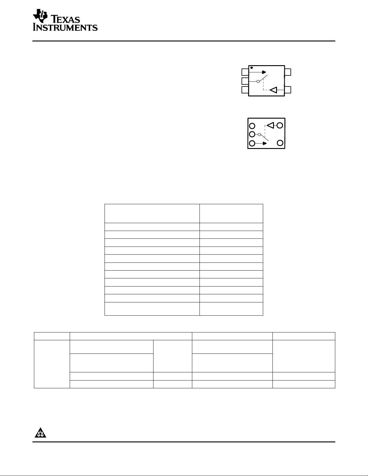
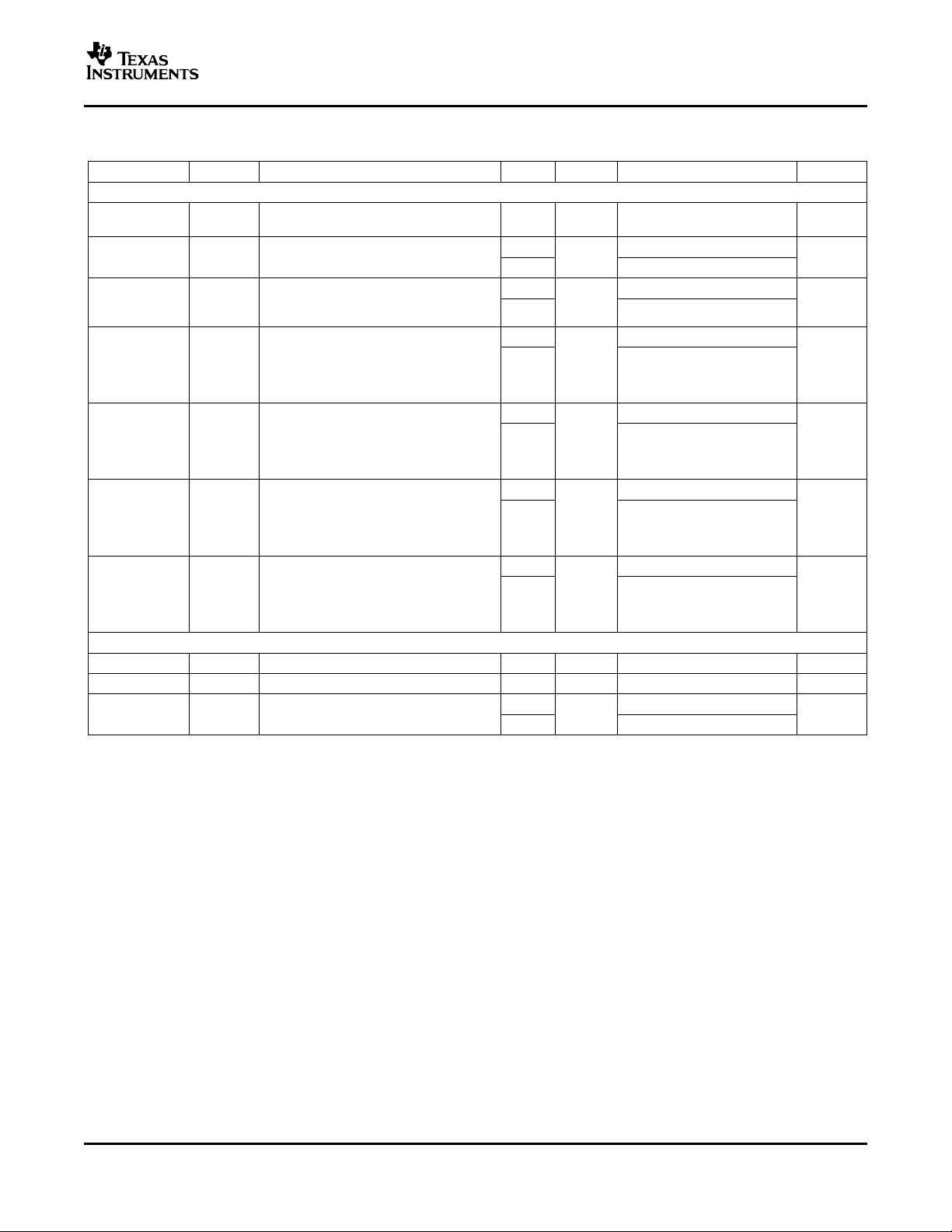
DBV OR DCK PACKAGE
(TOP VIEW)
1
2
3
5
4
NO
COM
GND
IN
V
+
YEP OR YZP PACKAGE
(BOTTOM VIEW)
3
2
1
4
5
NO
COM
GND
IN
V
+
TS5A1066
10- Ω SPST ANALOG SWITCH
SCDS185B – JANUARY 2005 – REVISED APRIL 2006
FEATURES
• Low ON-State Resistance (10 Ω )
• Control Inputs Are 5.5-V Tolerant
• Low Charge Injection
• Low Total Harmonic Distortion (THD)
• 1.65-V to 5.5-V Single-Supply Operation
• Latch-Up Performance Exceeds 100 mA Per
JESD 78, Class II
• ESD Performance Tested Per JESD 22
– 2000-V Human-Body Model
(A114-B, Class II)
– 1000-V Charged-Device Model (C101)
DESCRIPTION/ORDERING INFORMATION
The TS5A1066 is a single-pole single-throw (SPST) analog switch that is designed to operate from 1.65 V to
5.5 V. This device can handle both digital and analog signals, and signals up to V
either direction.
(peak) can be transmitted in
+
T
A
–40 ° C to 85 ° C
SUMMARY OF CHARACTERISTICS
Configuration Single-Throw Demultiplexer
Number of channels 1
ON-state resistance (ron) 7.5 Ω
ON-state resistance flatness (r
Turn-on/turn-off time (tON/t
Charge injection (Q
Bandwidth (BW) 400 MHz
OFF isolation (O
Total harmonic distortion (THD) 0.14%
Leakage current (I
Power-supply current (I+) 0.05 µ A
Package options
ISO
OFF
) 1 pC
C
) –68 dB at 10 MHz
COM(OFF)
) 2.5 Ω
on(flat)
) 9.5 ns/2 ns
Single-Pole,
(1 × SPST)
± 0.1 µ A
5-pin DSBGA, SOT-23,
or SC-70
ORDERING INFORMATION
PACKAGE
NanoStar™ – WCSP (DSBGA)
0.23-mm Large Bump - YEP
NanoFree™ – WCSP (DSBGA)
0.23-mm Large Bump – YZP TS5A1066YZPR
(Pb-free)
SOT (SOT-23) – DBV Tape and reel TS5A1066DBVR JAD_
SOT (SC-70) – DCK Tape and reel TS5A1066DCKR JD_
(1)
Tape and reel JD_
ORDERABLE PART NUMBER TOP-SIDE MARKING
TS5A1066YEPR
(2)
(1) Package drawings, standard packing quantities, thermal data, symbolization, and PCB design guidelines are available at
(2) DBV/DCK: The actual top-side marking has one additional character that designates the assembly/test site.
PRODUCTION DATA information is current as of publication date.
Products conform to specifications per the terms of the Texas
Instruments standard warranty. Production processing does not
necessarily include testing of all parameters.
www.ti.com/sc/package.
YEP/YZP: The actual top-side marking has three preceding characters to denote year, month, and sequence code, and one following
character to designate the assembly/test site. Pin 1 identifier indicates solder-bump composition (1 = SnPb, • = Pb-free).
Please be aware that an important notice concerning availability, standard warranty, and use in critical applications of Texas
Instruments semiconductor products and disclaimers thereto appears at the end of this data sheet.
Copyright © 2005–2006, Texas Instruments Incorporated
Page 2
www.ti.com
TS5A1066
10- Ω SPST ANALOG SWITCH
SCDS185B – JANUARY 2005 – REVISED APRIL 2006
FUNCTION TABLE
IN
L OFF
H ON
NO TO COM,
COM TO NO
Absolute Minimum and Maximum Rating
(1) (2)
over operating free-air temperature range (unless otherwise noted)
MIN MAX UNIT
V
Supply voltage range
+
V
NO
Analog voltage range
V
COM
I
Analog port diode current VNO, V
K
I
NO
On-state switch current VNO, V
I
COM
V
Digital input voltage range
I
I
Digital input clamp current VI< 0 –50 mA
IK
I
+
Continuous current through each V+or GND –100 100 mA
I
GND
θ
Package thermal impedance
JA
T
Storage temperature range –65 150 ° C
stg
(1) Stresses beyond those listed under "absolute maximum ratings" may cause permanent damage to the device. These are stress ratings
only, and functional operation of the device at these or any other conditions beyond those indicated under "recommended operating
conditions" is not implied. Exposure to absolute-maximum-rated conditions for extended periods may affect device reliability.
(2) The algebraic convention, whereby the most negative value is a minimum and the most positive value is a maximum.
(3) All voltages are with respect to ground, unless otherwise specified.
(4) The input and output voltage ratings may be exceeded if the input and output clamp-current ratings are observed.
(5) This value is limited to 5.5 V maximum.
(6) The package thermal impedance is calculated in accordance with JESD 51-7.
(3)
(3) (4) (5)
–0.5 6.5 V
–0.5 V++ 0.5 V
< 0 or V
COM
= 0 to V
COM
(3) (4)
, V
NO
+
> V
COM
+
–50 50 mA
–50 50 mA
–0.5 6.5 V
DBV package 206
(6)
DCK package 252 ° C/W
YEP/YZP package 132
2
Submit Documentation Feedback
Page 3
www.ti.com
10- Ω SPST ANALOG SWITCH
SCDS185B – JANUARY 2005 – REVISED APRIL 2006
Electrical Characteristics for 5-V Supply
V+= 4.5 V to 5.5 V, TA= –40 ° C to 85 ° C (unless otherwise noted)
PARAMETER SYMBOL TEST CONDITIONS T
Analog Switch
Analog signal
range
ON-state Switch ON,
resistance See Figure 13
ON-state 25 ° C 2.5 5
resistance r
flatness
NO V
OFF leakage I
current V
COM V
OFF leakage I
current V
NO V
ON leakage I
current V
COM V
ON leakage I
current V
Digital Control Input (IN)
Input logic high V
Input logic low V
Input leakage
current
(1) The algebraic convention is used in this data sheet; the most negative value is shown in the minimum column.
V
, V
COM
NO
r
on(flat)
0 ≤ V
on
I
0 ≤ V
I
V
NO(OFF)
or 5.5 V µ A
V
V
COM(OFF)
or 5.5 V µ A
V
V
NO(ON)
or 5.5 V µ A
V
V
COM(ON)
or 5.5 V µ A
V
IH
IL
IIH, I
VI= 5.5 V or 0 5.5 V µ A
IL
≤ V+, 25 ° C 7.5 10
NO
= –30 mA,
COM
≤ V+, Switch ON,
NO
= –30 mA, See Figure 13
COM
= 1 V, 25 ° C –0.2 0.1 0.2
NO
= 4.5 V,
COM
= 4.5 V,
NO
= 1 V,
COM
= 1 V, 25 ° C –0.1 0.05 0.1
COM
= 4.5 V,
NO
= 4.5 V,
COM
= 1 V,
NO
= 1 V, 25 ° C –0.2 0.1 0.2
NO
= Open,
COM
= 4.5 V,
NO
= Open,
COM
= 1 V, 25 ° C –0.1 0.05 0.1
COM
= Open,
NO
= 4.5 V,
COM
= Open,
NO
(1)
Switch OFF,
See Figure 14
Switch OFF,
See Figure 14
Switch ON,
See Figure 15
Switch ON,
See Figure 15
A
V
+
MIN TYP MAX UNIT
0 V
Full 12
Full 6
4.5 V Ω
4.5 V Ω
Full –2 2
Full –0.2 0.2
Full –2 2
Full –0.2 0.2
Full V+× 0.7 5.5 V
Full 0 V+× 0.3 V
25 ° C –0.1 0.05 0.1
Full –1 1
TS5A1066
V
+
Submit Documentation Feedback
3
Page 4
www.ti.com
TS5A1066
10- Ω SPST ANALOG SWITCH
SCDS185B – JANUARY 2005 – REVISED APRIL 2006
Electrical Characteristics for 5-V Supply (continued)
V+= 4.5 V to 5.5 V, TA= –40 ° C to 85 ° C (unless otherwise noted)
PARAMETER SYMBOL TEST CONDITIONS T
A
Dynamic
V
= 3 V, CL= 35 pF,
Turn-on time t
Turn-off time t
Charge V
injection CL= 0.1 nF,
ON
OFF
Q
C
NO
OFF C
capacitance
NO(OFF)
COM
OFF C
capacitance
COM(OFF)
NO
ON C
capacitance
NO(ON)
COM
ON C
capacitance
Digital input
capacitance
COM(ON)
C
Bandwidth BW See Figure 18 25 ° C 5 V 400 MHz
OFF isolation O
Total harmonic RL= 600 Ω , f = 20 Hz to 20 kHz,
distortion CL= 50 pF, See Figure 21
ISO
THD 25 ° C 5 V 0.14 %
COM
RL= 300 Ω , See Figure 17
V
= 3 V, CL= 35 pF,
COM
RL= 300 Ω , See Figure 17
= 0,
GEN
V
= V+or GND,
NO
Switch OFF,
V
= V+or GND,
COM
Switch OFF,
V
= V+or GND,
NO
Switch ON,
V
= V+or GND,
COM
Switch ON,
VI= V+or GND, See Figure 16 25 ° C 5 V 2.2 pF
I
See Figure 20 25 ° C 5 V 1 pC
See Figure 16 25 ° C 5 V 6.8 pF
See Figure 16 25 ° C 5 V 6.8 pF
See Figure 16 25 ° C 5 V 14 pF
See Figure 16 25 ° C 5 V 14 pF
RL= 50 Ω ,
Switch ON,
RL= 50 Ω , Switch OFF,
f = 10 MHz, See Figure 19
25 ° C 5 V 3.5 4.8 5.5
Full 4.5 V to 5.5 V 3.5 7.5
25 ° C 5 V 2 3 4.5
Full 4.5 V to 5.5 V 2 5.5
25 ° C 5 V –68 dB
Supply
Positive supply
current
I
VI= V+or GND, Switch ON or OFF 5.5 V µ A
+
25 ° C 0.05 1
Full 5
V
+
MIN TYP MAX UNIT
ns
ns
4
Submit Documentation Feedback
Page 5
www.ti.com
10- Ω SPST ANALOG SWITCH
SCDS185B – JANUARY 2005 – REVISED APRIL 2006
Electrical Characteristics for 3.3-V Supply
V+= 3 V to 3.6 V, TA= –40 ° C to 85 ° C (unless otherwise noted)
PARAMETER SYMBOL TEST CONDITIONS T
Analog Switch
Analog signal
range
ON-state Switch ON,
resistance See Figure 13
ON-state 25 ° C 5 10
resistance r
flatness
NO V
OFF leakage I
current V
COM V
OFF leakage I
current V
NO V
ON leakage I
current V
COM V
ON leakage I
current V
Digital Control Input (IN)
Input logic high V
Input logic low V
Input leakage
current
(1) The algebraic convention is used in this data sheet; the most negative value is shown in the minimum column.
V
, V
COM
NO
r
on
on(flat)
NO(OFF)
COM(OFF)
NO(ON)
COM(ON)
IH
IL
IIH, I
IL
0 ≤ V
I
0 ≤ V
I
≤ V+, 25 ° C 11.5 14
NO
= –24 mA,
COM
≤ V+, Switch ON,
NO
= –24 mA, See Figure 13
COM
V
= 1 V, 25 ° C –0.2 0.1 0.2
NO
= 3 V,
COM
or 3.6 V µ A
= 3 V,
NO
V
= 1 V,
COM
V
= 1 V, 25 ° C –0.1 0.05 0.1
COM
= 3 V,
NO
or 3.6 V µ A
= 3 V,
COM
V
= 1 V,
NO
V
= 1 V, 25 ° C –0.2 0.1 0.2
NO
= Open,
COM
or 3.6 V µ A
= 3 V,
NO
V
= Open,
COM
V
= 1 V, 25 ° C –0.1 0.05 0.1
COM
= Open,
NO
or 3.6 V µ A
= 3 V,
COM
V
= Open,
NO
Switch OFF,
See Figure 14
Switch OFF,
See Figure 14
Switch ON,
See Figure 15
Switch ON,
See Figure 15
VI= 5.5 V or 0 3.6 V µ A
(1)
A
V
+
MIN TYP MAX UNIT
0 V
Full 17
Full 12
3 V Ω
3 V Ω
Full –2 2
Full –0.2 0.2
Full –2 2
Full –0.2 0.2
Full V+× 0.7 5.5 V
Full 0 V+× 0.3 V
25 ° C –0.1 0.05 0.1
Full –1 1
TS5A1066
V
+
Submit Documentation Feedback
5
Page 6
www.ti.com
TS5A1066
10- Ω SPST ANALOG SWITCH
SCDS185B – JANUARY 2005 – REVISED APRIL 2006
Electrical Characteristics for 3.3-V Supply (continued)
V+= 3 V to 3.6 V, TA= –40 ° C to 85 ° C (unless otherwise noted)
PARAMETER SYMBOL TEST CONDITIONS T
A
Dynamic
V
= 2 V, CL= 35 pF,
Turn-on time t
Turn-off time t
Charge V
injection CL= 0.1 nF,
ON
OFF
Q
C
NO
OFF C
capacitance
NO(OFF)
COM V
OFF C
capacitance Switch OFF,
COM(OFF)
NO
ON C
capacitance
NO(ON)
COM V
ON C
capacitance Switch ON,
Digital input
capacitance
COM(ON)
C
Bandwidth BW See Figure 18 25 ° C 3.3 V 400 MHz
OFF isolation O
Total harmonic RL= 600 Ω , f = 20 Hz to 20 kHz,
distortion CL= 50 pF, See Figure 21
ISO
THD 25 ° C 3.3 V 0.2 %
COM
RL= 300 Ω , See Figure 17
V
= 2 V, CL= 35 pF,
COM
RL= 300 Ω , See Figure 17
= 0,
GEN
V
= V+or GND,
NO
Switch OFF,
= V+or
COM
GND, See Figure 16 25 ° C 3.3 V 6.8 pF
V
= V+or GND,
NO
Switch ON,
= V+or
COM
GND, See Figure 16 25 ° C 3.3 V 14 pF
VI= V+or GND, See Figure 16 25 ° C 3.3 V 2.2 pF
I
See Figure 20 25 ° C 3.3 V 1 pC
See Figure 16 25 ° C 3.3 V 6.8 pF
See Figure 16 25 ° C 3.3 V 14 pF
RL= 50 Ω ,
Switch ON,
RL= 50 Ω , Switch OFF,
f = 10 MHz, See Figure 19
25 ° C 3.3 V 4.5 5.5 8
Full 4.5 8.5
25 ° C 3.3 V 2 3 4.5
Full 2 5.5
25 ° C 3.3 V –68 dB
Supply
Positive supply
current
I
VI= V+or GND, Switch ON or OFF 3.6 V µ A
+
25 ° C 0.05 1
Full 5
V
+
MIN TYP MAX UNIT
3 V to
3.6 V
3 V to
3.6 V
ns
ns
6
Submit Documentation Feedback
Page 7

www.ti.com
10- Ω SPST ANALOG SWITCH
SCDS185B – JANUARY 2005 – REVISED APRIL 2006
Switch OFF,
See Figure 14
Switch OFF,
See Figure 14
Switch ON,
See Figure 15
Switch ON,
See Figure 15
(1)
A
V
+
MIN TYP MAX UNIT
0 V
Full 27
Full 20
2.3 V Ω
2.3 V Ω
Full –2 2
Full –0.2 0.2
Full –2 2
Full –0.2 0.2
Full V+× 0.7 5.5 V
Full 0 V+× 0.3 V
25 ° C –0.1 0.05 0.1
Full –1 1
Electrical Characteristics for 2.5-V Supply
V+= 2.3 V to 2.7 V, TA= –40 ° C to 85 ° C (unless otherwise noted)
PARAMETER SYMBOL TEST CONDITIONS T
Analog Switch
Analog signal
range
ON-state Switch ON,
resistance See Figure 13
ON-state 25 ° C 7.5 15
resistance r
flatness
NO V
OFF leakage I
current V
COM V
OFF leakage I
current V
NO V
ON leakage I
current V
COM V
ON leakage I
current V
Digital Control Input (IN)
Input logic high V
Input logic low V
Input leakage
current
(1) The algebraic convention is used in this data sheet; the most negative value is shown in the minimum column.
V
, V
COM
NO
r
on
on(flat)
NO(OFF)
COM(OFF)
NO(ON)
COM(ON)
IH
IL
IIH, I
IL
0 ≤ V
I
0 ≤ V
I
≤ V+, 25 ° C 20 24
NO
= –8 mA,
COM
≤ V+, Switch ON,
NO
= –8 mA, See Figure 13
COM
V
= 0.5 V, 25 ° C –0.2 0.1 0.2
NO
= 2.2 V,
COM
or 2.7 V µ A
= 2.2 V,
NO
V
= 0.5 V,
COM
V
= 0.5 V, 25 ° C –0.1 0.05 0.1
COM
= 2.2 V,
NO
or 2.7 V µ A
= 2.2 V,
COM
V
= 0.5 V,
NO
V
= 0.5 V, 25 ° C –0.2 0.1 0.2
NO
= Open,
COM
or 2.7 V µ A
= 2.2 V,
NO
V
= Open,
COM
V
= 0.5 V, 25 ° C –0.1 0.05 0.1
COM
= Open,
NO
or 2.7 V µ A
= 2.2 V,
COM
V
= Open,
NO
VI= 5.5 V or 0 2.7 V µ A
TS5A1066
V
+
Submit Documentation Feedback
7
Page 8
www.ti.com
TS5A1066
10- Ω SPST ANALOG SWITCH
SCDS185B – JANUARY 2005 – REVISED APRIL 2006
Electrical Characteristics for 2.5-V Supply (continued)
V+= 2.3 V to 2.7 V, TA= –40 ° C to 85 ° C (unless otherwise noted)
PARAMETER SYMBOL TEST CONDITIONS T
A
Dynamic
V
= 1.5 V, CL= 35 pF,
Turn-on time t
Turn-off time t
Charge V
injection CL= 0.1 nF,
ON
OFF
Q
C
NO
OFF C
capacitance
NO(OFF)
COM
OFF C
capacitance
COM(OFF)
NO
ON C
capacitance
NO(ON)
COM
ON C
capacitance
Digital input
capacitance
COM(ON)
C
I
Bandwidth BW See Figure 18 25 ° C 2.5 V 400 MHz
OFF isolation O
Total harmonic RL= 600 Ω , f = 20 Hz to 20 kHz,
distortion CL= 50 pF, See Figure 21
ISO
THD 25 ° C 2.5 V 0.32 %
COM
RL= 300 Ω , See Figure 17
V
= 1.5 V, CL= 35 pF,
COM
RL= 300 Ω , See Figure 17
= 0,
V
Switch OFF,
V
Switch OFF,
V
Switch ON,
V
Switch ON,
GEN
= V+or GND,
NO
= V+or GND,
COM
= V+or GND,
NO
= V+or GND,
COM
See Figure 20 25 ° C 2.5 V 1 pC
See Figure 16 25 ° C 2.5 V 6.8 pF
See Figure 16 25 ° C 2.5 V 6.8 pF
See Figure 16 25 ° C 2.5 V 14 pF
See Figure 16 25 ° C 2.5 V 14 pF
VI= V+or GND, See Figure 16 25 ° C 2.5 V 2.2 pF
RL= 50 Ω ,
Switch ON,
RL= 50 Ω , Switch OFF,
f = 10 MHz, See Figure 19
25 ° C 2.5 V 4.5 5.5 8
Full 4.5 8.5
25 ° C 2.5 V 1.5 2.5 4
Full 1.5 5.5
25 ° C 2.5 V –68 dB
Supply
Positive supply
current
I
VI= V+or GND, Switch ON or OFF 2.7 V µ A
+
25 ° C 0.05 1
Full 5
2.3 V to
2.7 V
2.3 V to
2.7 V
V
+
MIN TYP MAX UNIT
ns
ns
8
Submit Documentation Feedback
Page 9
www.ti.com
10- Ω SPST ANALOG SWITCH
SCDS185B – JANUARY 2005 – REVISED APRIL 2006
Electrical Characteristics for 1.8-V Supply
V+= 1.65 V to 1.95 V, TA= –40 ° C to 85 ° C (unless otherwise noted)
PARAMETER SYMBOL TEST CONDITIONS T
Analog Switch
Analog signal
range
ON-state Switch ON,
resistance See Figure 13
ON-state 25 ° C 64.5 70
resistance r
flatness
NO V
OFF leakage I
current V
COM V
OFF leakage I
current V
NO V
ON leakage I
current V
COM V
ON leakage I
current V
Digital Control Input (IN)
Input logic high V
Input logic low V
Input leakage
current
(1) The algebraic convention is used in this data sheet; the most negative value is shown in the minimum column.
V
, V
COM
NO
r
on(flat)
0 ≤ V
on
I
0 ≤ V
I
V
NO(OFF)
or 1.95 V µ A
V
V
COM(OFF)
or 1.95 V µ A
V
V
NO(ON)
or 1.95 V µ A
V
V
COM(ON)
or 1.95 V µ A
V
IH
IL
IIH, I
VI= 5.5 V or 0 1.95 V µ A
IL
≤ V+, 25 ° C 74.5 80
NO
= –4 mA,
COM
≤ V+, Switch ON,
NO
= –4 mA, See Figure 13
COM
= 0.3 V, 25 ° C –0.2 0.1 0.2
NO
= 1.65 V,
COM
= 1.65 V,
NO
= 0.3 V,
COM
= 0.3 V, 25 ° C –0.1 0.05 0.1
COM
= 1.65 V,
NO
= 1.65 V,
COM
= 0.3 V,
NO
= 0.3 V, 25 ° C –0.2 0.1 0.2
NO
= Open,
COM
= 1.65 V,
NO
= Open,
COM
= 0.3 V, 25 ° C –0.1 0.05 0.1
COM
= Open,
NO
= 1.65 V,
COM
= Open,
NO
(1)
Switch OFF,
See Figure 14
Switch OFF,
See Figure 14
Switch ON,
See Figure 15
Switch ON,
See Figure 15
A
V
+
MIN TYP MAX UNIT
0 V
Full 100
Full 90
1.65 V Ω
1.65 V Ω
Full –2 2
Full –0.2 0.2
Full –2 2
Full –0.2 0.2
Full V+× 0.65 5.5 V
Full 0 V+× 0.35 V
25 ° C –0.1 0.05 0.1
Full –1 1
TS5A1066
V
+
Submit Documentation Feedback
9
Page 10

www.ti.com
TS5A1066
10- Ω SPST ANALOG SWITCH
SCDS185B – JANUARY 2005 – REVISED APRIL 2006
Electrical Characteristics for 1.8-V Supply (continued)
V+= 1.65 V to 1.95 V, TA= –40 ° C to 85 ° C (unless otherwise noted)
PARAMETER SYMBOL TEST CONDITIONS T
A
Dynamic
V
= 1.3 V, CL= 35 pF,
Turn-on time t
Turn-off time t
Charge V
injection CL= 0.1 nF,
ON
OFF
Q
C
NO
OFF C
capacitance
NO(OFF)
COM
OFF C
capacitance
COM(OFF)
NO
ON C
capacitance
NO(ON)
COM
ON C
capacitance
Digital input
capacitance
COM(ON)
C
Bandwidth BW See Figure 18 25 ° C 1.8 V 400 MHz
OFF isolation O
Total harmonic RL= 600 Ω , f = 20 Hz to 20 kHz,
distortion CL= 50 pF, See Figure 21
ISO
THD 25 ° C 1.8 V 0.32 %
COM
RL= 300 Ω , See Figure 17
V
= 1.3 V, CL= 35 pF,
COM
RL= 300 Ω , See Figure 17
= 0,
GEN
V
= V+or GND,
NO
Switch OFF,
V
= V+or GND,
COM
Switch OFF,
V
= V+or GND,
NO
Switch ON,
V
= V+or GND,
COM
Switch ON,
VI= V+or GND, See Figure 16 25 ° C 1.8 V 2.2 pF
I
See Figure 20 25 ° C 1.8 V 1 pC
See Figure 16 25 ° C 1.8 V 6.8 pF
See Figure 16 25 ° C 1.8 V 6.8 pF
See Figure 16 25 ° C 1.8 V 14 pF
See Figure 16 25 ° C 1.8 V 14 pF
RL= 50 Ω ,
Switch ON,
RL= 50 Ω , Switch OFF,
f = 10 MHz, See Figure 19
25 ° C 1.8 V 9.5 10 12
Full 8.5 13
25 ° C 1.8 V 1.5 2 4
Full 1.5 5.5
25 ° C 1.8 V –68 dB
Supply
Positive supply
current
I
VI= V+or GND, Switch ON or OFF 1.95 V µ A
+
25 ° C 0.05 1
Full 5
1.65 V to
1.95 V
1.65 V to
1.95 V
V
+
MIN TYP MAX UNIT
ns
ns
10
Submit Documentation Feedback
Page 11

www.ti.com
0
10
20
30
40
50
60
70
80
90
0 1 2 3 4 5
VCC = 1.65 V
V
COM
(V)
r
on
VCC = 2.3 V
VCC = 3 V
VCC = 4.5 V
0
1
2
3
4
5
6
7
8
9
V+ = 4.5 V
85C
25C
–40C
V
COM
(V)
r
on
()
0 0.5 1 1.5 2 2.5 3 3.5 4 4.5 5
0
2
4
6
8
10
12
14
V
COM
V
r
on
(
V+ = 3 V
85C
25C
–40C
0 0.5 1 1.5 2 2.5 3 3.5
TS5A1066
10- Ω SPST ANALOG SWITCH
SCDS185B – JANUARY 2005 – REVISED APRIL 2006
TYPICAL PERFORMANCE
Figure 1. ronvs V
Figure 2. ronvs V
COM
(V
COM
= 3 V)
+
Figure 3. ronvs V
Submit Documentation Feedback
(V
COM
= 5 V)
+
11
Page 12

www.ti.com
TA (C)
Leakage (nA)
−1
0
1
2
3
4
5
−60 −40 −20 0 20 40 60 80 100
I
COM(ON)
COM NO
I
NO(ON)
NO COM
I
COM (OFF)
NO LO
I
COM (OFF)
NO HI
I
NO (OFF)
COM LO
I
NO (OFF)
COM HI
I
IN_VIN
‘IN’ C-LO
I
IN_VIN
‘IN’ C-HI
Bias Voltage (V)
Charge Injection (pC)
3.5
3
2.5
2
1.5
1
0.5
0
0 0.5 1 1.5 2 2.5 3 3.5
V+ (V)
0
2
4
6
8
10
12
0 1 2 3 4 5 6
t
ON
/t
OFF
(ns)
T
A
= 25°C
t
ON
t
OFF
TS5A1066
10- Ω SPST ANALOG SWITCH
SCDS185B – JANUARY 2005 – REVISED APRIL 2006
TYPICAL PERFORMANCE
Figure 4. Leakage Current vs Temperature (V
Figure 5. Charge Injection (Q
) vs Bias Voltage
C
+
= 5.5 V)
12
Figure 6. t
and t
ON
Submit Documentation Feedback
vs Supply Voltage
OFF
Page 13

www.ti.com
0
1
2
3
4
5
6
−40 25 85
t
ON
/t
OFF
(ns)
TA (C)
t
OFF
t
ON
0.0
0.5
1.0
1.5
2.0
2.5
3.0
3.5
0 1 2 3 4 5 6
V+ (V)
Logic Level Threshold (nA)
V
IH
V
IL
Frequency (MHz)
Gain (dB)
−4.5
−4
−3.5
−3
−2.5
−2
−1.5
−1
−0.5
0
100 1K 10K 100K 1M
TS5A1066
10- Ω SPST ANALOG SWITCH
SCDS185B – JANUARY 2005 – REVISED APRIL 2006
TYPICAL PERFORMANCE
Figure 7. t
and t
ON
vs Temperature (V
OFF
Figure 8. Logic-Level Threshold vs V
= 5 V)
+
+
Figure 9. Bandwidth (V
Submit Documentation Feedback
= 5 V)
+
13
Page 14

www.ti.com
−120
−100
−80
−60
−40
−20
0
100
1K
10K 100K
1M
Frequency (MHz)
Attenuation (dB)
Frequency (Hz)
THD + Noise (%)
0
0.05
0.1
0.15
0.2
0.25
0.3
0.35
0.4
10 100 1M 10M 100M
V+ = 3.3 V
V+ = 5 V
TA (C)
I
+
(nA)
0
100
200
300
400
500
600
700
−60 −40 −20 0 20 40 60 80 100
V+ = 5.5 V
TS5A1066
10- Ω SPST ANALOG SWITCH
SCDS185B – JANUARY 2005 – REVISED APRIL 2006
TYPICAL PERFORMANCE
Figure 10. OFF Isolation (V
Figure 11. Total Harmonic Distortion vs Frequency
= 5 V)
+
14
Figure 12. Power-Supply Current vs Temperature (V
Submit Documentation Feedback
= 5 V)
+
Page 15

www.ti.com
10- Ω SPST ANALOG SWITCH
SCDS185B – JANUARY 2005 – REVISED APRIL 2006
PIN DESCRIPTION
PIN NAME DESCRIPTION
1 NO Normally open
2 COM Common
3 GND Digital ground
4 IN Digital control to connect COM to NO
5 V
SYMBOL DESCRIPTION
V
COM
V
NO
r
on
r
on(flat)
I
NO(OFF)
I
NO(ON)
I
COM(OFF)
I
COM(ON)
V
IH
V
IL
V
I
IIH, I
t
ON
t
OFF
Voltage at COM
Voltage at NO
Resistance between COM and NO ports when the channel is ON
Difference between the maximum and minimum value of ron in a channel over the specified range of conditions
Leakage current measured at the NO port, with the corresponding channel (NO to COM) in the OFF state
Leakage current measured at the NO port, with the corresponding channel (NO to COM) in the ON state and the output
(COM) open
Leakage current measured at the COM port, with the corresponding channel (COM to NO) in the OFF state
Leakage current measured at the COM port, with the corresponding channel (COM to NO) in the ON state and the output
(NO) open
Minimum input voltage for logic high for the control input (IN)
Maximum input voltage for logic low for the control input (IN)
Voltage at the control input (IN)
Leakage current measured at the control input (IN)
IL
Turn-on time for the switch. This parameter is measured under the specified range of conditions and by the propagation
delay between the digital control (IN) signal and analog output (COM or NO) signal when the switch is turning ON.
Turn-off time for the switch. This parameter is measured under the specified range of conditions and by the propagation
delay between the digital control (IN) signal and analog output (COM or NO) signal when the switch is turning OFF.
Charge injection is a measurement of unwanted signal coupling from the control (IN) input to the analog (NO or COM)
Q
C
C
NO(OFF)
C
NO(ON)
C
COM(OFF)
C
COM(ON)
C
I
O
ISO
output. This is measured in coulomb (C) and measured by the total charge induced due to switching of the control
input.Charge injection, QC= CL× ∆ V
Capacitance at the NO port when the corresponding channel (NO to COM) is OFF
Capacitance at the NO port when the corresponding channel (NO to COM) is ON
Capacitance at the COM port when the corresponding channel (COM to NO) is OFF
Capacitance at the COM port when the corresponding channel (COM to NO) is ON
Capacitance of IN
OFF isolation of the switch is a measurement of OFF-state switch impedance. This is measured in dB in a specific
frequency, with the corresponding channel (NO to COM) in the OFF state.
BW Bandwidth of the switch. This is the frequency in which the gain of an ON channel is -3 dB below the DC gain.
THD
I
+
∆ I
+
Total harmonic distortion is defined as the ratio of the root mean square (RMS) value of the second, third, and higher
harmonics to the magnitude of fundamental harmonic.
Static power-supply current with the control (IN) pin at V+or GND
This is the increase in I+for each control (IN) input that is at the specified voltage, rather than at V+or GND.
Power supply
+
PARAMETER DESCRIPTION
, CLis the load capacitance and ∆ V
COM
is the change in analog output voltage.
COM
TS5A1066
Submit Documentation Feedback
15
Page 16

www.ti.com
V
+
I
COM
r
on
V
COM
V
NO
I
COM
GND
Channel ON
NO
V
I
COM
V
COM
V
I
= V
IH
or V
IL
V
NO
IN
+
+
Channel OFF
OFF-State Leakage Current
V
I
= V
IH
or V
IL
V
+
GND
NO
V
I
COM V
COM
V
NO
IN
+
+
+
Channel ON
ON-State Leakage Current
V
I
= V
IH
or V
IL
V
+
GND
NO
V
I
COM
V
COM
V
NO
IN
+
+
TS5A1066
10- Ω SPST ANALOG SWITCH
SCDS185B – JANUARY 2005 – REVISED APRIL 2006
PARAMETER MEASUREMENT INFORMATION
Figure 13. ON-State Resistance (r
Figure 14. OFF-State Leakage Current (I
)
on
COM(OFF)
, I
)
NO(OFF)
16
Figure 15. ON-State Leakage Current (I
Submit Documentation Feedback
, I
NO(ON)
COM(ON)
)
Page 17

www.ti.com
V
+
GND
IN
V
BIAS
V
I
VI = VIH or V
IL
V
BIAS
= V+ or GND
Capacitance is measured at NO,
COM, and IN inputs during ON
and OFF conditions.
Capacitance
Meter
V
NO
V
COM
NO
COM
C
L
(2)
R
L
V
COM
(3)
V
+
GND
NO
IN
V
NO
V
I
COM
Logic
Input
(1)
300 Ω
R
L
C
L
35 pFt
ON
TEST
300 Ω 35 pFt
OFF
50%
t
ON
t
OFF
50%
90% 90%
Logic
Input
(VI)
V
+
Switch
Output
(VNO)
0
(1) All input pulses are supplied by generators having the following characteristics: PRR ≤ 10 MHz, ZO = 50 , tr < 5 ns, tf < 5 ns.
(2) CL includes probe and jig capacitance.
(3) See Electrical Characteristics for V
COM
.
PARAMETER MEASUREMENT INFORMATION (continued)
TS5A1066
10- Ω SPST ANALOG SWITCH
SCDS185B – JANUARY 2005 – REVISED APRIL 2006
Figure 16. Capacitance (C
Figure 17. Turn-On (t
, C
I
COM(OFF)
ON
, C
) and Turn-Off Time (t
COM(ON)
, C
NO(OFF)
, C
)
OFF
)
NO(ON)
Submit Documentation Feedback
17
Page 18

www.ti.com
V
+
GND
NO
IN
V
I
COM
50
50
V
NO
V
COM
Channel ON: NO to COM
Network Analyzer Setup
Source Power = 0 dBM
(632-mV P-P at 50- load)
DC Bias = 350 mV
Network Analyzer
Source
Signal
+
VI = VIH or V
IL
NO
COM
V
NO
V
COM
Channel OFF: NO to COM
Network Analyzer Setup
Source Power = 0 dBM
(632-mV P-P at 50- load)
DC Bias = 350 mV
50
V
+
GND
50
50
Network Analyzer
Source
Signal
IN
V
I
+
VI = VIH or V
IL
TS5A1066
10- Ω SPST ANALOG SWITCH
SCDS185B – JANUARY 2005 – REVISED APRIL 2006
PARAMETER MEASUREMENT INFORMATION (continued)
Figure 18. Bandwidth (BW)
18
Figure 19. OFF Isolation (O
Submit Documentation Feedback
)
ISO
Page 19

www.ti.com
V
+
GND
NO
IN
R
GEN
V
I
COM V
COM
C
L
(2)
OFF
V
COM
ON OFF
∆V
COM
V
GEN
+
V
I
= VIH or V
IL
C
L
= 0.1 nF
V
GEN
= 0 to V
+
R
GEN
= 0
Q
C
= C
L
× ∆V
COM
Logic
Input
(1)
V
IH
V
IL
Logic
Input
(V
I)
(1) All input pulses are supplied by generators having the following characteristics: PRR ≤ 10 MHz, ZO = 50 , tr < 5 ns, tf < 5 ns.
(2) CL includes probe and jig capacitance.
V
+
GND
NO
COM
10 F
R
L
C
L
(1)
R
L
= 600 Ω
C
L
= 50 pF
V
SOURCE
= V
+
P-P
f
SOURCE
= 20 Hz to 20 kHz
R
L
V
SOURCE
V+/2
Analyzer
10 F
Channel ON: COM to NO
V
O
IN
V
I
+
V
I
= V
IH
or V
IL
(1) CL includes probe and jig capacitance.
PARAMETER MEASUREMENT INFORMATION (continued)
TS5A1066
10- Ω SPST ANALOG SWITCH
SCDS185B – JANUARY 2005 – REVISED APRIL 2006
Figure 20. Charge Injection (Q
)
C
Figure 21. Total Harmonic Distortion (THD)
Submit Documentation Feedback
19
Page 20

PACKAGE OPTION ADDENDUM
www.ti.com
29-May-2007
PACKAGING INFORMATION
Orderable Device Status
(1)
Package
Type
Package
Drawing
Pins Package
Qty
Eco Plan
TS5A1066DBVR ACTIVE SOT-23 DBV 5 3000 Green (RoHS &
no Sb/Br)
TS5A1066DBVRE4 ACTIVE SOT-23 DBV 5 3000 Green (RoHS &
no Sb/Br)
TS5A1066DBVRG4 ACTIVE SOT-23 DBV 5 3000 Green (RoHS &
no Sb/Br)
TS5A1066DCKR ACTIVE SC70 DCK 5 3000 Green (RoHS &
no Sb/Br)
TS5A1066DCKRE4 ACTIVE SC70 DCK 5 3000 Green (RoHS &
no Sb/Br)
TS5A1066DCKRG4 ACTIVE SC70 DCK 5 3000 Green (RoHS &
no Sb/Br)
TS5A1066YZPR ACTIVE WCSP YZP 5 3000 Green (RoHS &
no Sb/Br)
(1)
The marketing status values are defined as follows:
ACTIVE: Product device recommended for new designs.
LIFEBUY: TI has announced that the device will be discontinued, and a lifetime-buy period is in effect.
NRND: Not recommended for new designs. Device is in production to support existing customers, but TI does not recommend using this part in
a new design.
PREVIEW: Device has been announced but is not in production. Samples may or may not be available.
OBSOLETE: TI has discontinued the production of the device.
(2)
Lead/Ball Finish MSL Peak Temp
CU NIPDAU Level-1-260C-UNLIM
CU NIPDAU Level-1-260C-UNLIM
CU NIPDAU Level-1-260C-UNLIM
CU NIPDAU Level-1-260C-UNLIM
CU NIPDAU Level-1-260C-UNLIM
CU NIPDAU Level-1-260C-UNLIM
SNAGCU Level-1-260C-UNLIM
(3)
(2)
Eco Plan - The planned eco-friendly classification: Pb-Free (RoHS), Pb-Free (RoHS Exempt), or Green (RoHS & no Sb/Br) - please check
http://www.ti.com/productcontent for the latest availability information and additional product content details.
TBD: The Pb-Free/Green conversion plan has not been defined.
Pb-Free (RoHS): TI's terms "Lead-Free" or "Pb-Free" mean semiconductor products that are compatible with the current RoHS requirements
for all 6 substances, including the requirement that lead not exceed 0.1% by weight in homogeneous materials. Where designed to be soldered
at high temperatures, TI Pb-Free products are suitable for use in specified lead-free processes.
Pb-Free (RoHS Exempt): This component has a RoHS exemption for either 1) lead-based flip-chip solder bumps used between the die and
package, or 2) lead-based die adhesive used between the die and leadframe. The component is otherwise considered Pb-Free (RoHS
compatible) as defined above.
Green (RoHS & no Sb/Br): TI defines "Green" to mean Pb-Free (RoHS compatible), and free of Bromine (Br) and Antimony (Sb) based flame
retardants (Br or Sb do not exceed 0.1% by weight in homogeneous material)
(3)
MSL, Peak Temp. -- The Moisture Sensitivity Level rating according to the JEDEC industry standard classifications, and peak solder
temperature.
Important Information and Disclaimer:The information provided on this page represents TI's knowledge and belief as of the date that it is
provided. TI bases its knowledge and belief on information provided by third parties, and makes no representation or warranty as to the
accuracy of such information. Efforts are underway to better integrate information from third parties. TI has taken and continues to take
reasonable steps to provide representative and accurate information but may not have conducted destructive testing or chemical analysis on
incoming materials and chemicals. TI and TI suppliers consider certain information to be proprietary, and thus CAS numbers and other limited
information may not be available for release.
In no event shall TI's liability arising out of such information exceed the total purchase price of the TI part(s) at issue in this document sold by TI
to Customer on an annual basis.
Addendum-Page 1
Page 21

PACKAGE MATERIALS INFORMATION
www.ti.com
TAPE AND REEL INFORMATION
11-Mar-2008
*All dimensions are nominal
Device Package
Type
TS5A1066DBVR SOT-23 DBV 5 3000 180.0 9.2 3.23 3.17 1.37 4.0 8.0 Q3
TS5A1066DCKR SC70 DCK 5 3000 180.0 9.2 2.24 2.34 1.22 4.0 8.0 Q3
Package
Drawing
Pins SPQ Reel
Diameter
(mm)
Reel
Width
W1 (mm)
A0 (mm) B0 (mm) K0 (mm) P1
(mm)W(mm)
Pin1
Quadrant
Pack Materials-Page 1
Page 22

PACKAGE MATERIALS INFORMATION
www.ti.com
11-Mar-2008
*All dimensions are nominal
Device Package Type Package Drawing Pins SPQ Length (mm) Width (mm) Height (mm)
TS5A1066DBVR SOT-23 DBV 5 3000 202.0 201.0 28.0
TS5A1066DCKR SC70 DCK 5 3000 202.0 201.0 28.0
Pack Materials-Page 2
Page 23

Page 24

Page 25

Page 26

IMPORTANT NOTICE
Texas Instruments Incorporated and its subsidiaries (TI) reserve the right to make corrections, modifications, enhancements, improvements,
and other changes to its products and services at any time and to discontinue any product or service without notice. Customers should
obtain the latest relevant information before placing orders and should verify that such information is current and complete. All products are
sold subject to TI’s terms and conditions of sale supplied at the time of order acknowledgment.
TI warrants performance of its hardware products to the specifications applicable at the time of sale in accordance with TI’s standard
warranty. Testing and other quality control techniques are used to the extent TI deems necessary to support this warranty. Except where
mandated by government requirements, testing of all parameters of each product is not necessarily performed.
TI assumes no liability for applications assistance or customer product design. Customers are responsible for their products and
applications using TI components. To minimize the risks associated with customer products and applications, customers should provide
adequate design and operating safeguards.
TI does not warrant or represent that any license, either express or implied, is granted under any TI patent right, copyright, mask work right,
or other TI intellectual property right relating to any combination, machine, or process in which TI products or services are used. Information
published by TI regarding third-party products or services does not constitute a license from TI to use such products or services or a
warranty or endorsement thereof. Use of such information may require a license from a third party under the patents or other intellectual
property of the third party, or a license from TI under the patents or other intellectual property of TI.
Reproduction of TI information in TI data books or data sheets is permissible only if reproduction is without alteration and is accompanied
by all associated warranties, conditions, limitations, and notices. Reproduction of this information with alteration is an unfair and deceptive
business practice. TI is not responsible or liable for such altered documentation. Information of third parties may be subject to additional
restrictions.
Resale of TI products or services with statements different from or beyond the parameters stated by TI for that product or service voids all
express and any implied warranties for the associated TI product or service and is an unfair and deceptive business practice. TI is not
responsible or liable for any such statements.
TI products are not authorized for use in safety-critical applications (such as life support) where a failure of the TI product would reasonably
be expected to cause severe personal injury or death, unless officers of the parties have executed an agreement specifically governing
such use. Buyers represent that they have all necessary expertise in the safety and regulatory ramifications of their applications, and
acknowledge and agree that they are solely responsible for all legal, regulatory and safety-related requirements concerning their products
and any use of TI products in such safety-critical applications, notwithstanding any applications-related information or support that may be
provided by TI. Further, Buyers must fully indemnify TI and its representatives against any damages arising out of the use of TI products in
such safety-critical applications.
TI products are neither designed nor intended for use in military/aerospace applications or environments unless the TI products are
specifically designated by TI as military-grade or "enhanced plastic." Only products designated by TI as military-grade meet military
specifications. Buyers acknowledge and agree that any such use of TI products which TI has not designated as military-grade is solely at
the Buyer's risk, and that they are solely responsible for compliance with all legal and regulatory requirements in connection with such use.
TI products are neither designed nor intended for use in automotive applications or environments unless the specific TI products are
designated by TI as compliant with ISO/TS 16949 requirements. Buyers acknowledge and agree that, if they use any non-designated
products in automotive applications, TI will not be responsible for any failure to meet such requirements.
Following are URLs where you can obtain information on other Texas Instruments products and application solutions:
Products Applications
Amplifiers amplifier.ti.com Audio www.ti.com/audio
Data Converters dataconverter.ti.com Automotive www.ti.com/automotive
DSP dsp.ti.com Broadband www.ti.com/broadband
Clocks and Timers www.ti.com/clocks Digital Control www.ti.com/digitalcontrol
Interface interface.ti.com Medical www.ti.com/medical
Logic logic.ti.com Military www.ti.com/military
Power Mgmt power.ti.com Optical Networking www.ti.com/opticalnetwork
Microcontrollers microcontroller.ti.com Security www.ti.com/security
RFID www.ti-rfid.com Telephony www.ti.com/telephony
RF/IF and ZigBee® Solutions www.ti.com/lprf Video & Imaging www.ti.com/video
Mailing Address: Texas Instruments, Post Office Box 655303, Dallas, Texas 75265
Copyright © 2008, Texas Instruments Incorporated
Wireless www.ti.com/wireless
Page 27

 Loading...