

Page 1

TS4999
Filter-free stereo 2.8 W class D audio power amplifier
with selectable 3D sound effects
Features
■ Operates from V
■ Dedicated standby mode active low/channel
■ Output power per channel: 2.8 W at 5 V into
4 Ω with 10% THD+N or 0.7 W at 3.6 V into 8 Ω
with 1% THD+N max.
■ Selectable 3D sound effect
■ Four gain setting steps: 3.5, 6, 9.5 and 12 dB
■ Low current consumption
■ PSSR: 63 dB typical at 217 Hz.
■ Fast start up phase: 7.8 ms
■ Short-circuit and thermal shutdown protection
■ Flip chip 18-bump lead-free package
= 2.4 to 5.5 V
CC
Applications
■ Cellular phones
■ PDAs
■ Notebook PCs
Flip chip 18-bump package
Pin connections (top view)
LOUT-
LOUT-
LOUT+
LOUT+
STDBYL
STDBYL
LPVCC
LPVCC
AGND
AGND
LIN- RIN-
LIN- RIN-
PGND
PGND
G1
G1
G0
G0
RPVCC
RPVCC
AVCC
AVCC
ROUT-
ROUT-
ROUT+
ROUT+
STDBYR
STDBYR
RIN+3D
Description
LIN+
LIN+
RIN+3D
The TS4999 is a stereo fully-differential class D
power amplifier. It can drive up to 1.35 W into a
8 Ω load at 5 V per channel. The device has four
different gain settings utilizing two discrete pins,
G0 and G1.
Pop and click reduction circuitry provides low
on/off switch noise while allowing the device to
start within 8 ms. 3D enhancement effects are
selected through one digital input pin that allows
more amazing stereo audio sound.
Two standby pins (active low) allow each channel
to be switched off separately.
The TS4999 is available in a flip chip, 18-bump,
lead-free package.
December 2008 Rev 1 1/36
www.st.com
36
Page 2

Contents TS4999
Contents
1 Absolute maximum ratings . . . . . . . . . . . . . . . . . . . . . . . . . . . . . . . . . . . 3
2 Application information . . . . . . . . . . . . . . . . . . . . . . . . . . . . . . . . . . . . . . 5
3 Electrical characteristics . . . . . . . . . . . . . . . . . . . . . . . . . . . . . . . . . . . . . 7
3.1 Electrical characteristic curves . . . . . . . . . . . . . . . . . . . . . . . . . . . . . . . . . 13
4 Application information . . . . . . . . . . . . . . . . . . . . . . . . . . . . . . . . . . . . . 24
4.1 Differential configuration principle . . . . . . . . . . . . . . . . . . . . . . . . . . . . . . 24
4.2 Gain settings . . . . . . . . . . . . . . . . . . . . . . . . . . . . . . . . . . . . . . . . . . . . . . 24
4.3 3D effect enhancement . . . . . . . . . . . . . . . . . . . . . . . . . . . . . . . . . . . . . . 24
4.4 Low frequency response . . . . . . . . . . . . . . . . . . . . . . . . . . . . . . . . . . . . . 25
4.5 Circuit decoupling . . . . . . . . . . . . . . . . . . . . . . . . . . . . . . . . . . . . . . . . . . . 26
4.6 Wakeup (t
4.7 Consumption in shutdown mode . . . . . . . . . . . . . . . . . . . . . . . . . . . . . . . 28
4.8 Single-ended input configuration . . . . . . . . . . . . . . . . . . . . . . . . . . . . . . . 28
4.9 Output filter considerations . . . . . . . . . . . . . . . . . . . . . . . . . . . . . . . . . . . . 29
4.10 Short-circuit protection . . . . . . . . . . . . . . . . . . . . . . . . . . . . . . . . . . . . . . . 30
4.11 Thermal shutdown . . . . . . . . . . . . . . . . . . . . . . . . . . . . . . . . . . . . . . . . . . 30
) and shutdown (t
WU
) times . . . . . . . . . . . . . . . . . . . . . . . 26
STBY
5 Package mechanical data . . . . . . . . . . . . . . . . . . . . . . . . . . . . . . . . . . . . 31
5.1 Flip chip package . . . . . . . . . . . . . . . . . . . . . . . . . . . . . . . . . . . . . . . . . . . 31
5.2 Tape and reel package . . . . . . . . . . . . . . . . . . . . . . . . . . . . . . . . . . . . . . . 33
6 Ordering information . . . . . . . . . . . . . . . . . . . . . . . . . . . . . . . . . . . . . . . 34
7 Revision history . . . . . . . . . . . . . . . . . . . . . . . . . . . . . . . . . . . . . . . . . . . 35
2/36
Page 3
TS4999 Absolute maximum ratings
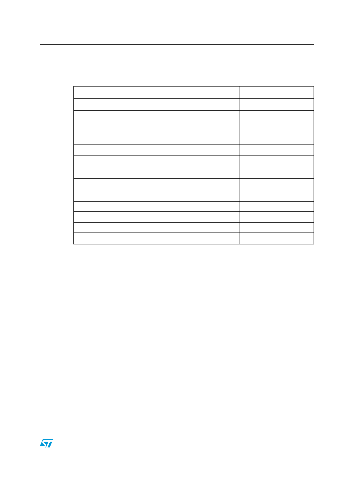
1 Absolute maximum ratings
Table 1. Key parameters and their absolute maximum ratings
Symbol Parameter Value Unit
(2)
(1)
(6)
(5)
(3)
6V
GND to V
CC
200 °C/W
Internally Limited
2kV
200 V
(4)
V
T
T
R
V
oper
Supply voltage
CC
Input voltage
in
Operating free air temperature range -40 to + 85 °C
Storage temperature -65 to +150 °C
stg
T
Maximum junction temperature 150 °C
j
Thermal resistance junction to ambient
thja
Pd Power dissipation
ESD
ESD
HBM: human body model
MM: machine model
Latch-up Latch-up immunity 200 mA
V
STBY
Standby pin voltage maximum voltage
GND to V
CC
Lead temperature (soldering, 10 secs) 260 °C
Output short-circuit protection
1. All voltages values are measured with respect to the ground pin.
2. The magnitude of input signal must never exceed VCC + 0.3 V / GND - 0.3 V
3. Device is protected in case of over temperature by a thermal shutdown active at 150° C.
4. Exceeding the power derating curves during a long period, involves abnormal operating condition.
5. Human body model: 100 pF discharged through a 1.5 kΩ resistor between two pins of the device, done for
all couples of pin combinations with other pins floating.
6. Machine model: a 200 pF capacitor is charged to the specified voltage, then discharged directly between
two pins of the device with no external series resistor (internal resistor < 5 Ω), done for all couples of pin
combinations with other pins floating.
7. Implemented short-circuit protection protects the amplifier against damage by short-circuit between
positive and negative outputs of each channel and between outputs and ground.
(7)
V
V
3/36
Page 4
Absolute maximum ratings TS4999
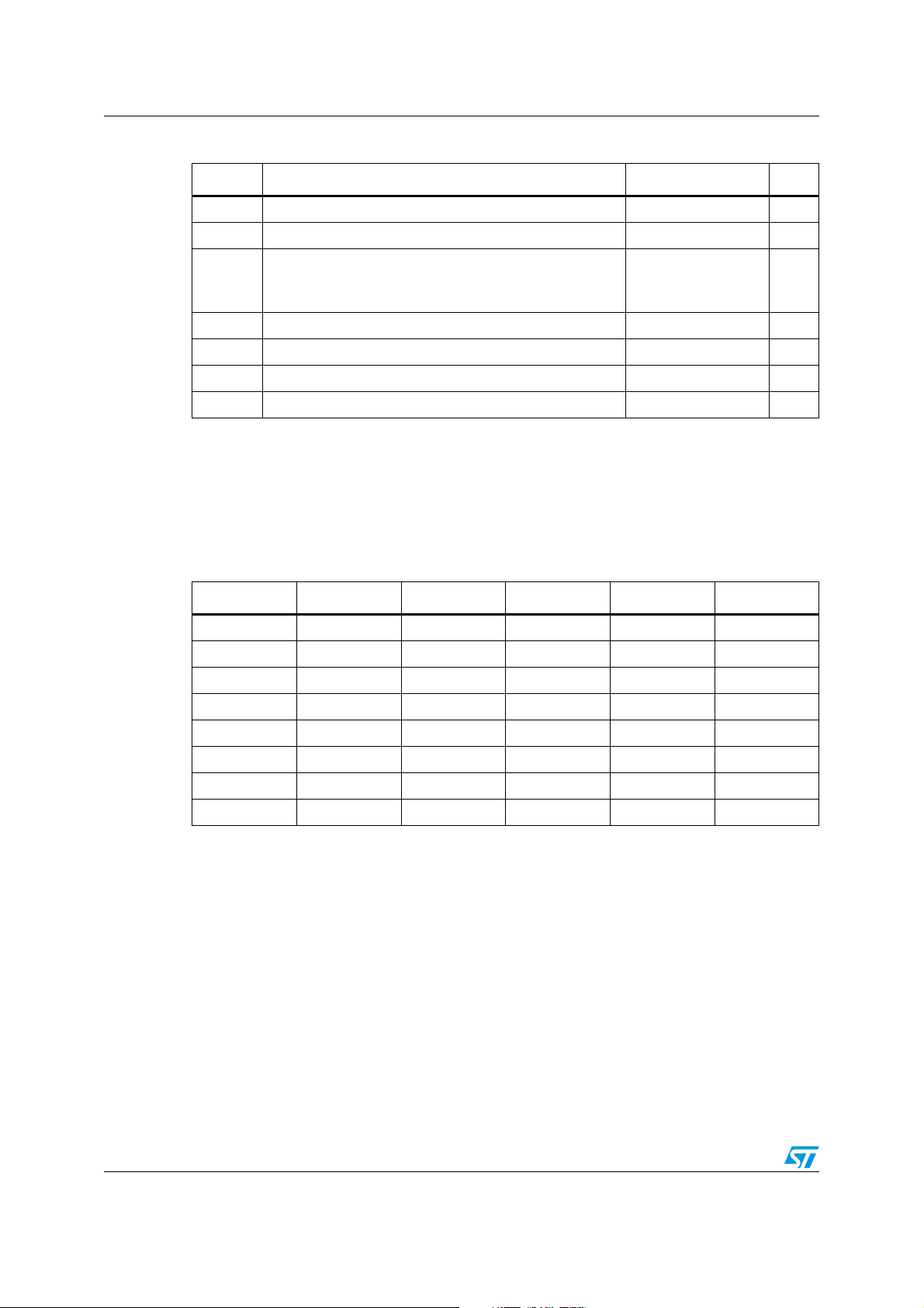
Table 2. Operating conditions
Symbol Parameter Value Unit
V
V
Supply voltage
CC
Input voltage range GND to V
in
Standby voltage input
VSTBY
Device ON
Device OFF
RL Load resistor
VIH G0, G1, 3D, High Level Input Voltage
VIL G0, G1, 3D, Low Level Input Voltage GND
R
1. For VCC from 2.4 to 2.5 V, the operating temperature range is reduced to 0° C ≤ T
2. Without any signal on V
3. Minimum current consumption is obtained when V
4. Between G0, G1, 3D pins and GND, there is an internal 300 kΩ (+/-20 %) pull-down resistor. When pins
are floating, the gain is 3.5 dB and 3D effect is off. In full standby (left and right channels OFF), these
resistors are disconnected (HiZ input).
5. With a 4-layer PCB.
Table 3. 3D effect pin and STANDBY pins setting truth table
Thermal Resistance Junction to Ambient
thja
(1)
(2)
(4)
(5)
, the device will be in standby (internal 300 kΩ (+/-20 %) pull down resistor)
STBY
= GND
STBY
2.4 to 5.5 V
1.4 ≤ V
GND ≤ V
≤ VCC
STBY
≤ 0.4
STBY
≥4 Ω
1.4 ≤ VIH ≤ VCC V
≤ VIL ≤ 0.4 V
90 °C/W
≤70° C
amb
CC
V
(3)
3D STBYL STBYR 3D Effect Left channel Right channel
0 0 0 X STDBY STDBY
001OFFSTDBYON
010OFFONSTDBY
011OFFONON
1 0 0 X STDBY STDBY
1 0 1 N/A N/A N/A
1 1 0 N/A N/A N/A
1 1 1 ON ON ON
Note: When the 3D effect is switched on, both channels must be in operation or in shutdown mode
at the same time.
4/36
Page 5
TS4999 Application information
2 Application information
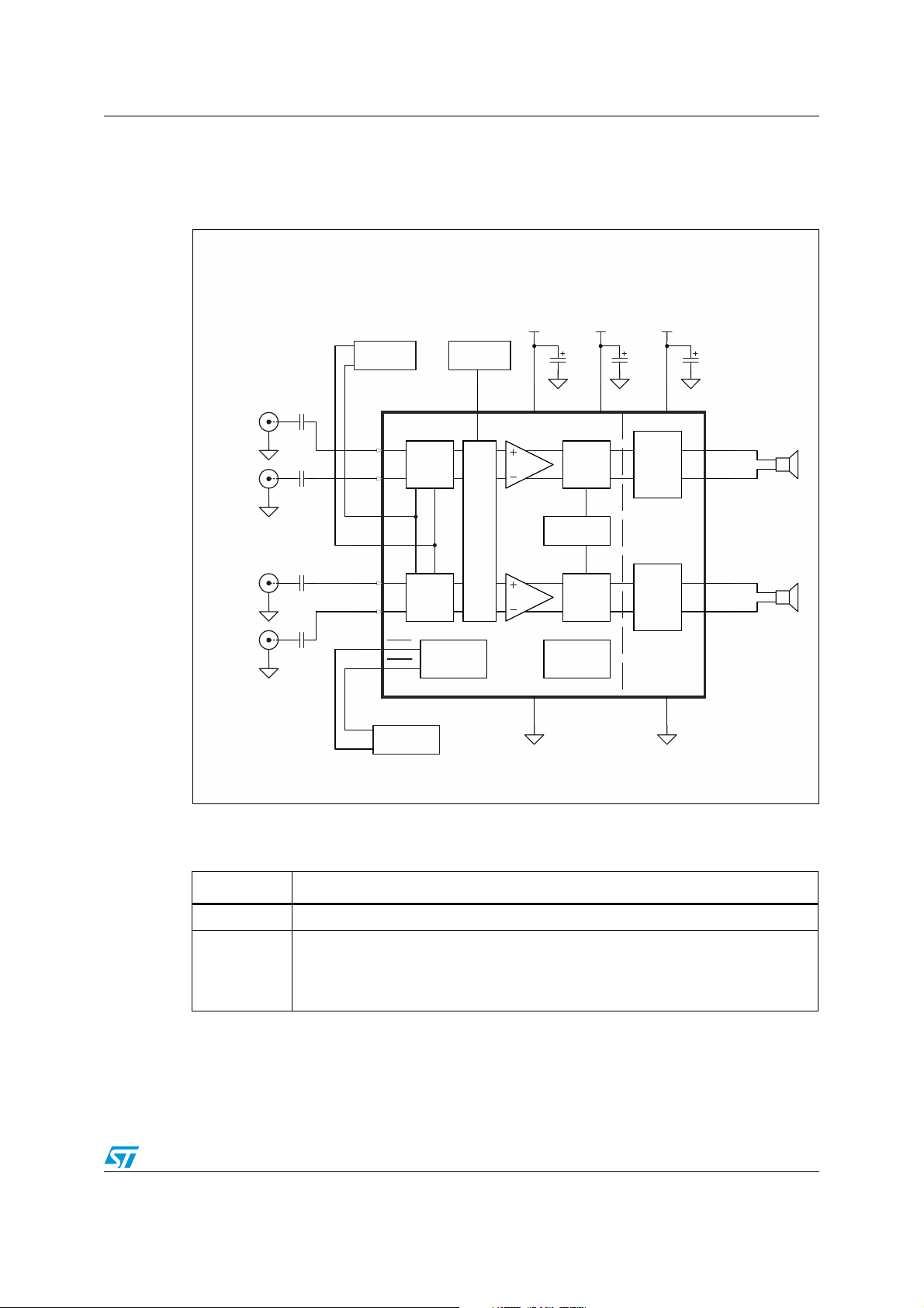
Figure 1. Typical application schematic
Differential
Left Input
Left IN+
Left IN-
Differential
Right Input
Right IN+
Right IN-
Cs
VCC VCC
0.1uF
Gain
3D Effect
Control
C13D
D4
AVCC
Oscillator
Gain Select
Control
TS49 99
Cin
Cin
Lin+
A1
Select
Lin-
B2
G0
C3
C5
G1
RPVCC
PWM
CsR
1uF
D6
VCC
LPVCC
H
Bridge
CsL
1uF
B6
Lout+
A5
A7
Lout-
Left speaker
3D EFFECT
E1
Rin+
Cin
Cin
D2
A3
E3
Gain
Select
Rin-
STBYL
STBYR
Standby Control
Standby
Control
PWM
Protection
Circuit
B4
H
Bridge
PGNDAGND
C7
Rout+
Rout-
E5
E7
Right speaker
Note: See Section 4.9: Output filter considerations on page 29.
Table 4. External component description
Components Functional description
, CSL, C
C
S
C
in
Supply capacitor that provides power supply filtering.
SR
Input coupling capacitors that block the DC voltage at the amplifier input terminal.
The capacitors also form a high pass filter with Z
(Fcl = 1 / (2 x π x Zin x Cin)). Note that the value of Z
These coupling capacitors are mandatory.
5/36
in
changes with each gain setting.
in
Page 6
Application information TS4999
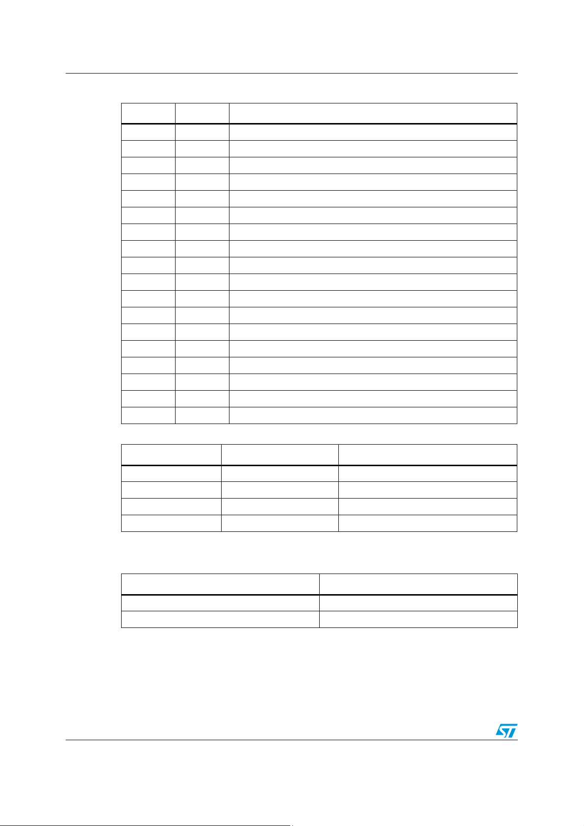
Table 5. Pin description
Bump Name Function
A1 LIN+ Left channel positive differential input
B2 LIN- Left channel negative differential input
C1 3D 3D effect digital input pin
E1 RIN+ Right channel positive differential input
D2 RIN- Right channel negative differential input
A3 STBYL Standby input pin (active low) for left channel output
C3 G0 Gain select input pin (LSB)
E3 STBYR Standby input pin (active low) for right channel output
B4 AGND Analog ground
D4 AVCC Analog supply voltage
A5 LOUT+ Left channel negative output
C5 G1 Gain select input pin (MSB)
E5 ROUT+ Right channel positive output
B6 LPVCC Left channel power supply voltage
D6 RPVCC Right channel power supply voltage
A7 LOUT- Left channel negative output
C7 PGND Power ground
E7 ROUT- Right channel negative output
Table 6. Truth table for output gain settings
G1 G0 Gain value (dB)
0 0 3.5
01 6
10 9.5
11 12
Note: See Table 3 on page 4.
Table 7. Truth table for 3D effects pin settings
3D 3D effect
0OFF
1ON
6/36
Page 7

TS4999 Electrical characteristics
3 Electrical characteristics
Table 8. VCC = +5 V, GND = 0 V, T
.
= 25° C (unless otherwise specified)
amb
Symbol Parameter Conditions Min. Typ. Max. Unit
I
I
STANDBY
Voo Output offset voltage
Supply current No input signal, no load, both channels 5 7 mA
CC
Standby current No input signal, Vstdby = GND 1 2 μA
Floating inputs, RL = 8Ω, G = 3.5dB,
3D effect off
20 mV
THD = 1% max, F = 1kHz, RL = 4Ω 2.25
Po Output power
THD+N
Total harmonic distortion +
noise
Efficiency Efficiency per channel
PSRR
Power supply rejection ratio
with inputs grounded
Crosstalk Channel separation
THD = 1% max, F = 1kHz, R
THD = 10% max, F = 1kHz, R
THD = 10% max, F = 1kHz, R
Po = 0.9W/Ch, G = 6dB, F=1kHz,
= 8Ω
R
L
Po = 2.3 W
Po = 1.4 W
= 1µF
C
in
, RL = 4Ω +15µH 82
RMS
, RL = 8Ω + 15µH 89
RMS
(1)
,3D effects off
F = 217Hz, RL = 8Ω, gain = 6dB,
Vripple = 200mVpp, Inputs grounded
F = 1kHz, R
= 8Ω,
L
3D effects off
= 8Ω 1.35
L
= 4Ω 2.8 W
L
= 8Ω 1.7 W
L
0.2 %
65 dB
100 dB
W
%
CMRR
Common mode rejection
ratio
Gain Gain value with no load
Single-ended input
IN
impedance referred to GND
Pulse width modulator
base frequency
F
Z
PWM
SNR Signal to noise ratio
t
WU
Wake-up time Total wake-up time
C
=1µF, F = 217Hz, RL = 8Ω, gain = 6dB,
in
ΔVIC = 200mVpp, 3D effects OFF
57 dB
G1 = G0 = "0" 3 3.5 4
G1 = "0" & G0 = "1" 5.5 6 6.5
dB
G1 = "1" & G0 = "0" 9 9.5 10
G1 = G0 = "1" 11.5 12 12.5
G1 = G0 = 3D = "0" or
G1 = "0" & G0 = "1" & 3D = "0" or
24 30 36 kΩ
G1 = "1" & G0 = "0" & 3D = "0"
G1 = "1" & G0 = "1" & 3D = "0" 12 15 18 kΩ
G1 = G0 = "0" & 3D = "1" or
G1 = "0" & G0 = "1" & 3D = "1" or
13.5 17.1 20.5 kΩ
G1 = "1" & G0 = "0" & 3D = "1"
G1 = "1" & G0 = "1" & G3D = "1" 6.5 8.6 10.5
190 280 370 kHz
= 1.3W, A-weighting, RL = 8Ω,
P
o
Gain = 6dB, 3D effects OFF
(2)
99 dB
9 13 16.5 ms
7/36
Page 8

Electrical characteristics TS4999
Table 8. VCC = +5 V, GND = 0 V, T
= 25° C (unless otherwise specified) (continued)
amb
Symbol Parameter Conditions Min. Typ. Max. Unit
t
STBY
Standby time Standby time
(2)
11 15.8 20 ms
F = 20Hz to 20kHz, A-weighted,
Gain = 3.5dB
Filterless, 3D effect off, R
Filterless, 3D effect on, RL = 4Ω
V
Output voltage noise
N
With LC output filter, 3D effect off, R
With LC output filter, 3D effect on, RL = 4Ω
Filterless, 3D effect off, RL = 8Ω
Filterless, 3D effect on, R
With LC output filter, 3D effect off, RL = 8Ω
With LC output filter, 3D effect on, RL = 8Ω
1. Dynamic measurements - 20*log(rms(Vout)/rms(Vripple)). Vripple is the super-imposed sinus signal to VCC at f = 217 Hz
with fixed Cin cap (input decoupling capacitor).
2. See Section 4.6: Wakeup (t
) and shutdown (t
WU
) times on page 26.
STBY
= 4Ω
L
= 8Ω
L
= 4Ω
L
31
50
30
48
32
51
31
50
μV
RMS
8/36
Page 9

TS4999 Electrical characteristics
Table 9. VCC = +3.6V, GND = 0V, T
.
= 25°C (unless otherwise specified)
amb
Symbol Parameter Conditions Min. Typ. Max. Unit
I
I
STANDBY
Voo Output offset voltage
Po Output power
THD+N
Efficiency Efficiency per channel
PSRR
Crosstalk Channel separation
CMRR
Supply current No input signal, no load, both channels 3.5 5.5 mA
CC
Standby current No input signal, Vstdby = GND 1 2 μA
Floating inputs, RL = 8Ω, G = 3.5dB,
3D effect off
= 4Ω 1.15
L
= 8Ω 0.7
L
= 4Ω 1.45 W
L
= 8Ω 0.86 W
L
0.15 %
64 dB
102 dB
55 dB
Total harmonic distortion +
noise
Power supply rejection ratio
with inputs grounded
Common mode rejection
ratio
THD = 1% max, F = 1kHz, R
THD = 1% max, F = 1kHz, R
THD = 10% max, F = 1kHz, R
THD = 10% max, F = 1kHz, R
Po = 0.45W/Ch, G = 6dB, F=1kHz,
= 8Ω
R
L
Po = 1.15 W
Po = 0.7 W
= 1µF
C
in
F = 217Hz, R
, RL = 4Ω +15µH 82
RMS
, RL = 8Ω + 15µH 89
RMS
(1)
,3D effects off
= 8Ω, gain = 6dB,
L
Vripple = 200mVpp, inputs grounded
F = 1kHz, R
= 8Ω,
L
3D effects off
=1µF, F = 217Hz, RL = 8Ω, gain = 6dB,
C
in
ΔVIC = 200mVpp, 3D effects off
20 mV
W
%
Gain Gain value with no load
Single-ended input
IN
impedance referred to GND
Pulse width modulator
base frequency
F
Z
PWM
SNR Signal to noise ratio
t
WU
Wake-up time Total wake-up time
G1 = G0 = "0" 3 3.5 4
G1 = "0" & G0 = "1" 5.5 6 6.5
dB
G1 = "1" & G0 = "0" 9 9.5 10
G1 = G0 = "1" 11.5 12 12.5
G1 = G0 = 3D = "0" or
G1 = "0" & G0 = "1" & 3D = "0" or
24 30 36 kΩ
G1 = "1" & G0 = "0" & 3D = "0"
G1 = "1" & G0 = "1" & 3D = "0" 12 15 18 kΩ
G1 = G0 = "0" & 3D = "1" or
G1 = "0" & G0 = "1" & 3D = "1" or
13.5 17.1 20.5 kΩ
G1 = "1" & G0 = "0" & 3D = "1"
G1 = "1" & G0 = "1" & G3D = "1" 6.5 8.6 10.5 kΩ
190 280 370 kHz
P
= 0.67W, A-weighting, RL = 8Ω,
o
Gain = 6dB, 3D effects OFF
(2)
97 dB
7.5 11.3 15 ms
9/36
Page 10

Electrical characteristics TS4999
Table 9. VCC = +3.6V, GND = 0V, T
= 25°C (unless otherwise specified) (continued)
amb
Symbol Parameter Conditions Min. Typ. Max. Unit
t
STBY
Standby time Standby time
(2)
10 13.8 18 ms
F = 20Hz to 20kHz, A-Weighted,
Gain = 3.5dB
Filterless, 3D effect off, R
Filterless, 3D effect on, RL = 4Ω
V
Output voltage noise
N
With LC output filter, 3D effect off, R
With LC output filter, 3D effect on, RL = 4Ω
Filterless, 3D effect off, RL = 8Ω
Filterless, 3D effect on, R
With LC output filter, 3D effect off, RL = 8Ω
With LC output filter, 3D effect on, RL = 8Ω
1. Dynamic measurements - 20*log(rms(Vout)/rms(Vripple)). Vripple is the super-imposed sinus signal to VCC at f = 217 Hz
with fixed Cin cap (input decoupling capacitor).
2. See Section 4.6: Wakeup (t
) and shutdown (t
WU
) times on page 26.
STBY
= 4Ω
L
= 8Ω
L
= 4Ω
L
29
49
28
48
29
50
29
50
μV
RMS
10/36
Page 11
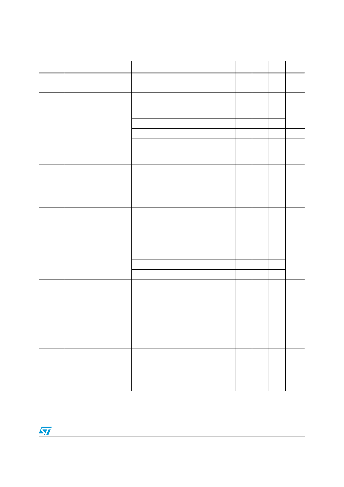
TS4999 Electrical characteristics
Table 10. VCC = +2.5 V, GND = 0V, T
= 25° C (unless otherwise specified)
amb
Symbol Parameter Conditions Min. Typ. Max. Unit
I
I
STANDBY
Voo Output offset voltage
Po Output power
THD+N
Efficiency Efficiency per channel
PSRR
Crosstalk Channel separation
CMRR
Supply current No input signal, no load, both channels 2.8 4 mA
CC
Standby current No input signal, Vstdby = GND 1 2 μA
Floating inputs, RL = 8Ω, G = 3.5dB,
3D effect off
= 4Ω 0.53
L
= 8Ω 0.33
L
= 4Ω 0.67 W
L
= 8Ω 0.4 W
L
0.07 %
63 dB
104 dB
55 dB
Total harmonic distortion +
noise
Power supply rejection ratio
with inputs grounded
Common mode rejection
ratio
THD = 1% max, F = 1kHz, R
THD = 1% max, F = 1kHz, R
THD = 10% max, F = 1kHz, R
THD = 10% max, F = 1kHz, R
Po = 0.2W/Ch, G = 6dB, F=1kHz,
= 8Ω
R
L
Po = 0.52 W
Po = 0.33 W
= 1µF
C
in
F = 217Hz, R
, RL = 4Ω +15µH 81
RMS
, RL = 8Ω + 15µH 88
RMS
(1)
,3D effects off
= 8Ω, gain = 6dB,
L
Vripple = 200mVpp, Inputs grounded
F = 1kHz, R
= 8Ω,
L
3D effects off
=1µF, F = 217Hz, RL = 8Ω, gain = 6dB,
C
in
ΔVIC = 200mVpp, 3D effects off
20 mV
W
%
Gain Gain value with no load
Single-ended input
IN
impedance referred to GND
Pulse width modulator
base frequency
F
Z
PWM
SNR Signal to noise ratio
t
WU
Wake-up time Total wake-up time
G1 = G0 = "0" 3 3.5 4
G1 = "0" & G0 = "1" 5.5 6 6.5
dB
G1 = "1" & G0 = "0" 9 9.5 10
G1 = G0 = "1" 11.5 12 12.5
G1 = G0 = 3D = "0" or
G1 = "0" & G0 = "1" & 3D = "0" or
24 30 36 kΩ
G1 = "1" & G0 = "0" & 3D = "0"
G1 = "1" & G0 = "1" & 3D = "0" 12 15 18 kΩ
G1 = G0 = "0" & 3D = "1" or
G1 = "0" & G0 = "1" & 3D = "1" or
13.5 17.1 20.5 kΩ
G1 = "1" & G0 = "0" & 3D = "1"
G1 = "1" & G0 = "1" & G3D = "1" 6.5 8.6 10.5 kΩ
190 280 370 kHz
P
= 0.3W, A-weighting, RL = 8Ω,
o
Gain = 6dB, 3D effects OFF
(2)
94 dB
37.812ms
11/36
Page 12
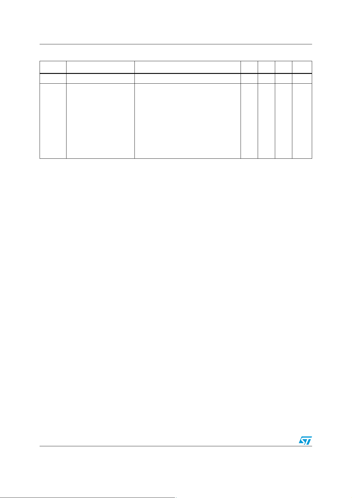
Electrical characteristics TS4999
Table 10. VCC = +2.5 V, GND = 0V, T
= 25° C (unless otherwise specified) (continued)
amb
Symbol Parameter Conditions Min. Typ. Max. Unit
t
STBY
Standby time Standby time
(2)
81216ms
F = 20Hz to 20kHz, A-Weighted,
Gain = 3.5dB
Filterless, 3D effect off, R
Filterless, 3D effect on, RL = 4Ω
V
Output voltage noise
N
With LC output filter, 3D effect off, R
With LC output filter, 3D effect on, RL = 4Ω
Filterless, 3D effect off, RL = 8Ω
Filterless, 3D effect on, R
With LC output filter, 3D effect off, RL = 8Ω
With LC output filter, 3D effect on, RL = 8Ω
1. Dynamic measurements - 20*log(rms(Vout)/rms(Vripple)). Vripple is the super-imposed sinus signal to VCC at f = 217 Hz
with fixed Cin cap (input decoupling capacitor).
2. See Section 4.6: Wakeup (t
) and shutdown (t
WU
) times on page 26.
STBY
= 4Ω
L
= 8Ω
L
= 4Ω
L
28
47
27
45
28
48
28
47
μV
RMS
12/36
Page 13
TS4999 Electrical characteristics
3.1 Electrical characteristic curves
The graphs shown in this section use the following abbreviations.
● R
● Filter = LC output filter (1 µF+ 30 µH for 4 Ω and 0.5 µF+15 µH for 8 Ω).
+ 15 µH or 30 µH = pure resistor + very low series resistance inductor.
L
All measurements are done with C
for the PSRR where C
SL
, C
SR
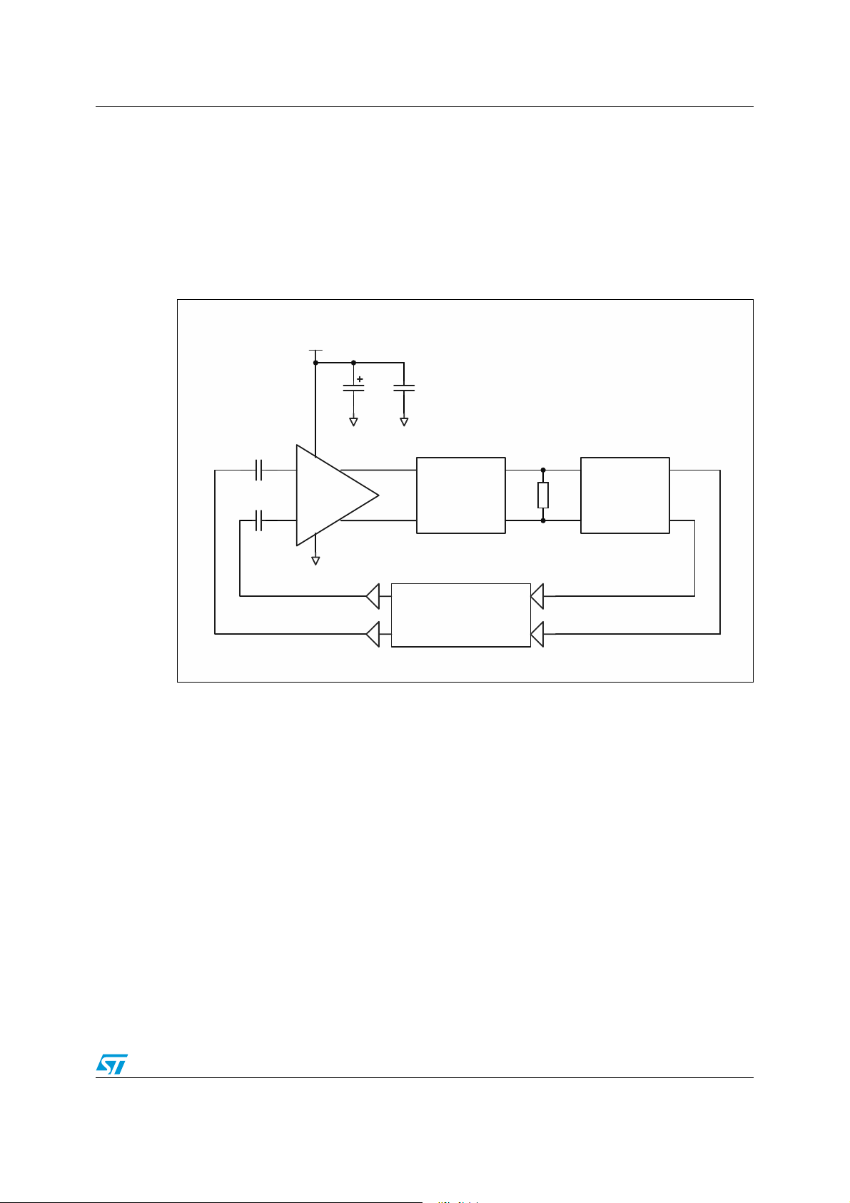
= CSR=1 µF and CS = 100 nF (see Figure 2), except
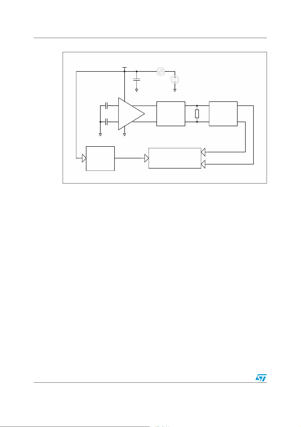
SL
is removed (see Figure 3).
Figure 2. Measurement test diagram
Cin
Cin
CsL
(CsR)
VCC
In+
1/2 TS4999
In-
GN D
1 F
GN D GN D
Out+
Out-
μ
Cs
100nF
15 H or 30 H
Audio Measurement
Bandwith < 30kHz
μμ
or
LC Filter
RL
4 or 8
Ω
5th order
50kHz
low-pass filter
13/36
Page 14
Electrical characteristics TS4999
Figure 3. PSRR measurement test diagram
Cs
VCC
100nF
20Hz to 20kHz
μ
1 F
Cin
Cin
μ
1 F
GN D
5th order
50kHz
low-pass filter
GN D
Out+
In+
1/2 TS4999
In-
Out-
GN D
reference
Vripple
Vcc
GN D
4 or 8
μμ
15 H or 30 H
or
LC Filter
RM S Sel e cti v e Meas u re me n t
Band wit h = 1% of Fm ea s
RL
Ω
5th order
50kHz
low-pass filter
14/36
Page 15
TS4999 Electrical characteristics
Effi
i
(
)
Dissipated Power (W)
Efficiency
(%)
Dissipated Power (W)
Efficiency
(%)
Dissipated Power (W)
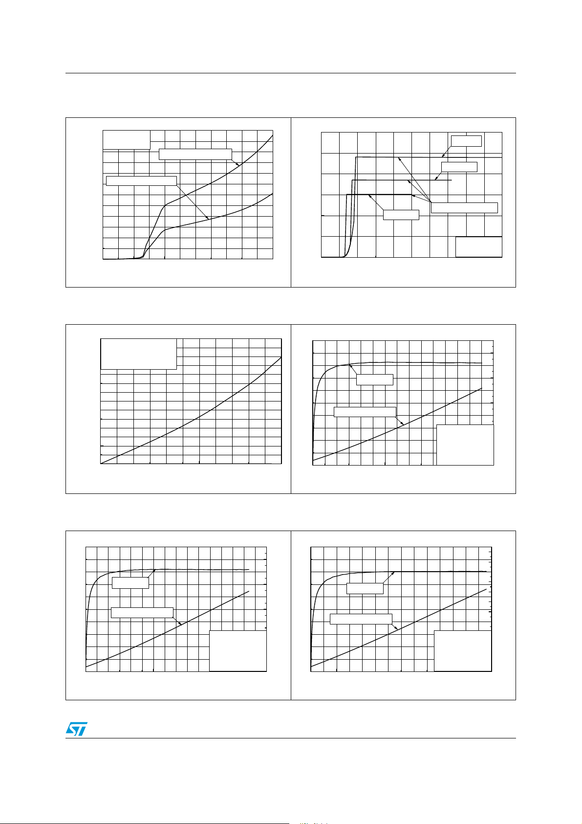
Figure 4. Current consumption vs. power
supply voltage
6
No load
Tamb = 25°C
5
4
One channel active
3
2
1
Current Consumption (mA)
0
012345
Both channels active
Power Supply Voltage (V)
Figure 6. Standby current consumption vs.
power supply voltage
1.4
No load
V
= V
STBYL
1.2
Tamb = 25°C
1.0
A)
μ
0.8
0.6
0.4
Standby Current (
0.2
0.0
012345
= GND
STBYR
Power Supply Voltage (V)
Figure 5. Current consumption vs. standby
voltage (one channel)
3
2
1
Current Consumption (mA)
0
012345
Vcc=2.5V
Standby Voltage (V)
Vcc=5V
Vcc=3.6V
One channel active
No load
Tamb = 25°C
Figure 7. Efficiency vs. output power
(one channel)
100
80
%
60
ency
c
40
20
0
0.0 0.4 0.8 1.2 1.6 2.0 2.4 2.8
Efficiency
Power dissipation
Vcc = 5V
RL = 4Ω + 15μH
F = 1kHz
THD+N ≤ 10%
Output Power (W)
1.0
0.9
0.8
0.7
0.6
0.5
0.4
0.3
0.2
0.1
0.0
Figure 8. Efficiency vs. output power
(one channel)
100
80
Efficiency
60
40
20
0
0.0 0.2 0.4 0.6 0.8 1.0 1.2 1.4 1.6
Power dissipation
Output Power (W)
Vcc = 3.6V
RL = 4Ω + 15μH
F = 1kHz
THD+N ≤ 10%
Figure 9. Efficiency vs. output power
(one channel)
100
0.50
0.45
0.40
0.35
0.30
0.25
0.20
0.15
0.10
0.05
0.00
80
60
40
20
0
0.0 0.1 0.2 0.3 0.4 0.5 0.6 0.7
Efficiency
Power dissipation
Vcc = 2.5V
RL = 4Ω + 15μH
F = 1kHz
THD+N ≤ 10%
Output Power (W)
15/36
0.24
0.22
0.20
0.18
0.16
0.14
0.12
0.10
0.08
0.06
0.04
0.02
0.00
Page 16
Electrical characteristics TS4999
Efficiency
(%)
Dissipated Power (W)
Efficiency
(%)
Dissipated Power (W)
Efficiency
(%)
Dissipated Power (W)
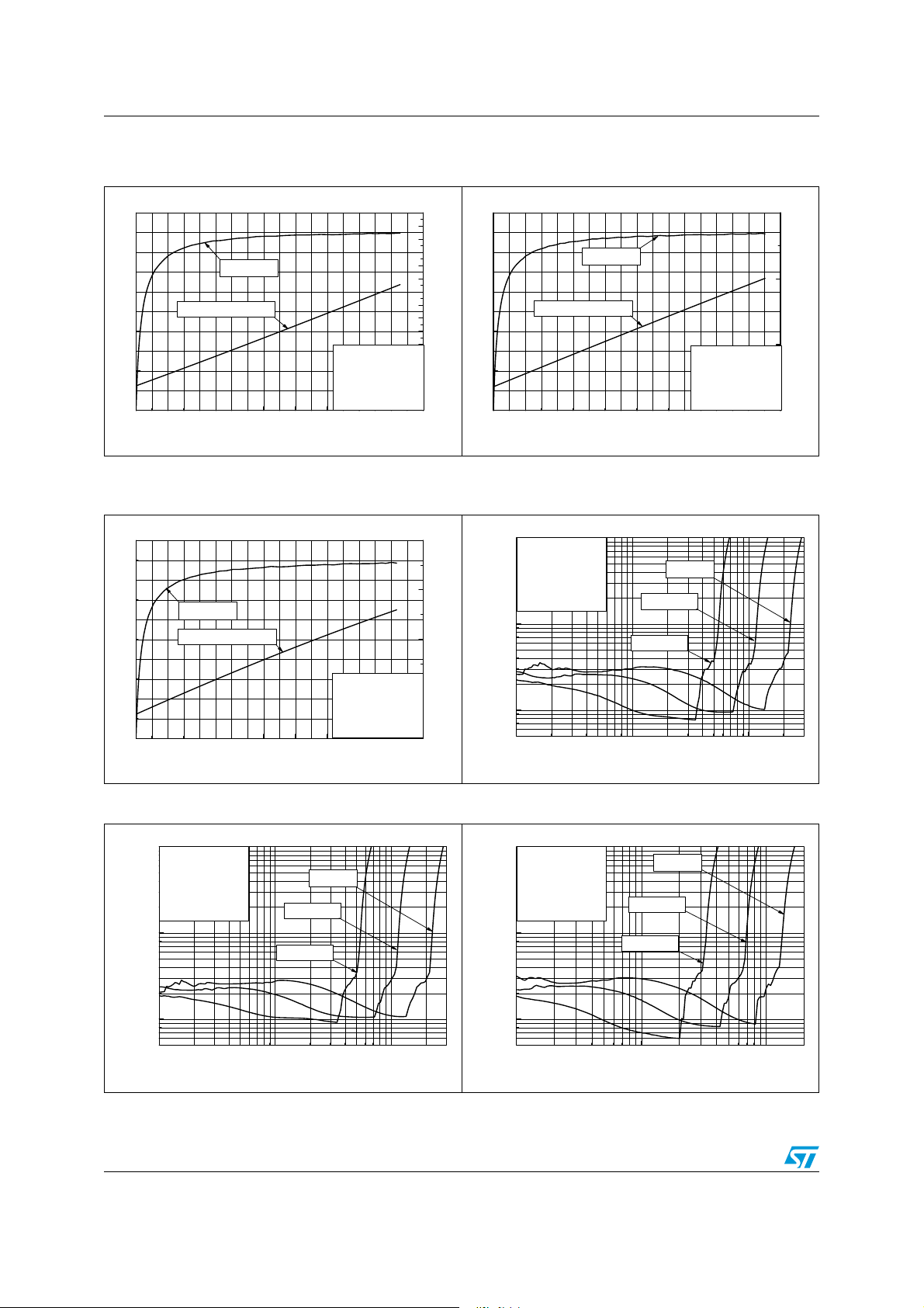
Figure 10. Efficiency vs. output power
(one channel)
100
80
Efficiency
60
40
20
0
0.0 0.2 0.4 0.6 0.8 1.0 1.2 1.4 1.6 1.8
Power dissipation
Vcc = 5V
RL = 8Ω + 15μH
F = 1kHz
THD+N ≤ 10%
Output Power (W)
Figure 12. Efficiency vs. output power
(one channel)
100
80
60
40
20
0
0.00 0.05 0.10 0.15 0.20 0.25 0.30 0.35 0.40 0.45
Efficiency
Power dissipation
Vcc = 2.5V
RL = 8Ω + 15μH
F = 1kHz
THD+N ≤ 10%
Output Power (W)
Figure 11. Efficiency vs. output power
(one channel)
0.30
100
0.28
0.26
0.24
0.22
0.20
0.18
0.16
0.14
0.12
0.10
0.08
0.06
0.04
0.02
0.00
80
60
40
20
0
0.00.10.20.30.40.50.60.70.80.9
Power dissipation
Efficiency
Output Power (W)
Figure 13. THD+N vs. output power
0.08
0.06
0.04
0.02
0.00
10
F = 1kHz
RL = 4Ω + 15μH
G = +6dB
BW < 30kHz
Tamb = 25°C
1
THD + N (%)
0.1
0.01 0.1 1
Vcc=3.6V
Vcc=2.5V
Output power (W)
Vcc = 3.6V
RL = 8Ω + 15μH
F = 1kHz
THD+N ≤ 10%
Vcc=5V
0.15
0.10
0.05
0.00
Figure 14. THD+N vs. output power Figure 15. THD+N vs. output power
10
F = 1kHz
RL = 4Ω + 30μH
G = +6dB
BW < 30kHz
Tamb = 25°C
1
THD + N (%)
0.1
0.01 0.1 1
Output power (W)
Vcc=5V
Vcc=3.6V
Vcc=2.5V
16/36
10
F = 1kHz
RL = 8Ω + 15μH
G = +6dB
BW < 30kHz
Tamb = 25°C
1
THD + N (%)
0.1
0.01 0.1 1
Vcc=5V
Vcc=3.6V
Vcc=2.5V
Output power (W)
Page 17
TS4999 Electrical characteristics
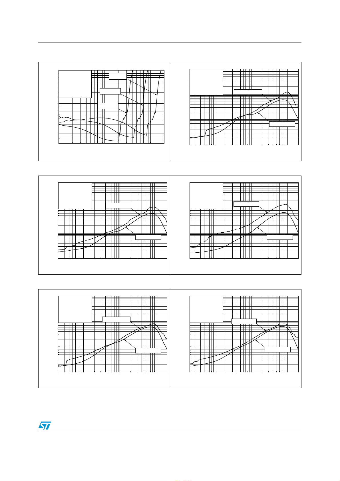
Figure 16. THD+N vs. output power Figure 17. THD+N vs. frequency
THD + N (%)
10
1
0.1
0.01
Vcc = 5V
RL = 4Ω + 15μH
G = +6dB
BW < 30kHz
Tamb = 25°C
20
Po=1500mW
100 1000 10000
Frequency (Hz)
10
F = 1kHz
RL = 8Ω + 30μH
G = +6dB
BW < 30kHz
Tamb = 25°C
1
THD + N (%)
0.1
0.01 0.1 1
Vcc=5V
Vcc=3.6V
Vcc=2.5V
Output power (W)
Figure 18. THD+N vs. frequency Figure 19. THD+N vs. frequency
THD + N (%)
10
0.1
Vcc = 3.6V
RL = 4Ω + 15μH
G = +6dB
BW < 30kHz
Tamb = 25°C
1
Po=800mW
Po=400mW
THD + N (%)
10
1
0.1
Vcc = 2.5V
RL = 4Ω + 15μH
G = +6dB
BW < 30kHz
Tamb = 25°C
Po=400mW
Po=750mW
Po=200mW
0.01
20 100 1000 10000
100 1000 10000
Frequency (Hz)
v
0.01
20
Frequency (Hz)
Figure 20. THD+N vs. frequency Figure 21. THD+N vs. frequency
THD + N (%)
10
1
0.1
0.01
Vcc = 5V
RL = 4Ω + 30μH
G = +6dB
BW < 30kHz
Tamb = 25°C
20
Po=1500mW
Po=750mW
100 1000 10000
Frequency (Hz)
THD + N (%)
10
1
0.1
0.01
Vcc = 3.6V
RL = 4Ω + 30μH
G = +6dB
BW < 30kHz
Tamb = 25°C
20
Po=800mW
100 1000 10000
Frequency (Hz)
Po=400mW
17/36
Page 18
Electrical characteristics TS4999
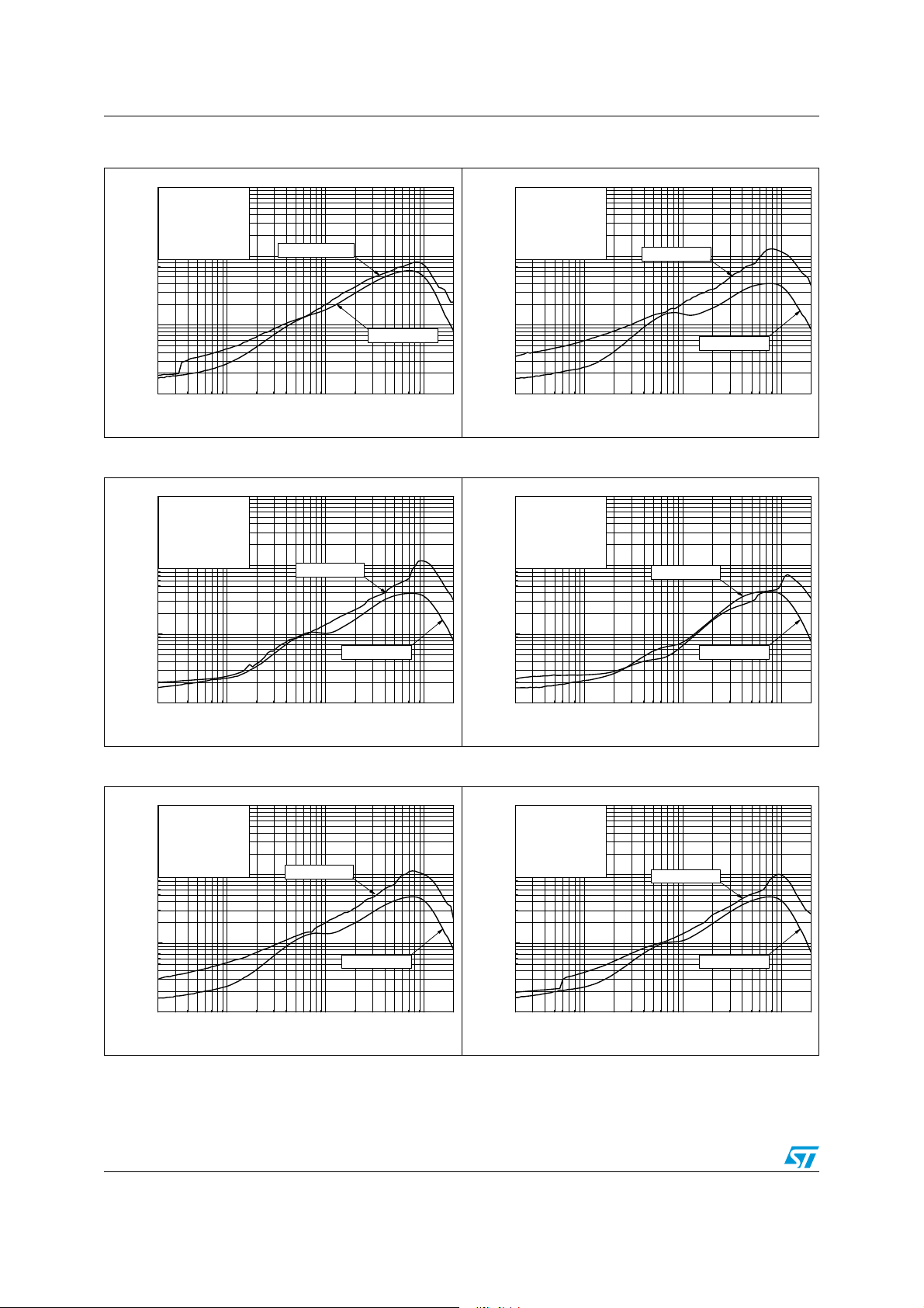
Figure 22. THD+N vs. frequency Figure 23. THD+N vs. frequency
THD + N (%)
10
0.1
0.01
Vcc = 5V
RL = 4Ω + 30μH
G = +6dB
BW < 30kHz
Tamb = 25°C
1
20
Po=1500mW
Po=750mW
100 1000 10000
Frequency (Hz)
THD + N (%)
10
1
0.1
0.01
Vcc = 5V
RL = 8Ω + 15μH
G = +6dB
BW < 30kHz
Tamb = 25°C
20
Po=900mW
100 1000 10000
Frequency (Hz)
Figure 24. THD+N vs. frequency Figure 25. THD+N vs. frequency
THD + N (%)
10
0.1
Vcc = 3.6V
RL = 8Ω + 15μH
G = +6dB
BW < 30kHz
Tamb = 25°C
1
Po=450mW
Po=225mW
THD + N (%)
10
1
0.1
Vcc = 2.5V
RL = 8Ω + 15μH
G = +6dB
BW < 30kHz
Tamb = 25°C
Po=200mW
Po=450mW
Po=100mW
0.01
20
100 1000 10000
Frequency (Hz)
0.01
20
100 1000 10000
Frequency (Hz)
Figure 26. THD+N vs. frequency Figure 27. THD+N vs. frequency
THD + N (%)
10
1
0.1
0.01
Vcc = 5V
RL = 8Ω + 30μH
G = +6dB
BW < 30kHz
Tamb = 25°C
20
Po=900mW
Po=450mW
100 1000 10000
Frequency (Hz)
THD + N (%)
10
1
0.1
0.01
Vcc = 3.6V
RL = 8Ω + 30μH
G = +6dB
BW < 30kHz
Tamb = 25°C
20
Po=450mW
100 1000 10000
Frequency (Hz)
Po=225mW
18/36
Page 19
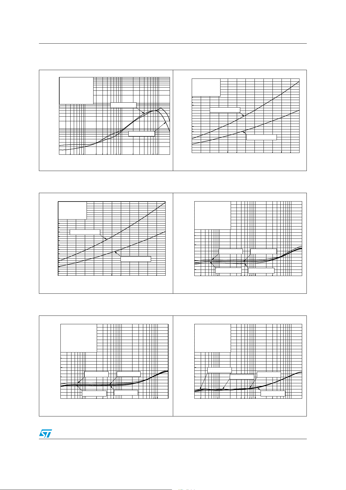
TS4999 Electrical characteristics
Figure 28. THD+N vs. frequency Figure 29. Output power vs. power supply
voltage
10
Vcc = 2.5V
RL = 8Ω + 30μH
G = +6dB
BW < 30kHz
Tamb = 25°C
THD + N (%)
0.1
0.01
1
20
100 1000 10000
Po=200mW
Po=100mW
Frequency (Hz)
Figure 30. Output power vs. power supply
voltage
3.4
F = 1kHz
3.2
3.0
BW < 30kHz
2.8
Tamb = 25°C
2.6
2.4
2.2
2.0
1.8
1.6
1.4
1.2
1.0
0.8
0.6
0.4
Output power at 10% THD + N (W)
0.2
0.0
RL=4Ω +≥15μH
RL=8Ω +≥15μH
2.5 3.0 3.5 4.0 4.5 5.0 5.5
Supply voltage (V)
2.8
F = 1kHz
2.6
BW < 30kHz
2.4
Tamb = 25°C
2.2
2.0
1.8
1.6
1.4
1.2
1.0
0.8
0.6
0.4
Output power at 1% THD + N (W)
0.2
0.0
2.5 3.0 3.5 4.0 4.5 5.0 5.5
RL=4Ω +≥15μH
RL=8Ω +≥15μH
Supply voltage (V)
Figure 31. Crosstalk vs. frequency
(3D effect off)
0
Vcc = 5V
-10
RL = 4Ω +≥15μH
-20
G = +6dB
-30
Cin = 1μF
Tamb = 25°C
-40
-50
-60
-70
Crosstalk Level (dB)
-80
-90
-100
-110
-120
20
Po=500mW
Po=1500mW
100 1000 10000
Frequency (Hz)
Po=1000mW
Po=1800mW
Figure 32. Crosstalk vs. frequency
(3D effect off)
0
Vcc = 3.6V
-10
RL = 4Ω +≥15μH
-20
G = +6dB
-30
Cin = 1μF
Tamb = 25°C
-40
-50
-60
-70
Crosstalk Level (dB)
-80
-90
-100
-110
-120
Po=250mW
Po=750mW
20
100 1000 10000
Frequency (Hz)
Po=500mW
Po=900mW
Figure 33. Crosstalk vs. frequency
(3D effect off)
0
Vcc = 2.5V
-10
RL = 4Ω +≥15μH
-20
G = +6dB
-30
Cin = 1μF
Tamb = 25°C
-40
-50
-60
-70
-80
Crosstalk Level (dB)
-90
-100
-110
-120
19/36
20
Po=125mW
Po=250mW
100 1000 10000
Frequency (Hz)
Po=325mW
Po=450mW
Page 20
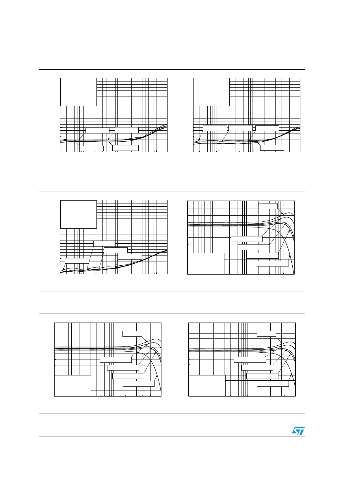
Electrical characteristics TS4999
Figure 34. Crosstalk vs. frequency
(3D effect off)
0
Vcc = 5V
-10
RL = 8Ω +≥15μH
-20
G = +6dB
-30
Cin = 1μF
Tamb = 25°C
-40
-50
-60
-70
Crosstalk Level (dB)
-80
-90
-100
-110
-120
Po=300mW
Po=900mW
20
100 1000 10000
Po=600mW
Po=1100mW
Frequency (Hz)
Figure 36. Crosstalk vs. frequency
(3D effect off)
0
Vcc = 2.5V
-10
RL = 8Ω +≥15μH
-20
G = +6dB
-30
Cin = 1μF
Tamb = 25°C
-40
-50
-60
Crosstalk Level (dB)
-70
-80
-90
-100
-110
-120
Po=150mW
20
Po=75mW
Po=225mW
Po=270mW
100 1000 10000
Frequency (Hz)
Figure 35. Crosstalk vs. frequency
(3D effect off)
0
Vcc = 3.6V
-10
RL = 8Ω +≥15μH
-20
G = +6dB
-30
Cin = 1μF
Tamb = 25°C
-40
-50
-60
-70
Crosstalk Level (dB)
-80
-90
-100
-110
-120
20
Po=160mW
Po=320mW
100 1000 10000
Frequency (Hz)
Po=500mW
Po=600mW
Figure 37. Gain vs. frequency
(3D effect off)
5
4
3
Gain (dB)
2
Gain = 3.5dB
1
Vin = 400mVrms
Cin = 10μF
Tamb = 25°C
0
20
RL=8Ω+15μH
RL=8Ω+30μH
100 1k 10k
Frequency (Hz)
no load
RL=4Ω+15μH
RL=4Ω+30μH
20k
Figure 38. Gain vs. frequency
(3D effect off)
8
7
6
5
Gain (dB)
4
Gain = 6dB
Vin = 300mVrms
3
Cin = 10μF
Tamb = 25°C
2
20
100 1k 10k
RL=8Ω+15μH
Frequency (Hz)
20/36
no load
RL=8Ω+30μH
RL=4Ω+15μH
RL=4Ω+30μH
20k
Figure 39. Gain vs. frequency
(3D effect off)
12
11
10
9
8
Gain (dB)
7
Gain = 9.5dB
Vin = 200mVrms
6
Cin = 10μF
Tamb = 25°C
5
20
100 1k 10k
RL=8Ω+15μH
RL=8Ω+30μH
RL=4Ω+15μH
Frequency (Hz)
no load
RL=4Ω+30μH
20k
Page 21
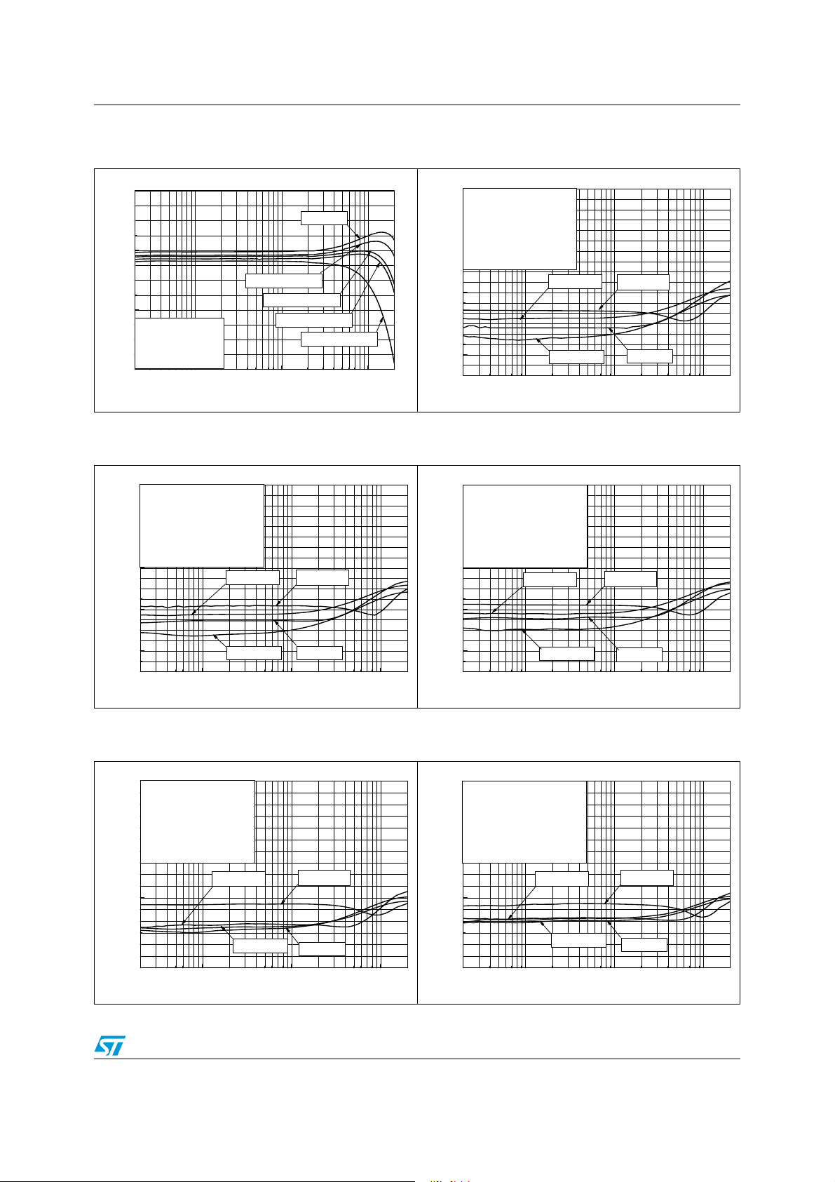
TS4999 Electrical characteristics
Figure 40. Gain vs. frequency
(3D effect off)
14
13
12
11
Gain (dB)
10
Gain = 12dB
Vin = 150mVrms
9
Cin = 10μF
Tamb = 25°C
8
20
100 1k 10k
RL=8Ω+15μH
RL=8Ω+30μH
RL=4Ω+15μH
Frequency (Hz)
Figure 42. PSRR vs. frequency
(3D effect off)
0
Inputs grounded
-10
Vcc = 3.6V, 3D effect off
Vripple = 200mVpp
-20
Cin = 10μF
RL = 8Ω +≥ 15μH
-30
Tamb = 25°C
-40
-50
PSRR (dB)
-60
-70
-80
-90
20
G=+9.5dB
G=+3.5dB
100 1000 10000
Frequency (Hz)
no load
RL=4Ω+30μH
G=+12dB
G=+6dB
Figure 41. PSRR vs. frequency
(3D effect off)
0
Inputs grounded
-10
Vcc = 5V, 3D effect off
Vripple = 200mVpp
-20
Cin = 10μF
RL = 8Ω +≥ 15μH
-30
Tamb = 25°C
20k
-40
-50
PSRR (dB)
-60
-70
-80
-90
20
G=+9.5dB
G=+3.5dB
100 1000 10000
Frequency (Hz)
Figure 43. PSRR vs. frequency
(3D effect off)
0
Inputs grounded
-10
Vcc = 2.5V, 3D effect off
Vripple = 200mVpp
-20
Cin = 10μF
RL = 8Ω +≥ 15μH
-30
Tamb = 25°C
-40
-50
PSRR (dB)
-60
-70
-80
-90
20
G=+9.5dB
G=+3.5dB
100 1000 10000
Frequency (Hz)
G=+12dB
G=+6dB
G=+12dB
G=+6dB
Figure 44. PSRR vs. frequency
(3D effect on)
0
Inputs grounded
-10
Vcc = 5V, 3D effect on
Vripple = 200mVpp
-20
Cin = 10μF
RL = 8Ω +≥15μH
-30
Tamb = 25°C
-40
-50
PSRR (dB)
-60
-70
-80
20
G=+9.5dB
G=+3.5dB
100 1000 10000
Frequency (Hz)
G=+12dB
G=+6dB
Figure 45. PSRR vs. frequency
(3D effect on)
0
Inputs grounded
-10
Vcc = 3.6V, 3D effect on
Vripple = 200mVpp
-20
Cin = 10μF
RL = 8Ω +≥ 15μH
-30
Tamb = 25°C
-40
-50
PSRR (dB)
-60
-70
-80
20
G=+9.5dB
G=+3.5dB
100 1000 10000
Frequency (Hz)
21/36
G=+12dB
G=+6dB
Page 22
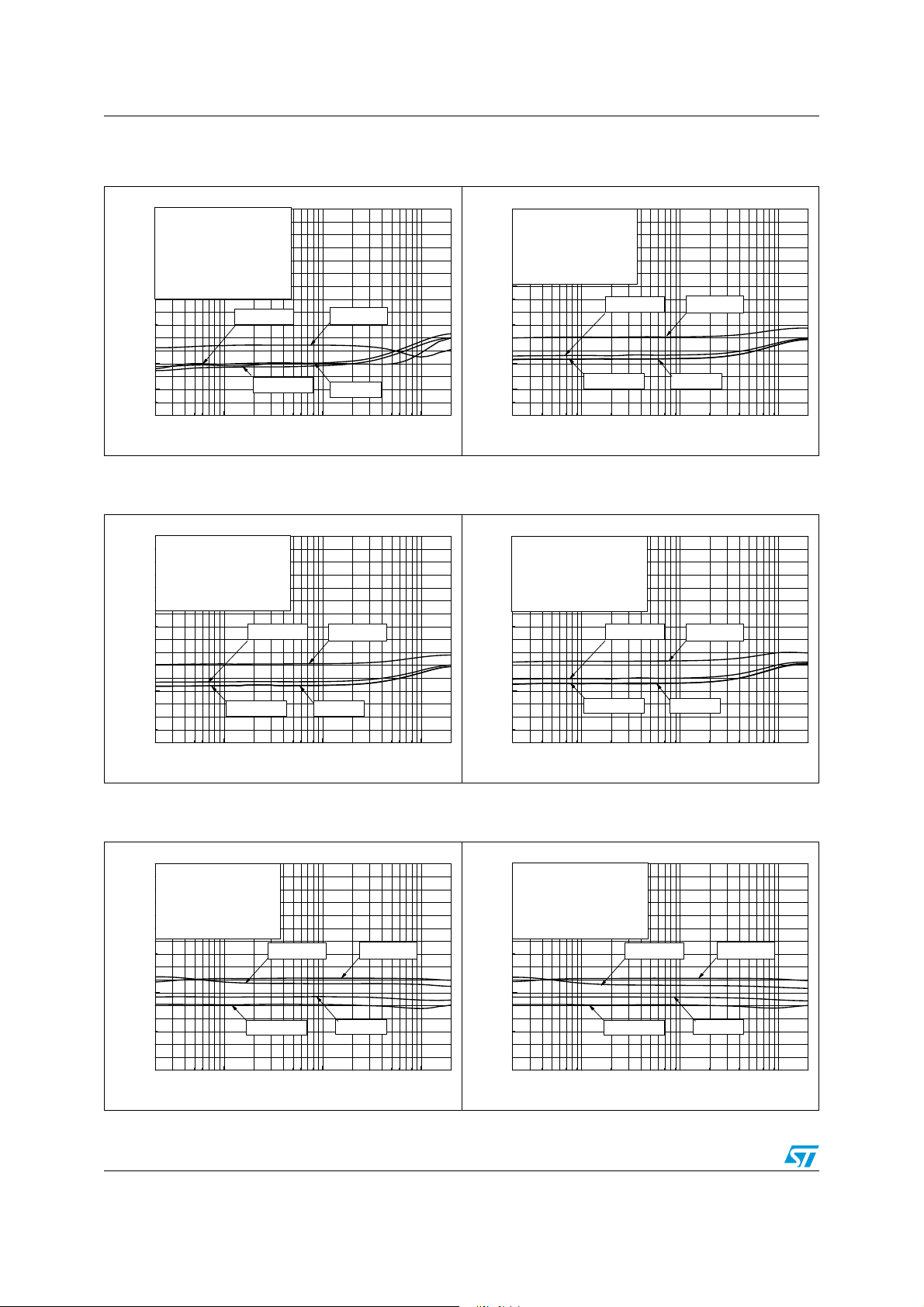
Electrical characteristics TS4999
Figure 46. PSRR vs. frequency
(3D effect on)
0
Inputs grounded
Vcc = 2.5V, 3D effect on
-10
Vripple = 200mVpp
-20
Cin = 10μF
RL = 8Ω +≥ 15μH
-30
Tamb = 25°C
-40
-50
PSRR (dB)
-60
-70
-80
20
G=+9.5dB
G=+3.5dB
100 1000 10000
Frequency (Hz)
Figure 48. CMRR vs. frequency
(3D effect off)
0
Vcc = 3.6V, 3D effect off
Δ
Vic = 200mVpp
-10
Cin = 10μF
RL = 8Ω +≥ 15μH
-20
Tamb = 25°C
-30
-40
-50
CMRR(dB)
-60
-70
-80
20
G=+9.5dB
G=+3.5dB
100 1000 10000
Frequency (Hz)
G=+6dB
G=+12dB
G=+6dB
G=+12dB
Figure 47. CMRR vs. frequency
(3D effect off)
0
Vcc = 5V, 3D effect off
ΔVic = 200mVpp
-10
Cin = 10μF
RL = 8Ω +≥ 15μH
-20
Tamb = 25°C
-30
-40
-50
CMRR(dB)
-60
-70
-80
20
G=+9.5dB
G=+3.5dB
100 1000 10000
Frequency (Hz)
G=+12dB
G=+6dB
Figure 49. CMRR vs. frequency
(3D effect off)
0
Vcc = 2.5V, 3D effect off
ΔVic = 200mVpp
-10
Cin = 10μF
RL = 8Ω +≥ 15μH
-20
Tamb = 25°C
-30
-40
-50
CMRR(dB)
-60
-70
-80
20
G=+9.5dB
G=+3.5dB
100 1000 10000
Frequency (Hz)
G=+12dB
G=+6dB
Figure 50. CMRR vs. frequency
(3D effect on)
0
Vcc = 5V, 3D effect on
Δ
Vic = 200mVpp
-10
Cin = 10μF
RL = 8Ω +≥ 15μH
-20
Tamb = 25°C
-30
-40
-50
CMRR(dB)
-60
-70
-80
20
100 1000 10000
G=+9.5dB
G=+3.5dB
Frequency (Hz)
22/36
G=+12dB
G=+6dB
Figure 51. CMRR vs. frequency
(3D effect on)
0
Vcc = 3.6V, 3D effect on
Δ
Vic = 200mVpp
-10
Cin = 10μF
RL = 8Ω +≥ 15μH
-20
Tamb = 25°C
-30
-40
-50
CMRR(dB)
-60
-70
-80
20
100 1000 10000
G=+9.5dB
G=+3.5dB
Frequency (Hz)
G=+12dB
G=+6dB
Page 23
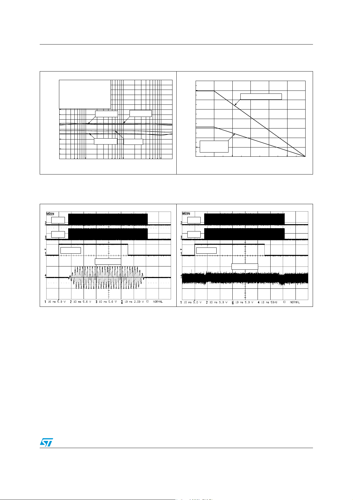
TS4999 Electrical characteristics
Figure 52. CMRR vs. frequency
(3D effect on)
0
Vcc = 2.5V, 3D effect on
Δ
Vic = 200mVpp
-10
Cin = 10μF
RL = 8Ω +≥ 15μH
-20
Tamb = 25°C
-30
-40
-50
CMRR(dB)
-60
-70
-80
20
G=+9.5dB
G=+3.5dB
100 1000 10000
Frequency (Hz)
G=+12dB
G=+6dB
Figure 54. Startup and shutdown phase
V
= 5 V, G= 6 dB, Cin=1µF,
CC
V
=2Vpp, F= 500 Hz
in
Out+
Figure 53. Power derating curves
1.6
1.4
1.2
1.0
0.8
0.6
0.4
No Heat sink
0.2
AMR value
Flip-Chip Package Power Dissipation (W)
0.0
0 255075100125150
Ambiant Temperature (°C)
With a 4-layer PCB
Figure 55. Startup and shutdown phase
=5V, G=6dB, Cin= 1 µF, inputs
V
CC
grounded
Out+
Out-
Standby
Out-
Standby
Out+ - Out-
Out+ - Out-
23/36
Page 24
Application information TS4999
4 Application information
4.1 Differential configuration principle
The TS4999 is a monolithic fully-differential input/output class D stereo power amplifier. The
TS4999 also features 3D effect enhancement that can be switched on or off by one digital
pin. Additionally, since the load is connected differentially compared to a single-ended
topology, the output is four times higher for the same power supply voltage.
A fully-differential amplifier offers the following advantages.
● A high PSRR (power supply rejection ratio).
● A high common mode noise rejection.
● Virtually zero pop with no additional circuitry, giving a faster start-up time compared to
conventional single-ended input amplifiers.
● Easier interfacing with differential output audio DACs.
4.2 Gain settings
In the flat region of the frequency-response curve (no input coupling capacitor or internal
feedback loop + load effect), the differential gain can be set to 3.5, 6, 9.5 or 12 dB,
depending on the logic level of the G0 and G1 pins, as shown in Tab l e 1 1 .
Table 11. Gain settings with G0 and G1 pins
G1 G0 Gain (dB) Gain (V/V)
003.51.5
0162
109.53
11124
Note: Between pins G0, G1 and GND there is an internal 300 kΩ (+/-20%) resistor. When the pins
are floating, the gain is 6 dB. In full standby (left and right channels OFF), these resistors
are disconnected (HiZ input).
4.3 3D effect enhancement
The TS4999 features 3D audio effects which can be switched off and switched on through
input pin 3D when used as a digital interface. The relation between the logic level of this pin
and the on/off 3D effect is shown in Table 3 on page 4 and Table 7 on page 6.
The 3D audio effect evokes the perception of spatial hearing of stereo audio signals and
improves this effect in cases where the stereo speakers are too close to each other, such as
in small or portable devices.
The perceived amount of 3D effect also depends on many factors such as speaker position,
distance between speakers, listener/frequency spectrum of the audio signal, as well as the
difference of signal between the left and right channel.
24/36
Page 25
TS4999 Application information
In some cases, the speaker volume can increase when the 3D effect is switched on. This
factor is dependent on the composition and frequency spectrum of listened stereo audio
signal.
Note: 1 When the 3D effect is switched on, both channels must be in operation or shutdown mode at
the same time.
2 Between pin 3D and GND there is an internal 300 k
Ω
(+/-20%) resistor. When the pin is
floating, the 3D effect is off. In full standby (left and right channels OFF), this resistor is
disconnected (HiZ input).
4.4 Low frequency response
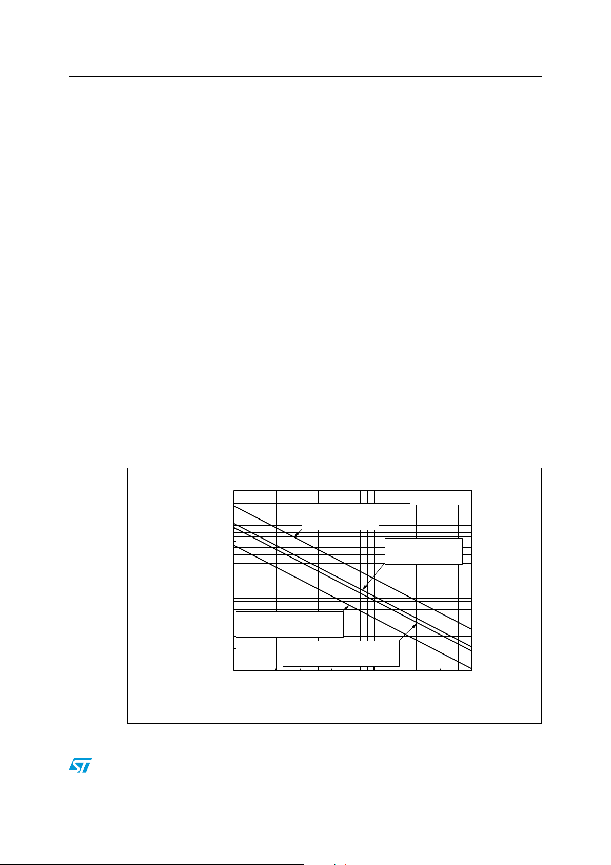
If a low frequency bandwidth limitation is required, input coupling capacitors can be used. In
the low frequency region, the input coupling capacitor C
with the input impedance Z
, a first order high-pass filter with a -3 dB cut-off frequency.
in
--------------------------------------------=
F
CL
2 π Z
1
⋅⋅ ⋅
inCin
starts to have an effect. Cin forms,
in
So, for a desired cut-off frequency F
with F
The input impedance Z
in Hz, Zin in Ω and Cin in F.
CL
is for the whole power supply voltage range and changes with the
in
C
CL
in
, C
is calculated as follows:
in
--------------------------------------------- -=
2 π Z
1
⋅⋅ ⋅
inFCL
gain setting. There is also a tolerance around the typical values (see Ta bl e 8 , Table 9 and
Ta bl e 1 0.
Figure 56. Cut-off frequency vs. input capacitor
Tamb=25°C
G=12dB, 3D on
100
10
G=3.5dB, 6dB, 9.5dB
3D off, Zin=30kΩ typ.
Zin=8.6kΩ typ.
G=12dB, 3D off
Zin=15kΩ typ.
Low -3dB Cut Off Frequency (Hz)
1
0.1 1
G=3.5dB, 6dB, 9.5dB
3D on, Zin=17.1kΩ typ.
Input Capacitor Cin (μF)
25/36
Page 26

Application information TS4999
4.5 Circuit decoupling
Power supply capacitors, referred to as CS, C
TS4999.
The TS4999 has a typical switching frequency of 280 kHz and an output fall and rise time of
approximately 5 ns. Due to these very fast transients, careful decoupling is mandatory.
A 1 µF ceramic capacitor between each PVCC and PGND (C
ceramic capacitor between AVCC and AGND 0.1 µF (C
located as close as possible to the TS4999 in order to avoid any extra parasitic inductance
or resistance created by a long track wire. Parasitic loop inductance, in relation to di/dt,
introduces overvoltage that decreases the global efficiency of the device and may cause, if
this parasitic inductance is too high, the device to break down.
In addition, even if a ceramic capacitor has an adequate high frequency ESR (equivalent
series resistance) value, its current capability is also important. A 0603 size is a good
compromise, particularly when a 4 Ω load is used.
Another important parameter is the rated voltage of the capacitor. A 1 µF/6.3 V capacitor
used at 5 V, loses about 50% of its value. With a power supply voltage of 5 V, the decoupling
value, instead of 1 µF, could be reduced to 0.5 µF. As C
THD+N in the medium-to-high frequency region, this capacitor variation becomes decisive.
In addition, less decoupling means higher overshoots which can be problematic if they reach
the power supply AMR value (6 V).
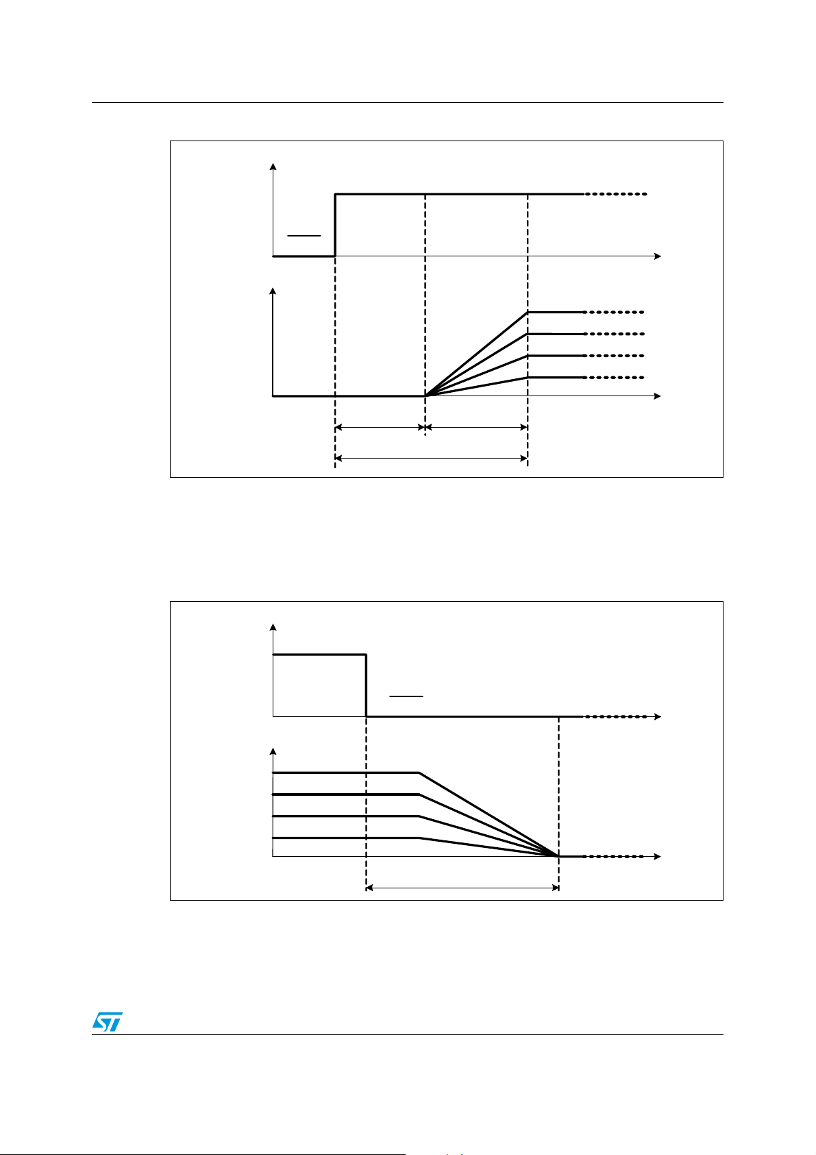
4.6 Wakeup (tWU) and shutdown (t
During the wake-up sequence, there is a delay when the standby is released to switch the
device ON. The wake-up sequence of the TS4999 consists of two phases. During the first
phase t
phase t
selected by the digital pins G0 and G1. This startup sequence avoid any pop noise during
startup of the amplifier. See Figure 57: Wake-up phase
, a digitally-generated delay, mutes the outputs. Then, the gain increasing-
WU-A
begins. The gain increases smoothly from the mute state to the preset gain
WU-A
and CSR, are needed to correctly bypass the
SL
, CSR) and one additional
SL
) are sufficient, but they must be
S
has particular influence on the
S
) times
STBY
26/36
Page 27
TS4999 Application information
Figure 57. Wake-up phase
STBY
Level
HI
LO
STBY
STBY
Time
Preset gainGain increasing
Gain
Mute
Mute
t
WU-A
t
WU
t
WU-B
Time
When the standby command is set, the time required to set the output stage to high
impedance and to put the internal circuitry in shutdown mode is called the standby time.
This time is used to decrease the gain from its nominal value set by the digital pins G0 and
G1 to mute and avoid any pop noise during shutdown. The gain decreases smoothly until
the outputs are muted. See Figure 58: Shutdown phase.
Figure 58. Shutdown phase
STBY
Level
HI
LO
STBY
STBY
Time
Gain
Preset gain
Gain decreasing
Mute
Mute
t
STBY
27/36
Time
Page 28
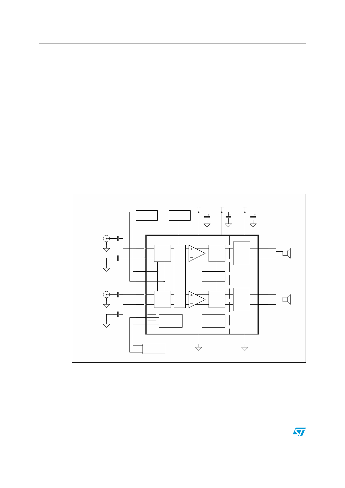
Application information TS4999
4.7 Consumption in shutdown mode
Between the shutdown pin and GND there is an internal 300 kΩ (+-/20%) resistor. This
resistor forces the TS4999 to be in shutdown mode when the shutdown input is left floating.
However, this resistor also introduces additional shutdown power consumption if the
shutdown pin voltage is not at 0 V.
With a 0.4 V shutdown voltage pin for example, you must add 0.4 V/300 kΩ = 1.3 µA typical
(0.4 V/240 kΩ = 1.66 µA in maximum) for each shutdown pin to the standby current
specified in Ta ble 8, Table 9 and Tab l e 1 0 .
Of course, this current will be provided by the external control device for standby pins.
4.8 Single-ended input configuration
It is possible to use the TS4999 in a single-ended input configuration. Input coupling
capacitors are also mandatory in this configuration. The schematic diagram in Figure 59
shows a typical single-ended input application.
Figure 59. Typical single-ended input application
Le ft Inp ut
Right Input
LPVCC
H
Bridge
VCC
CsL
1uF
B6
A5
Lout+
A7
Lout-
Left spea ker
Cs
VCC VCC
0.1uF
Gain Select
Contro l
TS4999
Cin
Cin
Lin+
A1
Lin-
B2
G0
C3
G1
C5
Gain
Select
3D Effect
Contro l
C13D
D4
AVCC
Osci llator
PWM
D6
RPVCC
CsR
1uF
3D EFFECT
Rin+
E1
Cin
Cin
D2
A3
E3
Gain
Select
Rin-
STBYL
STBYR
Standby Control
Standby
Control
PWM
Protection
Circuit
B4
H
Bridge
PGNDAGND
Rout+
E5
Rout-
E7
Right speaker
C7
28/36
Page 29
TS4999 Application information
4.9 Output filter considerations
The TS4999 is designed to operate without an output filter. However, due to very sharp
transients on the TS4999 output, EMI-radiated emissions may cause some standard
compliance issues.
These EMI standard compliance issues can appear if the distance between the TS4999
outputs and loudspeaker terminal are long (typically more than 50 mm, or 100 mm in both
directions, to the speaker terminals). Because the PCB layout and internal equipment
device are different for each configuration, it is difficult to provide a one-size-fits-all solution.
However, to decrease the probability of EMI issues, there are several simple rules to follow.
● Reduce, as much as possible, the distance between the TS4999 output pins and the
speaker terminals.
● Use a ground plane for "shielding" sensitive wires.
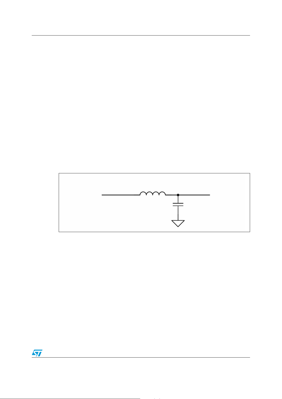
● Place, as close as possible to the TS4999 and in series with each output, a ferrite bead
with a rated current of at least 2.5 A and impedance greater than 50-Ω at frequencies
above 30 MHz. If, after testing, these ferrite beads are not necessary, replace them by
a short-circuit.
● Allow extra footprint to place, if necessary, a capacitor to short perturbations to ground
(see Figure 60).
Figure 60. Ferrite chip bead placement
From output
Ferrite chip bead
to speaker
about 100pF
gnd
In the case where the distance between the TS4999 output and the speaker terminals is too
long, it is possible to encounter low frequency EMI issues due to the fact that the typical
operating PWM frequency is 280 kHz and that the fall and rise time of the output signal is
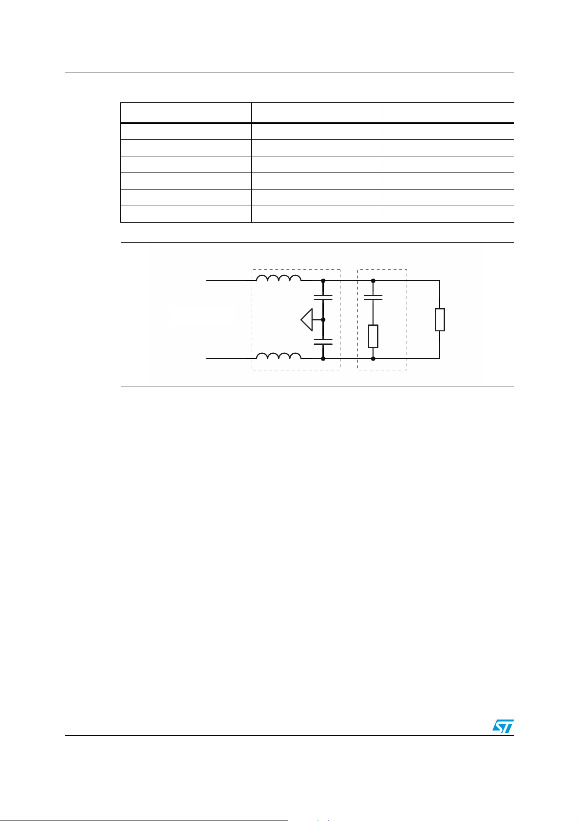
less than or equal to 5 ns. In this configuration, it is necessary to use the output filter
represented in Figure 61 on page 30, which consists of L1, C1, L2 and C2 being placed as
close as possible to the TS4999 outputs.
In particular cases where the output filter is used and there is the possibility to disconnect a
load, we recommended using an RC network that consists of C3 and R, as shown in
Figure 61. In this case, when the output filter is connected without any load, the filter acts as
a short-circuit for frequencies above 10 kHz in the output frequency spectrum of the
amplifier. The RC network corrects the frequency response of the output filter and
compensates this limitation.
29/36
Page 30
Application information TS4999
Table 12. Example of component selection
Component RL = 4 Ω RL = 8 Ω
L1 15μH / 1.4A 30μH / 0.7A
L2 15μH / 1.4A 30μH / 0.7A
C1 2μF / 10V 1μF / 10V
C2 2μF / 10V 1μF / 10V
C3 1μF / 10V 1μF / 10V
R22Ω / 0.25W 47Ω / 0.25W
Figure 61. LC output filter with RC network
LC Output Filter
OUT+
from TS2007
OUT-
4.10 Short-circuit protection
The TS4999 includes an output short-circuit protection. This protection prevents the device
from being damaged when faults occur on the amplifier outputs.
When a channel is in operating mode and a short-circuit occurs between two outputs of the
channel or between an output and ground, the short-circuit protection detects this situation
and puts the appropriate channel into standby mode. To put the channel back into operating
mode, it is necessary to put the channel’s standby pin to logical LO and then back to logical
HI and wake-up the channel.
L1
L2
C1
C2
RC network
C3
R
R
L
4.11 Thermal shutdown
The TS4999 device has an internal thermal shutdown protection mechanism to protect the
device from overheating in the event of extreme temperatures. The thermal shutdown
mechanism is activated when the device reaches 150° C. When the temperature decreases
to safe levels (around 135° C), the circuit switches back to normal operation.
30/36
Page 31
TS4999 Package mechanical data
5 Package mechanical data
In order to meet environmental requirements, ST offers these devices in different grades of
ECOPACK® packages, depending on their level of environmental compliance. ECOPACK®
specifications, grade definitions and product status are available at: www.st.com.
ECOPACK® is an ST trademark.
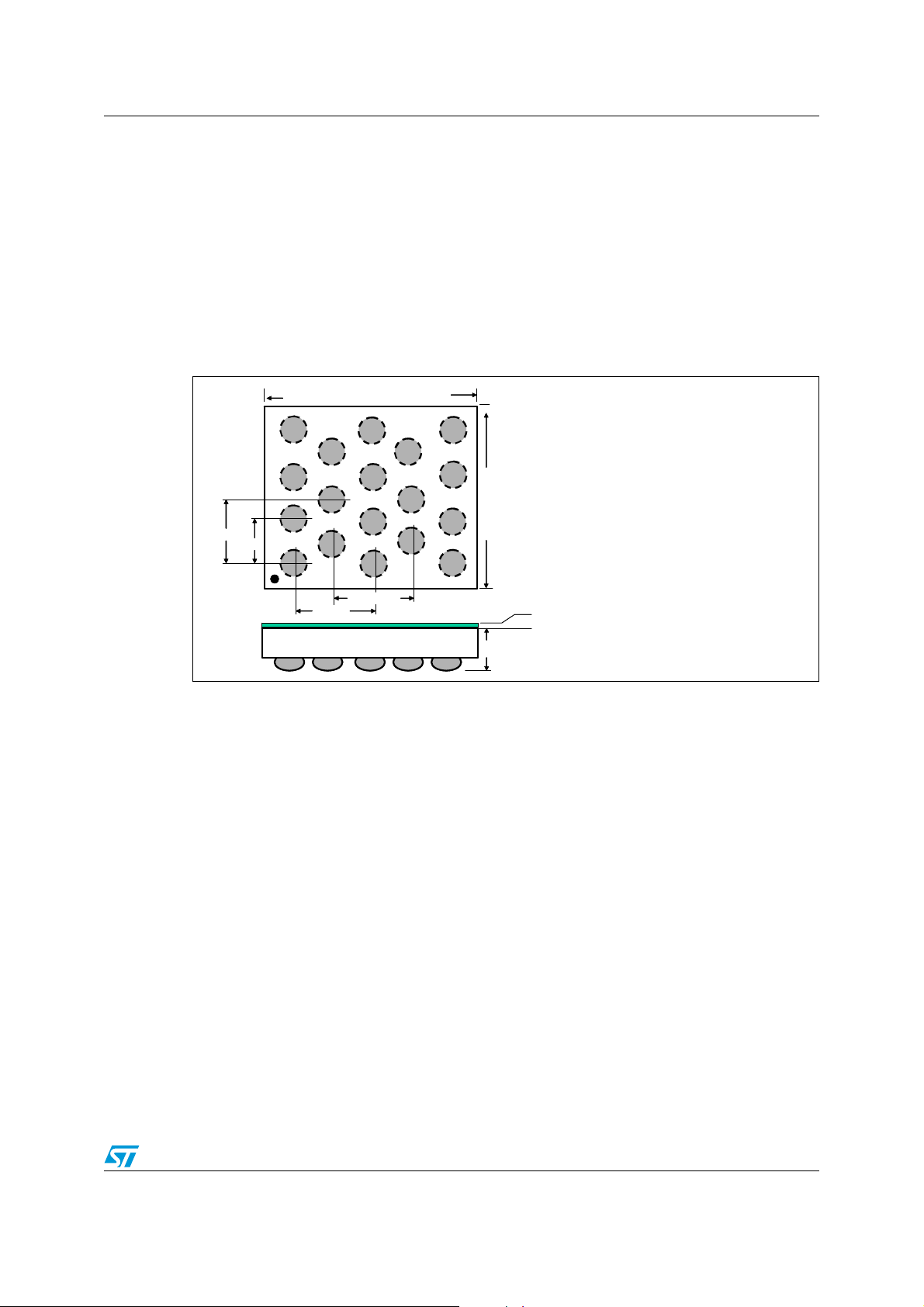
5.1 Flip chip package
Figure 62. Flip chip package
2420 μm
2420 μm
Die size: 2.42x2.28 mm ± 100µm
Die height (including bumps): 600µm
Bumps diameter: 315µm ±50µm
2280 μm
750μm
750μm
500μm
500μm
866μm
866μm
866μm
866μm
2280 μm
600 μm
600 μm
Bump diameter before reflow: 300µm ±10µm
Bumps height: 250µm ±40µm
Die height: 350µm ±20µm
Pitch: 500µm ±50µm
Coplanarity: 50µm max
Optional*: Back coating height: 40µm
40 μm*
40 μm*
31/36
Page 32
Package mechanical data TS4999
Figure 63. Pinout (top view)
7
LOUT-
6
5
LOUT+
4
3
STDBYL
2
1
LIN+
AEDCB
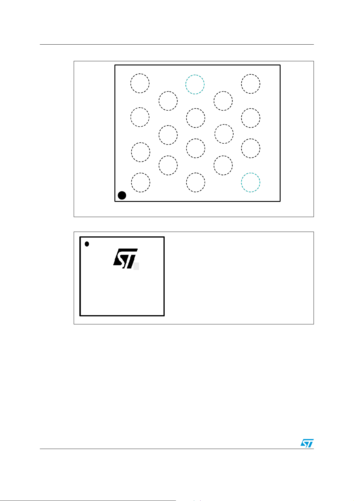
Figure 64. Marking (top view)
E
E
K9 X
K9 X
YWW
YWW
PGND
LPVCC
G1
AGND
G0
LIN- RIN-
■ ST Logo
■ Symbol for lead-free: E
■ Two first product code: K9
■ third X: Assembly Line Plant code
■ Three digits date code: Y for year - WW for week
■ The dot is for marking pin A1
RPVCC
AVCC
ROUT-
ROUT+
STDBYR
RIN+3D
32/36
Page 33
TS4999 Package mechanical data
5.2 Tape and reel package
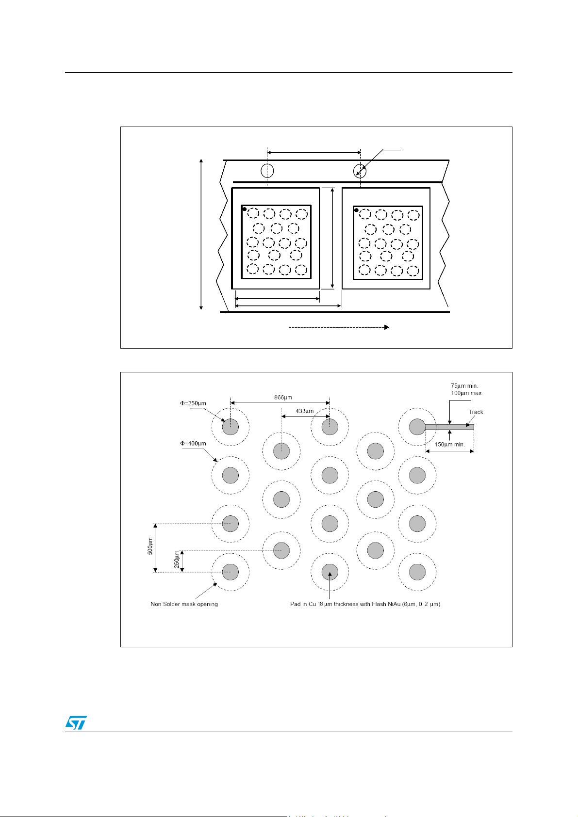
Figure 65. Schematic (top view)
1.5
4
4
1
11
A
A
8
8
Die size X + 70µm
Die size X + 70µm
4
4
All dimensions are in mm
All dimensions are in mm
User direction of feed
User direction of feed
A
A
Die size Y + 70µm
Die size Y + 70µm
1.5
1
11
Figure 66. Recommended footprint data
33/36
Page 34

Ordering information TS4999
6 Ordering information
Table 13. Order codes
Part number
TS4999EIJT -40°C to +85°C Flip chip 18 Tape & reel K9
Temperature
range
Package Packing Marking
34/36
Page 35

TS4999 Revision history
7 Revision history
Table 14. Document revision history
Date Revision Changes
18-Dec-2008 1 Initial release.
35/36
Page 36

TS4999
Please Read Carefully:
Information in this document is provided solely in connection with ST products. STMicroelectronics NV and its subsidiaries (“ST”) reserve the
right to make changes, corrections, modifications or improvements, to this document, and the products and services described herein at any
time, without notice.
All ST products are sold pursuant to ST’s terms and conditions of sale.
Purchasers are solely responsible for the choice, selection and use of the ST products and services described herein, and ST assumes no
liability whatsoever relating to the choice, selection or use of the ST products and services described herein.
No license, express or implied, by estoppel or otherwise, to any intellectual property rights is granted under this document. If any part of this
document refers to any third party products or services it shall not be deemed a license grant by ST for the use of such third party products
or services, or any intellectual property contained therein or considered as a warranty covering the use in any manner whatsoever of such
third party products or services or any intellectual property contained therein.
UNLESS OTHERWISE SET FORTH IN ST’S TERMS AND CONDITIONS OF SALE ST DISCLAIMS ANY EXPRESS OR IMPLIED
WARRANTY WITH RESPECT TO THE USE AND/OR SALE OF ST PRODUCTS INCLUDING WITHOUT LIMITATION IMPLIED
WARRANTIES OF MERCHANTABILITY, FITNESS FOR A PARTICULAR PURPOSE (AND THEIR EQUIVALENTS UNDER THE LAWS
OF ANY JURISDICTION), OR INFRINGEMENT OF ANY PATENT, COPYRIGHT OR OTHER INTELLECTUAL PROPERTY RIGHT.
UNLESS EXPRESSLY APPROVED IN WRITING BY AN AUTHORIZED ST REPRESENTATIVE, ST PRODUCTS ARE NOT
RECOMMENDED, AUTHORIZED OR WARRANTED FOR USE IN MILITARY, AIR CRAFT, SPACE, LIFE SAVING, OR LIFE SUSTAINING
APPLICATIONS, NOR IN PRODUCTS OR SYSTEMS WHERE FAILURE OR MALFUNCTION MAY RESULT IN PERSONAL INJURY,
DEATH, OR SEVERE PROPERTY OR ENVIRONMENTAL DAMAGE. ST PRODUCTS WHICH ARE NOT SPECIFIED AS "AUTOMOTIVE
GRADE" MAY ONLY BE USED IN AUTOMOTIVE APPLICATIONS AT USER’S OWN RISK.
Resale of ST products with provisions different from the statements and/or technical features set forth in this document shall immediately void
any warranty granted by ST for the ST product or service described herein and shall not create or extend in any manner whatsoever, any
liability of ST.
ST and the ST logo are trademarks or registered trademarks of ST in various countries.
Information in this document supersedes and replaces all information previously supplied.
The ST logo is a registered trademark of STMicroelectronics. All other names are the property of their respective owners.
© 2008 STMicroelectronics - All rights reserved
STMicroelectronics group of companies
Australia - Belgium - Brazil - Canada - China - Czech Republic - Finland - France - Germany - Hong Kong - India - Israel - Italy - Japan -
Malaysia - Malta - Morocco - Singapore - Spain - Sweden - Switzerland - United Kingdom - United States of America
www.st.com
36/36
 Loading...