

Page 1
Precision low noise dual operational amplifier
Features
■ Large output voltage swing
+14.3V/-14.6 V
■ Low input offset voltage 850 μV max.
■ Low voltage noise: 4.5 nV/√Hz
■ High gain bandwidth product: 15 MHz
■ High slew rate: 7 V/μs
■ Low distortion: 0.002 %
■ ESD internal protection 2 kV
■ Excellent frequency stability
■ Macromodel included in this specification
Description
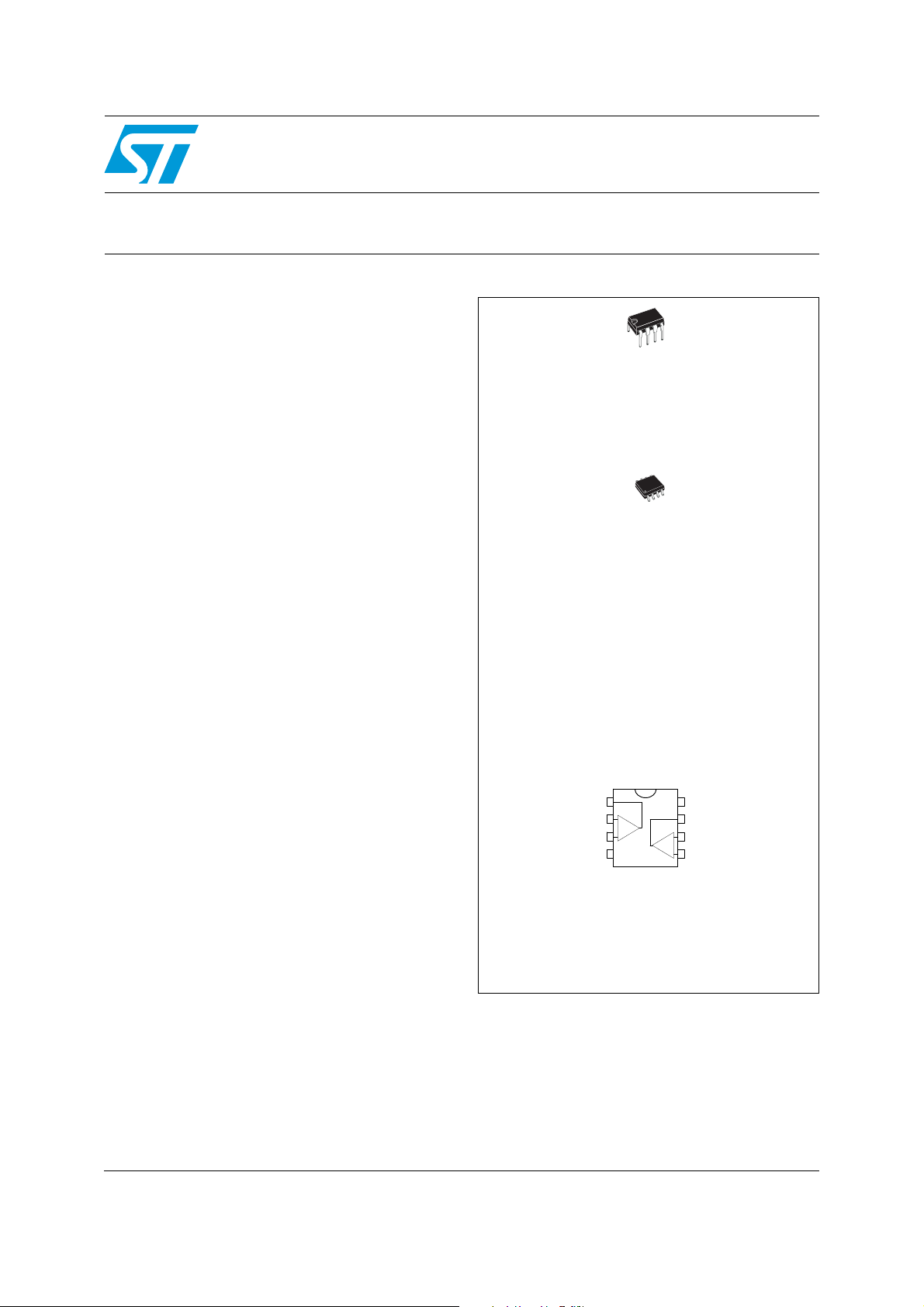
TS522
N
DIP8
(Plastic Package)
D
SO8
(Plastic Micropackage)
The TS522 is a monolithic dual operational
amplifier mainly dedicated to audio applications.
The TS522 offers a very low input offset voltage
as well as low voltage noise (4.5 nV/√Hz) and
high dynamic performances (15 MHz gain
bandwidth product, 7 V/μs slew rate).
The output stage allows a large output voltage
swing and symmetrical source and sink currents.
Output 1
Inverting input 1
Non-inverting input 1
V
Pin connections
top view
+
-
+
V
8
CC
Output 2
7
6
Inverting input 2
Non-inverting input 2
1
2
-
+
3
-
45
CC
October 2008 Rev 2 1/13
www.st.com
13
Page 2
Absolute maximum ratings and operating conditions TS522
1 Absolute maximum ratings and operating conditions
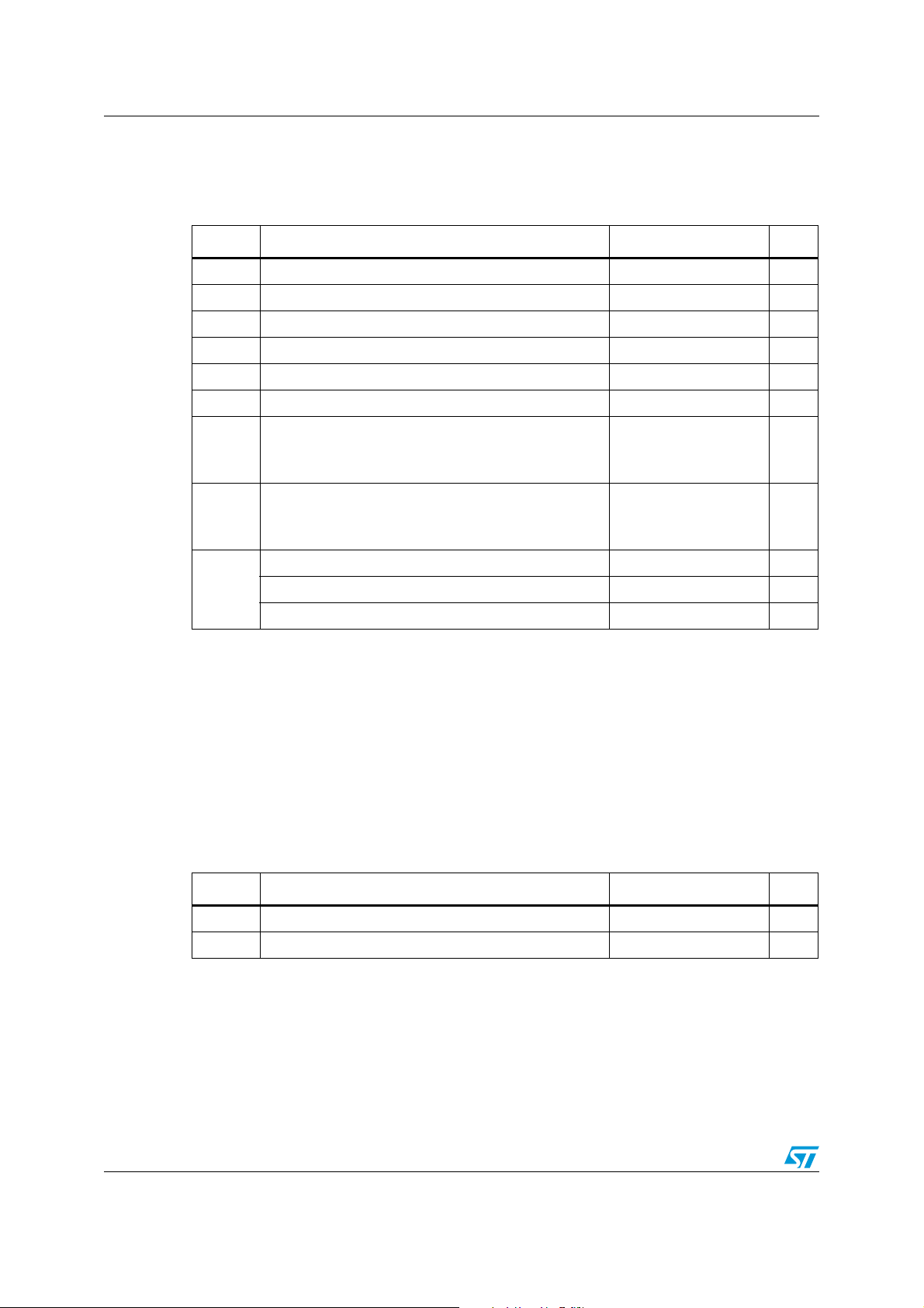
Table 1. Absolute maximum ratings
Symbol Parameter Value Unit
V
V
T
R
R
ESD
1. Either or both input voltages must not exceed the magnitude of V
2. Power dissipation must be considered to ensure maximum junction temperature (Tj) is not exceeded.
3. Short-circuits can cause excessive heating and destructive dissipation.
4. R
5. Human body model: a 100 pF capacitor is charged to the specified voltage, then discharged through a
1.5 kΩ resistor between two pins of the device. This is done for all couples of connected pin combinations
while the other pins are floating.
6. Machine model: a 200 pF capacitor is charged to the specified voltage, then discharged directly between
two pins of the device with no external series resistor (internal resistor < 5 Ω). This is done for all couples of
connected pin combinations while the other pins are floating.
7. Charged device model: all pins and the package are charged together to the specified voltage and then
discharged directly to the ground through only one pin. This is done for all pins.
Table 2. Operating conditions
Supply voltage ±18 to 36 V
CC
(6)
(1)
(5)
(2)
(7)
(3) (4)
(3) (4)
CC
+
or V
CC
±30 V
±15 V
Infinite
125
85
40
41
2kV
200 V
1.5 kV
-
Differential input voltage
id
V
i
Input voltage
(1)
Output short-circuit duration
T
Maximum junction temperature + 150 °C
j
Storage temperature range -65 to +150 °C
stg
Thermal resistance junction to ambient
thja
SO-8
DIP8
Thermal resistance junction to case
thjc
SO-8
DIP8
HBM: human body model
MM: machine model
CDM: charged device model
are typical values.
th
°C/W
°C/W
Symbol Parameter Value Unit
V
T
Supply voltage ±2.5 to ±15 V
CC
Operating free-air temperature range -40 to 125 °C
oper
2/13
Page 3
TS522 Schematic diagram
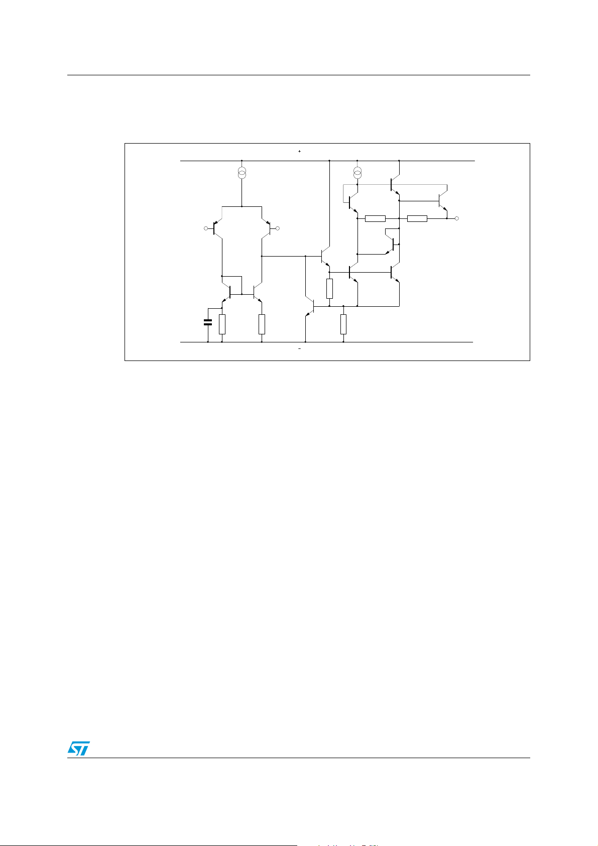
2 Schematic diagram
Figure 1. Typical schematic diagram (1/2 TS522)
V
CC
Inverting
Input
Non-inverting
Input
V
CC
Output
3/13
Page 4
Electrical characteristics TS522
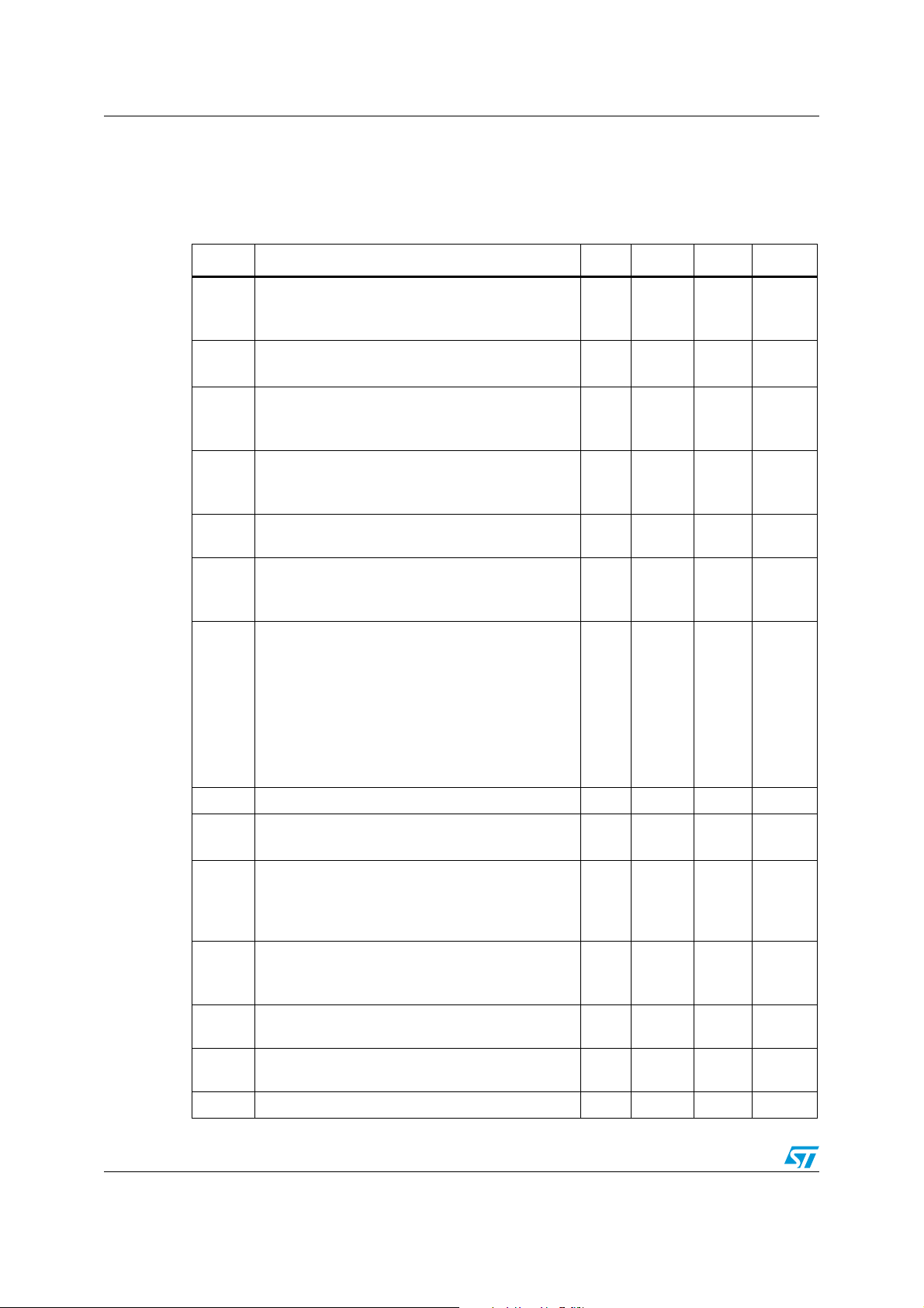
3 Electrical characteristics
Table 3. VCC+ = 15 V, VCC- = -15 V, T
(unless otherwise specified)
Symbol Parameter Min. Typ. Max. Unit
amb
= 25° C
V
ΔV
Iio
I
ib
Vicm
A
±V
Input offset voltage (Vo = 0V, Vic = 0V)
io
io
amb
T
≤ T
amb
≤ T
max
min
Input offset voltage drift
Vic = 0V, Vo = 0V, T
min
Input offset current (V
T
= +25°C
amb
≤ T
amb
≤ T
max
T
min
≤ T
≤ T
amb
= 0V, Vo = 0V)
ic
max
= +25°C
T
Input bias current (Vic = 0V, Vo = 0V)
= +25°C
T
amb
T
≤ T
≤ T
min
amb
max
Common mode input voltage range
(ΔV
= 5mV, Vo = 0V) ±13 ±14 V
io
Large signal voltage gain (RL = 2kΩ, Vo = ±10V)
= +25°C
vd
T
T
amb
min
≤ T
amb
≤ T
max
Output voltage swing (Vid = ±1V)
RL = 600Ω
= 600Ω
R
L
opp
RL = 2.0kΩ
= 2.0kΩ
R
L
90
85
13.2
0.85
1.7
2
10 150
175
250 750
800
100
12.2
-12.7
14
-14.2
-13.2
mV
μV/°C
nA
nA
dB
V
RL = 10kΩ
= 10kΩ
R
L
CMR Common mode rejection ratio (V
SVR
Supply voltage rejection ratio
+
Vcc
/Vcc- = +15V/-15V to +5V/-5V 80 105
Output short circuit current
= ±1V, Output to ground)
(V
I
o
id
Source
Sink
Supply current (Vo = 0V, all amplifiers)
I
cc
SR
GBP
= +25°C
T
amb
T
≤ T
≤ T
min
amb
max
Slew rate
= -10V to +10V, RL = 2kΩ, CL = 100pF, AV = +1) 5 7 V/μs
(V
i
Gain bandwidth product
(f = 100kHz, R
= 2kΩ, CL = 100pF) 10 15 MHz
L
B Unity gain bandwidth (open loop) 9 MHz
4/13
13.5
= ±13V) 80 100 dB
ic
15
20
14.3
-14.6
29
37
-14
45
5.5
dB
mA
mA
Page 5
TS522 Electrical characteristics
Table 3. VCC+ = 15 V, VCC- = -15 V, T
amb
= 25° C
(unless otherwise specified) (continued)
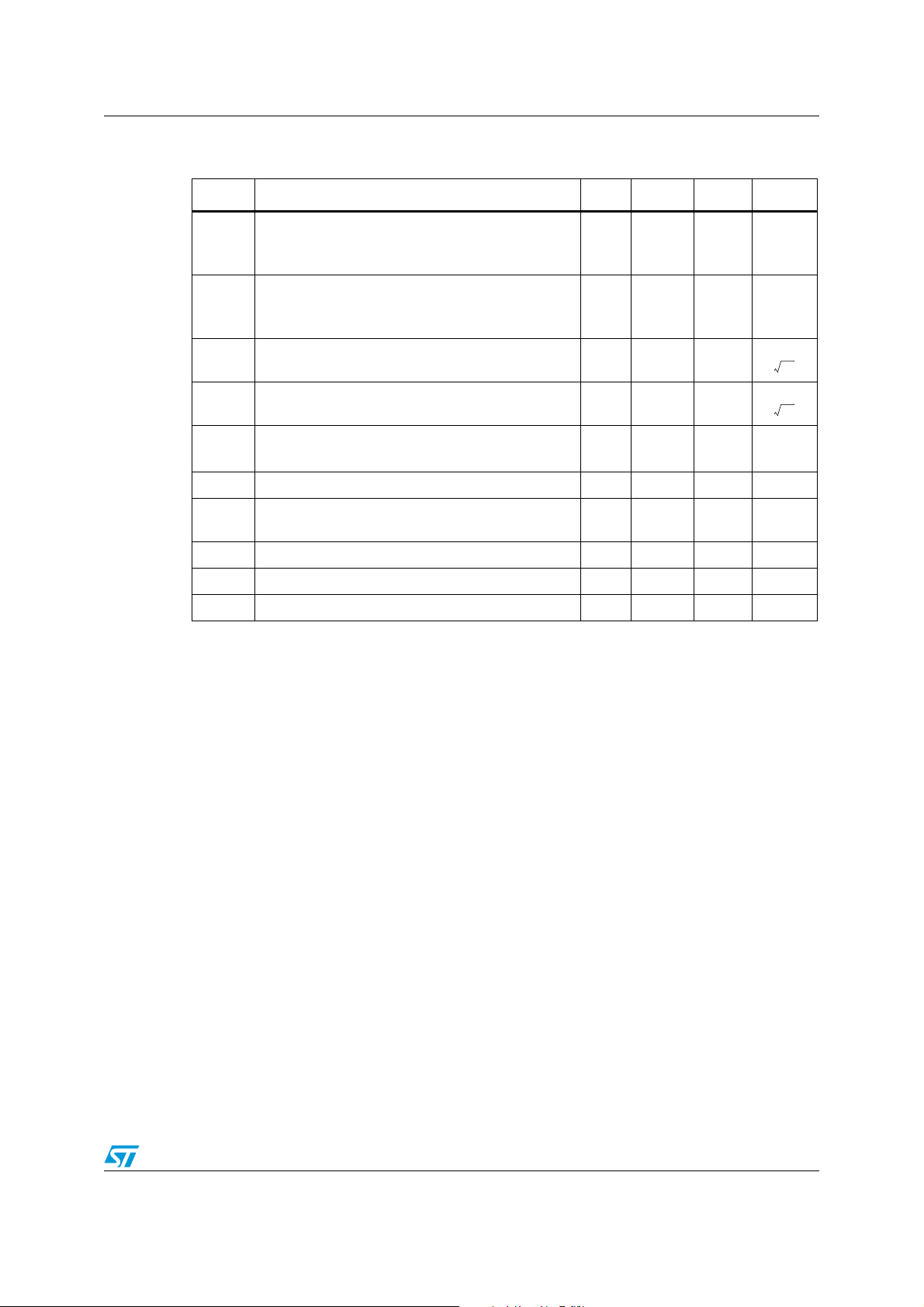
Symbol Parameter Min. Typ. Max. Unit
Gain margin (RL = 2kΩ)
A
∅m
THD
V
o1/Vo2
FPB
m
e
n
i
n
Z
o
R
i
C
i
= 0pF
C
L
CL = 100pF
-11
-6
Phase margin
= 0pF
C
L
= 100pF
C
L
Equivalent input noise voltage
(Rs = 100Ω, f = 1kHz)
Equivalent input noise current
(f = 1kHz)
55
30
4.5
0.5
Degrees
------------
------------
Total harmonic distortion
= 2kΩ, f = 20Hz to 20kHz, Vo = 3V
R
L
, Av = +1 0.002
rms
Channel separation (f = 20Hz to 20kHz) 120 dB
Full power bandwidth
= 27Vpp, RL = 2kΩ, THD ≤ 1%)
(V
o
120 kHz
Output impedance (Vo = 0V, f = 9MHz) 37 Ω
Input resistance (Vic = 0V) 175 kΩ
Input capacitance (Vic = 0V) 12 pF
dB
nV
Hz
pA
Hz
%
5/13
Page 6
Electrical characteristics TS522
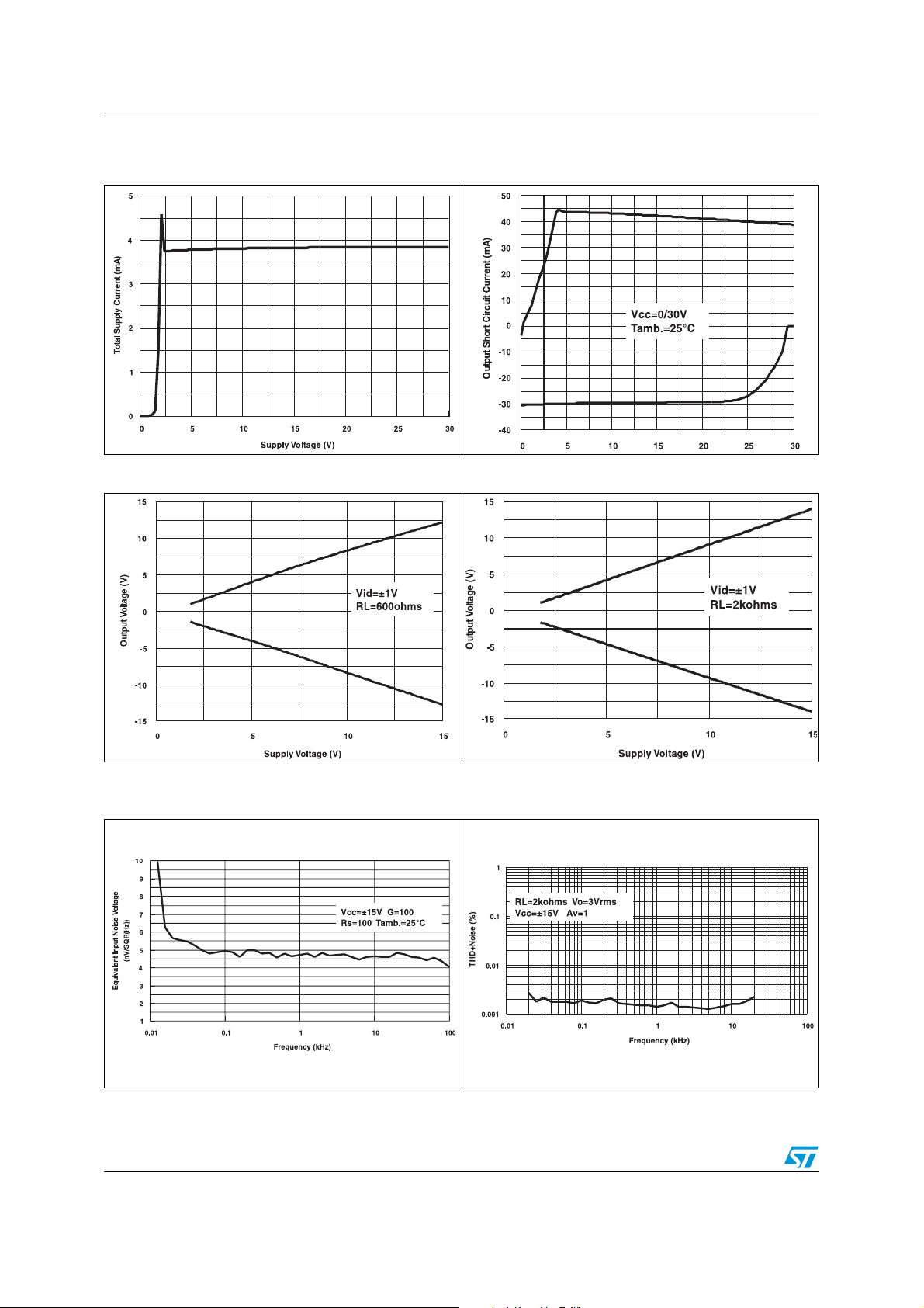
Figure 2. Total supply current vs supply
voltage
Figure 3. Output short circuit current vs
output voltage
Figure 4. Output voltage vs supply voltage Figure 5. Output voltage vs supply voltage
Figure 6. Equivalent input noise voltage vs
frequency
6/13
Figure 7. THD + Noise vs frequency
Page 7
TS522 Electrical characteristics
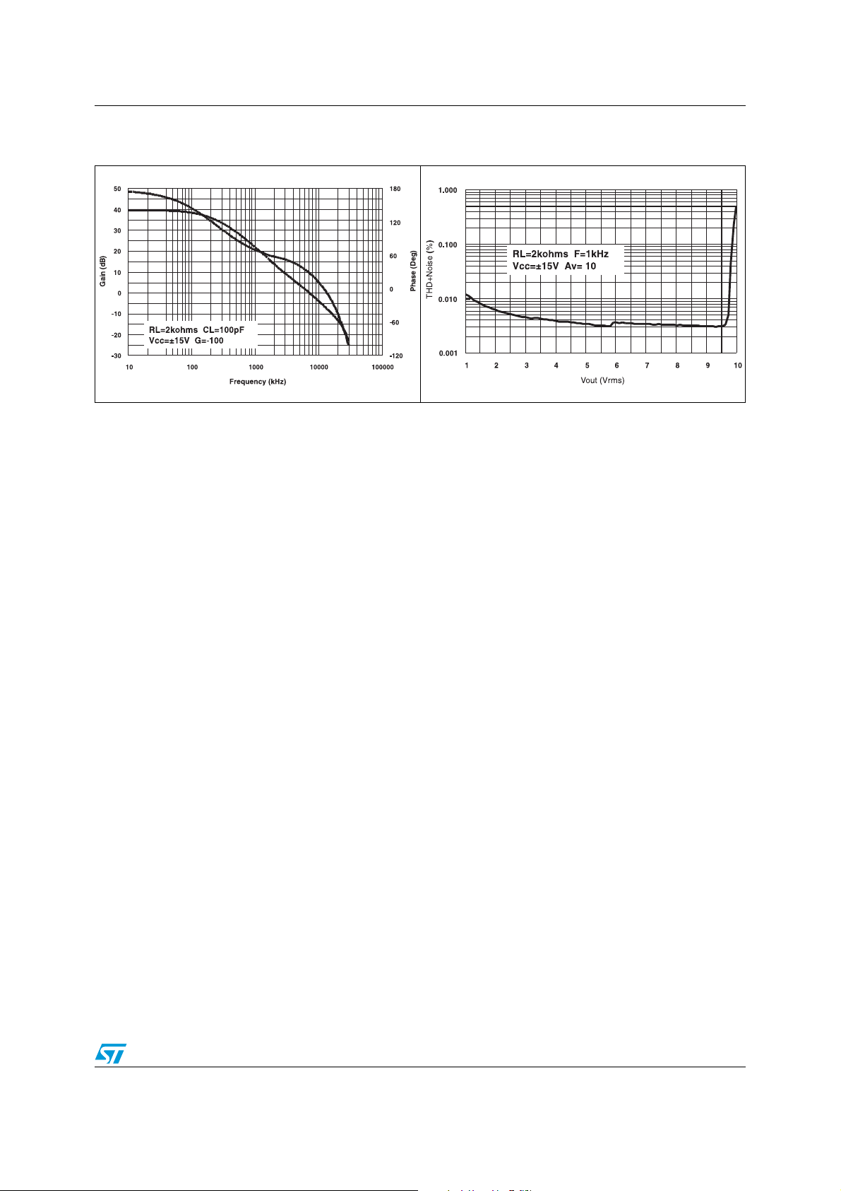
Figure 8. Voltage gain and phase vs
frequency
Figure 9. THD + Noise vs Vout
7/13
Page 8

Package information TS522
4 Package information
In order to meet environmental requirements, ST offers these devices in ECOPACK®
packages. These packages have a Lead-free second level interconnect. The category of
second level interconnect is marked on the package and on the inner box label, in
compliance with JEDEC Standard JESD97. The maximum ratings related to soldering
conditions are also marked on the inner box label. ECOPACK is an ST trademark.
ECOPACK specifications are available at: www.st.com
.
8/13
Page 9
TS522 Package information
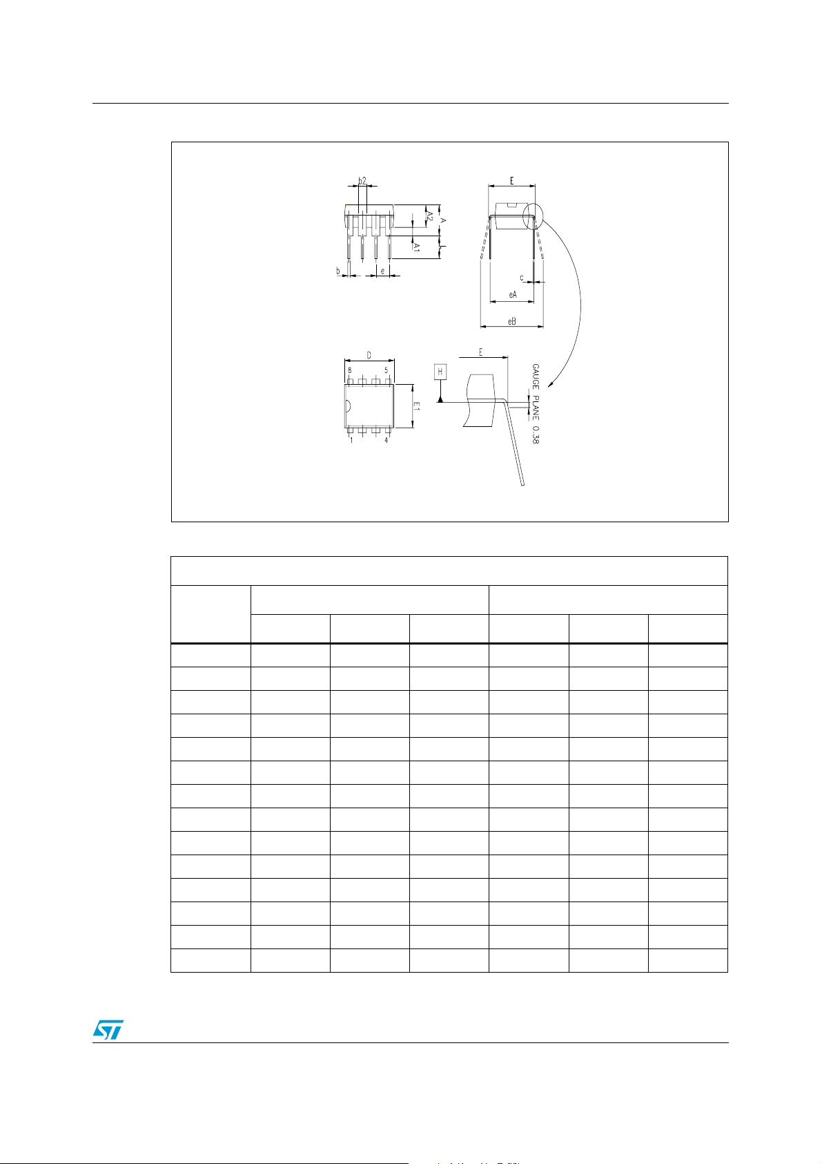
Figure 10. DIP8 package mechanical drawing
Table 4. DIP8 package mechanical data
Dimensions
Millimeters Inches
Ref.
Min. Typ. Max. Min. Typ. Max.
A 3.32 0.131
a1 0.51 0.020
B 1.15 1.65 0.045 0.065
b 0.356 0.55 0.014 0.022
b1 0.204 0.304 0.008 0.012
D 10.92 0.430
E 7.95 9.75 0.313 0.384
e 2.54 0.100
e3 7.62 0.300
e4 7.62 0.300
F 6.6 0260
i5.080.200
L 3.18 3.81 0.125 0.150
Z1.520.060
9/13
Page 10
Package information TS522
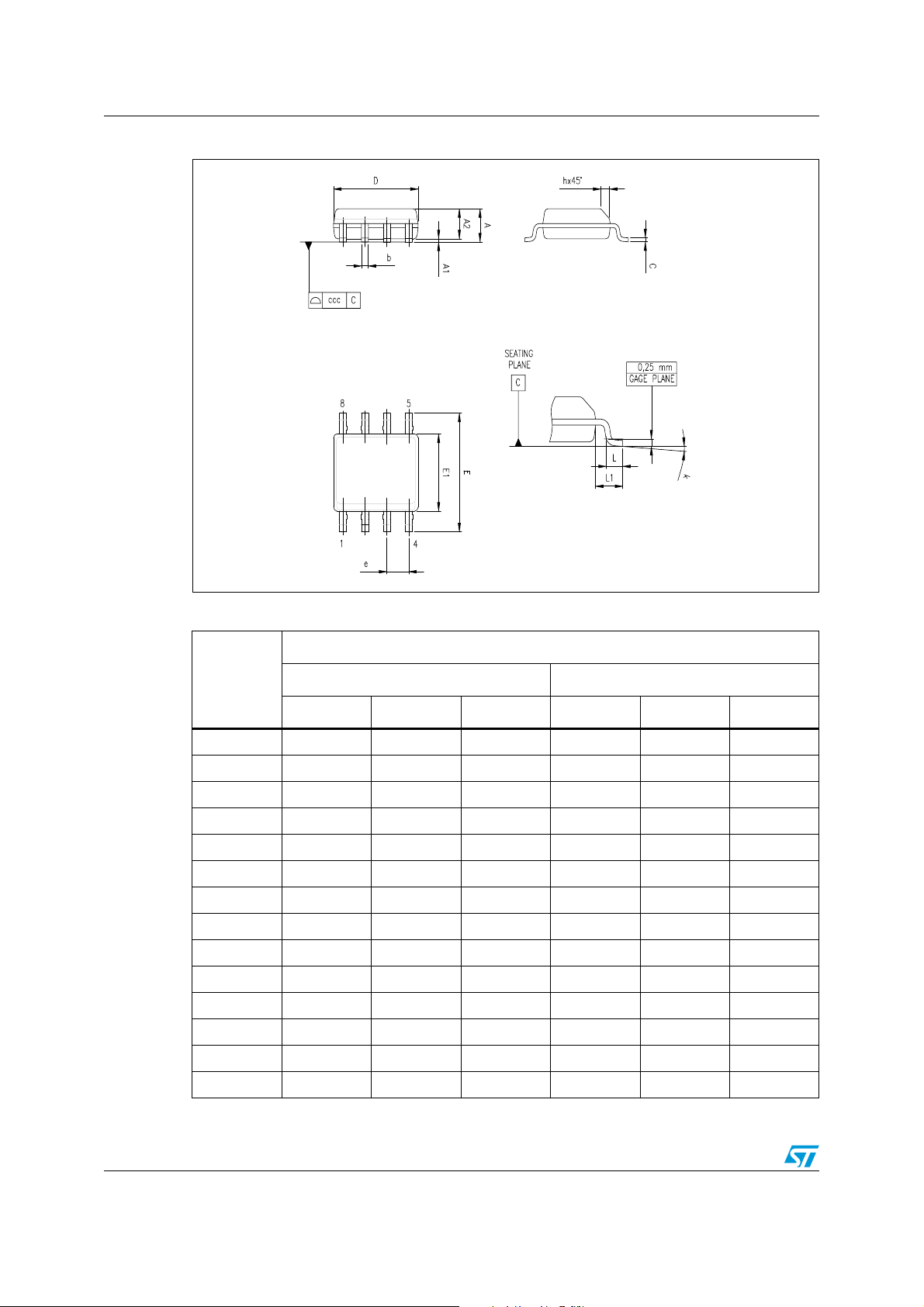
Figure 11. SO-8 package mechanical drawing
Table 5. SO-8 package mechanical data
Dimensions
Ref.
Millimeters Inches
Min. Typ. Max. Min. Typ. Max.
A1.750.069
A1 0.10 0.25 0.004 0.010
A2 1.25 0.049
b 0.28 0.48 0.011 0.019
c 0.17 0.23 0.007 0.010
D 4.80 4.90 5.00 0.189 0.193 0.197
E 5.80 6.00 6.20 0.228 0.236 0.244
E1 3.80 3.90 4.00 0.150 0.154 0.157
e 1.27 0.050
h 0.25 0.50 0.010 0.020
L 0.40 1.27 0.016 0.050
L1 1.04 0.040
k1° 8°1° 8°
ccc 0.10 0.004
10/13
Page 11
TS522 Ordering information
5 Ordering information
Table 6. Order codes
Order code
Temperature
range
Package Packing Marking
TS522ID/DT -40°C to +125°C SO-8 Tube/tape & reel 522I
TS522IN -40°C to +125°C DIP8 Tube TS522IN
TS522IYD/DT
1. Qualified and characterized according to AEC Q100 and Q003 or equivalent, advanced screening
according to AEC Q001 & Q 002 or equivalent.
(1)
-40°C to +125°C
SO-8
(Automotive grade)
Tube/tape & reel 522IY
11/13
Page 12
Revision history TS522
6 Revision history
Table 7. Document revision history
Date Revision Changes
01-Nov-2001 1 Initial release.
Document reformatted.
14-Oct-2008 2
Added automotive grade order codes in Table 6: Order codes.
Removed macromodel.
12/13
Page 13

TS522
Please Read Carefully:
Information in this document is provided solely in connection with ST products. STMicroelectronics NV and its subsidiaries (“ST”) reserve the
right to make changes, corrections, modifications or improvements, to this document, and the products and services described herein at any
time, without notice.
All ST products are sold pursuant to ST’s terms and conditions of sale.
Purchasers are solely responsible for the choice, selection and use of the ST products and services described herein, and ST assumes no
liability whatsoever relating to the choice, selection or use of the ST products and services described herein.
No license, express or implied, by estoppel or otherwise, to any intellectual property rights is granted under this document. If any part of this
document refers to any third party products or services it shall not be deemed a license grant by ST for the use of such third party products
or services, or any intellectual property contained therein or considered as a warranty covering the use in any manner whatsoever of such
third party products or services or any intellectual property contained therein.
UNLESS OTHERWISE SET FORTH IN ST’S TERMS AND CONDITIONS OF SALE ST DISCLAIMS ANY EXPRESS OR IMPLIED
WARRANTY WITH RESPECT TO THE USE AND/OR SALE OF ST PRODUCTS INCLUDING WITHOUT LIMITATION IMPLIED
WARRANTIES OF MERCHANTABILITY, FITNESS FOR A PARTICULAR PURPOSE (AND THEIR EQUIVALENTS UNDER THE LAWS
OF ANY JURISDICTION), OR INFRINGEMENT OF ANY PATENT, COPYRIGHT OR OTHER INTELLECTUAL PROPERTY RIGHT.
UNLESS EXPRESSLY APPROVED IN WRITING BY AN AUTHORIZED ST REPRESENTATIVE, ST PRODUCTS ARE NOT
RECOMMENDED, AUTHORIZED OR WARRANTED FOR USE IN MILITARY, AIR CRAFT, SPACE, LIFE SAVING, OR LIFE SUSTAINING
APPLICATIONS, NOR IN PRODUCTS OR SYSTEMS WHERE FAILURE OR MALFUNCTION MAY RESULT IN PERSONAL INJURY,
DEATH, OR SEVERE PROPERTY OR ENVIRONMENTAL DAMAGE. ST PRODUCTS WHICH ARE NOT SPECIFIED AS "AUTOMOTIVE
GRADE" MAY ONLY BE USED IN AUTOMOTIVE APPLICATIONS AT USER’S OWN RISK.
Resale of ST products with provisions different from the statements and/or technical features set forth in this document shall immediately void
any warranty granted by ST for the ST product or service described herein and shall not create or extend in any manner whatsoever, any
liability of ST.
ST and the ST logo are trademarks or registered trademarks of ST in various countries.
Information in this document supersedes and replaces all information previously supplied.
The ST logo is a registered trademark of STMicroelectronics. All other names are the property of their respective owners.
© 2008 STMicroelectronics - All rights reserved
STMicroelectronics group of companies
Australia - Belgium - Brazil - Canada - China - Czech Republic - Finland - France - Germany - Hong Kong - India - Israel - Italy - Japan -
Malaysia - Malta - Morocco - Singapore - Spain - Sweden - Switzerland - United Kingdom - United States of America
www.st.com
13/13
 Loading...