www.ti.com
FEATURES
APPLICATIONS
DESCRIPTION
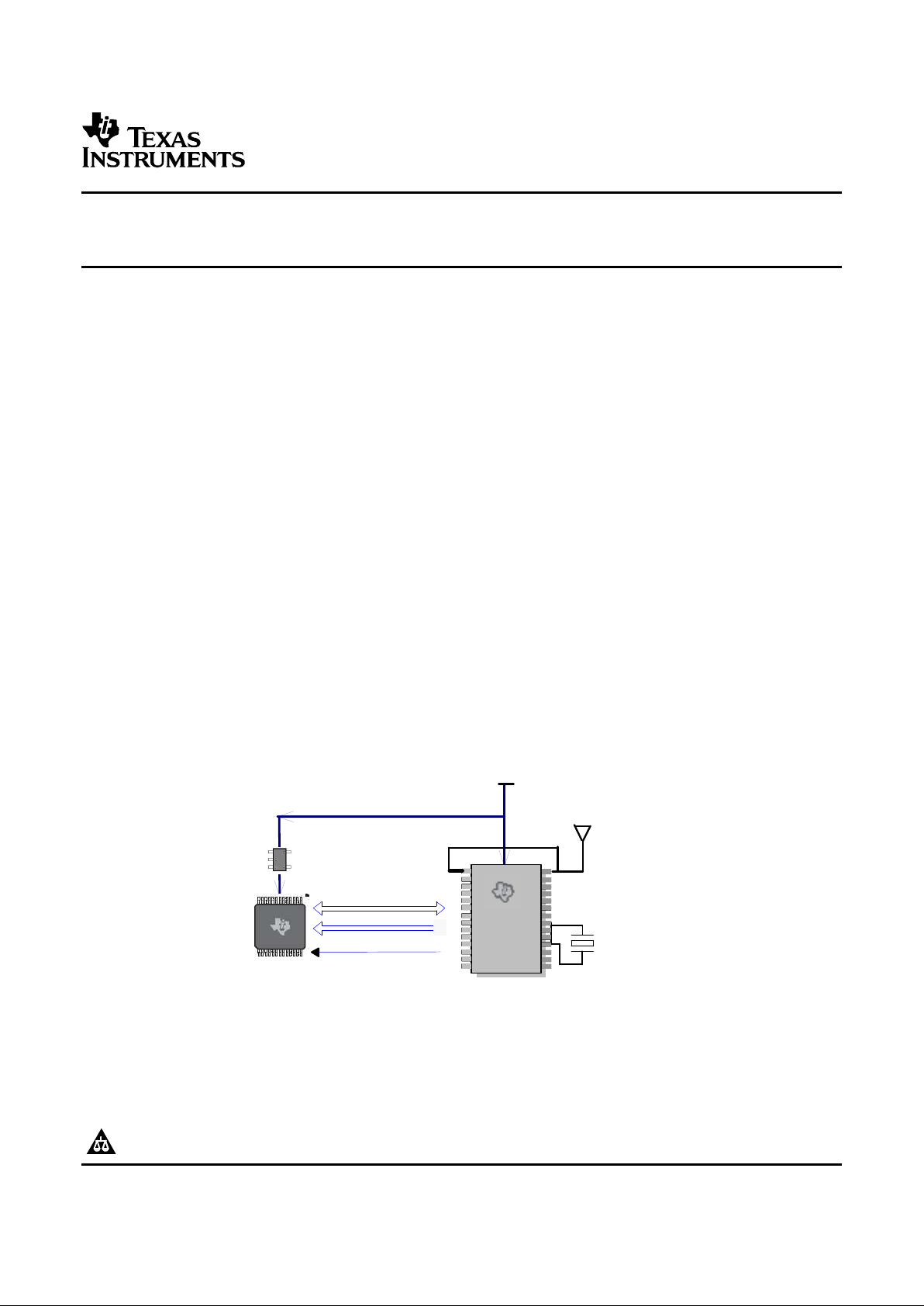
USB or PS/2
Power
I2C Control
12 MHz
Crystal
PCB Loop
Antenna
MSP430
TPS71533
2 Data Channels
6MHz for uP
TRF7900A
TRF7900A
SWRS031 – OCTOBER 2005
Fully Integrated Analog Front-End Dual Receiver Base Unit for 27-MHz Wireless Mouse
and Keyboard Systems
• High Data Throughput Rate
• 23 Discrete Components Intgrated into One – 5-kHz Square Wave Simultaneously per
Chip Channel
– Only External Components are Bypass and – 10 kbps Miller Encoded Data
Filter Capacitors, and One Crystal
• I2C Control Interface
• RF Tuner, Mixer, Transistors, Passives, Coils,
• Received Signal Strength Indicator
and Ceramic Filter Functionality All on One
• 5-V Supply
Chip
• Available in 28-Pin TSSOP (PW) Pacakge
• Integrated Phase Locked Loop
• 8 User-Selectable Frequencies
– Each Channel (Mouse and Keyboard) Can
• 27-MHz Wireless Mouse and Keyboard
Independently Select Any of the Available
Systems
Frequencies
• Human Interface Devices
• Internally Generated 6-MHz Clock to Drive
• Wireless Control
USB Microcontroller
• Remote Control Toys
• Wireless Headset
• Remote instrumentation
The TRF7900A is a dual integrated RF transceiver designed for human-interface devices (HID). Operating at 27
MHz, it integrates multiple components (PLL, RF mixer, simulated SAW filter, tuning circuit, and miscellaneous
passive components) to provide frequency selection from 8 discrete channels. This integration lowers
component, manufacturing and system costs.
The TRF7900A simplifies system design by reducing system component count and manual circuit tuning. By
integrating the PLL, SAW filter, and RF mixer, the TRF7900A eliminates the manual tuning of RLC circuits
required in traditional implementations.
Please be aware that an important notice concerning availability, standard warranty, and use in critical applications of Texas
Instruments semiconductor products and disclaimers thereto appears at the end of this data sheet.
PRODUCTION DATA information is current as of publication date.
Copyright © 2005, Texas Instruments Incorporated
Products conform to specifications per the terms of the Texas
Instruments standard warranty. Production processing does not
necessarily include testing of all parameters.

www.ti.com
ABSOLUTE MAXIMUM RATINGS
DISSIPATION RATINGS
TRF7900A
SWRS031 – OCTOBER 2005
The receiver also generates 8 frequencies that can be programmatically selected via the I2C interface bus for
both the mouse channel and/or the keyboard channel. Another 6-MHz clock is internally generated to clock the
USB microcontroller; this enables a single crystal to be used to supply the clock needs for the receiver channels
and the microcontroller.
The optimized receiver design enables simultaneous reception on both parallel channels up to 5 kHz (10 kbps
Miller encoding) per channel. A receive strength signal indicator register can be read via the I2C bus to determine
the signal strength. Correlating the RSSI reading to the packet error rate enables the controller to diagnose the
signal and understand the user condition.
ORDERING INFORMATION
PACKAGED DEVICES PACKAGE TYPE TRANSPORT MEDIA, QUANTITY
TRF7900APW TSSOP - 28 Rails, 50
TRF7900APWR TSSOP - 28 Tape and Reel, 2000
over operating free-air temperature range (unless otherwise noted)
VALUE UNIT
(1)
VS–to Supply voltage 5.5 V
V
S+
V
I
Input voltage ± VS± 0.5 V
V
ID
Differential input voltage ± 2 V
Continuous power dissipation See Dissipation Rating Table
T
J
Maximum junction temperature, any condition
(2)
150 ° C
T
J
Maximum junction temperature, continuous operation, long term 125 ° C
reliability(3)
T
stg
Storage temperature range -65 to 150 ° C
Lead temperature 1,6 mm (1/16 inch) from case for 10 seconds 300 ° C
ESD ratings: Human Body Model 4000 V
ESD ratings: Charged Device Model 1500 V
ESD ratings: Machine Model 200 V
(1) The absolute maximum ratings under any condition is limited by the constraints of the silicon process. Stresses above these ratings may
cause permanent damage. Exposure to absolute maximum conditions for extended periods may degrade device reliability. These are
stress ratings only, and functional operation of the device at these or any other conditions beyond those specified is not implied.
(2) The maximum junction temperature for continuous operation is limited by package constraints. Operation above this temperature may
result in reduced reliability and/or lifetime of the device.
POWER RATING
(2)
PACKAGE θ
JC
θ
JA
(1)
TA≤ 25 ° C TA= 85 ° C
PW (28) 13.7 56.5 1.77 W 708 mW
(1) This data was taken using the JEDEC standard high-K test PCB.
(2) Power rating is determined with a junction temperature of 125 ° C. This is the point where distortion starts to substantially increase.
Thermal management of the final PCB should strive to keep the junction temperature at or below 125 ° C for best performance and long
term reliability.
2
 Loading...