

Page 1

User's Guide
SLWU038 – August 2006
TRF2436EVM
This user’s guide provides an overview of the TRF2436 evaluation module (EVM) to
get you started using the TRF2436EVM right away. It also provides a general
description of the features and functions to be considered when using this module.
Contents
1 Introduction .......................................................................................... 1
2 TRF2436EVM Operational Procedure ........................................................... 2
3 Physical Description ................................................................................ 3
List of Figures
1 Top Layer 1 .......................................................................................... 4
2 Ground Plane Layer 2.............................................................................. 4
3 Power Plane Layer 3 ............................................................................... 5
4 Bottom Layer 4 ...................................................................................... 5
List of Tables
1 TRF2436EVM PARTS LIST ....................................................................... 6
1 Introduction
1.1 Purpose
The TRF2436 EVM provides a platform for evaluating the TRF2436 high-power, dual-band RF front-end
under various signals, reference, and supply conditions. Use this document with the EVM schematic
diagram supplied. Using the TRF2436EVM, you can rapidly evaluate the TRF2436 with a minimum of
manual setup.
1.2 System Requirements
Use the following equipment when evaluating the TRF2436EVM:
• +3.3-V power supply, 800 mA.
• Signal generator: Agilent ESG Series (with baseband I/Q modulation option for modulated testing) or
equivalent.
• Spectrum analyzer: Agilent PSA Series (with phase noise option) or equivalent.
• Vector signal analyzer: Agilent 89600 Series for 802.16x modulated EVM testing or equivalent.
1.3 Power Requirements
The demonstration board requires only one supply for proper operation. Connect +3.3 V at P1 and the
return to P2. Always terminate active PA outputs before enabling the power supply.
Voltage Limits
Exceeding the maximum input voltages can damage EVM components. Undervoltage can cause improper
operation of some or all of the EVM components.
SLWU038 – August 2006 TRF2436EVM 1
Submit Documentation Feedback
Page 2

www.ti.com
TRF2436EVM Operational Procedure
1.4 Hardware Configuration
The TRF2436EVM can be set up in a variety of configurations to accommodate a specific mode of
operation. Before starting an evaluation, decide on the configuration and make the appropriate
connections or changes. The demonstration board comes with the following factory-set configuration:
Jumper J10 installed between 1-2
Jumper J11 installed between 2-3
Jumper J12 installed between 1-2
Jumper J13 installed between 1-2
Jumper J14 installed between 1-2
LO input drive
The TRF2436 has been designed to be driven with a differential LO input. A simple balun centered at ~2.6
GHz can be used to convert a single-ended input from an RF source to a differential pair to provide a
differential LO to the EVM through SMA connectors J3 and J4.
The 2436 will function if driven single-ended, but it is not designed to operate in this condition, nor has it
been evaluated in this condition. To drive the LO single-ended, connect an RF source to the LOP SMA
(J3) and terminate the LON SMA (J4) input with 50 Ω .
Filtering
The TRF2436EVM is provided with no filtering. The mixer output, PA input/LNA output, and RF
input/output pins are brought out directly to SMA connectors on the EVM. Filtering may be incorporated
by:
• Connecting an external filter to RFANTA (J6) for filtering after the PA in TX mode or before the LNA in
RX mode.
• Connecting an external filter between the MFA (J8) and RFA (J9) jacks for filtering between the mixer
and PA/LNA stages
2 TRF2436EVM Operational Procedure
2.1 TX Operation
1. Connect +3.3 V to P1 and ground to P2 but do not turn on.
2. Connect differential LO source to LOP/LON jacks (or use external balun).
Set the appropriate frequency and power level between 0 to +4 dBm. Remember that for A-band
operation, the LO input frequency is doubled inside the TRF2436; so, the LO should be set to half the
frequency desired at the mixer LO port.
3. Connect an IF source to the IF port. Set to 374 MHz with a typical power level of –20 dBm.
4. Set ABSEL (J12) to a logic high 1.
5. Set TR (J13) to a logic high 1.
6. Set PA_B SEL (J11) to a logic low 0.
7. Set PA_A SEL (J10) to logic high 1.
8. RXDGC = don’t care
9. For mixer stage measurement:
a. Terminate RFA (J9) and RFANTA (J6) into 50 Ω .
b. Connect a spectrum analyzer to MFA (J8).
c. Turn on the 3.3-V power supply (~300 mA to 320 mA).
d. Observe the output of the mixer stage on a spectrum analyzer.
10. For PA stage measurement:
a. Terminate IF (J7) and MFA (J8) into 50 Ω .
b. Apply an RF to RFA (J9).
c. Connect a spectrum analyzer to RFANTA (J6).
d. Turn on the power supply.
e. Observe the PA output on a spectrum analyzer.
TRF2436EVM 2 SLWU038 – August 2006
Submit Documentation Feedback
Page 3

www.ti.com
Physical Description
2.2 RX Operation
1. Set TR (J13) to logic 0.
2. Set PA_A SEL (J10) to logic 0.
3. Connect a differential LO source to the LOP/LON SMAs (or use an external balun).
Set the LO to an appropriate frequency, with the power level between 0 to +4 dBm. Remember that for
A-band operation, the LO input frequency is doubled inside the TRF2436; so, the LO should be set to
half the frequency desired at the mixer LO port.
4. For mixer stage measurement:
a. Terminate RFA (J9) and RFANTA (J6) into 50 Ω .
b. Connect an RF source to MFA (J8). Set to a desired RF frequency and typical power level
of –20 dBm.
c. Connect a spectrum analyzer to the IF (J7) output.
d. Turn on the 3.3-V power supply (~90 mA).
e. Observe the IF output on a spectrum analyzer (374 MHz).
5. For LNA stage measurement:
a. Terminate IF (J7) and MFA (J8) into 50 Ω .
b. Connect an RF source to RFANTA (J6). Set to a desired frequency and typical power
level of –40 dBm.
c. Connect a spectrum analyzer to RFA (J9).
d. Turn on the power supply.
e. Observe the LNA output on a spectrum analyzer.
f. Use jumper J14 (RXDGC) to select between LNA high (pins 2-3) and low gain (pins 1-2)
modes.
3 Physical Description
This section describes the physical characteristics and PCB layout of the EVM and lists the components
used on the module.
SLWU038 – August 2006 TRF2436EVM 3
Submit Documentation Feedback
Page 4
www.ti.com
Physical Description
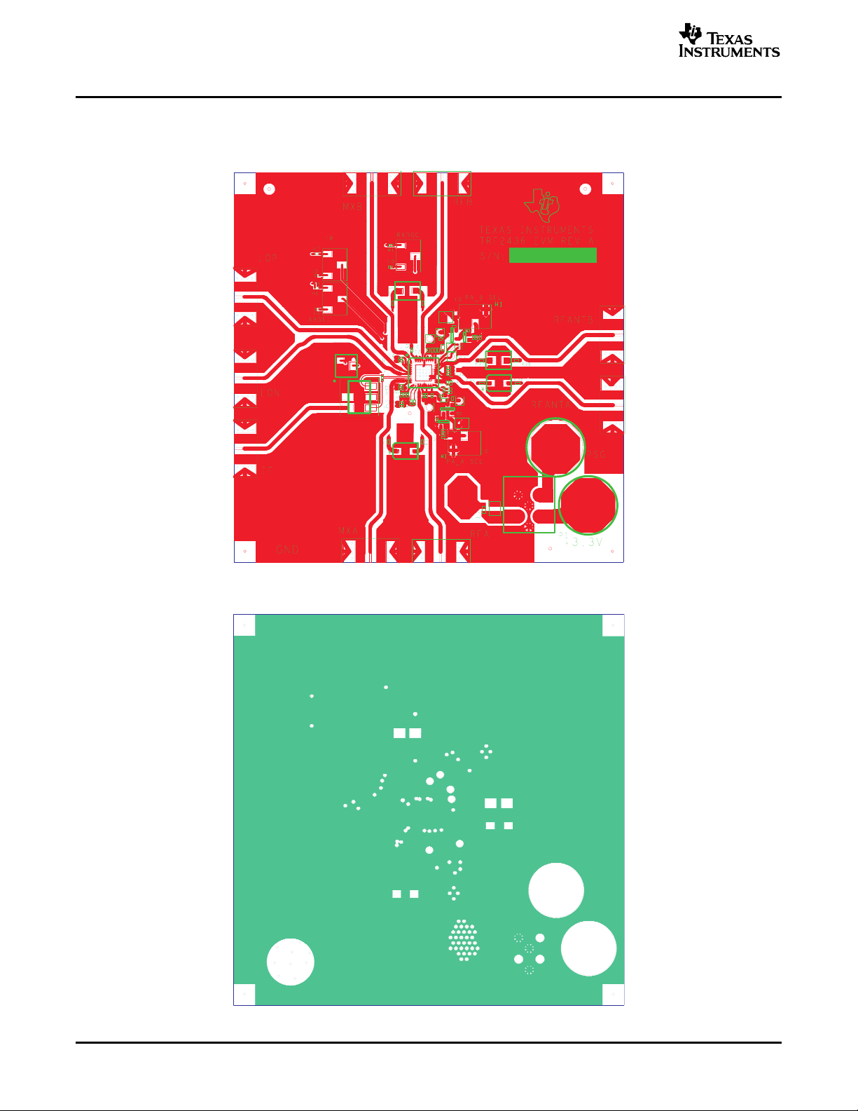
3.1 PCB Layout
The EVM is constructed on a 4-layer, 3.6-inch × 3.6-inch, 0.042-inch thick PCB using Polycad 370
Turbo/HR material. Figure 1 through Figure 4 show the PCB layout for the EVM.
Figure 1. Top Layer 1
Figure 2. Ground Plane Layer 2
4 TRF2436EVM SLWU038 – August 2006
Submit Documentation Feedback
Page 5

www.ti.com
Physical Description
Figure 3. Power Plane Layer 3
Figure 4. Bottom Layer 4
SLWU038 – August 2006 TRF2436EVM 5
Submit Documentation Feedback
Page 6

www.ti.com
Physical Description
3.2 Part List
Table 1 lists the parts used in constructing the EVM.
Table 1. TRF2436EVM PARTS LIST
QTY Ref Value Part Number Note
1 C1 470pF GRM033R71C471KD
1 C2 10pF GRM1555C1H100JZ
1 C3 5600pF C0402C562K3RACT
7 C4 C6 C11 C15 C17 C24 0.01 µ F GRM155R71E103KA
C33
12 C5 C9 C12–C14 C16 C19 100pF GRM1555C1H101JD
C20 C22 C25 C26 C31
3 C7 C8 C18 10 µ F ECJ-4YB1A106K
3 C10 C23 C29 1000pF GRM155R71H102KA
2 C21 C32 1.2pF 04025A1R2BAT2A
1 C28 0.1 µ F ECJ-0EB1A104K
2 FL1 FL2 Filter, 2400–2484MHz DFCB22G44LBJAA DNI
2 FL3 FL4 Filter, 5597.5MHz DFCB35G59LAHAA DNI
1 FL5 Filter Block, DC power BNX002-01
9 J1–J9 MXB SMA 142-0701-841
5 J10–J14 PA_A SEL 54201-S08-3
4 L1 R3 R4 R31 DNI
3 L2 L3 L7 27 Ω at 100MHz EXC-ML16A270U
4 L6 L8 L10 L12 120 Ω at 100MHz BLM15AG102SN1D
2 L9 L11 33nH LQW15AN33NJ00D
1 P1 +3.3V_IN ST-351A
1 P2 PSG ST-351B
2 Q1 Q3 IRLML6401 IRLML6401
2 Q2 Q4 MMST2222A MMST2222A-7
8 R1 R2 R6 R7 R35–R38 TRACE GAP, NO PART DNI
1 R5 634 ERJ-2RKF6340X
9 R8–R13 R15 R32 R33 10K ERJ-2GEJ103X
7 R16–R18 R24 R25 R28 1K ERJ-2GEJ102X
R29
4 R20–R23 200 ERJ-2RKF2000X
1 R26 750 ERJ-2GEJ751X
1 R27 2K POT 3214W-1-202E
1 R30 5.1K ERJ-2GEJ512X
1 T1 ADT4-1T ADT4-1T
6 TP1–TP6 T POINT R 5015
1 U1 TRF2436 TRF2436
2 U2 U3 MMDT3906 MMDT3906-7
1 U4 MMDT3904 MMDT3904-7
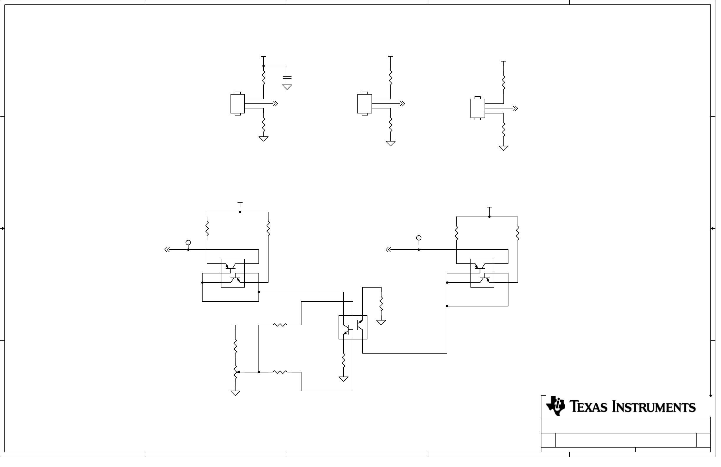
3.3 Schemtic Drawing
The schematic drawing for the TRF2436EVM appears on the following page.
6 TRF2436EVM SLWU038 – August 2006
Submit Documentation Feedback
Page 7

5
4
MXB SMA
MXB SMA
3
J1
J1
1 2
3
RFB SMA
RFB SMA
3
J2
J2
1 2
2
1
D D
LOP SMA
LOP SMA
MXB_SMA
TRACE GAP, NO PART
TRACE GAP, NO PART
R1
R1
J3
J3
3
12
50 OHM
MXB
12
DFCB22G44LBJAA_DNI
DFCB22G44LBJAA_DNI
FL1
FL1
IN1OUT
Filter, 2400-2484 MHz
Filter, 2400-2484 MHz
DNI
DNI
TRACE GAP, NO PART
TRACE GAP, NO PART
R2
RFB
2
R2
50 OHM
L1
DNIL1DNI
1 2
C14
C14
100pF
100pF
VDD
50 OHM
LOADJB
TR
1 2
ABSEL
LOADJA
LOP
LON
IFP
IFN
10
1
2
3
4
5
6
7
8
9
U1
U1
MXB
ABSEL
V+LOB
LOADJA
LOP
LON
IFP
IFN
MXA
L+LOA
39
41
40
38
TR
BACK
LOADJB
TXGADJB
TRF 2436
TRF 2436
V+IF11V+IFP12V+IFN13RFA14V+PA1A15V+GEN16V+PA2A17PABCA18V+PA3A19BCOUT
V+IFN
V+IFP
V+IF
J4
J4
3
12
C C
LON SMA
LON SMA
3
IF SMA
IF SMA
B B
J7
J7
12
50 OHM
IF_SMA
50 OHM
ADT4-1T
ADT4-1T
1 6
2
3 4
T1
T1
5
VDD
100 OHM
100 OHM
C15
C15
.01uF
.01uF
1 2
C16
C16
100pF
100pF
RXDGC
37
RXDGC
34
35
36
RFB
RSVD1
V+PA1A
V+GEN
V+PA1B
PABCB
32
33
PABCB
V+PA1B
PABCA
V+PA2A
12
BCIN
V+PA2B
31
V+PA3B
BCIN
V+PA2B
RFANTB
V+LNABA
RFANTA
BYPOUT
20
BCOUT
V+PA3A
RFB_SMA
DETP
DETN
GND2
GND1
BYPIN
30
29
28
27
26
25
24
23
22
21
R5
1 2
634R5634
12
C3
C3
5600 pF
5600 pF
V+PA3B
DETP
DETN
V+LNABA
TP1TP1
12
12
1
TP2TP2
RFANTB
RFANTA
BYPOUT
C1
C1
470pF
470pF
C4
C4
0.01uF
0.01uF
1 2
1
R3
1 2
DNIR3DNI
R4
DNIR4DNI
50 OHM
50 OHM
12
BCIN
TRACE GAP, NO PART
TRACE GAP, NO PART
TRACE GAP, NO PART
TRACE GAP, NO PART
C2
10pFC210pF
R37
R37
R35
R35
FL2
12
12
FL2
IN1OUT
Filter, 2400-2484 MHz
Filter, 2400-2484 MHz
DFCB22G44LBJAA_DNI
DFCB22G44LBJAA_DNI
DNI
DNI
IN1OUT
Filter, 5597.5MHz
Filter, 5597.5MHz
DFCB35G59LAHAA_DNI
DFCB35G59LAHAA_DNI
FL3
FL3
DNI
DNI
TRACE GAP, NO PART
TRACE GAP, NO PART
FANTB_SFANTB
2
TRACE GAP, NO PART
TRACE GAP, NO PART
FANTA_SFANTA
2
R38
R38
R36
R36
12
12
J5
J5
3
1 2
J6
J6
3
1 2
RFANTB SMA
RFANTB SMA
RFANTA SMA
RFANTA SMA
50 OHM
TRACE GAP, NO PART
TRACE GAP, NO PART
TRACE GAP, NO PART
R6
R6
1 2
A A
5
4
MXA_SMA
3
12
J8
J8
MXA SMA
MXA SMA
MXA RFA
Filter, 5597.5MHz
Filter, 5597.5MHz
DFCB35G59LAHAA_DNI
DFCB35G59LAHAA_DNI
TRACE GAP, NO PART
FL4
FL4
IN1OUT
DNI
DNI
2
50 OHM
R7
R7
1 2
3
3
RFA_SMA
12
J9
J9
RFA SMA
RFA SMA
Engineer:
Drawn By:
M. ARNOLD
L. NGUYEN
2
Title
Title
Title
TRF2436 Evaluation Module
TRF2436 Evaluation Module
TRF2436 Evaluation Module
Size Document Number Rev
Size Document Number Rev
Size Document Number Rev
B
B
B
Date: Sheet of
Date: Sheet of
Date: Sheet
TRF2436EVM-SCH
TRF2436EVM-SCH
TRF2436EVM-SCH
13Monday, April 17, 2006
13Monday, April 17, 2006
1
13Monday, April 17, 2006
of
A
A
A
Page 8

5
P1
P1
FL5
RED
RED
BLK
BLK
3.3V_IN
1
PSG
1
+3.3V_IN
+3.3V_IN
D D
PSG
PSG
P2
P2
1
1
FL5
B
PSG
Filter Block, DC power
Filter Block, DC power
Murata BNX002-01
Murata BNX002-01
CG3
CB
CG2
CG1
GND
GND
C8
10uFC810uF
4
L2
L2
1 2
27 OHM @ 100MHz
27 OHM @ 100MHz
VDD
V+PA1A
V+PA2A
V+PA3A
12
12
12
C5
C5
100pF
100pF
C9
C9
100pF
100pF
C13
C13
100pF
100pF
3
12
27 OHM @ 100MHz
27 OHM @ 100MHz
12
C10
C10
1000pF
1000pF
12
C6
.01uFC6.01uF
TP3TP3
L3
L3
3
12
C11
C11
.01uF
.01uF
IRLML6401
IRLML6401
C7
10uFC710uF
Q1
Q1
2
VDD
VDD
2
1
R8
10KR810K
3
Q2
Q2
1
MMST2222A
MMST2222A
2
R9
10KR910K
C12
C12
1 2
100pF
100pF
VDD
1
2
3
PA_A SEL
R32
R32
10K
10K
PA_A SEL
12
J10
J10
1
C C
C18
C18
10uF
10uF
VDD
VDD
R10
2
1
R10
10K
10K
3
Q4
Q4
1
MMST2222A
MMST2222A
2
R11
R11
10K
10K
C25
C25
1 2
100pF
100pF
VDD
1
J11
J11
2
3
PA_B SEL
PA_B SEL
12
R33
R33
10K
10K
VDD
VDD
B B
VDD
120 ohm @100MHz
120 ohm @100MHz
L6
L6
120 ohm @100MHz
120 ohm @100MHz
L8
L8
C20
C20
100pF
100pF
1 2
L9
33nHL933nH
C21
C21
1.2pF
1.2pF
V+IF
1 2
5 MIL trace
VDD
120 ohm @ 100MHz
120 ohm @ 100MHz
V+IFP
L10
L10
120 ohm @ 100MHz
120 ohm @ 100MHz
L12
L12
C31
C31
100pF
100pF
C28
C28
.1uF
.1uF
1 2
1 2
C32
C32
1.2pF
1.2pF
V+GEN
V+LNABA
1 2
V+PA1B
V+PA2B
V+PA3B
12
12
12
C19
C19
100pF
100pF
C22
C22
100pF
100pF
C26
C26
100pF
100pF
L7
L7
27 OHM @ 100MHz
27 OHM @ 100MHz
12
C23
C23
1000pF
1000pF
TP4TP4
12
C17
C17
.01uF
.01uF
3
12
C24
C24
.01uF
.01uF
12
Q3
Q3
IRLML6401
IRLML6401
L11
C29
C29
12
1000pF
1000pF
A A
5
L11
33nH
33nH
5 MIL trace
V+IFN
LOADJB
R31
R31
DNI
DNI
4
R30
R30
5.1K
5.1K
3
LOADJA
Title
Title
Title
TRF2436 Evaluation Module
TRF2436 Evaluation Module
TRF2436 Evaluation Module
Size Document Number Rev
Size Document Number Rev
Size Document Number Rev
B
B
B
Date: Sheet of
Date: Sheet of
2
Date: Sheet
TRF2436EVM-SCH
TRF2436EVM-SCH
TRF2436EVM-SCH
23Thursday, April 13, 2006
23Thursday, April 13, 2006
1
23Thursday, April 13, 2006
of
A
A
A
Page 9
5
4
3
2
1
VDD VDD
D D
12
.01uF
ABSEL
.01uF
C33
C33
J13TRJ13
TR
R13
R13
10K
10K
1
2
3
R171KR17
1K
TR
TP6TP6
R22
R22
200
200
J14
J14
RXDGC
RXDGC
R12
R12
10K
10K
1
J12
J12
2
3
ABSEL
ABSEL
C C
VDD
R20
R20
200
200
TP5TP5
R161KR16
1K
R21
R21
200
200
1
2
3
VDD
VDD
R15
R15
10K
10K
R181KR18
1K
RXDGC
R23
R23
200
200
PABCA PABCB
B B
A A
E1
B1
C2
2K POT
2K POT
U2
U2
MMDT3906
MMDT3906
VDD
R26
R26
750
750
R27
R27
C1
B2
E2
R251KR25
1K
R291KR29
1K
U4
U4
MMDT3904
MMDT3904
R281KR28
1K
C1
E1
B2
B1
E2
C2
R241KR24
1K
E1
B1
C2
U3
U3
MMDT3906
MMDT3906
C1
B2
E2
Title
Title
Title
TRF2436 Evaluation Module
TRF2436 Evaluation Module
TRF2436 Evaluation Module
Size Document Number Rev
Size Document Number Rev
Size Document Number Rev
B
B
B
Date: Sheet
Date: Sheet of
5
4
3
2
Date: Sheet of
TRF2436EVM-SCH
TRF2436EVM-SCH
TRF2436EVM-SCH
33Thursday, April 13, 2006
33Thursday, April 13, 2006
1
33Thursday, April 13, 2006
of
A
A
A
Page 10

EVALUATION BOARD/KIT IMPORTANT NOTICE
Texas Instruments (TI) provides the enclosed product(s) under the following conditions:
This evaluation board/kit is intended for use for ENGINEERING DEVELOPMENT, DEMONSTRATION, OR EVALUATION
PURPOSES ONLY and is not considered by TI to be a finished end-product fit for general consumer use. Persons handling the
product(s) must have electronics training and observe good engineering practice standards. As such, the goods being provided are
not intended to be complete in terms of required design-, marketing-, and/or manufacturing-related protective considerations,
including product safety and environmental measures typically found in end products that incorporate such semiconductor
components or circuit boards. This evaluation board/kit does not fall within the scope of the European Union directives regarding
electromagnetic compatibility, restricted substances (RoHS), recycling (WEEE), FCC, CE or UL, and therefore may not meet the
technical requirements of these directives or other related directives.
Should this evaluation board/kit not meet the specifications indicated in the User’s Guide, the board/kit may be returned within 30
days from the date of delivery for a full refund. THE FOREGOING WARRANTY IS THE EXCLUSIVE WARRANTY MADE BY
SELLER TO BUYER AND IS IN LIEU OF ALL OTHER WARRANTIES, EXPRESSED, IMPLIED, OR STATUTORY, INCLUDING
ANY WARRANTY OF MERCHANTABILITY OR FITNESS FOR ANY PARTICULAR PURPOSE.
The user assumes all responsibility and liability for proper and safe handling of the goods. Further, the user indemnifies TI from all
claims arising from the handling or use of the goods. Due to the open construction of the product, it is the user’s responsibility to
take any and all appropriate precautions with regard to electrostatic discharge.
EXCEPT TO THE EXTENT OF THE INDEMNITY SET FORTH ABOVE, NEITHER PARTY SHALL BE LIABLE TO THE OTHER
FOR ANY INDIRECT, SPECIAL, INCIDENTAL, OR CONSEQUENTIAL DAMAGES.
TI currently deals with a variety of customers for products, and therefore our arrangement with the user is not exclusive.
TI assumes no liability for applications assistance, customer product design, software performance, or infringement of
patents or services described herein.
Please read the User’s Guide and, specifically, the Warnings and Restrictions notice in the User’s Guide prior to handling the
product. This notice contains important safety information about temperatures and voltages. For additional information on TI’s
environmental and/or safety programs, please contact the TI application engineer or visit www.ti.com/esh .
No license is granted under any patent right or other intellectual property right of TI covering or relating to any machine, process, or
combination in which such TI products or services might be or are used.
FCC Warning
This evaluation board/kit is intended for use for ENGINEERING DEVELOPMENT, DEMONSTRATION, OR EVALUATION
PURPOSES ONLY and is not considered by TI to be a finished end-product fit for general consumer use. It generates, uses, and
can radiate radio frequency energy and has not been tested for compliance with the limits of computing devices pursuant to part 15
of FCC rules, which are designed to provide reasonable protection against radio frequency interference. Operation of this
equipment in other environments may cause interference with radio communications, in which case the user at his own expense
will be required to take whatever measures may be required to correct this interference.
EVM WARNINGS AND RESTRICTIONS
It is important to operate this EVM within the input voltage range of 0 V to 3.3 V and the output voltage range of 0 V to 3.3 V.
Exceeding the specified input range may cause unexpected operation and/or irreversible damage to the EVM. If there are
questions concerning the input range, please contact a TI field representative prior to connecting the input power.
Applying loads outside of the specified output range may result in unintended operation and/or possible permanent damage to the
EVM. Please consult the EVM User's Guide prior to connecting any load to the EVM output. If there is uncertainty as to the load
specification, please contact a TI field representative.
During normal operation, some circuit components may have case temperatures greater than 85 ° C. The EVM is designed to
operate properly with certain components above 85 ° C as long as the input and output ranges are maintained. These components
include but are not limited to linear regulators, switching transistors, pass transistors, and current sense resistors. These types of
devices can be identified using the EVM schematic located in the EVM User's Guide. When placing measurement probes near
these devices during operation, please be aware that these devices may be very warm to the touch.
Mailing Address: Texas Instruments, Post Office Box 655303, Dallas, Texas 75265
Copyright © 2006, Texas Instruments Incorporated
Page 11

IMPORTANT NOTICE
Texas Instruments Incorporated and its subsidiaries (TI) reserve the right to make corrections, modifications, enhancements,
improvements, and other changes to its products and services at any time and to discontinue any product or service without notice.
Customers should obtain the latest relevant information before placing orders and should verify that such information is current and
complete. All products are sold subject to TI’s terms and conditions of sale supplied at the time of order acknowledgment.
TI warrants performance of its hardware products to the specifications applicable at the time of sale in accordance with TI’s
standard warranty. Testing and other quality control techniques are used to the extent TI deems necessary to support this
warranty. Except where mandated by government requirements, testing of all parameters of each product is not necessarily
performed.
TI assumes no liability for applications assistance or customer product design. Customers are responsible for their products and
applications using TI components. To minimize the risks associated with customer products and applications, customers should
provide adequate design and operating safeguards.
TI does not warrant or represent that any license, either express or implied, is granted under any TI patent right, copyright, mask
work right, or other TI intellectual property right relating to any combination, machine, or process in which TI products or services
are used. Information published by TI regarding third-party products or services does not constitute a license from TI to use such
products or services or a warranty or endorsement thereof. Use of such information may require a license from a third party under
the patents or other intellectual property of the third party, or a license from TI under the patents or other intellectual property of TI.
Reproduction of information in TI data books or data sheets is permissible only if reproduction is without alteration and is
accompanied by all associated warranties, conditions, limitations, and notices. Reproduction of this information with alteration is an
unfair and deceptive business practice. TI is not responsible or liable for such altered documentation.
Resale of TI products or services with statements different from or beyond the parameters stated by TI for that product or service
voids all express and any implied warranties for the associated TI product or service and is an unfair and deceptive business
practice. TI is not responsible or liable for any such statements.
TI products are not authorized for use in safety-critical applications (such as life support) where a failure of the TI product would
reasonably be expected to cause severe personal injury or death, unless officers of the parties have executed an agreement
specifically governing such use. Buyers represent that they have all necessary expertise in the safety and regulatory ramifications
of their applications, and acknowledge and agree that they are solely responsible for all legal, regulatory and safety-related
requirements concerning their products and any use of TI products in such safety-critical applications, notwithstanding any
applications-related information or support that may be provided by TI. Further, Buyers must fully indemnify TI and its
representatives against any damages arising out of the use of TI products in such safety-critical applications.
TI products are neither designed nor intended for use in military/aerospace applications or environments unless the TI products are
specifically designated by TI as military-grade or "enhanced plastic." Only products designated by TI as military-grade meet military
specifications. Buyers acknowledge and agree that any such use of TI products which TI has not designated as military-grade is
solely at the Buyer's risk, and that they are solely responsible for compliance with all legal and regulatory requirements in
connection with such use.
TI products are neither designed nor intended for use in automotive applications or environments unless the specific TI products
are designated by TI as compliant with ISO/TS 16949 requirements. Buyers acknowledge and agree that, if they use any
non-designated products in automotive applications, TI will not be responsible for any failure to meet such requirements.
Following are URLs where you can obtain information on other Texas Instruments products and application solutions:
Products Applications
Amplifiers amplifier.ti.com Audio www.ti.com/audio
Data Converters dataconverter.ti.com Automotive www.ti.com/automotive
DSP dsp.ti.com Broadband www.ti.com/broadband
Interface interface.ti.com Digital Control www.ti.com/digitalcontrol
Logic logic.ti.com Military www.ti.com/military
Power Mgmt power.ti.com Optical Networking www.ti.com/opticalnetwork
Microcontrollers microcontroller.ti.com Security www.ti.com/security
RFID www.ti-rfid.com Telephony www.ti.com/telephony
Low Power www.ti.com/lpw Video & Imaging www.ti.com/video
Wireless
Wireless www.ti.com/wireless
Mailing Address: Texas Instruments, Post Office Box 655303, Dallas, Texas 75265
Copyright © 2007, Texas Instruments Incorporated
 Loading...