

www.ti.com
1
2
3
4
5
6
GND
DCQ PACKAGE
SOT223-6
(TOP VIEW)
NR/FB
OUT
GND
IN
EN
1
KTT (DDPAK) PACKAGE
(TOP VIEW)
2
3
4
5
EN
IN
GND
OUT
NR/FB
0.0
0.1
0.2
0.3
0.4
0.5
0.6
0.7
Frequency (Hz)
100 10k 100k1k
Output Spectral Noise Density − µV/√Hz
I
OUT
= 1 mA
TPS79630
OUTPUT SPECTRAL NOISE DENSITY
vs
FREQUENCY
I
OUT
= 1.5 A
VIN = 5.5 V
C
OUT
= 2.2 µF
CNR = 0.1 µF
0
10
20
30
40
50
60
70
80
Frequency (Hz)
1 10k 10M1k
Ripple Rejection − dB
I
OUT
= 1 mA
TPS79630
RIPPLE REJECTION
vs
FREQUENCY
I
OUT
= 1 A
VIN = 4 V
C
OUT
= 10 µF
CNR = 0.01 µF
10 100 100k 1M
EN
NC
GND
NR
8
7
6
5
IN
IN
OUT
OUT
1
2
3
4
DRB PACKAGE
3mm x 3mm SON
(TOP VIEW)
ULTRALOW-NOISE, HIGH PSRR, FAST, RF, 1A
LOW-DROPOUT LINEAR REGULATORS
FEATURES DESCRIPTION
• 1A Low-Dropout Regulator With Enable
• Available in Fixed and Adjustable (1.2V to
5.5V) Versions
• High PSRR (53dB at 10kHz)
• Ultralow-Noise (40 µ V
• Fast Start-Up Time (50 µ s)
• Stable With a 1 µ F Ceramic Capacitor
• Excellent Load/Line Transient Response
• Very Low Dropout Voltage (250mV at Full
Load, TPS79630)
• 3 × 3 SON, SOT223-6, and
DDPAK-5 Packages
APPLICATIONS
• RF: VCOs, Receivers, ADCs
• Audio
• Bluetooth™, Wireless LAN
• Cellular and Cordless Telephones
• Handheld Organizers, PDAs
, TPS79630)
RMS
TPS796xx
SLVS351I – SEPTEMBER 2002 – REVISED MAY 2006
The TPS796xx family of low-dropout (LDO)
low-power linear voltage regulators features high
power supply rejection ratio (PSRR), ultralow-noise,
fast start-up, and excellent line and load transient
responses in small outline, 3 × 3 SON, SOT223-6,
and DDPAK-5 packages. Each device in the family is
stable with a small 1 µ F ceramic capacitor on the
output. The family uses an advanced, proprietary
BiCMOS fabrication process to yield extremely low
dropout voltages (e.g., 250mV at 1A). Each device
achieves fast start-up times (approximately 50 µ s with
a 0.001 µ F bypass capacitor) while consuming very
low quiescent current (265 µ A typical). Moreover,
when the device is placed in standby mode, the
supply current is reduced to less than 1 µ A. The
TPS79630 exhibits approximately 40 µ V
voltage noise at 3.0V output, with a 0.1 µ F bypass
capacitor. Applications with analog components that
are noise sensitive, such as portable RF electronics,
benefit from the high PSRR, low noise features, and
the fast response time.
of output
RMS
Please be aware that an important notice concerning availability, standard warranty, and use in critical applications of Texas
Instruments semiconductor products and disclaimers thereto appears at the end of this data sheet.
Bluetooth is a trademark of Bluetooth SIG, Inc.
All other trademarks are the property of their respective owners.
PRODUCTION DATA information is current as of publication date.
Products conform to specifications per the terms of the Texas
Instruments standard warranty. Production processing does not
necessarily include testing of all parameters.
Copyright © 2002–2006, Texas Instruments Incorporated
www.ti.com
TPS796xx
SLVS351I – SEPTEMBER 2002 – REVISED MAY 2006
This integrated circuit can be damaged by ESD. Texas Instruments recommends that all integrated circuits be handled with
appropriate precautions. Failure to observe proper handling and installation procedures can cause damage.
ESD damage can range from subtle performance degradation to complete device failure. Precision integrated circuits may be
more susceptible to damage because very small parametric changes could cause the device not to meet its published
specifications.
ORDERING INFORMATION
PRODUCT V
(1)
(2)
OUT
TPS796 xxyyyz XX is nominal output voltage (for example, 28 = 2.8V, 01 = Adjustable).
YYY is package designator.
Z is package quantity.
(1) For the most current package and ordering information, see the Package Option Addendum at the end of this document, or see the TI
web site at www.ti.com .
(2) Output voltages from 1.3V to 4.9V in 100mV increments are available; minimum order quantities may apply. Contact factory for details
and availability.
ABSOLUTE MAXIMUM RATINGS
over operating temperature range (unless otherwise noted)
VINrange –0.3V to 6V
V
range –0.3V to VIN+ 0.3V
EN
V
range 6V
OUT
Peak output current Internally limited
ESD rating, HBM 2kV
ESD rating, CDM 500V
Continuous total power dissipation See Dissipation Ratings Table
Junction temperature range, T
Storage temperature range, T
(1) Stresses beyond those listed under absolute maximum ratings may cause permanent damage to the device. These are stress ratings
only, and functional operation of the device at these or any other conditions beyond those indicated under recommended operating
conditions is not implied. Exposure to absolute-maximum-rated conditions for extended periods may affect device reliability.
J
stg
(1)
UNIT
–40 ° C to +150 ° C
–65 ° C to +150 ° C
PACKAGE DISSIPATION RATINGS
PACKAGE BOARD R
DDPAK High-K
SOT223 Low-K
3 × 3 SON High-K
(1)
(2)
(1)
(1) The JEDEC high-K (2s2p) board design used to derive this data was a 3-inch × 3-inch (7,5-cm × 7,5-cm), multilayer board with 1-ounce
internal power and ground planes and 2-ounce copper traces on top and bottom of the board.
(2) The JEDEC low-K (1s) board design used to derive this data was a 3-inch × 3-inch (7,5-cm × 7,5-cm), two-layer board with 2-ounce
copper traces on top of the board.
2
Submit Documentation Feedback
θ JC
2 ° C/W 23 ° C/W
15 ° C/W 53 ° C/W
1.2 ° C/W 40 ° C/W
R
θ JA
www.ti.com
TPS796xx
SLVS351I – SEPTEMBER 2002 – REVISED MAY 2006
ELECTRICAL CHARACTERISTICS
over recommended operating temperature range (T
C
= 10 µ F, and C
OUT
= 0.01 µ F, unless otherwise noted. Typical values are at +25 ° C.
NR
= –40 ° C to +125 ° C), V
J
= V
, V
EN
= V
IN,
IN
OUT(nom)
PARAMETER TEST CONDITIONS MIN TYP MAX UNIT
VINInput voltage
V
Internal reference (TPS79601) 1.200 1.225 1.250 V
FB
I
Continuous output current 0 1 A
OUT
(1)
2.7 5.5 V
Output
voltage TPS79601 1.225 5.5 – V
range
Output
voltage
Accuracy V
TPS79601
Fixed
OUT
Fixed
V
OUT
Output voltage line regulation
( ∆ V
OUT
Load regulation ( ∆ V
(1)
%/V
)
IN
%/ ∆ I
OUT
OUT
TPS79628 I
Dropout voltage
(V
= V
IN
(3)
OUT (nom)
– 0.1V)
TPS79628DRB I
TPS79630 I
TPS79633 I
TPS79650 I
Output current limit V
Ground pin current 0 µ A ≤ I
Shutdown current
(4)
FB pin current V
Power-supply ripple
rejection
TPS79630 dB
Output noise voltage (TPS79630) µ V
Time, start-up (TPS79630) RL= 3 Ω , C
EN pin current V
(2)
0 µ A ≤ I
< 5V
= 5V
0 µ A ≤ I
0 µ A ≤ I
V
OUT
) 0 µ A ≤ I
OUT
OUT
OUT
OUT
OUT
OUT
V
EN
FB
f = 100Hz, I
f = 100Hz, I
f = 10Hz, I
f = 100Hz, I
BW = 100Hz to 100kHz,
I
OUT
EN
≤ 1A, V
OUT
≤ 1A, V
OUT
≤ 1A, V
OUT
OUT
OUT
OUT
+ 1V ≤ VIN≤ 5.5V
+ 1V ≤ VIN≤ 5.5V
+ 1V ≤ VIN≤ 5.5V
+ 1V ≤ VIN≤ 5.5V 0.05 0.12 %/V
≤ 1A 5 mV
OUT
= 1A 270 365
= 250mA 52 90
= 1A 250 345 mV
= 1A 220 325
= 1A 200 300
= 0V 2.4 4.2 A
≤ 1A 265 385 µ A
OUT
= 0V, 2.7V ≤ VIN≤ 5.5V 0.07 1 µ A
= 1.225V 1 µ A
= 10mA 59
OUT
= 1A 54
OUT
= 1A 53
OUT
= 1A 42
OUT
C
NR
C
= 1A
= 1 µ F C
OUT
NR
C
NR
C
NR
C
NR
NR
C
NR
= 0V –1 1 µ A
(1)
(1)
(1)
0.98V
OUT
–2.0 +2.0 %
–3.0 +3.0 %
= 0.001 µ F 54
= 0.0047 µ F 46
= 0.01 µ F 41
= 0.1 µ F 40
= 0.001 µ F 50
= 0.0047 µ F 75 µ s
= 0.01 µ F 110
High-level enable input voltage 2.7V ≤ VIN≤ 5.5V 1.7 V
Low-level enable input voltage 2.7V ≤ VIN≤ 5.5V 0 0.7 V
+ 1 V
V
(1)
, I
= 1mA,
OUT
DD
1.02V
OUT
OUT
IN
V
V
RMS
V
(1) Minimum VIN= V
(2) Tolerance of external resistors not included in this specification.
(3) V
(4) For adjustable version, this applies only after VINis applied; then V
is not measured for TPS79618 and TPS79625 because minimum VIN= 2.7V.
DO
+ V
OUT
or 2.7V, whichever is greater. TPS79650 is tested at VIN= 5.5V.
DO
Submit Documentation Feedback
transitions high to low.
EN
3
www.ti.com
_
+
Thermal
Shutdown
Bandgap
Reference
1.225 V
V
IN
Current
Sense
R
2
GND
EN
SHUTDOWN
V
REF
UVLO
ILIM
External to
the Device
FB
R
1
UVLO
250 kΩ
Quickstart
IN OUT
_
+
Thermal
Shutdown
V
IN
Current
Sense
R
1
R
2
GND
EN
SHUTDOWN
V
REF
UVLO
ILIM
Bandgap
Reference
1.225 V
UVLO
250 kΩ
NR
Quickstart
R2 = 40k
IN OUT
TPS796xx
SLVS351I – SEPTEMBER 2002 – REVISED MAY 2006
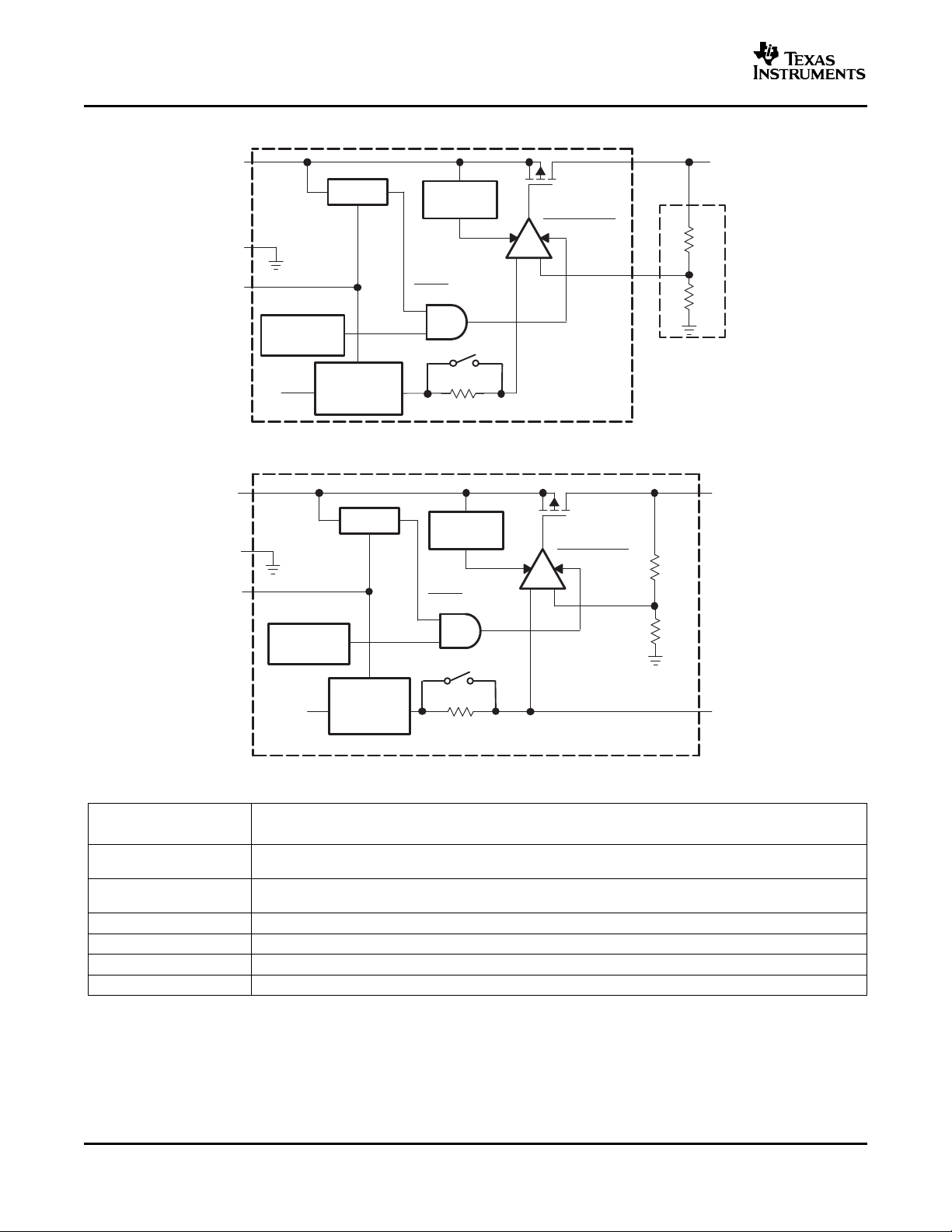
FUNCTIONAL BLOCK DIAGRAM—ADJUSTABLE VERSION
FUNCTIONAL BLOCK DIAGRAM—FIXED VERSION
Table 1. Terminal Functions
TERMINAL
NAME ADJ FIXED
NR N/A 5 Connecting an external capacitor to this pin bypasses noise generated by the internal bandgap. This
EN 1 1 Driving the enable pin (EN) high turns on the regulator. Driving this pin low puts the regulator into shutdown
FB 5 N/A This terminal is the feedback input voltage for the adjustable device.
GND 3, Tab 3, Tab Regulator ground
IN 2 2 Unregulated input to the device.
OUT 4 4 Output of the regulator.
4
improves power-supply rejection and reduces output noise.
mode. EN can be connected to IN if not used.
Submit Documentation Feedback
DESCRIPTION
www.ti.com
2.95
2.96
2.97
2.98
2.99
3.00
3.01
3.02
3.03
3.04
3.05
0.0 0.2 0.4 0.6 0.8 1.0
V
OUT
(V)
I
OUT
(A)
VIN = 4 V
C
OUT
= 10 µF
TJ = 25°C
0
1
2
3
4
−40−25−10 5 20 35 50 65 80 95 110 125
V
OUT
(V)
T
J
(°C)
I
OUT
= 1 mA
2.795
2.790
2.785
2.780
2.775
I
OUT
= 1 A
VIN = 3.8 V
C
OUT
= 10 µF
290
300
310
320
330
340
350
−40−25−10 5 20 35 50 65 80 95 110 125
I
GND
(µA)
TJ (°C)
VIN = 3.8 V
C
OUT
= 10 µF
I
OUT
= 1 mA
I
OUT
= 1 A
0.0
0.1
0.2
0.3
0.4
0.5
0.6
0.7
Frequency (Hz)
100 10k 100k1k
I
OUT
= 1 mA
I
OUT
= 1.5 A
VIN = 5.5 V
C
OUT
= 2.2 µF
CNR = 0.1 µF
Output Spectral Noise Density − µV//Hz
0.0
0.1
0.2
0.3
0.4
0.5
0.6
Frequency (Hz)
100 10k 100k1k
Output Spectral Noise Density − µV//Hz
I
OUT
= 1 mA
I
OUT
= 1 A
VIN = 5.5 V
C
OUT
= 10 µF
CNR = 0.1 µF
0.0
0.5
1.0
1.5
2.0
2.5
Frequency (Hz)
100 10k 100k1k
VIN = 5.5 V
C
OUT
= 10 µF
I
OUT
= 1 A
CNR = 0.1 µF
CNR = 0.01 µF
CNR = 0.0047 µF
CNR = 0.001 µF
Output Spectral Noise Density − µV//Hz
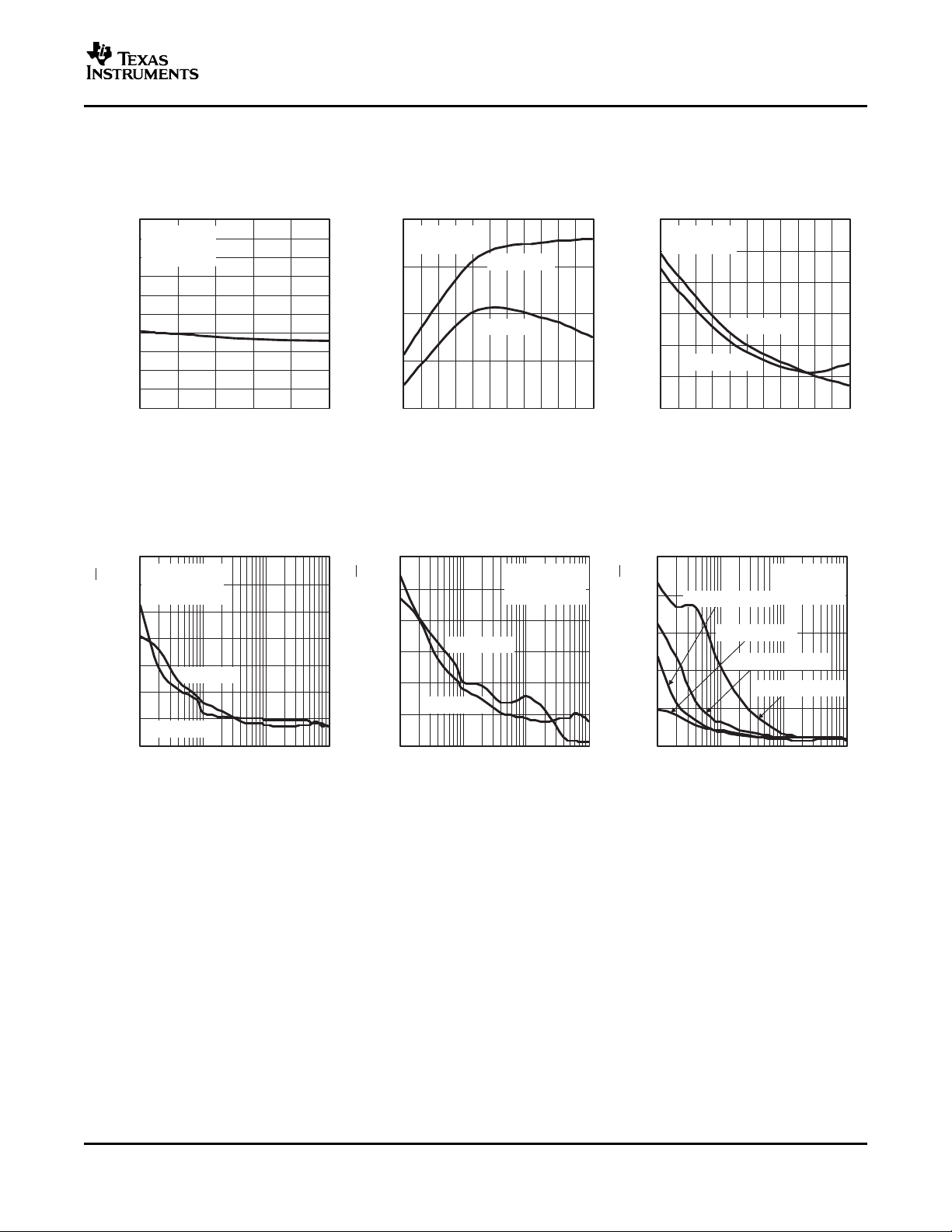
SLVS351I – SEPTEMBER 2002 – REVISED MAY 2006
TYPICAL CHARACTERISTICS
TPS79630 TPS79628 TPS79628
OUTPUT VOLTAGE OUTPUT VOLTAGE GROUND CURRENT
vs vs vs
OUTPUT CURRENT JUNCTION TEMPERATURE JUNCTION TEMPERATURE
Figure 1. Figure 2. Figure 3.
TPS796xx
OUTPUT SPECTRAL NOISE OUTPUT SPECTRAL NOISE OUTPUT SPECTRAL NOISE
TPS79630 TPS79630 TPS79630
DENSITY DENSITY DENSITY
vs vs vs
FREQUENCY FREQUENCY FREQUENCY
Figure 4. Figure 5. Figure 6.
Submit Documentation Feedback
5
www.ti.com
0
50
100
150
200
250
300
350
−40−25−10 5 20 35 50 65 80 95 110 125
V
DO
(mV)
TJ(_C)
VIN= 2.7 V
C
OUT
= 10µF
I
OUT
= 1 A
I
OUT
= 250 mA
0
10
20
30
40
50
60
RMS − Root Mean Squared Output Noise − µV
RMS
CNR (µF)
I
OUT
= 250 mA
C
OUT
= 10 µF
0.001 µF 0.01 µF 0.1 µF0.0047 µF
BW = 100 Hz to 100 kHz
0
10
20
30
40
50
60
70
80
Frequency (Hz)
1 10k 10M1k
Ripple Rejection − dB
I
OUT
= 1 mA
I
OUT
= 1 A
VIN = 4 V
C
OUT
= 10 µF
CNR = 0.01 µF
10 100 100k 1M
0
0.25
0.50
0.75
1
1.25
1.50
1.75
2
2.25
2.50
2.75
3
0 100 200 300 400 500 600
t (ms)
VIN = 4 V,
C
OUT
= 10 µF,
I
OUT
= 1.0 A
Enable
CNR =
0.01 µF
CNR =
0.001 µF
CNR =
0.0047 µF
V
OUT
(V)
0
10
20
30
40
50
60
70
80
Frequency (Hz)
1 10k 10M1k
Ripple Rejection − dB
I
OUT
= 1 mA
I
OUT
= 1 A
VIN = 4 V
C
OUT
= 10 µF
CNR = 0.1 µF
10 100 100k 1M
0
10
20
30
40
50
60
70
80
Frequency (Hz)
1 10k 10M1k
Ripple Rejection − dB
I
OUT
= 1 mA
I
OUT
= 1 A
VIN = 4 V
C
OUT
= 2.2 µF
CNR = 0.01 µF
10 100 100k 1M
0
20
V
IN
(V)
t (µs)
5
4
2
−20
−40
3
40
6040200 80 100 120 140 160 180 200
I
OUT
= 1 A
C
OUT
= 10 µF
CNR = 0.01 µF
dv
dt
+
1 V
ms
∆V
OUT
(mV)
t (µs)
6
5
3
−20
−40
4
0
20
40
6040200 80 100 120 140 160 180 200
I
OUT
= 1 A
C
OUT
= 10 µF
CNR = 0.01 µF
dv
dt
+
1 V
ms
V
IN
(V)∆V
OUT
(mV)
t (µs)
2
1
−1
−75
−150
0
0
75
150
3002001000 400 500 600 700 800 900 1000
VIN = 3.8 V
C
OUT
= 10 µF
CNR = 0.01 µF
di
dt
+
1 A
ms
I
OUT
(A)∆V
OUT
(mV)
TPS796xx
SLVS351I – SEPTEMBER 2002 – REVISED MAY 2006
TYPICAL CHARACTERISTICS (continued)
ROOT MEAN SQUARED OUTPUT TPS79628 TPS79630
TPS79630
NOISE DROPOUT VOLTAGE RIPPLE REJECTION
vs vs vs
BYPASS CAPACITANCE JUNCTION TEMPERATURE FREQUENCY
Figure 7. Figure 8. Figure 9.
TPS79630 TPS79630
RIPPLE REJECTION RIPPLE REJECTION
vs vs
FREQUENCY FREQUENCY START-UP TIME
LINE TRANSIENT RESPONSE LINE TRANSIENT RESPONSE LOAD TRANSIENT RESPONSE
6
Figure 10. Figure 11. Figure 12.
TPS79618 TPS79630 TPS79628
Figure 13. Figure 14. Figure 15.
Submit Documentation Feedback
www.ti.com
0
50
100
150
200
250
300
350
0 100 200 300 400 500 600 700 800 9001000
V
DO
(mV)
I
OUT
(mA)
TJ = 125°C
TJ = −40°C
TJ = 25°C
0
50
100
150
200
250
300
2.5 3.0 3.5 4.0 4.5 5.0
V
DO
(mV)
VIN (V)
TJ = 125°C
TJ = −40°C
TJ = 25°C
I
OUT
= 1 A
C
OUT
= 10 µF
CNR = 0.01 µF
200 µs/Div
4.0
3.5
2.5
0.5
0
3.0
1.0
1.5
2.0
500 mV/Div
3210 4 5 6 7 8 9 10
V
OUT
= 2.5 V
RL = 10 Ω
CNR = 0.01 µF
V
IN
V
OUT
ESR − Equivalent Series Resistance − Ω
I
OUT
(mA)
100
10
1
0.1
0.01
C
OUT
= 10.0 µF
Region of Stability
101 500 750 10006030 250125
Region of
Instability
ESR − Equivalent Series Resistance − Ω
I
OUT
(mA)
Region of
Instability
100
10
1
0.1
0.01
C
OUT
= 1 µF
Region of Stability
101 500 750 10006030 250125
ESR − Equivalent Series Resistance − Ω
I
OUT
(mA)
100
10
1
0.1
0.01
C
OUT
= 2.2 µF
Region of Stability
101 500 750 10006030 250125
Region of
Instability
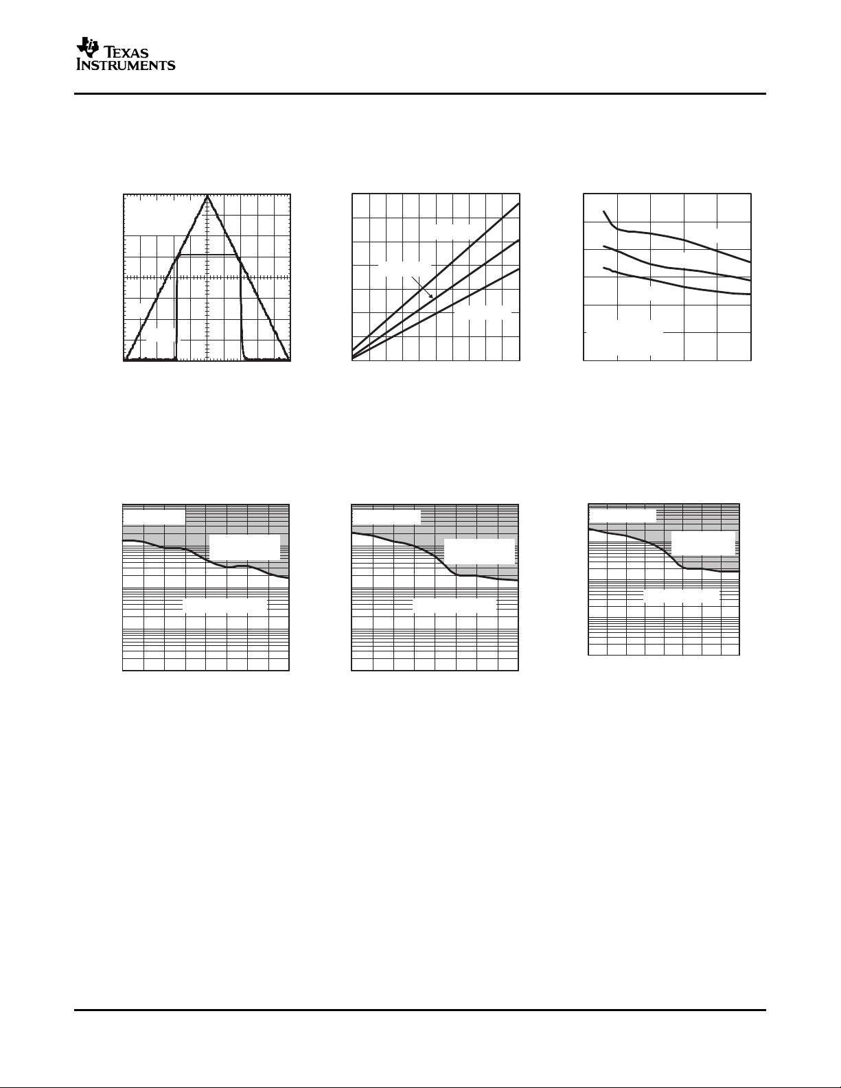
SLVS351I – SEPTEMBER 2002 – REVISED MAY 2006
TYPICAL CHARACTERISTICS (continued)
TPS79630 TPS79601
DROPOUT VOLTAGE DROPOUT VOLTAGE
TPS79625 vs vs
POWER UP/POWER DOWN OUTPUT CURRENT INPUT VOLTAGE
Figure 16. Figure 17. Figure 18.
TPS796xx
TYPICAL REGIONS OF STABILITY TYPICAL REGIONS OF STABILITY TYPICAL REGIONS OF STABILITY
TPS79630 TPS79630 TPS79630
EQUIVALENT SERIES RESISTANCE EQUIVALENT SERIES RESISTANCE EQUIVALENT SERIES RESISTANCE
(ESR) (ESR) (ESR)
vs vs vs
OUTPUT CURRENT OUTPUT CURRENT OUTPUT CURRENT
Figure 19. Figure 20. Figure 21.
Submit Documentation Feedback
7
www.ti.com
GNDEN NR
IN OUT
V
IN
V
OUT
0.01µF
TPS796xx
2.2µF 1 µF
V
OUT
+ V
REF
ǒ
1)
R1
R2
Ǔ
TPS796xx
SLVS351I – SEPTEMBER 2002 – REVISED MAY 2006
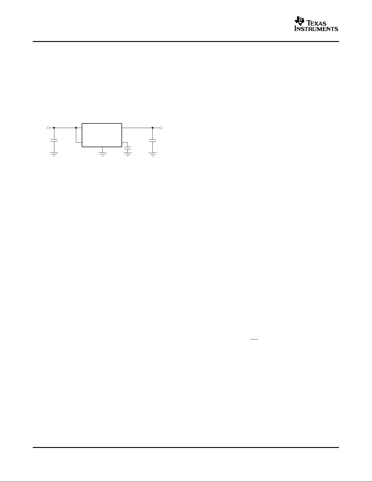
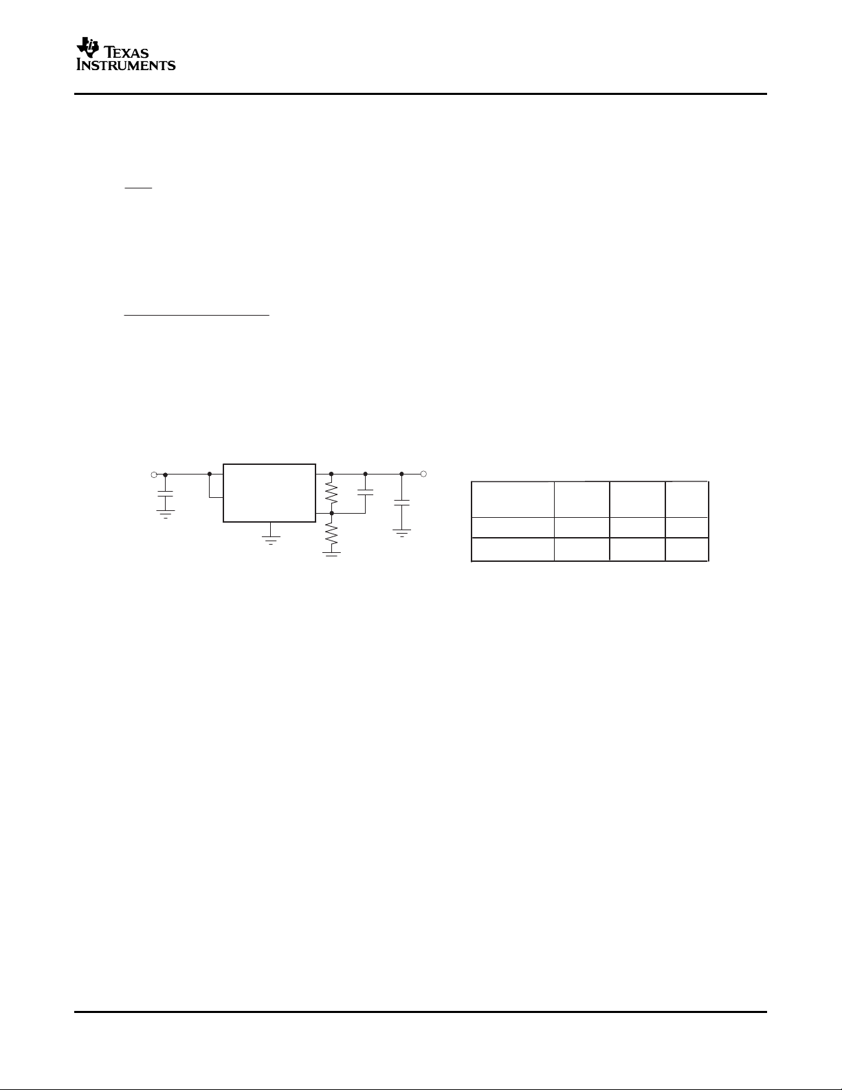
APPLICATION INFORMATION
The TPS796xx family of low-dropout (LDO) For example, the TPS79630 exhibits 40 µ V
regulators has been optimized for use in output voltage noise using a 0.1 µ F ceramic bypass
noise-sensitive equipment. The device features capacitor and a 10 µ F ceramic output capacitor. Note
extremely low dropout voltages, high PSRR, ultralow that the output starts up slower as the bypass
output noise, low quiescent current (265 µ A typically), capacitance increases due to the RC time constant
and enable input to reduce supply currents to less at the bypass pin that is created by the internal
than 1 µ A when the regulator is turned off. 250k Ω resistor and external capacitor.
A typical application circuit is shown in Figure 22 .
Board Layout Recommendation to Improve PSRR and Noise Performance
To improve ac measurements like PSRR, output
noise, and transient response, it is recommended
that the board be designed with separate ground
Figure 22. Typical Application Circuit
External Capacitor Requirements
Although not required, it is good analog design
practice to place a 0.1 µ F — 2.2 µ F capacitor near the
input of the regulator to counteract reactive input
sources. A 2.2 µ F or larger ceramic input bypass
capacitor, connected between IN and GND and
located close to the TPS796xx, is required for
stability and improves transient response, noise
rejection, and ripple rejection. A higher-value input
capacitor may be necessary if large, fast-rise-time
load transients are anticipated and the device is
located several inches from the power source.
Like most low dropout regulators, the TPS796xx
requires an output capacitor connected between
OUT and GND to stabilize the internal control loop.
The minimum recommended capacitor is 1 µ F. Any
1 µ F or larger ceramic capacitor is suitable.
The internal voltage reference is a key source of
noise in an LDO regulator. The TPS796xx has an
NR pin which is connected to the voltage reference
through a 250k Ω internal resistor. The 250k Ω
internal resistor, in conjunction with an external
bypass capacitor connected to the NR pin, creates a
low-pass filter to reduce the voltage reference noise
and, therefore, the noise at the regulator output. In
order for the regulator to operate properly, the
current flow out of the NR pin must be at a minimum,
because any leakage current creates an IR drop
across the internal resistor, thus creating an output
error. Therefore, the bypass capacitor must have
minimal leakage current. The bypass capacitor
should be no more than 0.1 µ F in order to ensure that
it is fully charged during the quickstart time provided
by the internal switch shown in the functional block
diagram.
planes for V
connected only at the ground pin of the device. In
addition, the ground connection for the bypass
capacitor should connect directly to the ground pin of
the device.
Regulator Mounting
The tab of the SOT223-6 package is electrically
connected to ground. For best thermal performance,
the tab of the surface-mount version should be
soldered directly to a circuit-board copper area.
Increasing the copper area improves heat
dissipation.
Solder pad footprint recommendations for the
devices are presented in an application bulletin
Solder Pad Recommendations for Surface-Mount
Devices, literature number AB-132 , available for
download from the TI web site (www.ti.com ).
Programming the TPS79601 Adjustable LDO Regulator
The output voltage of the TPS79601 adjustable
regulator is programmed using an external resistor
divider as shown in Figure 28 . The output voltage is
calculated using Equation 1 :
where:
• V
REF
voltage)
Resistors R1 and R2 should be chosen for
approximately 40 µ A divider current. Lower value
resistors can be used for improved noise
performance, but the device wastes more power.
Higher values should be avoided, as leakage current
at FB increases the output voltage error.
and V
IN
, with each ground plane
OUT
= 1.2246V typ (the internal reference
of
RMS
(1)
8
Submit Documentation Feedback
www.ti.com
R1 +
ǒ
V
OUT
V
REF
*1Ǔ R2
C1 +
(3 x 10⁻⁷) x (R1 ) R2)
(R1 x R2)
OUTPUT VOLTAGE
PROGRAMMING GUIDE
OUTPUT
VOLTAGE
R1 R2 C1
GND
FB
IN OUT
EN
V
IN
V
OUT
R1
C1
R2
TPS79601
1 µF
1.8 V
3.6V
14.0 kΩ
57.9 kΩ
30.1 kΩ
30.1 kΩ
33 pF
15 pF
2.2 µF
TPS796xx
SLVS351I – SEPTEMBER 2002 – REVISED MAY 2006
The recommended design procedure is to choose
R2 = 30.1k Ω to set the divider current at 40 µ A, C1 =
15pF for stability, and then calculate R1 using
Equation 2 :
In order to improve the stability of the adjustable
version, it is suggested that a small compensation
capacitor be placed between OUT and FB. The
approximate value of this capacitor can be calculated
as Equation 3 :
The suggested value of this capacitor for several
resistor ratios is shown in the table below (see
Figure 23 ). If this capacitor is not used (such as in a
unity-gain configuration) then the minimum
recommended output capacitor is 2.2 µ F instead of
1 µ F.
Regulator Protection
The TPS796xx PMOS-pass transistor has a built-in
back diode that conducts reverse current when the
input voltage drops below the output voltage (e.g.,
during power-down). Current is conducted from the
(2)
(3)
output to the input and is not internally limited. If
extended reverse voltage operation is anticipated,
external limiting might be appropriate.
The TPS796xx features internal current limiting and
thermal protection. During normal operation, the
TPS796xx limits output current to approximately
2.8A. When current limiting engages, the output
voltage scales back linearly until the overcurrent
condition ends. While current limiting is designed to
prevent gross device failure, care should be taken
not to exceed the power dissipation ratings of the
package. If the temperature of the device exceeds
approximately +165 ° C, thermal-protection circuitry
shuts it down. Once the device has cooled down to
below approximately +140 ° C, regulator operation
resumes.
Figure 23. TPS79601 Adjustable LDO Regulator Programming
Submit Documentation Feedback
9
www.ti.com
TJ+ TA) PDmax xǒR
θJC
) R
θCS
) R
θSA
Ǔ
PDmax +ǒV
IN(avg)
* V
OUT(avg)
Ǔ
I
OUT(avg))VIN(avg)
I
(Q)
A
B
C
T
J
A
R
θ
JC
T
C
B
R
θ
CS
T
A
C
R
θ
SA
(a)
(b)
DDPAK Package
SOT223 Package
CIRCUIT BOARD COPPER AREA
B
A
C
TPS796xx
SLVS351I – SEPTEMBER 2002 – REVISED MAY 2006
THERMAL INFORMATION
The amount of heat that an LDO linear regulator
generates is directly proportional to the amount of
power it dissipates during operation. All integrated
circuits have a maximum allowable junction
temperature (T
max) above which normal operation
J
is not assured. A system designer must design the
operating environment so that the operating junction
temperature (T
junction temperature (T
) does not exceed the maximum
J
max). The two main
J
environmental variables that a designer can use to
improve thermal performance are air flow and Figure 24 illustrates these thermal resistances for (a)
external heatsinks. The purpose of this information is a SOT223 package mounted in a JEDEC low-K
to aid the designer in determining the proper board, and (b) a DDPAK package mounted on a
operating environment for a linear regulator that is JEDEC high-K board.
operating at a specific power level.
In general, the maximum expected power (P
D(max)
consumed by a linear regulator is computed as
Equation 4 :
(4)
where:
• V
• V
• I
• I
IN(avg)
OUT(avg)
OUT(avg)
is the quiescent current.
(Q)
is the average input voltage.
is the average output voltage.
is the average output current.
For most TI LDO regulators, the quiescent current is
insignificant compared to the average output current;
therefore, the term V
× I
IN(avg)
can be neglected.
(Q)
The operating junction temperature is computed by
adding the ambient temperature (T
) and the
A
increase in temperature due to the regulator's power
dissipation. The temperature rise is computed by
multiplying the maximum expected power dissipation
by the sum of the thermal resistances between the
junction and the case (R
(R
), and the heatsink to ambient (R
θ CS
), the case to heatsink
θ JC
resistances are measures of how effectively an
object dissipates heat. Typically, the larger the
device, the more surface area available for power
dissipation and the lower the object's thermal
resistance.
Equation 5 summarizes the computation:
)
The R
is specific to each regulator as determined
θ JC
by its package, lead frame, and die size provided in
the regulator's data sheet. The R
θ SA
the type and size of heatsink. For example, black
body radiator type heatsinks can have R
ranging from 5 ° C/W for very large heatsinks to
50 ° C/W for very small heatsinks. The R
function of how the package is attached to the
heatsink. For example, if a thermal compound is
used to attach a heatsink to a SOT223 package,
R
of 1 ° C/W is reasonable.
θ CS
). Thermal
θ SA
is a function of
values
θ CS
θ CS
(5)
is a
10
Figure 24. Thermal Resistances
Submit Documentation Feedback

www.ti.com
R
θJA
max + (125 * 55)°Cń2.5 W + 28°CńW
TJ+ TA) PDmax x R
θJA
R
θJA
+
TJ–T
A
PDmax
15
20
25
30
35
40
0.1 1 10 100
Copper Heatsink Area − cm
2
− Thermal Resistance −
θJA
R C/W
°
No Air Flow
150 LFM
250 LFM
1 oz. Copper
Power Plane
1 oz. Copper
Ground Plane
2 oz. Copper Solder Pad
with 25 Thermal Vias
Thermal Vias, 0.3 mm
Diameter, 1,5 mm Pitch
PDmax +(5 * 2.5)V x 1 A + 2.5 W
TPS796xx
SLVS351I – SEPTEMBER 2002 – REVISED MAY 2006
Even if no external black body radiator type heatsink
is attached to the package, the board on which the
regulator is mounted provides some heatsinking
through the pin solder connections. Some packages,
like the DDPAK and SOT223 packages, use a
copper plane underneath the package or the circuit
board's ground plane for additional heatsinking to
improve their thermal performance. Computer-aided
thermal modeling can be used to compute very
accurate approximations of an integrated circuit's
thermal performance in different operating
environments (e.g., different types of circuit boards,
different types and sizes of heatsinks, and different
air flows, etc.). Using these models, the three
thermal resistances can be combined into one
thermal resistance between junction and ambient
(R
). This R
θ JA
is valid only for the specific
θ JA
operating environment used in the computer model.
Equation 5 simplifies into Equation 6 :
Rearranging Equation 6 gives Equation 7 :
Using Equation 6 and the computer model generated
curves shown in Figure 25 and Figure 28 , a designer
can quickly compute the required heatsink thermal
resistance/board area for a given ambient
temperature, power dissipation, and operating
environment.
(9)
From Figure 25 , DDPAK Thermal Resistance vs
Copper Heatsink Area, the ground plane needs to be
2
1cm
for the part to dissipate 2.5W. The operating
environment used in the computer model to construct
Figure 25 consisted of a standard JEDEC High-K
board (2S2P) with a 1-oz. internal copper plane and
ground plane. The package is soldered to a 2-oz.
copper pad. The pad is tied through thermal vias to
the 1-oz. ground plane. Figure 26 shows the side
view of the operating environment used in the
computer model.
(6)
(7)
DDPAK Power Dissipation
The DDPAK package provides an effective means of
managing power dissipation in surface mount
applications. The DDPAK package dimensions are
provided in the Mechanical Data section at the end
of the data sheet. The addition of a copper plane
directly underneath the DDPAK package enhances
the thermal performance of the package.
To illustrate, the TPS72525 in a DDPAK package
was chosen. For this example, the average input
voltage is 5V, the output voltage is 2.5V, the average
output current is 1A, the ambient temperature 55 ° C,
the air flow is 150 LFM, and the operating
environment is the same as documented below.
Neglecting the quiescent current, the maximum
average power is calculated as Equation 8 :
Substituting TJmax for T
Equation 9 :
into Equation 6 gives
J
(8)
Submit Documentation Feedback
Figure 25. DDPAK Thermal Resistance vs Copper
Heatsink Area
Figure 26. DDPAK Thermal Resistance
From the data in Figure 27 and rearranging
Equation 6 , the maximum power dissipation for a
different ground plane area and a specific ambient
temperature can be computed.
11

www.ti.com
0
100
120
140
160
180
PCB Copper Area − in
2
− Thermal Resistance −
θJA
R C/W
°
No Air Flow
80
60
40
20
0.1 1 10
1
2
3
4
5
0.1 1 10 100
Copper Heatsink Area − cm
2
TA = 55°C
No Air Flow
150 LFM
250 LFM
P
D
Maximum (W)
PDmax +(3.3 * 2.5)V x 1 A + 800 mW
R
θJA
max + (125 * 55)°Cń800 mW + 87.5°CńW
0
1
2
3
6
0 25 50 75 100 150125
TA = 25°C
TA (°C)
4
5
4 in2 PCB Area
0.5 in2 PCB Area
P
D
Maximum (W)
TPS796xx
SLVS351I – SEPTEMBER 2002 – REVISED MAY 2006
Figure 27. Maximum Power Dissipation vs
Copper Heatsink Area
SOT223 Power Dissipation
The SOT223 package provides an effective means
of managing power dissipation in surface mount
applications. The SOT223 package dimensions are
provided in the Mechanical Data section at the end
of the data sheet. The addition of a copper plane
directly underneath the SOT223 package enhances
the thermal performance of the package.
To illustrate, the TPS72525 in a SOT223 package
was chosen. For this example, the average input
voltage is 3.3V, the output voltage is 2.5V, the
average output current is 1A, the ambient
temperature 55°C, no air flow is present, and the
operating environment is the same as documented
below. Neglecting the quiescent current, the
maximum average power is calculated as
Equation 10 :
Substituting TJmax for T
Equation 11 :
From Figure 28 , R
ground plane needs to be 0.55in
dissipate 800mW. The operating environment used
to construct Figure 28 consisted of a board with 1-oz.
copper planes. The package is soldered to a 1-oz.
copper pad on the top of the board. The pad is tied
through thermal vias to the 1-oz. ground plane.
12
θ JA
into Equation 6 gives
J
vs PCB Copper Area, the
2
for the part to
Submit Documentation Feedback
Figure 28. SOT223 Thermal Resistance vs PCB
Area
From the data in Figure 28 and rearranging
Equation 6 , the maximum power dissipation for a
different ground plane area and a specific ambient
temperature can be computed (see Figure 29 ).
(10)
(11)
Figure 29. SOT223 Power Dissipation

IMPORTANT NOTICE
Texas Instruments Incorporated and its subsidiaries (TI) reserve the right to make corrections, modifications, enhancements,
improvements, and other changes to its products and services at any time and to discontinue any product or service without notice.
Customers should obtain the latest relevant information before placing orders and should verify that such information is current and
complete. All products are sold subject to TI’s terms and conditions of sale supplied at the time of order acknowledgment.
TI warrants performance of its hardware products to the specifications applicable at the time of sale in accordance with TI’s
standard warranty. Testing and other quality control techniques are used to the extent TI deems necessary to support this
warranty. Except where mandated by government requirements, testing of all parameters of each product is not necessarily
performed.
TI assumes no liability for applications assistance or customer product design. Customers are responsible for their products and
applications using TI components. To minimize the risks associated with customer products and applications, customers should
provide adequate design and operating safeguards.
TI does not warrant or represent that any license, either express or implied, is granted under any TI patent right, copyright, mask
work right, or other TI intellectual property right relating to any combination, machine, or process in which TI products or services
are used. Information published by TI regarding third-party products or services does not constitute a license from TI to use such
products or services or a warranty or endorsement thereof. Use of such information may require a license from a third party under
the patents or other intellectual property of the third party, or a license from TI under the patents or other intellectual property of TI.
Reproduction of information in TI data books or data sheets is permissible only if reproduction is without alteration and is
accompanied by all associated warranties, conditions, limitations, and notices. Reproduction of this information with alteration is an
unfair and deceptive business practice. TI is not responsible or liable for such altered documentation.
Resale of TI products or services with statements different from or beyond the parameters stated by TI for that product or service
voids all express and any implied warranties for the associated TI product or service and is an unfair and deceptive business
practice. TI is not responsible or liable for any such statements.
TI products are not authorized for use in safety-critical applications (such as life support) where a failure of the TI product would
reasonably be expected to cause severe personal injury or death, unless officers of the parties have executed an agreement
specifically governing such use. Buyers represent that they have all necessary expertise in the safety and regulatory ramifications
of their applications, and acknowledge and agree that they are solely responsible for all legal, regulatory and safety-related
requirements concerning their products and any use of TI products in such safety-critical applications, notwithstanding any
applications-related information or support that may be provided by TI. Further, Buyers must fully indemnify TI and its
representatives against any damages arising out of the use of TI products in such safety-critical applications.
TI products are neither designed nor intended for use in military/aerospace applications or environments unless the TI products are
specifically designated by TI as military-grade or "enhanced plastic." Only products designated by TI as military-grade meet military
specifications. Buyers acknowledge and agree that any such use of TI products which TI has not designated as military-grade is
solely at the Buyer's risk, and that they are solely responsible for compliance with all legal and regulatory requirements in
connection with such use.
TI products are neither designed nor intended for use in automotive applications or environments unless the specific TI products
are designated by TI as compliant with ISO/TS 16949 requirements. Buyers acknowledge and agree that, if they use any
non-designated products in automotive applications, TI will not be responsible for any failure to meet such requirements.
Following are URLs where you can obtain information on other Texas Instruments products and application solutions:
Products Applications
Amplifiers amplifier.ti.com Audio www.ti.com/audio
Data Converters dataconverter.ti.com Automotive www.ti.com/automotive
DSP dsp.ti.com Broadband www.ti.com/broadband
Interface interface.ti.com Digital Control www.ti.com/digitalcontrol
Logic logic.ti.com Military www.ti.com/military
Power Mgmt power.ti.com Optical Networking www.ti.com/opticalnetwork
Microcontrollers microcontroller.ti.com Security www.ti.com/security
Low Power www.ti.com/lpw Telephony www.ti.com/telephony
Wireless
Video & Imaging www.ti.com/video
Wireless www.ti.com/wireless
Mailing Address: Texas Instruments, Post Office Box 655303, Dallas, Texas 75265
Copyright © 2007, Texas Instruments Incorporated

PACKAGE OPTION ADDENDUM
www.ti.com
PACKAGING INFORMATION
Orderable Device Status
TPS79601DCQ ACTIVE SOT-223 DCQ 6 78 Green (RoHS &
TPS79601DCQG4 ACTIVE SOT-223 DCQ 6 78 Green (RoHS &
TPS79601DCQR ACTIVE SOT-223 DCQ 6 2500 Green (RoHS &
TPS79601DCQRG4 ACTIVE SOT-223 DCQ 6 2500 Green (RoHS &
TPS79601KTT OBSOLETE DDPAK/
TPS79601KTTR ACTIVE DDPAK/
TPS79601KTTRG3 ACTIVE DDPAK/
TPS79601KTTT ACTIVE DDPAK/
TPS79601KTTTG3 ACTIVE DDPAK/
TPS79613DRBR PREVIEW SON DRB 8 TBD Call TI Call TI
TPS79613DRBT PREVIEW SON DRB 8 TBD Call TI Call TI
TPS79618DCQ ACTIVE SOT-223 DCQ 6 78 Green (RoHS &
TPS79618DCQG4 ACTIVE SOT-223 DCQ 6 78 Green (RoHS &
TPS79618DCQR ACTIVE SOT-223 DCQ 6 2500 Green (RoHS &
TPS79618DCQRG4 ACTIVE SOT-223 DCQ 6 2500 Green (RoHS &
TPS79618KTT OBSOLETE DDPAK/
TPS79618KTTR ACTIVE DDPAK/
TPS79618KTTRG3 ACTIVE DDPAK/
TPS79618KTTT ACTIVE DDPAK/
TPS79618KTTTG3 ACTIVE DDPAK/
TPS79625DCQ ACTIVE SOT-223 DCQ 6 78 Green (RoHS &
TPS79625DCQG4 ACTIVE SOT-223 DCQ 6 78 Green (RoHS &
TPS79625DCQR ACTIVE SOT-223 DCQ 6 2500 Green (RoHS &
TPS79625DCQRG4 ACTIVE SOT-223 DCQ 6 2500 Green (RoHS &
TPS79625KTT OBSOLETE DDPAK/
TPS79625KTTR ACTIVE DDPAK/ KTT 5 500 Green (RoHS & CU SN Level-2-260C-1 YEAR
(1)
Package
Type
TO-263
TO-263
TO-263
TO-263
TO-263
TO-263
TO-263
TO-263
TO-263
TO-263
TO-263
Package
Drawing
KTT 5 TBD Call TI Call TI
KTT 5 500 Green (RoHS &
KTT 5 500 Green (RoHS &
KTT 5 50 Green (RoHS &
KTT 5 50 Green (RoHS &
KTT 5 TBD Call TI Call TI
KTT 5 500 Green (RoHS &
KTT 5 500 Green (RoHS &
KTT 5 50 Green (RoHS &
KTT 5 50 Green (RoHS &
KTT 5 TBD Call TI Call TI
Pins Package
Qty
Eco Plan
no Sb/Br)
no Sb/Br)
no Sb/Br)
no Sb/Br)
no Sb/Br)
no Sb/Br)
no Sb/Br)
no Sb/Br)
no Sb/Br)
no Sb/Br)
no Sb/Br)
no Sb/Br)
no Sb/Br)
no Sb/Br)
no Sb/Br)
no Sb/Br)
no Sb/Br)
no Sb/Br)
no Sb/Br)
no Sb/Br)
(2)
Lead/Ball Finish MSL Peak Temp
CU NIPDAU Level-2-260C-1 YEAR
CU NIPDAU Level-2-260C-1 YEAR
CU NIPDAU Level-2-260C-1 YEAR
CU NIPDAU Level-2-260C-1 YEAR
CU SN Level-2-260C-1 YEAR
CU SN Level-2-260C-1 YEAR
CU SN Level-2-260C-1 YEAR
CU SN Level-2-260C-1 YEAR
CU NIPDAU Level-2-260C-1 YEAR
CU NIPDAU Level-2-260C-1 YEAR
CU NIPDAU Level-2-260C-1 YEAR
CU NIPDAU Level-2-260C-1 YEAR
CU SN Level-2-260C-1 YEAR
CU SN Level-2-260C-1 YEAR
CU SN Level-2-260C-1 YEAR
CU SN Level-2-260C-1 YEAR
CU NIPDAU Level-2-260C-1 YEAR
CU NIPDAU Level-2-260C-1 YEAR
CU NIPDAU Level-2-260C-1 YEAR
CU NIPDAU Level-2-260C-1 YEAR
16-Mar-2007
(3)
Addendum-Page 1

PACKAGE OPTION ADDENDUM
www.ti.com
Orderable Device Status
(1)
Package
Type
Package
Drawing
Pins Package
Qty
Eco Plan
(2)
TO-263 no Sb/Br)
TPS79625KTTRG3 ACTIVE DDPAK/
TO-263
TPS79625KTTT ACTIVE DDPAK/
TO-263
TPS79625KTTTG3 ACTIVE DDPAK/
TO-263
KTT 5 500 Green (RoHS &
no Sb/Br)
KTT 5 50 Green (RoHS &
no Sb/Br)
KTT 5 50 Green (RoHS &
no Sb/Br)
TPS79628DCQ ACTIVE SOT-223 DCQ 6 78 Green (RoHS &
no Sb/Br)
TPS79628DCQG4 ACTIVE SOT-223 DCQ 6 78 Green (RoHS &
no Sb/Br)
TPS79628DCQR ACTIVE SOT-223 DCQ 6 2500 Green (RoHS &
no Sb/Br)
TPS79628DCQRG4 ACTIVE SOT-223 DCQ 6 2500 Green (RoHS &
no Sb/Br)
TPS79628DRBR ACTIVE SON DRB 8 3000 Green (RoHS &
no Sb/Br)
TPS79628DRBRG4 ACTIVE SON DRB 8 3000 Green (RoHS &
no Sb/Br)
TPS79628DRBT ACTIVE SON DRB 8 250 Green (RoHS &
no Sb/Br)
TPS79628DRBTG4 ACTIVE SON DRB 8 250 Green (RoHS &
no Sb/Br)
TPS79628KTT OBSOLETE DDPAK/
KTT 5 TBD Call TI Call TI
TO-263
TPS79628KTTR ACTIVE DDPAK/
TO-263
TPS79628KTTRG3 ACTIVE DDPAK/
TO-263
TPS79628KTTT ACTIVE DDPAK/
TO-263
TPS79628KTTTG3 ACTIVE DDPAK/
TO-263
KTT 5 500 Green (RoHS &
no Sb/Br)
KTT 5 500 Green (RoHS &
no Sb/Br)
KTT 5 50 Green (RoHS &
no Sb/Br)
KTT 5 50 Green (RoHS &
no Sb/Br)
TPS79630DCQ ACTIVE SOT-223 DCQ 6 78 Green (RoHS &
no Sb/Br)
TPS79630DCQG4 ACTIVE SOT-223 DCQ 6 78 Green (RoHS &
no Sb/Br)
TPS79630DCQR ACTIVE SOT-223 DCQ 6 2500 Green (RoHS &
no Sb/Br)
TPS79630DCQRG4 ACTIVE SOT-223 DCQ 6 2500 Green (RoHS &
no Sb/Br)
TPS79630KTT OBSOLETE DDPAK/
KTT 5 TBD Call TI Call TI
TO-263
TPS79630KTTR ACTIVE DDPAK/
TO-263
TPS79630KTTRG3 ACTIVE DDPAK/
TO-263
TPS79630KTTT ACTIVE DDPAK/
TO-263
TPS79630KTTTG3 ACTIVE DDPAK/
TO-263
KTT 5 500 Green (RoHS &
no Sb/Br)
KTT 5 500 Green (RoHS &
no Sb/Br)
KTT 5 50 Green (RoHS &
no Sb/Br)
KTT 5 50 Green (RoHS &
no Sb/Br)
16-Mar-2007
Lead/Ball Finish MSL Peak Temp
CU SN Level-2-260C-1 YEAR
CU SN Level-2-260C-1 YEAR
CU SN Level-2-260C-1 YEAR
CU NIPDAU Level-2-260C-1 YEAR
CU NIPDAU Level-2-260C-1 YEAR
CU NIPDAU Level-2-260C-1 YEAR
CU NIPDAU Level-2-260C-1 YEAR
CU NIPDAU Level-2-260C-1 YEAR
CU NIPDAU Level-2-260C-1 YEAR
CU NIPDAU Level-2-260C-1 YEAR
CU NIPDAU Level-2-260C-1 YEAR
CU SN Level-2-260C-1 YEAR
CU SN Level-2-260C-1 YEAR
CU SN Level-2-260C-1 YEAR
CU SN Level-2-260C-1 YEAR
CU NIPDAU Level-2-260C-1 YEAR
CU NIPDAU Level-2-260C-1 YEAR
CU NIPDAU Level-2-260C-1 YEAR
CU NIPDAU Level-2-260C-1 YEAR
CU SN Level-2-260C-1 YEAR
CU SN Level-2-260C-1 YEAR
CU SN Level-2-260C-1 YEAR
CU SN Level-2-260C-1 YEAR
(3)
Addendum-Page 2

PACKAGE OPTION ADDENDUM
www.ti.com
Orderable Device Status
(1)
Package
Type
Package
Drawing
Pins Package
Qty
Eco Plan
TPS79633DCQ ACTIVE SOT-223 DCQ 6 78 Green (RoHS &
(2)
Lead/Ball Finish MSL Peak Temp
CU NIPDAU Level-2-260C-1 YEAR
16-Mar-2007
(3)
no Sb/Br)
TPS79633DCQG4 ACTIVE SOT-223 DCQ 6 78 Green (RoHS &
CU NIPDAU Level-2-260C-1 YEAR
no Sb/Br)
TPS79633DCQR ACTIVE SOT-223 DCQ 6 2500 Green (RoHS &
CU NIPDAU Level-2-260C-1 YEAR
no Sb/Br)
TPS79633DCQRG4 ACTIVE SOT-223 DCQ 6 2500 Green (RoHS &
CU NIPDAU Level-2-260C-1 YEAR
no Sb/Br)
TPS79633KTT OBSOLETE DDPAK/
KTT 5 TBD Call TI Call TI
TO-263
TPS79633KTTR ACTIVE DDPAK/
TO-263
TPS79633KTTRG3 ACTIVE DDPAK/
TO-263
TPS79633KTTT ACTIVE DDPAK/
TO-263
TPS79633KTTTG3 ACTIVE DDPAK/
TO-263
TPS79650DCQ ACTIVE SOT-223 DCQ 6 78 Green (RoHS &
KTT 5 500 Green (RoHS &
no Sb/Br)
KTT 5 500 Green (RoHS &
no Sb/Br)
KTT 5 50 Green (RoHS &
no Sb/Br)
KTT 5 50 Green (RoHS &
no Sb/Br)
CU SN Level-2-260C-1 YEAR
CU SN Level-2-260C-1 YEAR
CU SN Level-2-260C-1 YEAR
CU SN Level-2-260C-1 YEAR
CU NIPDAU Level-2-260C-1 YEAR
no Sb/Br)
TPS79650DCQG4 ACTIVE SOT-223 DCQ 6 78 Green (RoHS &
CU NIPDAU Level-2-260C-1 YEAR
no Sb/Br)
TPS79650DCQR ACTIVE SOT-223 DCQ 6 2500 Green (RoHS &
CU NIPDAU Level-2-260C-1 YEAR
no Sb/Br)
TPS79650DCQRG4 ACTIVE SOT-223 DCQ 6 2500 Green (RoHS &
CU NIPDAU Level-2-260C-1 YEAR
no Sb/Br)
TPS79650DRBR ACTIVE SON DRB 8 3000 Green (RoHS &
CU NIPDAU Level-2-260C-1 YEAR
no Sb/Br)
TPS79650DRBRG4 ACTIVE SON DRB 8 3000 Green (RoHS &
CU NIPDAU Level-2-260C-1 YEAR
no Sb/Br)
TPS79650DRBT ACTIVE SON DRB 8 250 Green (RoHS &
CU NIPDAU Level-2-260C-1 YEAR
no Sb/Br)
TPS79650DRBTG4 ACTIVE SON DRB 8 250 Green (RoHS &
CU NIPDAU Level-2-260C-1 YEAR
no Sb/Br)
(1)
The marketing status values are defined as follows:
ACTIVE: Product device recommended for new designs.
LIFEBUY: TI has announced that the device will be discontinued, and a lifetime-buy period is in effect.
NRND: Not recommended for new designs. Device is in production to support existing customers, but TI does not recommend using this part in
a new design.
PREVIEW: Device has been announced but is not in production. Samples may or may not be available.
OBSOLETE: TI has discontinued the production of the device.
(2)
Eco Plan - The planned eco-friendly classification: Pb-Free (RoHS), Pb-Free (RoHS Exempt), or Green (RoHS & no Sb/Br) - please check
http://www.ti.com/productcontent for the latest availability information and additional product content details.
TBD: The Pb-Free/Green conversion plan has not been defined.
Pb-Free (RoHS): TI's terms "Lead-Free" or "Pb-Free" mean semiconductor products that are compatible with the current RoHS requirements
for all 6 substances, including the requirement that lead not exceed 0.1% by weight in homogeneous materials. Where designed to be soldered
at high temperatures, TI Pb-Free products are suitable for use in specified lead-free processes.
Pb-Free (RoHS Exempt): This component has a RoHS exemption for either 1) lead-based flip-chip solder bumps used between the die and
package, or 2) lead-based die adhesive used between the die and leadframe. The component is otherwise considered Pb-Free (RoHS
compatible) as defined above.
Green (RoHS & no Sb/Br): TI defines "Green" to mean Pb-Free (RoHS compatible), and free of Bromine (Br) and Antimony (Sb) based flame
retardants (Br or Sb do not exceed 0.1% by weight in homogeneous material)
Addendum-Page 3

PACKAGE OPTION ADDENDUM
www.ti.com
(3)
MSL, Peak Temp. -- The Moisture Sensitivity Level rating according to the JEDEC industry standard classifications, and peak solder
temperature.
Important Information and Disclaimer:The information provided on this page represents TI's knowledge and belief as of the date that it is
provided. TI bases its knowledge and belief on information provided by third parties, and makes no representation or warranty as to the
accuracy of such information. Efforts are underway to better integrate information from third parties. TI has taken and continues to take
reasonable steps to provide representative and accurate information but may not have conducted destructive testing or chemical analysis on
incoming materials and chemicals. TI and TI suppliers consider certain information to be proprietary, and thus CAS numbers and other limited
information may not be available for release.
In no event shall TI's liability arising out of such information exceed the total purchase price of the TI part(s) at issue in this document sold by TI
to Customer on an annual basis.
16-Mar-2007
Addendum-Page 4

PACKAGE MATERIALS INFORMATION
www.ti.com
15-May-2007
TAPE AND REEL INFORMATION
Pack Materials-Page 1

PACKAGE MATERIALS INFORMATION
www.ti.com
Device Package Pins Site Reel
Diameter
(mm)
TPS79601DCQR DCQ 6 HNT 330 8 6.8 7.3 1.88 8 12 Q3
TPS79618DCQR DCQ 6 HNT 330 8 6.8 7.3 1.88 8 12 Q3
TPS79625DCQR DCQ 6 HNT 330 8 6.8 7.3 1.88 8 12 Q3
TPS79628DCQR DCQ 6 HNT 330 8 6.8 7.3 1.88 8 12 Q3
TPS79628DRBR DRB 8 MLA 330 12 3.3 3.3 1.1 8 12 Q2
TPS79628DRBT DRB 8 MLA 180 12 3.3 3.3 1.1 8 12 Q2
TPS79630DCQR DCQ 6 HNT 330 8 6.8 7.3 1.88 8 12 Q3
TPS79633DCQR DCQ 6 HNT 330 8 6.8 7.3 1.88 8 12 Q3
TPS79650DCQR DCQ 6 HNT 330 8 6.8 7.3 1.88 8 12 Q3
TPS79650DRBR DRB 8 MLA 330 12 3.3 3.3 1.1 8 12 Q2
TPS79650DRBT DRB 8 MLA 180 12 3.3 3.3 1.1 8 12 Q2
Reel
Width
(mm)
A0 (mm) B0 (mm) K0 (mm) P1
(mm)W(mm)
15-May-2007
Pin1
Quadrant
TAPE AND REEL BOX INFORMATION
Device Package Pins Site Length (mm) Width (mm) Height (mm)
TPS79601DCQR DCQ 6 HNT 358.0 335.0 35.0
TPS79618DCQR DCQ 6 HNT 358.0 335.0 35.0
TPS79625DCQR DCQ 6 HNT 358.0 335.0 35.0
TPS79628DCQR DCQ 6 HNT 358.0 335.0 35.0
TPS79628DRBR DRB 8 MLA 346.0 346.0 29.0
TPS79628DRBT DRB 8 MLA 190.0 212.7 31.75
TPS79630DCQR DCQ 6 HNT 358.0 335.0 35.0
TPS79633DCQR DCQ 6 HNT 358.0 335.0 35.0
TPS79650DCQR DCQ 6 HNT 358.0 335.0 35.0
TPS79650DRBR DRB 8 MLA 346.0 346.0 29.0
Pack Materials-Page 2

PACKAGE MATERIALS INFORMATION
www.ti.com
Device Package Pins Site Length (mm) Width (mm) Height (mm)
TPS79650DRBT DRB 8 MLA 190.0 212.7 31.75
15-May-2007
Pack Materials-Page 3


IMPORTANT NOTICE
Texas Instruments Incorporated and its subsidiaries (TI) reserve the right to make corrections, modifications, enhancements,
improvements, and other changes to its products and services at any time and to discontinue any product or service without notice.
Customers should obtain the latest relevant information before placing orders and should verify that such information is current and
complete. All products are sold subject to TI’s terms and conditions of sale supplied at the time of order acknowledgment.
TI warrants performance of its hardware products to the specifications applicable at the time of sale in accordance with TI’s
standard warranty. Testing and other quality control techniques are used to the extent TI deems necessary to support this
warranty. Except where mandated by government requirements, testing of all parameters of each product is not necessarily
performed.
TI assumes no liability for applications assistance or customer product design. Customers are responsible for their products and
applications using TI components. To minimize the risks associated with customer products and applications, customers should
provide adequate design and operating safeguards.
TI does not warrant or represent that any license, either express or implied, is granted under any TI patent right, copyright, mask
work right, or other TI intellectual property right relating to any combination, machine, or process in which TI products or services
are used. Information published by TI regarding third-party products or services does not constitute a license from TI to use such
products or services or a warranty or endorsement thereof. Use of such information may require a license from a third party under
the patents or other intellectual property of the third party, or a license from TI under the patents or other intellectual property of TI.
Reproduction of information in TI data books or data sheets is permissible only if reproduction is without alteration and is
accompanied by all associated warranties, conditions, limitations, and notices. Reproduction of this information with alteration is an
unfair and deceptive business practice. TI is not responsible or liable for such altered documentation.
Resale of TI products or services with statements different from or beyond the parameters stated by TI for that product or service
voids all express and any implied warranties for the associated TI product or service and is an unfair and deceptive business
practice. TI is not responsible or liable for any such statements.
TI products are not authorized for use in safety-critical applications (such as life support) where a failure of the TI product would
reasonably be expected to cause severe personal injury or death, unless officers of the parties have executed an agreement
specifically governing such use. Buyers represent that they have all necessary expertise in the safety and regulatory ramifications
of their applications, and acknowledge and agree that they are solely responsible for all legal, regulatory and safety-related
requirements concerning their products and any use of TI products in such safety-critical applications, notwithstanding any
applications-related information or support that may be provided by TI. Further, Buyers must fully indemnify TI and its
representatives against any damages arising out of the use of TI products in such safety-critical applications.
TI products are neither designed nor intended for use in military/aerospace applications or environments unless the TI products are
specifically designated by TI as military-grade or "enhanced plastic." Only products designated by TI as military-grade meet military
specifications. Buyers acknowledge and agree that any such use of TI products which TI has not designated as military-grade is
solely at the Buyer's risk, and that they are solely responsible for compliance with all legal and regulatory requirements in
connection with such use.
TI products are neither designed nor intended for use in automotive applications or environments unless the specific TI products
are designated by TI as compliant with ISO/TS 16949 requirements. Buyers acknowledge and agree that, if they use any
non-designated products in automotive applications, TI will not be responsible for any failure to meet such requirements.
Following are URLs where you can obtain information on other Texas Instruments products and application solutions:
Products Applications
Amplifiers amplifier.ti.com Audio www.ti.com/audio
Data Converters dataconverter.ti.com Automotive www.ti.com/automotive
DSP dsp.ti.com Broadband www.ti.com/broadband
Interface interface.ti.com Digital Control www.ti.com/digitalcontrol
Logic logic.ti.com Military www.ti.com/military
Power Mgmt power.ti.com Optical Networking www.ti.com/opticalnetwork
Microcontrollers microcontroller.ti.com Security www.ti.com/security
RFID www.ti-rfid.com Telephony www.ti.com/telephony
Low Power www.ti.com/lpw Video & Imaging www.ti.com/video
Wireless
Wireless www.ti.com/wireless
Mailing Address: Texas Instruments, Post Office Box 655303, Dallas, Texas 75265
Copyright © 2007, Texas Instruments Incorporated
 Loading...