

Texas Instruments TPS77333DGKR, TPS77333DGK, TPS77328DGKR, TPS77328DGK, TPS77327DGKR Datasheet
...
TPS77301, TPS77318, TPS77327, TPS77328, TPS77333 WITH RESET OUTPUT
TPS77401, TPS77418, TPS77427, TPS77428, TPS77433 WITH POWER GOOD OUTPUT
250-mA LDO REGULATORS WITH INTEGRATED RESET OR PG
SLVS281A – FEBRUARY 2000 – REVISED MARCH 2000
D
Open Drain Power-On Reset With 220-ms
Delay (TPS773xx)
D
Open Drain Power-Good (PG) Status
Output (TPS774xx)
D
250-mA Low-Dropout Voltage Regulator
D
Available in 1.8-V, 2.7-V, 2.8-V, 3.3-V, Fixed
Output and Adjustable Versions
D
Dropout Voltage Typically 200 mV
at 250 mA (TPS77333, TPS77433)
D
Ultra Low 92-µA Quiescent Current (Typ)
D
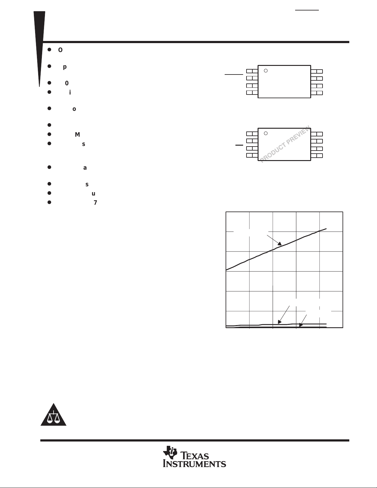
8-Pin MSOP (DGK) Package
D
Low Noise (55 µV
) Without an External
rms
Filter (Bypass) Capacitor (TPS77318,
TPS77418)
D
2% Tolerance Over Specified Conditions
For Fixed-Output Versions
D
Fast Transient Response
D
Thermal Shutdown Protection
D
See the TPS779xx Family of Devices for
Active High Enable
FB/SENSE
RESET
EN
GND
FB/SENSE
PG
EN
GND
300
TPS773xx
DGK PACKAGE
(TOP VIEW)
1
2
3
4
TPS774xx
DGK PACKAGE
(TOP VIEW)
1
2
3
4
TPS77x33
DROPOUT VOLTAGE
vs
JUNCTION TEMPERATURE
8
7
6
5
8
7
6
5
OUT
OUT
IN
IN
OUT
OUT
IN
IN
description
250
IO = 250 mA
The TPS773xx and TPS774xx are low dropout
regulators with integrated power-on reset and
power good (PG) function respectively. These
200
devices are capable of supplying 250 mA of output
current with a dropout of 200 mV (TPS77333,
150
TPS77433). Quiescent current is 92 µA at full load
dropping down to 1 µA when device is disabled.
– Dropout Voltage – mV
These devices are optimized to be stable with a
wide range of output capacitors including low ESR
ceramic (10 µF) or low capacitance (1 µF)
tantalum capacitors. These devices have extremely low noise output performance (55 µV
rms
without using any added filter capacitors.
TPS773xx and TPS774xx are designed to have
fast transient response for larger load current
)
100
DO
V
50
0
–40 0 40 80
TJ – Junction Temperature – °C
IO = 10 mA
IO = 0 A
changes.
The TPS773xx or TPS774xx is offered in 1.8-V, 2.7-V, 2.8-V and 3.3-V fixed-voltage versions and in an
adjustable version (programmable over the range of 1.5 V to 5.5 V). Output voltage tolerance is 2% over line,
load, and temperature ranges. The TPS773xx and TPS774xx families are available in 8-pin MSOP (DGK)
packages.
120 140
Please be aware that an important notice concerning availability, standard warranty, and use in critical applications of
Texas Instruments semiconductor products and disclaimers thereto appears at the end of this data sheet.
This document contains information on products in more than one phase
of development. The status of each device is indicated on the page(s)
specifying its electrical characteristics.
POST OFFICE BOX 655303 • DALLAS, TEXAS 75265
Copyright 2000, Texas Instruments Incorporated
1
TPS77301, TPS77318, TPS77327, TPS77328, TPS77333 WITH RESET OUTPUT
J
–40 C to 125 C
TPS77401, TPS77418, TPS77427, TPS77428, TPS77433 WITH POWER GOOD OUTPUT
250-mA LDO REGULATORS WITH INTEGRATED RESET OR PG
SLVS281A – FEBRUARY 2000 – REVISED MARCH 2000
description (continued)
Because the PMOS device behaves as a low-value resistor, the dropout voltage is very low (typically 200 mV
at an output current of 250 mA for 3.3 volt option) and is directly proportional to the output current. Additionally ,
since the PMOS pass element is a voltage-driven device, the quiescent current is very low and independent
of output loading (typically 92 µA over the full range of output current, 0 mA to 250 mA). These two key
specifications yield a significant improvement in operating life for battery-powered systems.
The device is enabled when the EN
pin is connected to a low-level input voltage. This LDO family also features
a sleep mode; applying a TTL high signal to EN (enable) shuts down the regulator, reducing the quiescent
current to less than 1 µA at TJ = 25°C.
The TPS773xx features an integrated power-on reset, commonly used as an supply voltage supervisor (SVS),
or reset output voltage. The RESET output of the TPS773xx initiates a reset in DSP, microcomputer or
microprocessor systems at power-up and in the event of an undervoltage condition. An internal comparator in
the TPS773xx monitors the output voltage of the regulator to detect an undervoltage condition on the regulated
output voltage. When OUT
reaches 95% of its regulated voltage, RESET will go to a high-impedance state after
a 220 ms delay . RESET will go to low-impedance state when OUT is pulled below 95% (i.e. over load condition)
of its regulated voltage.
For the TPS774xx, the power good terminal (PG) is an active high output, which can be used to implement a
power-on reset or a low-battery indicator. An internal comparator in the TPS774xx monitors the output voltage
of the regulator to detect an undervoltage condition on the regulated output voltage. When OUT falls below 82%
of its regulated voltage, PG will go to a low-impedance state. PG will go to a high-impedance state when OUT
is above 82% of its regulated voltage.
AVAILABLE OPTIONS
OUTPUT
VOLTAGE
T
–
°
The TPS77301 and TPS77401 are programmable using an external resistor divider
(see application information). The DGK package is available taped and reeled. Add
an R suffix to the device type (e.g., TPS77301DGKR).
°
(V)
TYP
3.3 TPS77333DGK TPS77433DGK
2.8 TPS77328DGK TPS77428DGK
2.7 TPS77327DGK TPS77427DGK
1.8 TPS77318DGK TPS77418DGK
Adjustable
1.5 V to 5.5 V
PACKAGED DEVICES
MSOP
(DGK)
TPS77301DGK TPS77401DGK
2
POST OFFICE BOX 655303 • DALLAS, TEXAS 75265
TPS77301, TPS77318, TPS77327, TPS77328, TPS77333 WITH RESET OUTPUT
TPS77401, TPS77418, TPS77427, TPS77428, TPS77433 WITH POWER GOOD OUTPUT
250-mA LDO REGULATORS WITH INTEGRATED RESET OR PG
SLVS281A – FEBRUARY 2000 – REVISED MARCH 2000
V
I
0.1 µF
5
6
3
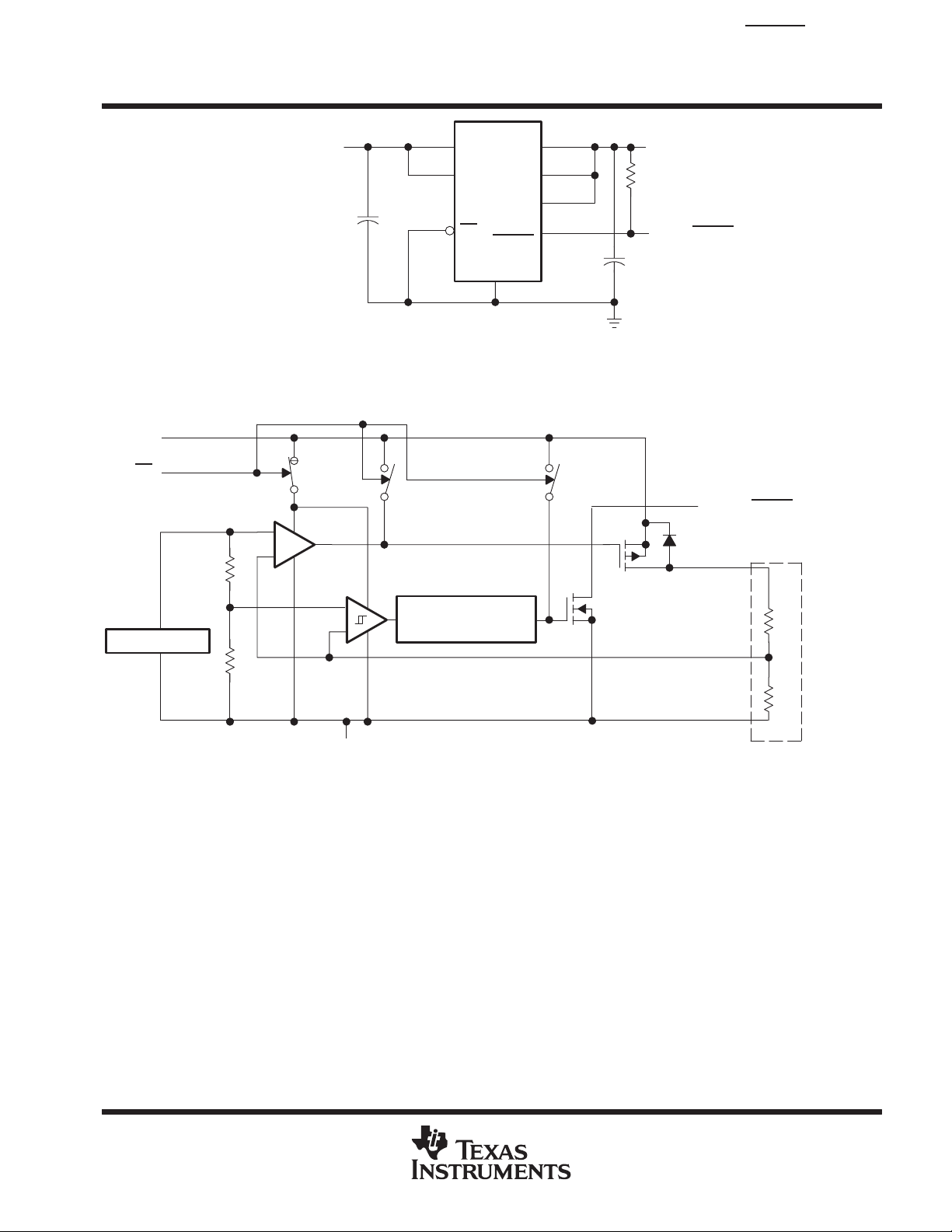
Figure 1. Typical Application Configuration (For Fixed Output Options)
functional block diagram—adjustable version
IN
EN
_
+
IN
IN
EN
GND
4
OUT
OUT
SENSE
PG or
RESET
7
8
1
2
V
O
PG or RESET Output
+
10 µF
PG or RESET
OUT
V
= 1.1834 V
ref
GND
+
_
220 ms Delay
(for TPS773xx Option)
R1
FB/SENSE
R2
External to the device
POST OFFICE BOX 655303 • DALLAS, TEXAS 75265
3
TPS77301, TPS77318, TPS77327, TPS77328, TPS77333 WITH RESET OUTPUT
I/O
DESCRIPTION
I/O
DESCRIPTION
TPS77401, TPS77418, TPS77427, TPS77428, TPS77433 WITH POWER GOOD OUTPUT
250-mA LDO REGULATORS WITH INTEGRATED RESET OR PG
SLVS281A – FEBRUARY 2000 – REVISED MARCH 2000
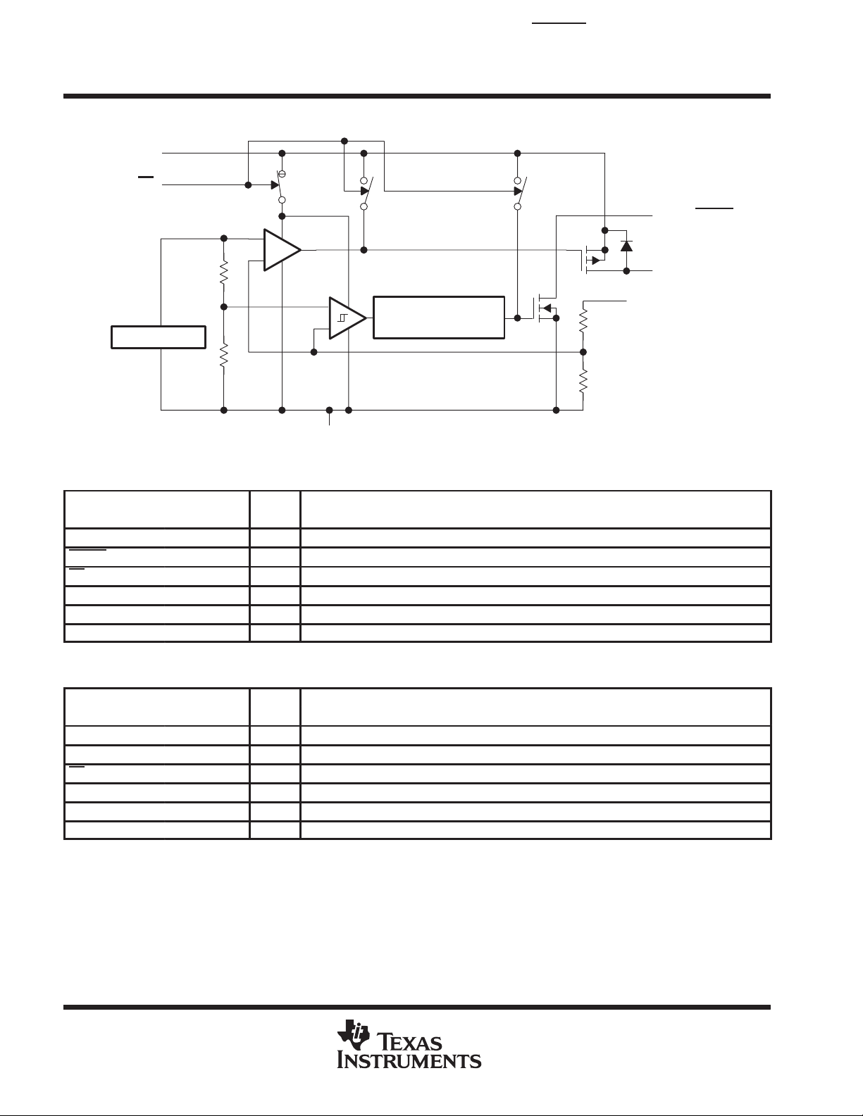
functional block diagram—fixed-voltage version
IN
EN
PG or RESET
_
V
= 1.1834 V
ref
+
+
_
GND
220 ms Delay
(for TPS773xx Option)
R1
R2
OUT
SENSE
Terminal Functions (TPS773xx)
TERMINAL
NAME NO.
FB/SENSE 1 I Feedback input voltage for adjustable device (sense input for fixed options)
RESET 2 O Reset output
EN 3 I Enable input
GND 4 Regulator ground
IN 5, 6 I Input voltage
OUT 7, 8 O Regulated output voltage
Terminal Functions (TPS774xx)
TERMINAL
NAME NO.
FB/SENSE 1 I Feedback input voltage for adjustable device (sense input for fixed options)
PG 2 O Power good
EN 3 I Enable input
GND 4 Regulator ground
IN 5, 6 I Input voltage
OUT 7, 8 O Regulated output voltage
4
POST OFFICE BOX 655303 • DALLAS, TEXAS 75265
TPS77301, TPS77318, TPS77327, TPS77328, TPS77333 WITH RESET OUTPUT
TPS77401, TPS77418, TPS77427, TPS77428, TPS77433 WITH POWER GOOD OUTPUT
250-mA LDO REGULATORS WITH INTEGRATED RESET OR PG
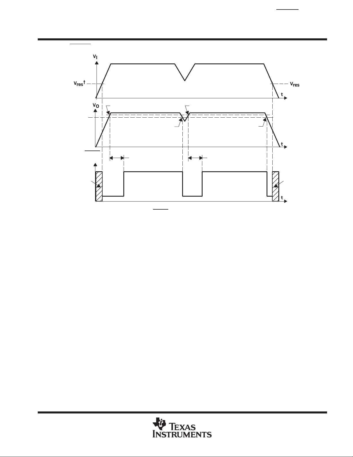
TPS773xx RESET timing diagram
V
I
†
V
res
SLVS281A – FEBRUARY 2000 – REVISED MARCH 2000
V
res
t
V
O
Threshold
Voltage
RESET
Output
Output
Undefined
†
V
is the minimum input voltage for a valid RESET . The symbol V
res
for semiconductor symbology.
‡
VIT –Trip voltage is typically 5% lower than the output voltage (95%VO) V
to V
is the hysteresis voltage.
IT+
V
IT+
‡
220 ms
Delay
V
IT+
‡
V
IT–
res
‡
‡
V
IT–
t
220 ms
Delay
Output
Undefined
t
is not currently listed within EIA or JEDEC standards
IT–
POST OFFICE BOX 655303 • DALLAS, TEXAS 75265
5
TPS77301, TPS77318, TPS77327, TPS77328, TPS77333 WITH RESET OUTPUT
TPS77401, TPS77418, TPS77427, TPS77428, TPS77433 WITH POWER GOOD OUTPUT
250-mA LDO REGULATORS WITH INTEGRATED RESET OR PG
SLVS281A – FEBRUARY 2000 – REVISED MARCH 2000
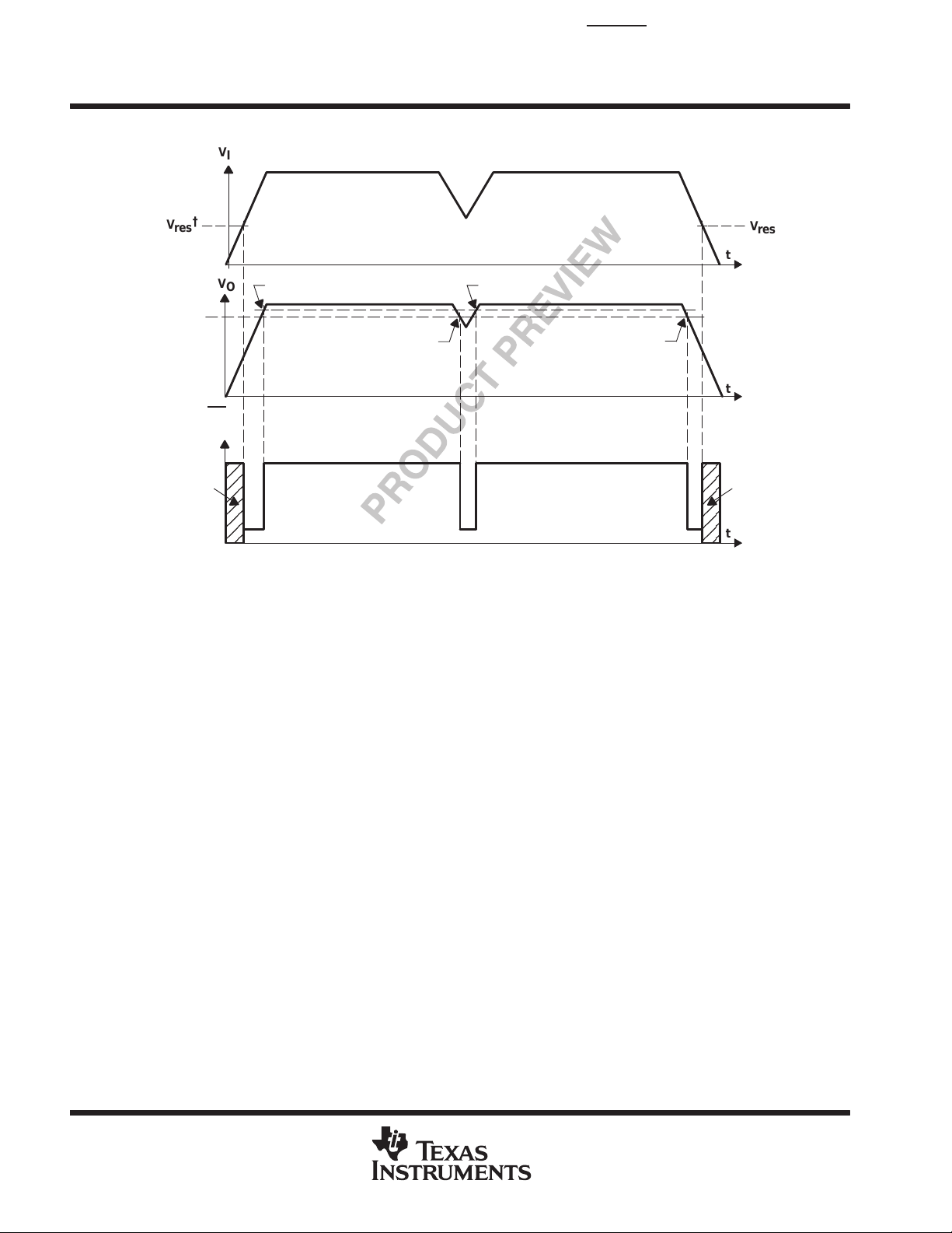
TPS774xx PG timing diagram
V
I
†
V
res
V
res
t
V
O
Threshold
Voltage
PG
Output
Output
Undefined
†
V
is the minimum input voltage for a valid PG. The symbol V
res
semiconductor symbology .
‡
VIT –Trip voltage is typically 18% lower than the output voltage (82%VO) V
to V
is the hysteresis voltage.
IT+
‡
V
IT+
‡
V
IT–
V
IT+
is not currently listed within EIA or JEDEC standards for
res
‡
‡
V
IT–
t
Output
Undefined
t
IT–
6
POST OFFICE BOX 655303 • DALLAS, TEXAS 75265
TPS77301, TPS77318, TPS77327, TPS77328, TPS77333 WITH RESET OUTPUT
TPS77401, TPS77418, TPS77427, TPS77428, TPS77433 WITH POWER GOOD OUTPUT
250-mA LDO REGULATORS WITH INTEGRATED RESET OR PG
SLVS281A – FEBRUARY 2000 – REVISED MARCH 2000
absolute maximum ratings over operating junction temperature range
(unless otherwise noted)
Input voltage range‡, VI –0.3 V to 13.5 V. . . . . . . . . . . . . . . . . . . . . . . . . . . . . . . . . . . . . . . . . . . . . . . . . . . . . . . . . .
Voltage range at EN –0.3 V to 16.5 V. . . . . . . . . . . . . . . . . . . . . . . . . . . . . . . . . . . . . . . . . . . . . . . . . . . . . . . . . . . . . .
Maximum RESET voltage (TPS773xx) 16.5 V. . . . . . . . . . . . . . . . . . . . . . . . . . . . . . . . . . . . . . . . . . . . . . . . . . . . . .
Maximum PG voltage (TPS774xx) 16.5 V. . . . . . . . . . . . . . . . . . . . . . . . . . . . . . . . . . . . . . . . . . . . . . . . . . . . . . . . .
Peak output current Internally limited. . . . . . . . . . . . . . . . . . . . . . . . . . . . . . . . . . . . . . . . . . . . . . . . . . . . . . . . . . . . . .
Continuous total power dissipation See dissipation rating tables. . . . . . . . . . . . . . . . . . . . . . . . . . . . . . . . . . . . . .
Output voltage, V
Operating virtual junction temperature range, TJ –40°C to 125°C. . . . . . . . . . . . . . . . . . . . . . . . . . . . . . . . . . . . .
Storage temperature range, T
ESD rating, HBM 2 kV. . . . . . . . . . . . . . . . . . . . . . . . . . . . . . . . . . . . . . . . . . . . . . . . . . . . . . . . . . . . . . . . . . . . . . . . . .
†
Stresses beyond those listed under “absolute maximum ratings” may cause permanent damage to the device. These are stress ratings only, and
functional operation of the device at these or any other conditions beyond those indicated under “recommended operating conditions” is not
implied. Exposure to absolute-maximum-rated conditions for extended periods may affect device reliability.
‡
All voltage values are with respect to network terminal ground.
PACKAGE
DGK
(OUT, FB) 5.5 V. . . . . . . . . . . . . . . . . . . . . . . . . . . . . . . . . . . . . . . . . . . . . . . . . . . . . . . . . . . . . .
O
–65°C to 150°C. . . . . . . . . . . . . . . . . . . . . . . . . . . . . . . . . . . . . . . . . . . . . . . . . . .
stg
DISSIPATION RATING TABLE – FREE-AIR TEMPERATURES
AIR FLOW
(CFM)
0 266.2 3.84 376 mW 3.76 mW/°C 207 mW 150 mW
150 255.2 3.92 392 mW 3.92 mW/°C 216 mW 157 mW
250 242.8 4.21 412 mW 4.12 mW/°C 227 mW 165 mW
θ
JA
(°C/W)
θ
JC
(°C/W)
TA < 25°C
POWER RATING
DERATING FACTOR
ABOVE TA = 25°C
Ĕ
TA = 70°C
POWER RATING
TA = 85°C
POWER RATING
recommended operating conditions
MIN MAX UNIT
Input voltage, V
Output voltage range, V
Output current, IO (see Note 1) 0 250 mA
Operating virtual junction temperature, TJ (see Note 1) –40 125 °C
§
To calculate the minimum input voltage for your maximum output current, use the following equation: V
NOTE 1: Continuous current and operating junction temperature are limited by internal protection circuitry, but it is not recommended that the
§
I
O
I(min)
device operate under conditions beyond those specified in this table for extended periods of time.
= V
2.7 10 V
1.5 5.5 V
+ V
O(max)
DO(max load)
.
POST OFFICE BOX 655303 • DALLAS, TEXAS 75265
7

TPS77301, TPS77318, TPS77327, TPS77328, TPS77333 WITH RESET OUTPUT
j
1.8 V Output
Output voltage (see Notes 2 and 4)
2.7 V Output
V
2.8 V Output
3.3 V Output
Quiescent current (GND current) (see Notes 2 and 4)
A
Output voltage line regulation (∆VO/VO)(see Note 3)
Standby current
PG
(
)
(TPS774xx)
TPS77401, TPS77418, TPS77427, TPS77428, TPS77433 WITH POWER GOOD OUTPUT
250-mA LDO REGULATORS WITH INTEGRATED RESET OR PG
SLVS281A – FEBRUARY 2000 – REVISED MARCH 2000
electrical characteristics over recommended operating junction temperature range (TJ = –40°C to
125°C), V
p
p
Load regulation TJ = 25°C 1 mV
Output noise voltage
Output current limit VO = 0 V 0.9 1.3 A
Peak output current 2 ms pulse width, 50% duty cycle 400 mA
Thermal shutdown junction temperature 144 °C
FB input current
High level enable input voltage 2 V
Low level enable input voltage 0.7 V
Enable input current –1 1 µA
Power supply ripple rejection (TPS77318, TPS77418) f = 1 kHz, TJ = 25°C 55 dB
TPS774xx
NOTES: 2. Minimum input operating voltage is 2.7 V or V
= V
I
O(typ)
Minimum input voltage for valid PG I
Trip threshold voltage VO decreasing 79 85 %V
Hysteresis voltage Measured at V
Output low voltage VI = 2.7 V, I
Leakage current V
current 1 mA.
3. If VO < 1.8 V then V
Line regulation (mV)
+ 1 V, IO = 1 mA, EN = 0 V, CO = 10 µF (unless otherwise noted)
PARAMETER TEST CONDITIONS MIN TYP MAX UNIT
1.5 V ≤ VO ≤ 5.5 V, TJ = 25°C V
1.5 V ≤ VO ≤ 5.5 V 0.98V
TJ = 25°C, 2.8 V < VIN < 10 V 1.8
p
2.8 V < VIN < 10 V 1.764 1.836
TJ = 25°C, 3.7 V < VIN < 10 V 2.7
p
3.7 V < VIN < 10 V 2.646 2.754
TJ = 25°C, 3.8 V < VIN < 10 V 2.8
p
3.8 V < VIN < 10 V 2.744 2.856
TJ = 25°C, 4.3 V < VIN < 10 V 3.3
p
4.3 V < VIN < 10 V 3.234 3.366
TJ = 25°C 92
VO + 1 V < VI ≤ 10 V, TJ = 25°C 0.005 %/V
VO + 1 V < VI ≤ 10 V 0.05 %/V
BW = 300 Hz to 100 kHz, TJ = 25°C,
TPS77318, TPS77418
EN = V
I,
EN = V
I
FB = 1.5 V 1 µA
= 300 µA V
(PG)
O
= 5 V 1 µA
(PG)
+ 1 V , whichever is greater. Maximum input voltage = 10 V, minimum output
O(typ)
= 2.7 V:
ǒ
V
V
*
2.7 V
imax
O
100
TJ = 25°C 1 µA
≤ 0.8 V 1.1 V
(PG)
= 1 mA 0.15 0.4 V
(PG)
Ǔ
1000
O
O
55 µVrms
0.5 %V
1.02V
125
O
µ
3 µA
imax
Adjustable
voltage
Adjustable
voltage
= 10 V, V
+ǒ%ńVǓ
imin
O
O
If VO > 2.5 V then V
Line regulation (mV)
4. IO = 1 mA to 250 mA
8
imax
= 10 V, V
= Vo + 1 V:
imin
ǒ
V
imax
*ǒVO)
100
V
+ǒ%ńVǓ
POST OFFICE BOX 655303 • DALLAS, TEXAS 75265
O
Ǔ
Ǔ
1
1000

V
Dropout voltage (see Note 5)
mV
VOOutput voltage
VDODropout voltage
TPS77301, TPS77318, TPS77327, TPS77328, TPS77333 WITH RESET OUTPUT
TPS77401, TPS77418, TPS77427, TPS77428, TPS77433 WITH POWER GOOD OUTPUT
250-mA LDO REGULATORS WITH INTEGRATED RESET OR PG
SLVS281A – FEBRUARY 2000 – REVISED MARCH 2000
electrical characteristics over recommended operating junction temperature range (TJ = –40°C to
125°C), V
Reset
(TPS773xx)
DO
NOTE 5: IN voltage equals VO(Typ) – 100 mV ; 1.8 V , and 2.7 V dropout voltage limited by input voltage range limitations (i.e., 3.3 V input voltage
= V
I
O(typ)
Minimum input voltage for valid RESET I
Trip threshold voltage VO decreasing 92 98 %V
Hysteresis voltage Measured at V
Output low voltage VI = 2.7 V, I
Leakage current V
RESET time-out delay 220 ms
p
needs to drop to 3.2 V for purpose of this test).
+ 1 V, IO = 1 mA, EN = 0 V, CO = 10 µF (unless otherwise noted) (continued)
PARAMETER TEST CONDITIONS
= 300 µA 1.1 V
O
(RESET)
(RESET)
= 5 V 1 µA
2.8 V
Output
3.3 V
Output
(RESET)
IO = 250 mA, TJ = 25°C 270
IO = 250 mA 475
IO = 250 mA, TJ = 25°C 200
IO = 250 mA 330
= 1 mA 0.15 0.4 V
MIN TYP MAX UNIT
0.5 %V
O
O
TYPICAL CHARACTERISTICS
Table of Graphs
FIGURE
p
Ground current vs Junction temperature 6
Power supply rejection ratio vs Frequency 7
Output spectral noise density vs Frequency 8
Z
o
Output impedance vs Frequency 9
p
Line transient response 12, 14
Load transient response 13, 15
Output voltage vs Time 16
Equivalent series resistance (ESR) vs Output current 18 – 21
vs Output current 2, 3
vs Junction temperature 4, 5
vs Input voltage 10
vs Junction temperature 11
POST OFFICE BOX 655303 • DALLAS, TEXAS 75265
9

TPS77301, TPS77318, TPS77327, TPS77328, TPS77333 WITH RESET OUTPUT
TPS77401, TPS77418, TPS77427, TPS77428, TPS77433 WITH POWER GOOD OUTPUT
250-mA LDO REGULATORS WITH INTEGRATED RESET OR PG
SLVS281A – FEBRUARY 2000 – REVISED MARCH 2000
TYPICAL CHARACTERISTICS
3.302
3.301
3.3
– Output Voltage – V
O
V
3.299
3.298
TPS77x33
OUTPUT VOLTAGE
vs
OUTPUT CURRENT
0 50 100 150
IO – Output Current – mA
Figure 2
200 250
1.802
1.801
1.800
– Output Voltage – V
O
V
1.799
1.798
TPS77x18
OUTPUT VOLTAGE
vs
OUTPUT CURRENT
0 50 100 150
IO – Output Current – mA
Figure 3
200 250
OUTPUT VOLTAGE
JUNCTION TEMPERATURE
3.35
VI = 4.3 V
3.33
3.31
3.29
– Output Voltage – V
O
V
3.27
3.25
–40 0 40 80
TJ – Junction Temperature – °C
TPS77x33
vs
IO = 250 mA
Figure 4
120 140
TPS77x18
OUTPUT VOLTAGE
vs
JUNCTION TEMPERATURE
1.86
VI = 2.8 V
1.84
1.82
1.80
– Output Voltage – V
O
V
1.78
1.77
–40 0 40 80 120
TJ – Junction Temperature – °C
IO = 1 mA
IO = 50 mA
IO = 250 mA
Figure 5
140
10
POST OFFICE BOX 655303 • DALLAS, TEXAS 75265

TPS77301, TPS77318, TPS77327, TPS77328, TPS77333 WITH RESET OUTPUT
TPS77401, TPS77418, TPS77427, TPS77428, TPS77433 WITH POWER GOOD OUTPUT
250-mA LDO REGULATORS WITH INTEGRATED RESET OR PG
SLVS281A – FEBRUARY 2000 – REVISED MARCH 2000
TYPICAL CHARACTERISTICS
TPS77xxx
GROUND CURRENT
vs
JUNCTION TEMPERATURE
115
110
105
100
100
90
80
70
60
95
Ground Current – Aµ
90
85
80
TPS77x33
–40 10 60
IO = 1 mA
TJ – Junction Temperature – °C
POWER SUPPLY REJECTION RATIO
vs
FREQUENCY
IL = 1 mA
CO = 10 µF
TJ = 25 °C
IO = 250 mA
Figure 6
110 140
10
V HzOutput Spectral Noise Density – µ
1
TPS77x33
OUTPUT SPECTRAL NOISE DENSITY
vs
FREQUENCY
CO = 10 µF
TJ = 25 °C
IL = 250 mA
IL = 1 mA
50
40
30
20
10
PSRR – Power Supply Rejection Ratio – dB
0
IL = 250 mA
10 100 1k 10k
f – Frequency – Hz
100k 10M
Figure 7
0.1
0.01
1M
POST OFFICE BOX 655303 • DALLAS, TEXAS 75265
100 1k 10k 100k
f – Frequency – Hz
Figure 8
11

TPS77301, TPS77318, TPS77327, TPS77328, TPS77333 WITH RESET OUTPUT
TPS77401, TPS77418, TPS77427, TPS77428, TPS77433 WITH POWER GOOD OUTPUT
250-mA LDO REGULATORS WITH INTEGRATED RESET OR PG
SLVS281A – FEBRUARY 2000 – REVISED MARCH 2000
TYPICAL CHARACTERISTICS
TPS77x33
OUTPUT IMPEDANCE
vs
FREQUENCY
10
TJ = 25 °C
IL = 1 mA
Ω
1
0.1
– Output Impedance –Z
o
IL = 250 mA
400
350
300
250
200
150
– Dropout Voltage – mV
DO
100
V
50
0.01
10 100 100k 10M
TPS77x01
DROPOUT VOLTAGE
vs
INPUT VOLTAGE
TJ = 125 °C
TJ = 25 °C
TJ = –40 °C
IO = 250 mA
10k1k
f – Frequency – Hz
Figure 9
– Dropout Voltage – mV
DO
V
300
250
200
150
100
50
1M
TPS77x33
DROPOUT VOLTAGE
vs
JUNCTION TEMPERATURE
IO = 250 mA
IO = 10 mA
IO = 0 A
12
0
2.7 3.2 3.7 4.2
VI – Input Voltage – V
Figure 10
4.7
POST OFFICE BOX 655303 • DALLAS, TEXAS 75265
0
–40 0 40 80
120 140
TJ – Junction Temperature – °C
Figure 11

TPS77301, TPS77318, TPS77327, TPS77328, TPS77333 WITH RESET OUTPUT
TPS77401, TPS77418, TPS77427, TPS77428, TPS77433 WITH POWER GOOD OUTPUT
250-mA LDO REGULATORS WITH INTEGRATED RESET OR PG
SLVS281A – FEBRUARY 2000 – REVISED MARCH 2000
TYPICAL CHARACTERISTICS
3.8
2.8
– Input Voltage – V
I
V
10
0
–10
– Change in
O
V
∆
Output Voltage – mV
0
TPS77x18
LINE TRANSIENT RESPONSE
CO = 10 µF
TJ = 25 °C
IL = 250 mA
0.30.20.1 0.4 0.5 0.70.6 0.8 0.9 1
t – Time – ms
Figure 12
TPS77x33
LINE TRANSIENT RESPONSE
LOAD TRANSIENT RESPONSE
250
0
+50
– Output Current – mA
O
I
0
–50
– Change in
O
V
∆
Output Voltage – mV
0
LOAD TRANSIENT RESPONSE
TPS77x18
CO = 10 µF
TJ = 25 °C
IL = 250 mA
0.60.40.2 0.8 1 1.41.2 1.6 1.8 2
t – Time – ms
Figure 13
TPS77x33
5.3
4.3
– Input Voltage – V
I
V
10
0
–10
– Change in
O
V
∆
Output Voltage – mV
0
CO = 10 µF
TJ = 25 °C
IL = 250 mA
0.30.20.1 0.4 0.5 0.70.6 0.8 0.9 1
t – Time – ms
Figure 14
250
0
– Output Current – mA
O
I
0
–50
– Change in∆
O
–100
V
Output Voltage – mV
0
CO = 10 µF
TJ = 25 °C
IL = 250 mA
0.30.20.1 0.4 0.5 0.70.6 0.8 0.9 1
t – Time – ms
Figure 15
POST OFFICE BOX 655303 • DALLAS, TEXAS 75265
13

TPS77301, TPS77318, TPS77327, TPS77328, TPS77333 WITH RESET OUTPUT
TPS77401, TPS77418, TPS77427, TPS77428, TPS77433 WITH POWER GOOD OUTPUT
250-mA LDO REGULATORS WITH INTEGRATED RESET OR PG
SLVS281A – FEBRUARY 2000 – REVISED MARCH 2000
TYPICAL CHARACTERISTICS
TPS77x33
OUTPUT VOLTAGE
vs
TIME (AT STARTUP)
CO = 10 µF
EN
0
Enable Pulse – V
TJ = 25 °C
0
– Output Voltage – V
O
V
0 2.0
0.2 1.81.61.41.21.00.4 0.6 0.8
t – Time – ms
Figure 16
+
C
ESR
To Load
O
R
L
V
I
IN
EN
OUT
GND
Figure 17. Test Circuit for Typical Regions of Stability (Figures 25 through 28) (Fixed Output Options)
14
POST OFFICE BOX 655303 • DALLAS, TEXAS 75265

TPS77301, TPS77318, TPS77327, TPS77328, TPS77333 WITH RESET OUTPUT
TPS77401, TPS77418, TPS77427, TPS77428, TPS77433 WITH POWER GOOD OUTPUT
250-mA LDO REGULATORS WITH INTEGRATED RESET OR PG
SLVS281A – FEBRUARY 2000 – REVISED MARCH 2000
TYPICAL CHARACTERISTICS
TYPICAL REGION OF STABILITY
EQUIVALENT SERIES RESISTANCE
vs
OUTPUT CURRENT
10
Region of Instability
VO = 3.3 V
CO = 1 µF
VI = 4.3 V
TJ = 25°C
1
Region of Stability
ESR – Equivalent Series Resistance – Ω
Region of Instability
0.1
0 50 100 150 200 250
IO – Output Current – mA
Figure 18
†
TYPICAL REGION OF STABILITY
EQUIVALENT SERIES RESISTANCE
†
vs
OUTPUT CURRENT
10
Region of Instability
1
Region of Stability
0.1
VO = 3.3 V
CO = 10 µF
VI = 4.3 V
ESR – Equivalent Series Resistance – Ω
TJ = 25°C
0.01
0 50 100 150 200 250
IO – Output Current – mA
Region of Instability
Figure 19
TYPICAL REGION OF STABILITY
EQUIVALENT SERIES RESISTANCE
vs
OUTPUT CURRENT
10
Region of Instability
VO = 3.3 V
CO = 1 µF
VI = 4.3 V
TJ = 125 °C
1
Region of Stability
ESR – Equivalent Series Resistance – Ω
Region of Instability
0.1
0 50 100 150 200 250
IO – Output Current – mA
Figure 20
†
TYPICAL REGION OF STABILITY
EQUIVALENT SERIES RESISTANCE
†
vs
OUTPUT CURRENT
10
1
Region of Stability
0.1
VO = 3.3 V
CO = 10 µF
VI = 4.3 V
ESR – Equivalent Series Resistance – Ω
TJ = 125°C
0.01
0 50 100 150 200 250
IO – Output Current – mA
Region of Instability
Region of Instability
Figure 21
†
Equivalent series resistance (ESR) refers to the total series resistance, including the ESR of the capacitor, any series resistance added
externally , and PWB trace resistance to CO.
POST OFFICE BOX 655303 • DALLAS, TEXAS 75265
15

TPS77301, TPS77318, TPS77327, TPS77328, TPS77333 WITH RESET OUTPUT
TPS77401, TPS77418, TPS77427, TPS77428, TPS77433 WITH POWER GOOD OUTPUT
250-mA LDO REGULATORS WITH INTEGRATED RESET OR PG
SLVS281A – FEBRUARY 2000 – REVISED MARCH 2000
APPLICATION INFORMATION
pin functions
enable (EN)
The EN
shutdown mode. When EN
terminal is an input which enables or shuts down the device. If EN is a logic high, the device will be in
goes to logic low, then the device will be enabled.
power good (PG) (TPS774xx)
The PG terminal is an open drain, active high output that indicates the status of V
V
reaches 82% of the regulated voltage, PG will go to a high impedance state. It will go to a low-impedance
out
state when V
PG terminal requires a pullup resistor
falls below 82% (i.e. over load condition) of the regulated voltage. The open drain output of the
out
.
(output of the LDO). When
out
sense (SENSE)
The SENSE terminal of the fixed-output options must be connected to the regulator output, and the connection
should be as short as possible. Internally, SENSE connects to a high-impedance wide-bandwidth amplifier
through a resistor-divider network and noise pickup feeds through to the regulator output. It is essential to route
the SENSE connection in such a way to minimize/avoid noise pickup. Adding RC networks between the SENSE
terminal and V
to filter noise is not recommended because it may cause the regulator to oscillate.
out
feedback (FB)
FB is an input terminal used for the adjustable-output options and must be connected to an external feedback
resistor divider. The FB connection should be as short as possible. It is essential to route it in such a way to
minimize/avoid noise pickup. Adding RC networks between FB terminal and V
to filter noise is not
out
recommended because it may cause the regulator to oscillate.
reset (RESET
The RESET terminal is an open drain, active low output that indicates the status of V
) (TPS773xx)
. When V
out
reaches 95%
out
of the regulated voltage, RESET will go to a low-impedance state after a 220-ms delay. RESET will go to a
high-impedance state when V
is below 95% of the regulated voltage. The open-drain output of the RESET
out
terminal requires a pullup resistor.
16
POST OFFICE BOX 655303 • DALLAS, TEXAS 75265

TPS77301, TPS77318, TPS77327, TPS77328, TPS77333 WITH RESET OUTPUT
TPS77401, TPS77418, TPS77427, TPS77428, TPS77433 WITH POWER GOOD OUTPUT
250-mA LDO REGULATORS WITH INTEGRATED RESET OR PG
SLVS281A – FEBRUARY 2000 – REVISED MARCH 2000
APPLICATION INFORMATION
external capacitor requirements
An input capacitor is not usually required; however, a bypass capacitor (0.047 µF or larger) improves load
transient response and noise rejection if the TPS773xx or TPS774xx is located more than a few inches from
the power supply. A higher-capacitance capacitor may be necessary if large (hundreds of milliamps) load
transients with fast rise times are anticipated.
Most low noise LDOs require an external capacitor to further reduce noise. This will impact the cost and board
space. The TPS773xx and TPS774xx have very low noise specification requirements without using any external
components.
Like all low dropout regulators, the TPS773xx or TPS774xx requires an output capacitor connected between
OUT (output of the LDO) and GND (signal ground) to stabilize the internal control loop. The minimum
recommended capacitance value is 1 µF provided the ESR meets the requirement in Figures 19 and 21. In
addition, a low-ESR capacitor can be used if the capacitance is at least 10 µF and the ESR meets the
requirements in Figures 18 and 20. Solid tantalum electrolytic, aluminum electrolytic, and multilayer ceramic
capacitors are all suitable, provided they meet the requirements described previously.
Ceramic capacitors have different types of dielectric material with each exhibiting different temperature and
voltage variation. The most common types are X5R, X7R, Y5U, Z5U, and NPO. The NPO type ceramic type
capacitors are generally the most stable over temperature. However, the X5R and X7R are also relatively stable
over temperature (with the X7R being the more stable of the two) and are therefore acceptable to use. The Y5U
and Z5U types provide high capacitance in a small geometry, but exhibit large variations over temperature;
therefore, the Y5U and Z5U are not generally recommended for use on this LDO. Independent of which type
of capacitor is used, one must make certain that at the worst case condition the capacitance/ESR meets the
requirement specified in Figures 18 – 21.
POST OFFICE BOX 655303 • DALLAS, TEXAS 75265
17
TPS77301, TPS77318, TPS77327, TPS77328, TPS77333 WITH RESET OUTPUT
TPS77401, TPS77418, TPS77427, TPS77428, TPS77433 WITH POWER GOOD OUTPUT
250-mA LDO REGULATORS WITH INTEGRATED RESET OR PG
SLVS281A – FEBRUARY 2000 – REVISED MARCH 2000
APPLICATION INFORMATION
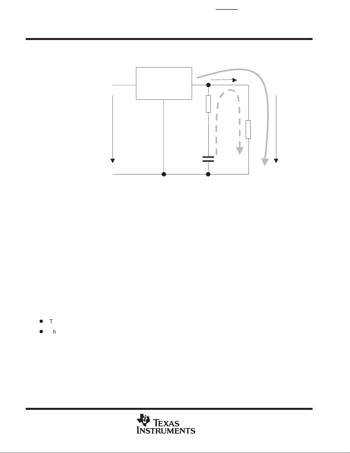
Figure 22 shows the output capacitor and its parasitic impedances in a typical LDO output stage.
I
out
LDO
+
V
ESR
V
in
R
ESR
–
V
R
LOAD
C
out
out
Figure 22. – LDO Output Stage With Parasitic Resistances ESR and ESL
In steady state (dc state condition), the load current is supplied by the LDO (solid arrow) and the voltage across
the capacitor is the same as the output voltage (V
branch. If I
suddenly increases (transient condition), the following occurs;
out
Cout
= V
. This means no current is flowing into the C
out)
out
The LDO is not able to supply the sudden current need due to its response time (t1 in Figure 23). Therefore,
capacitor C
an internal resistance, ESR. Depending on the current demand at the output, a voltage drop will occur at R
This voltage is shown as V
When C
discharge of C
provides the current for the new load condition (dashed arrow). C
out
in Figure 22.
ESR
is conducting current to the load, initial voltage at the load will be V
out
, the output voltage V
out
will drop continuously until the response time t1 of the LDO is reached
out
now acts like a battery with
out
out
= V
Cout
– V
. Due to the
ESR
ESR
and the LDO will resume supplying the load. From this point, the output voltage starts rising again until it reaches
the regulated voltage. This period is shown as t
in Figure 23.
2
The figure also shows the impact of different ESRs on the output voltage. The left brackets show different levels
of ESRs where number 1 displays the lowest and number 3 displays the highest ESR.
From above, the following conclusions can be drawn:
D
The higher the ESR, the larger the droop at the beginning of load transient.
D
The smaller the output capacitor, the faster the discharge time and the bigger the voltage droop during the
LDO response period.
.
18
POST OFFICE BOX 655303 • DALLAS, TEXAS 75265

TPS77301, TPS77318, TPS77327, TPS77328, TPS77333 WITH RESET OUTPUT
TPS77401, TPS77418, TPS77427, TPS77428, TPS77433 WITH POWER GOOD OUTPUT
250-mA LDO REGULATORS WITH INTEGRATED RESET OR PG
SLVS281A – FEBRUARY 2000 – REVISED MARCH 2000
APPLICATION INFORMATION
conclusion
To minimize the transient output droop, capacitors must have a low ESR and be large enough to support the
minimum output voltage requirement.
I
out
V
out
1
2
3
ESR 1
ESR 2
ESR 3
t
1
t
2
Figure 23. – Correlation of Different ESRs and Their Influence to the Regulation of V
Load Step From Low-to-High Output Current
out
at a
POST OFFICE BOX 655303 • DALLAS, TEXAS 75265
19

TPS77301, TPS77318, TPS77327, TPS77328, TPS77333 WITH RESET OUTPUT
TPS77401, TPS77418, TPS77427, TPS77428, TPS77433 WITH POWER GOOD OUTPUT
250-mA LDO REGULATORS WITH INTEGRATED RESET OR PG
SLVS281A – FEBRUARY 2000 – REVISED MARCH 2000
APPLICATION INFORMATION
programming the TPS77x01 adjustable LDO regulator
The output voltage of the TPS77x01 adjustable regulator is programmed using an external resistor divider as
shown in Figure 28. The output voltage is calculated using:
R1
VO+
V
ǒ1
ref
Where:
V
= 1.1834 V typ (the internal reference voltage)
ref
Resistors R1 and R2 should be chosen for approximately 7-µA divider current. Lower value resistors can be
used but offer no inherent advantage and waste more power. Higher values should be avoided as leakage
currents at FB increase the output voltage error. The recommended design procedure is to choose
R2 = 30.1 kΩ to set the divider current at 7 µA and then calculate R1 using:
V
R1
V
+ ǒ
I
0.1 µF
O
*
V
ref
)
R2
1
Ǔ
TPS77x01
IN
RESET
EN
FB/SENSE
GND
Ǔ
R2
PG or
OUT
PG or RESET Output
250 kΩ
R1
R2
C
OUTPUT VOLTAGE
PROGRAMMING GUIDE
OUTPUT
VOLTAGE
2.5 V
V
O
O
3.3 V
3.6 V
NOTE: To reduce noise and prevent
oscillation, R1 and R2 need to be as
close as possible to the FB/SENSE
terminal.
R1 R2
169
174
169
287
169
324
(1)
(2)
UNIT
kΩ
kΩ
kΩ
Figure 24. TPS77x01 Adjustable LDO Regulator Programming
20
POST OFFICE BOX 655303 • DALLAS, TEXAS 75265

TPS77301, TPS77318, TPS77327, TPS77328, TPS77333 WITH RESET OUTPUT
TPS77401, TPS77418, TPS77427, TPS77428, TPS77433 WITH POWER GOOD OUTPUT
250-mA LDO REGULATORS WITH INTEGRATED RESET OR PG
SLVS281A – FEBRUARY 2000 – REVISED MARCH 2000
APPLICATION INFORMATION
regulator protection
The TPS773xx or TPS774xx PMOS-pass transistor has a built-in back diode that conducts reverse currents
when the input voltage drops below the output voltage (e.g., during power down). Current is conducted from
the output to the input and is not internally limited. When extended reverse voltage is anticipated, external
limiting may be appropriate.
The TPS773xx or TPS774xx also features internal current limiting and thermal protection. During normal
operation, the TPS773xx or TPS774xx limits output current to approximately 0.9 A. When current limiting
engages, the output voltage scales back linearly until the overcurrent condition ends. While current limiting is
designed to prevent gross device failure, care should be taken not to exceed the power dissipation ratings of
the package. If the temperature of the device exceeds 150°C(typ), thermal-protection circuitry shuts it down.
Once the device has cooled below 130°C(typ), regulator operation resumes.
power dissipation and junction temperature
Specified regulator operation is assured to a junction temperature of 125°C; the maximum junction temperature
should be restricted to 125°C under normal operating conditions. This restriction limits the power dissipation
the regulator can handle in any given application. T o ensure the junction temperature is within acceptable limits,
calculate the maximum allowable dissipation, P
or equal to P
The maximum-power-dissipation limit is determined using the following equation:
D(max)
.
, and the actual dissipation, PD, which must be less than
D(max)
P
D(max)
Where:
T
max is the maximum allowable junction temperature
J
R
is the thermal resistance junction-to-ambient for the package, i.e., 266.2°C/W for the 8-terminal
θJA
MSOP with no airflow.
T
is the ambient temperature.
A
The regulator dissipation is calculated using:
PD+ǒVI*
Power dissipation resulting from quiescent current is negligible. Excessive power dissipation will trigger the
thermal protection circuit.
TJmax*T
+
R
V
O
Ǔ
A
q
JA
I
O
POST OFFICE BOX 655303 • DALLAS, TEXAS 75265
21

TPS77301, TPS77318, TPS77327, TPS77328, TPS77333 WITH RESET OUTPUT
TPS77401, TPS77418, TPS77427, TPS77428, TPS77433 WITH POWER GOOD OUTPUT
250-mA LDO REGULATORS WITH INTEGRATED RESET OR PG
SLVS281A – FEBRUARY 2000 – REVISED MARCH 2000
MECHANICAL DATA
DGK (R-PDSO-G8) PLASTIC SMALL-OUTLINE PACKAGE
0,65
8
1
1,07 MAX
3,05
2,95
0,38
0,25
5
3,05
2,95
4
Seating Plane
0,15
0,05
0,25
4,98
4,78
M
0,10
0,15 NOM
Gage Plane
0°–6°
0,25
0,69
0,41
NOTES: A. All linear dimensions are in millimeters.
B. This drawing is subject to change without notice.
C. Body dimensions do not include mold flash or protrusion.
D. Falls within JEDEC MO-187
4073329/B 04/98
22
POST OFFICE BOX 655303 • DALLAS, TEXAS 75265

IMPORTANT NOTICE
T exas Instruments and its subsidiaries (TI) reserve the right to make changes to their products or to discontinue
any product or service without notice, and advise customers to obtain the latest version of relevant information
to verify, before placing orders, that information being relied on is current and complete. All products are sold
subject to the terms and conditions of sale supplied at the time of order acknowledgment, including those
pertaining to warranty, patent infringement, and limitation of liability.
TI warrants performance of its semiconductor products to the specifications applicable at the time of sale in
accordance with TI’s standard warranty. Testing and other quality control techniques are utilized to the extent
TI deems necessary to support this warranty . Specific testing of all parameters of each device is not necessarily
performed, except those mandated by government requirements.
Of course, customers are responsible for their applications using TI components.
In order to minimize risks associated with the customer’s applications, adequate design and operating
safeguards must be provided by the customer to minimize inherent or procedural hazards.
TI assumes no liability for applications assistance or customer product design. TI does not warrant or represent
that any license, either express or implied, is granted under any patent right, copyright, mask work right, or other
intellectual property right of TI covering or relating to any combination, machine, or process in which such
semiconductor products or services might be or are used. TI’s publication of information regarding any third
party’s products or services does not constitute TI’s approval, warranty or endorsement thereof.
Copyright 2000, Texas Instruments Incorporated
 Loading...