


Texas Instruments TPS76933DBVR, TPS76930DBVT, TPS76930DBVR, TPS76928DBVT, TPS76928DBVR Datasheet
...
TPS76901, TPS76912, TPS76915, TPS76918, TPS76925
TPS76927, TPS76928, TPS76930, TPS76933, TPS76950
ULTRALOW-POWER 100-mA LOW-DROPOUT LINEAR REGULATORS
SLVS203D – JUNE 1999 – REVISED APRIL 2000
1
POST OFFICE BOX 655303 • DALLAS, TEXAS 75265
D
100-mA Low-Dropout Regulator
D
Available in 1.2-V, 1.5-V, 1.8-V, 2.5-V, 2.7-V,
2.8-V, 3.0-V, 3.3-V, and 5-V Fixed-Output and
Adjustable Versions
D
Only 17 µA Quiescent Current at 100 mA
D
1 µA Quiescent Current in Standby Mode
D
Dropout Voltage Typically 71 mV at 100mA
D
Over Current Limitation
D
–40°C to 125°C Operating Junction
T emperature Range
D
5-Pin SOT-23 (DBV) Package
description
The TPS769xx family of low-dropout (LDO)
voltage regulators offers the benefits of low
dropout voltage, ultralow-power operation, and
miniaturized packaging. These regulators feature
low dropout voltages and ultralow quiescent
current compared to conventional LDO
regulators. Offered in a 5-terminal small outline
integrated-circuit SOT-23 package, the
TPS769xx series devices are ideal for
micropower operations and where board space is
at a premium.
A combination of new circuit design and process
innovation has enabled the usual PNP pass
transistor to be replaced by a PMOS pass
element. Because the PMOS pass element
behaves as a low-value resistor, the dropout
voltage is very low, typically 71 mV at 100 mA of
load current (TPS76950), and is directly proportional to the load current. Since the PMOS pass element is a
voltage-driven device, the quiescent current is ultralow (28 µA maximum) and is stable over the entire range
of output load current (0 mA to 100 mA). Intended for use in portable systems such as laptops and cellular
phones, the ultralow-dropout voltage feature and ultralow-power operation result in a significant increase in
system battery operating life.
The TPS769xx also features a logic-enabled sleep mode to shut down the regulator, reducing quiescent current
to 1 µA typical at T
J
= 25°C. The TPS769xx is offered in 1.2-V, 1.5-V, 1.8-V, 2.5-V, 2.7-V, 2.8-V, 3.0-V, 3.3-V,
and 5-V fixed-voltage versions and in a variable version (programmable over the range of 1.2 V to 5.5 V).
Copyright 2000, Texas Instruments Incorporated
PRODUCTION DATA information is current as of publication date.
Products conform to specifications per the terms of Texas Instruments
standard warranty. Production processing does not necessarily include
testing of all parameters.
Please be aware that an important notice concerning availability, standard warranty, and use in critical applications of
Texas Instruments semiconductor products and disclaimers thereto appears at the end of this data sheet.
3
2
4
5
DBV PACKAGE
(TOP VIEW)
1
IN
GND
EN
OUT
NC/FB
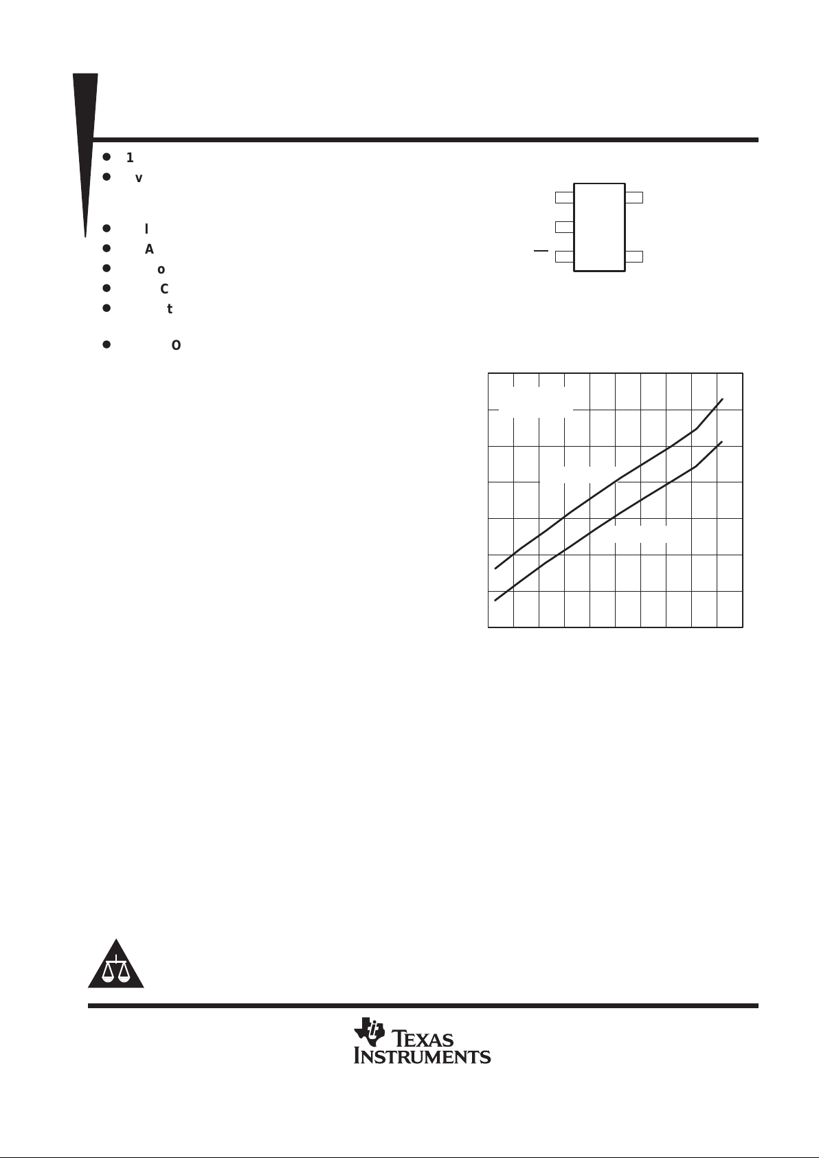
TA – Free-Air Temperature – °C
15
22
TPS76933
GROUND CURRENT
vs
FREE-AIR TEMPERATURE
Ground Current – Aµ
VI = 4.3 V
CO = 4.7 µF
–40 0–20 20 140–60 40 80 100 12060
21
20
19
18
17
16
IO = 0 mA
IO = 100 mA
TPS76901, TPS76912, TPS76915, TPS76918, TPS76925
TPS76927, TPS76928, TPS76930, TPS76933, TPS76950
ULTRALOW-POWER 100-mA LOW-DROPOUT LINEAR REGULATORS
SLVS203D – JUNE 1999 – REVISED APRIL 2000
2
POST OFFICE BOX 655303 • DALLAS, TEXAS 75265
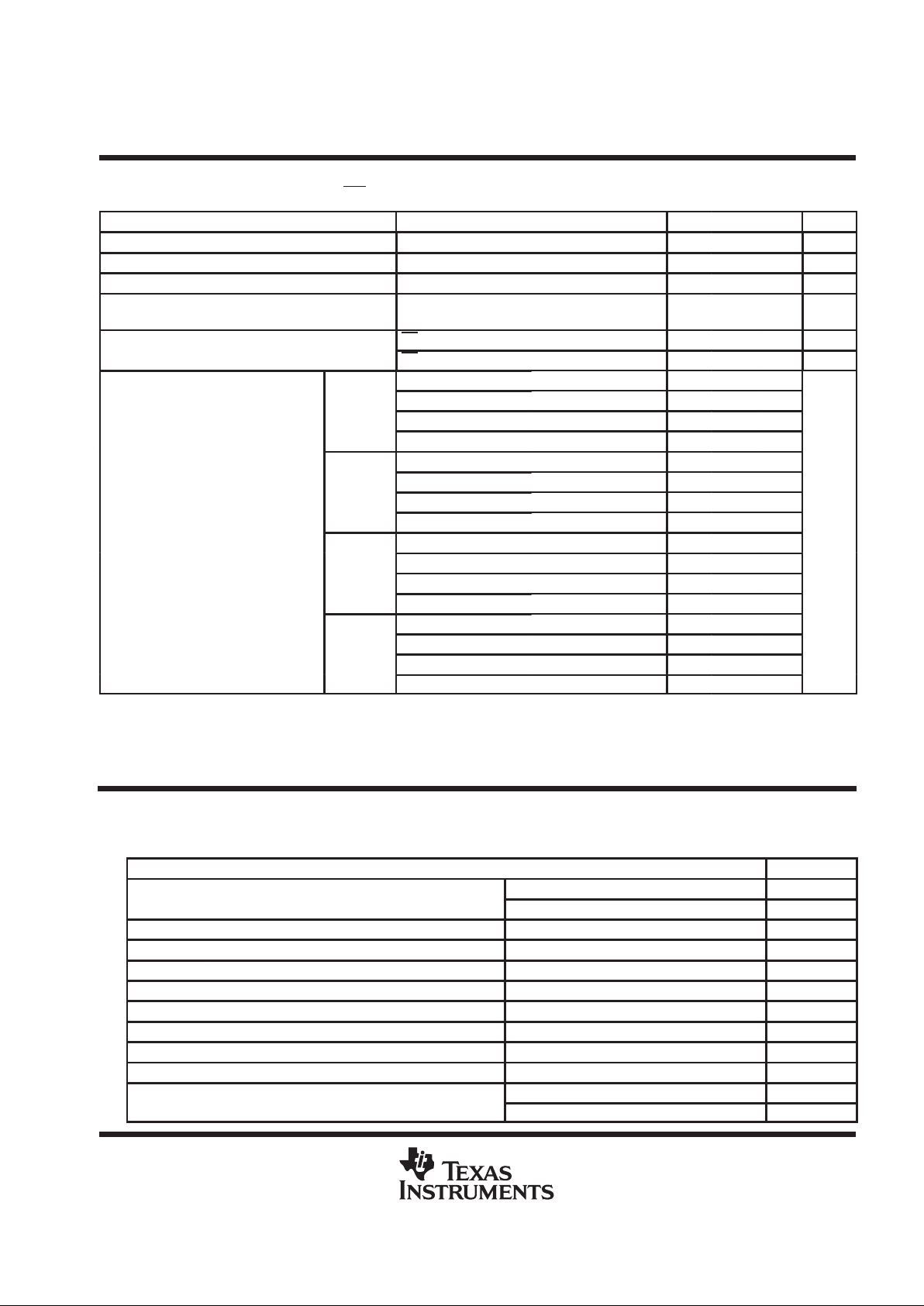
AVAILABLE OPTIONS
T
J
VOLTAGE PACKAGE PART NUMBER SYMBOL
Variable
1.2V to 5.5V
TPS76901DBVT†TPS76901DBVR
‡
PCFI
1.2 V TPS76912DBVT†TPS76912DBVR
‡
PCGI
1.5 V TPS76915DBVT†TPS76915DBVR
‡
PCHI
1.8 V
TPS76918DBVT†TPS76918DBVR
‡
PCII
–40°C to 125°C
2.5 V
SOT-23
TPS76925DBVT†TPS76925DBVR
‡
PCJI
2.7 V
(DBV)
TPS76927DBVT†TPS76927DBVR
‡
PCKI
2.8 V TPS76928DBVT†TPS76928DBVR
‡
PCLI
3.0 V TPS76930DBVT†TPS76930DBVR
‡
PCMI
3.3 V TPS76933DBVT†TPS76933DBVR
‡
PCNI
5.0 V TPS76950DBVT†TPS76950DBVR
‡
PCOI
†
The DBVT indicates tape and reel of 250 parts.
‡
The DBVR indicates tape and reel of 3000 parts.
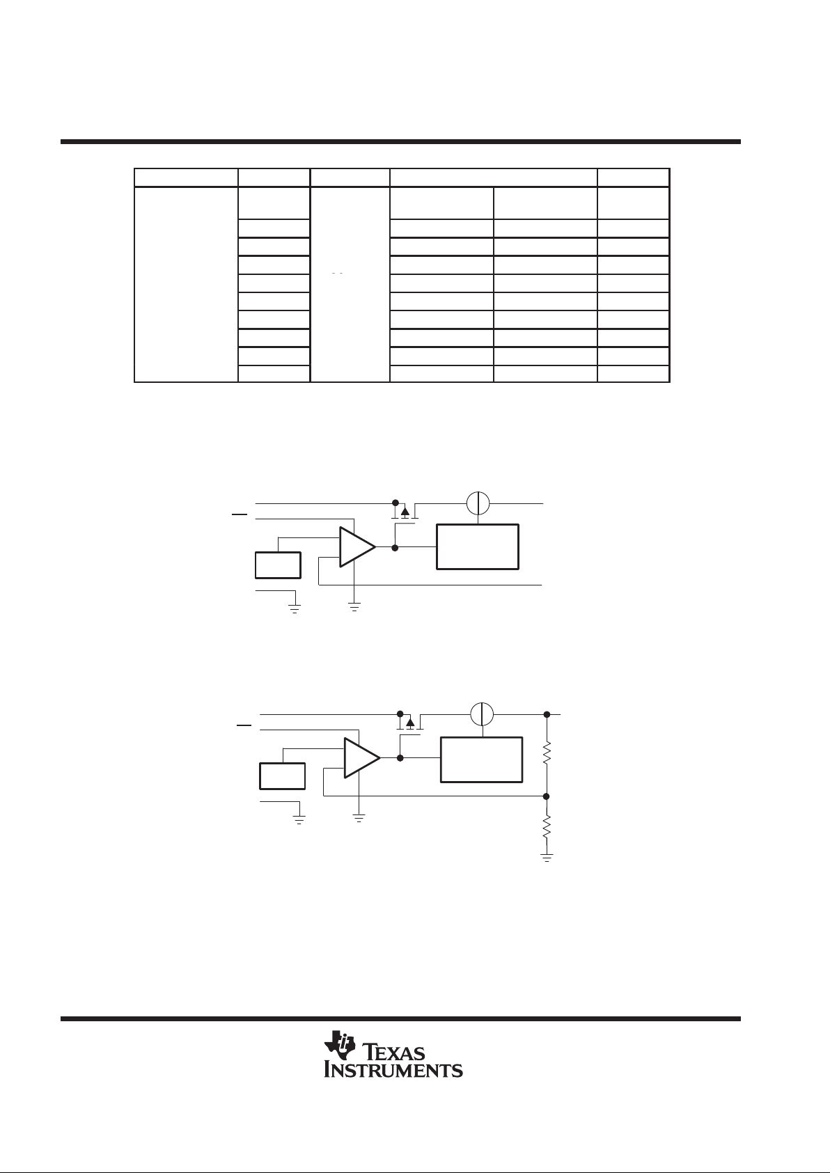
functional block diagram
TPS76901
OUT
IN
FB
GND
EN
V
REF
TPS76912/15/18/25/27/28/30/33/50
OUT
IN
GND
EN
V
REF
Current Limit
/ Thermal
Protection
Current Limit
/ Thermal
Protection
TPS76901, TPS76912, TPS76915, TPS76918, TPS76925
TPS76927, TPS76928, TPS76930, TPS76933, TPS76950
ULTRALOW-POWER 100-mA LOW-DROPOUT LINEAR REGULATORS
SLVS203D – JUNE 1999 – REVISED APRIL 2000
3
POST OFFICE BOX 655303 • DALLAS, TEXAS 75265
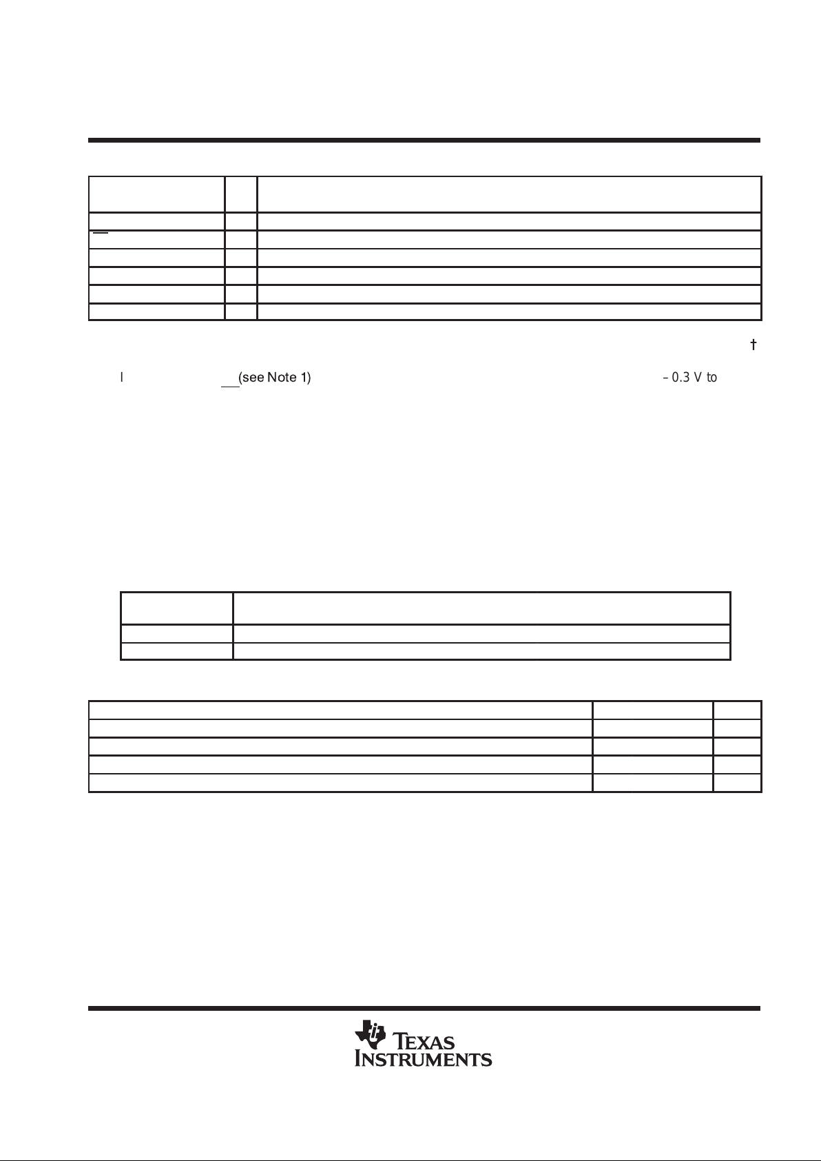
Terminal Functions
TERMINAL
NAME NO.
I/O
DESCRIPTION
GND 2 Ground
EN 3 I Enable input
FB 4 I Feedback voltage (TPS76901 only)
IN 1 I Input supply voltage
NC 4 No connection (Fixed options only)
OUT 5 O Regulated output voltage
absolute maximum ratings over operating free-air temperature range (unless otherwise noted)
Ĕ
Input voltage range
(see Note 1)
–0.3 V to 13.5 V. . . . . . . . . . . . . . . . . . . . . . . . . . . . . . . . . . . . . . . . . . . . . . . . . .
Voltage range at EN –0.3 V to VI + 0.3 V. . . . . . . . . . . . . . . . . . . . . . . . . . . . . . . . . . . . . . . . . . . . . . . . . . . . . . . . . . .
Voltage on OUT, FB 7 V. . . . . . . . . . . . . . . . . . . . . . . . . . . . . . . . . . . . . . . . . . . . . . . . . . . . . . . . . . . . . . . . . . . . . . . . . .
Peak output current Internally limited. . . . . . . . . . . . . . . . . . . . . . . . . . . . . . . . . . . . . . . . . . . . . . . . . . . . . . . . . . . . . .
ESD rating, HBM 2 kV. . . . . . . . . . . . . . . . . . . . . . . . . . . . . . . . . . . . . . . . . . . . . . . . . . . . . . . . . . . . . . . . . . . . . . . . . .
Continuous total power dissipation See Dissipation Rating Table. . . . . . . . . . . . . . . . . . . . . . . . . . . . . . . . . . . . .
Operating virtual junction temperature range, T
J
–40°C to 150°C. . . . . . . . . . . . . . . . . . . . . . . . . . . . . . . . . . . . .
Storage temperature range, T
stg
–65°C to 150°C. . . . . . . . . . . . . . . . . . . . . . . . . . . . . . . . . . . . . . . . . . . . . . . . . . .
†
Stresses beyond those listed under “absolute maximum ratings” may cause permanent damage to the device. These are stress ratings only, and
functional operation of the device at these or any other conditions beyond those indicated under “recommended operating conditions” is not
implied. Exposure to absolute-maximum-rated conditions for extended periods may affect device reliability.
NOTE 1: All voltage values are with respect to network ground terminal.
DISSIPATION RATING TABLE
PACKAGE
TA ≤ 25°C
POWER RATING
DERATING FACTOR
ABOVE TA = 25°C
TA = 70°C
POWER RATING
TA = 85°C
POWER RATING
Recommended DBV 350 mW 3.5 mW/°C 192 mW 140 mW
Absolute Maximum DBV 437 mW 3.5 mW/°C 280 mW 227 mW
recommended operating conditions
MIN NOM MAX UNIT
Input voltage, VI (see Note 2) 2.7 10 V
Output voltage range, V
O
1.2 5.5 V
Continuous output current, IO (see Note 3) 0 100 mA
Operating junction temperature, T
J
–40 125 °C
NOTES: 2. To calculate the minimum input voltage for your maximum output current, use the following formula:
VI(min) = VO(max) + VDO (max load)
3. Continuous output current and operating junction temperature are limited by internal protection circuitry , but it is not recommended
that the device operate under conditions beyond those specified in this table for extended periods of time.
TPS76901, TPS76912, TPS76915, TPS76918, TPS76925
TPS76927, TPS76928, TPS76930, TPS76933, TPS76950
ULTRALOW-POWER 100-mA LOW-DROPOUT LINEAR REGULATORS
SLVS203D – JUNE 1999 – REVISED APRIL 2000
4
POST OFFICE BOX 655303 • DALLAS, TEXAS 75265
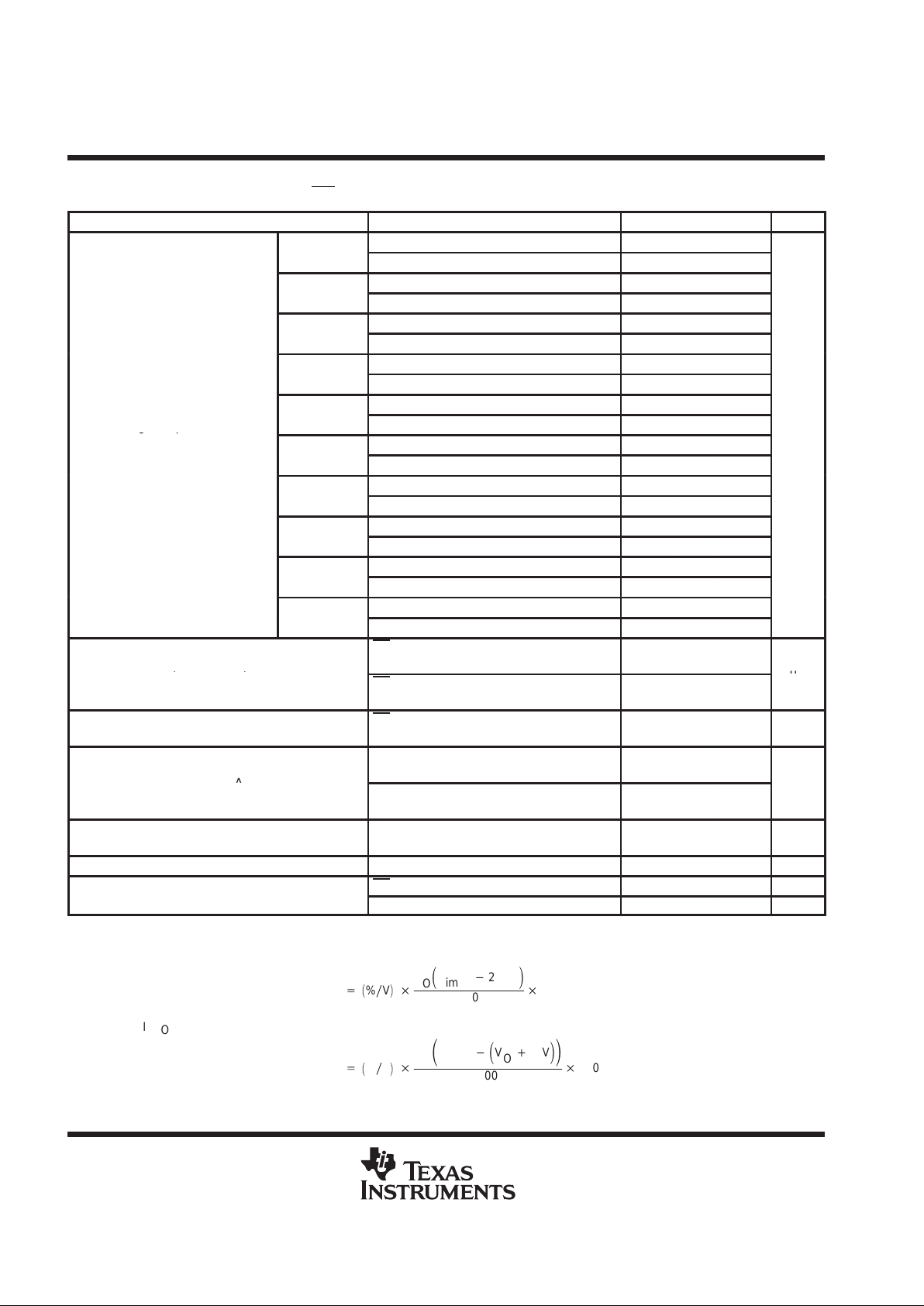
electrical characteristics over recommended operating free-air temperature range,
V
I
= V
O(typ)
+ 1 V, I
O
= 100 mA, EN = 0 V, C
O
= 4.7 µF (unless otherwise noted)
PARAMETER TEST CONDITIONS MIN TYP MAX UNIT
1.2 V ≤ VO ≤ 5.5 V, TJ = 25°C V
O
TPS76901
1.2 V ≤ VO ≤ 5.5 V, TJ = –40°C to 125°C 0.97V
O
1.03V
O
TJ = 25°C, 2.7 V < VIN < 10 V 1.224
TPS76912
TJ = –40°C to 125°C, 2.7 V < VIN < 10 V 1.187 1.261
TJ = 25°C, 2.7 V < VIN < 10 V 1.5
TPS76915
TJ = –40°C to 125°C, 2.7 V < VIN < 10 V 1.455 1.545
TJ = 25°C, 2.8 V < VIN < 10 V 1.8
TPS76918
TJ = –40°C to 125°C, 2.8 V < VIN < 10 V 1.746 1.854
TJ = 25°C, 3.5 V < VIN < 10 V 2.5
Output voltage (10 µA to 100 mA
TPS76925
TJ = –40°C to 125°C, 3.5 V < VIN < 10 V 2.425 2.575
g( µ
load) (see Note 4)
TJ = 25°C, 3.7 V < VIN < 10 V 2.7
V
TPS76927
TJ = –40°C to 125°C, 3.7 V < VIN < 10 V 2.619 2.781
TJ = 25°C, 3.8 V < VIN < 10 V 2.8
TPS76928
TJ = –40°C to 125°C, 3.8 V < VIN < 10 V 2.716 2.884
TJ = 25°C, 4.0 V < VIN < 10 V 3.0
TPS76930
TJ = –40°C to 125°C, 4.0 V < VIN < 10 V 2.910 3.090
TJ = 25°C, 4.3 V < VIN < 10 V 3.3
TPS76933
TJ = –40°C to 125°C, 4.3 V < VIN < 10 V 3.201 3.399
TJ = 25°C, 6.0 V < VIN < 10 V 5.0
TPS76950
TJ = –40°C to 125°C, 6.0 V < VIN < 10 V 4.850 5.150
Quiescent current (GND current)
EN = 0V, 0 mA < IO < 100 mA,
TJ = 25°C
17
()
(See Note 4 and Note 5)
EN = 0V, IO = 100 mA,
TJ = –40°C to 125°C
28
µ
A
Load regulation
EN = 0V, IO = 0 to 100 mA,
TJ = 25°C
12 mV
p
VO + 1 V < VI ≤ 10 V, TJ = 25°C,
See Note 4
0.04
Output voltage line regulation (∆VO/VO) (See Note 5)
VO + 1 V < VI ≤ 10 V,
TJ = –40°C to 125°C, See Note 4
0.1
%/V
Output noise voltage
BW = 300 Hz to 50 kHz,
CO = 10 µF, TJ = 25°C
190 µVrms
Output current limit VO = 0 V, See Note 4 350 750 mA
EN = VI, 2.7 < VI < 10 V 1 µA
Standby current
TJ = –40°C to 125°C 2 µA
NOTES: 4. Minimum IN operating voltage is 2.7 V or V
O(typ)
+ 1 V , whichever is greater. Maximum IN voltage 10 V, minimum output current
10 µA, maximum output current 100 mA.
5. If VO≤ 1.8 V then V
imin
= 2.7 V, V
imax
= 10 V:
Line Reg. (mV)
+ǒ%ńVǓ
V
O
ǒ
V
imax
*
2.7 V
Ǔ
100
1000
If VO ≥ 2.5 V then V
imin
= VO + 1 V, V
imax
= 10 V:
Line Reg. (mV)
+ǒ%ńVǓ
V
O
ǒ
V
imax
*ǒVO)
1V
Ǔ
Ǔ
100
1000
TPS76901, TPS76912, TPS76915, TPS76918, TPS76925
TPS76927, TPS76928, TPS76930, TPS76933, TPS76950
ULTRALOW-POWER 100-mA LOW-DROPOUT LINEAR REGULATORS
SLVS203D – JUNE 1999 – REVISED APRIL 2000
5
POST OFFICE BOX 655303 • DALLAS, TEXAS 75265
electrical characteristics over recommended operating free-air temperature range,
V
I
= V
O(typ)
+ 1 V, I
O
= 100 mA, EN = 0 V, C
O
= 4.7 µF (unless otherwise noted) (continued)
PARAMETER TEST CONDITIONS
MIN TYP MAX UNIT
FB input current FB = 1.224 V (TPS76901) –1 1 µA
High level enable input voltage 2.7 V < VI < 10 V 1.7 V
Low level enable input voltage 2.7 V < VI < 10 V 0.9 V
Power supply ripple rejection
f = 1 kHz, CO = 10 µF,
TJ = 25°C, See Note 4
60 dB
p
EN = 0 V –1 0 1 µA
Input current (EN)
EN = V
I
–1 1 µA
IO = 50 mA, TJ = 25°C 60
IO = 50 mA, TJ = –40°C to 125°C 125
TPS76928
IO = 100 mA, TJ = 25°C 122
IO = 100 mA, TJ = –40°C to 125°C 245
IO = 50 mA, TJ = 25°C 57
IO = 50 mA, TJ = –40°C to 125°C 115
TPS76930
IO = 100 mA, TJ = 25°C 115
p
IO = 100 mA, TJ = –40°C to 125°C 230
Dropout voltage (See Note 6)
IO = 50 mA, TJ = 25°C 48
mV
IO = 50 mA, TJ = –40°C to 125°C 100
TPS76933
IO = 100 mA, TJ = 25°C 98
IO = 100 mA, TJ = –40°C to 125°C 200
IO = 50 mA, TJ = 25°C 35
IO = 50 mA, TJ = –40°C to 125°C 85
TPS76950
IO = 100 mA, TJ = 25°C 71
IO = 100 mA, TJ = –40°C to 125°C 170
NOTES: 4. Minimum IN operating voltage is 2.7 V or V
O(typ)
+ 1 V , whichever is greater. Maximum IN voltage 10 V, minimum output current
10 µA, maximum output current 100 mA.
6. IN voltage equals VO(Typ) – 100mV; TPS76901 output voltage set to 3.3V nominal with external resistor divider. TPS76912,
TPS76915, TPS76918, TPS76925, and TPS76927 dropout voltage limited by input voltage range limitations.
TYPICAL CHARACTERISTICS
Table of Graphs
FIGURE
p
vs Output current 1, 2, 3
VOOutput voltage
vs Free-air temperature 4, 5, 6
Ground current vs Free-air temperature 7
Output spectral noise density vs Frequency 8
Z
o
Output impedance vs Frequency 9
V
DO
Dropout voltage vs Free-air temperature 10
Ripple rejection vs Frequency 11
LDO startup time 12
Line transient response 13, 15
Load transient response 14, 16
vs Output current 17, 19
Equivalent series resistance (ESR)
vs Added ceramic capacitance 18, 20