

Texas Instruments TPS76150DBVT, TPS76150DBVR, TPS76138DBVT, TPS76133DBVT, TPS76138DBVR Datasheet
...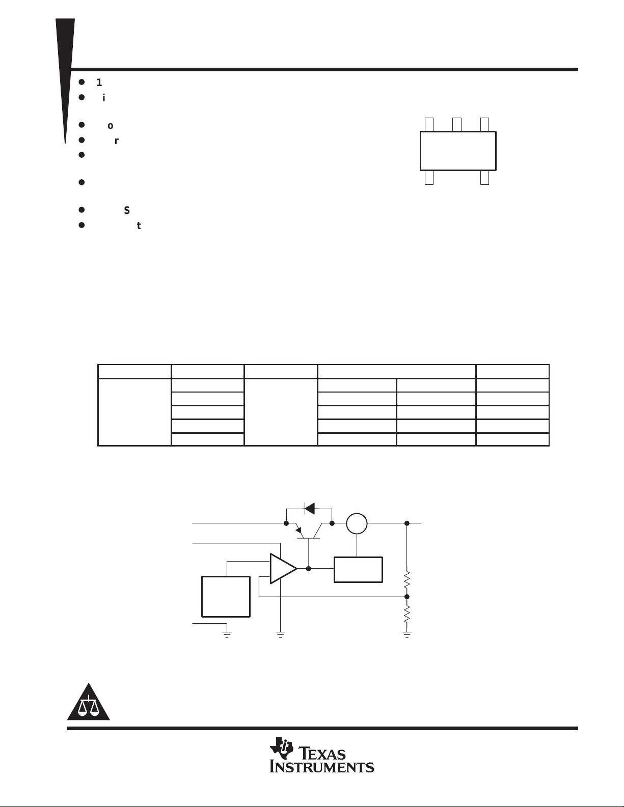
(DBV)
TPS76130, TPS76132, TPS76133, TPS76138, TPS76150
LOW-POWER 100-mA LOW-DROPOUT LINEAR REGULATORS
SLVS178A – DECEMBER 1998 – REVISED FEBRUAR Y 1999
D
100-mA Low-Dropout Regulator
D
Fixed Output Voltage Options: 5 V, 3.8 V,
3.3 V, 3.2 V, and 3 V
D
Dropout T ypically 170 mV at 100-mA
D
Thermal Protection
D
Less Than 1 µA Quiescent Current in
Shutdown
D
–40°C to 125°C Operating Junction
T emperature Range
D
5-Pin SOT-23 (DBV) Package
D
ESD Protection Verified to 1.5 KV Human
Body Model (HBM) per MIL-STD-883C
DBV PACKAGE
(TOP VIEW)
EN GND IN
321
45
OUTNC
NC – No internal connection
description
The TPS761xx is a 100 mA, low dropout (LDO) voltage regulator designed specifically for battery-powered
applications. A proprietary BiCMOS fabrication process allows the TPS761xx to provide outstanding
performance in all specifications critical to battery-powered operation.
The TPS761xx is available in a space-saving SOT-23 (DBV) package and operates over a junction temperature
range of –40°C to 125°C.
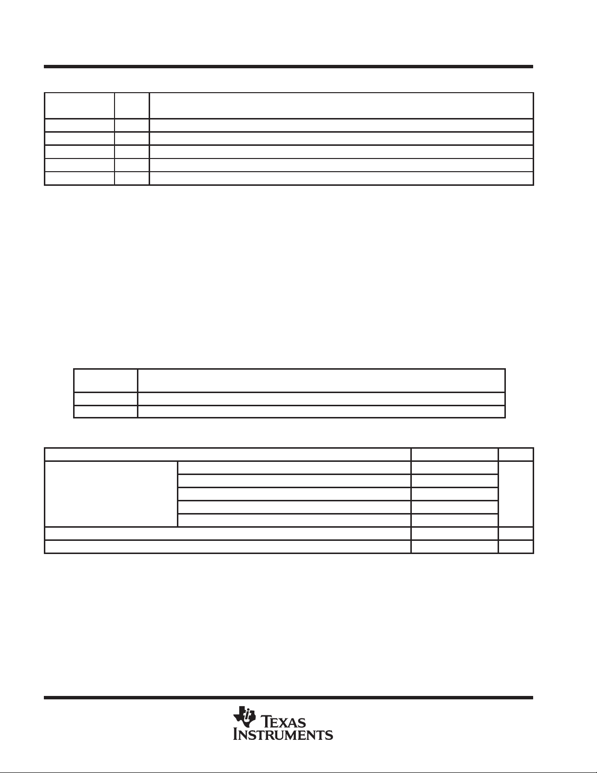
AVAILABLE OPTIONS
T
J
–40°C to 125°C
†
The DBVR passive indicates tape and reel of 3000 parts.
‡
The DBVT passive indicates tape and reel of 250 parts.
VOLTAGE PACKAGE PART NUMBER SYMBOL
3 V TPS76130DBVR†TPS76130DBVT
3.2 V
3.3 V
3.8 V
5 V TPS76150DBVR†TPS76150DBVT
SOT-23
TPS76132DBVR†TPS76132DBVT
TPS76133DBVR†TPS76133DBVT
TPS76138DBVR†TPS76138DBVT
‡
‡
‡
‡
‡
PAEI
PAFI
PAII
PAKI
PALI
functional block diagram
IN
EN
V
ref
Thermal
Sense
GND
§
Current sense
Please be aware that an important notice concerning availability, standard warranty, and use in critical applications of
Texas Instruments semiconductor products and disclaimers thereto appears at the end of this data sheet.
PRODUCTION DATA information is current as of publication date.
Products conform to specifications per the terms of Texas Instruments
standard warranty. Production processing does not necessarily include
testing of all parameters.
CS
Current
Limit
+
POST OFFICE BOX 655303 • DALLAS, TEXAS 75265
§
OUT
Copyright 1999, Texas Instruments Incorporated
1
TPS76130, TPS76132, TPS76133, TPS76138, TPS76150
I/O
DESCRIPTION
LOW-POWER 100-mA LOW-DROPOUT LINEAR REGULATORS
SLVS178A – DECEMBER 1998 – REVISED FEBRUAR Y 1999
Terminal Functions
TERMINAL
NAME NO.
EN 3 I Enable input
GND 2 Ground
IN 1 I Input voltage
NC 4 No connection
OUT 5 O Regulated output voltage
absolute maximum ratings over operating free-air temperature range (unless otherwise noted)
Input voltage range, V
Voltage range at EN –0.3 V to V
Peak output current internally limited. . . . . . . . . . . . . . . . . . . . . . . . . . . . . . . . . . . . . . . . . . . . . . . . . . . . . . . . . . . . . . .
Continuous total dissipation See Dissipation Rating Table. . . . . . . . . . . . . . . . . . . . . . . . . . . . . . . . . . . . . . . . . . . .
Operating junction temperature range, T
Storage temperature range, T
ESD rating, HBM 1.5 kV. . . . . . . . . . . . . . . . . . . . . . . . . . . . . . . . . . . . . . . . . . . . . . . . . . . . . . . . . . . . . . . . . . . . . . . . .
†
Stresses beyond those listed under “absolute maximum ratings” may cause permanent damage to the device. These are stress ratings only, and
functional operation of the device at these or any other conditions beyond those indicated under “recommended operating conditions” is not
implied. Exposure to absolute-maximum-rated conditions for extended periods may affect device reliability.
NOTE 1: All voltages are with respect to device GND pin.
Recommended DBV 350 mW 3.5 mW/°C 192 mW 140 mW
Maximum DBV 437 mW 3.5 mW/° C 280 mW 227 mW
(see Note 1) –0.3 V to 16 V. . . . . . . . . . . . . . . . . . . . . . . . . . . . . . . . . . . . . . . . . . . . . . . . . . . . . . .
I
–40°C to 150°C. . . . . . . . . . . . . . . . . . . . . . . . . . . . . . . . . . . . . . . . . . .
J
stg
DISSIPATION RATING TABLE
PACKAGE
TA ≤ 25°C
POWER RATING
DERATING FACTOR
ABOVE TA = 25°C
TA = 70°C
POWER RATING
–65°C to 150°C. . . . . . . . . . . . . . . . . . . . . . . . . . . . . . . . . . . . . . . . . . . . . . . . . . . . . . . . .
TA = 85°C
POWER RATING
+ 0.3 V. . . . . . . . . . . . . . . . . . . . . . . . . . . . . . . . . . . . . . . . . . . . . . . . . . . . . . . . . . . . . . . . .
I
recommended operating conditions
MIN NOM MAX UNIT
TPS76130 3.35 16
TPS76132 3.58 16
Input voltage, V
Continuous output current, I
Operating junction temperature, T
I
O
TPS76133 3.68 16
TPS76138 4.18 16
TPS76150 5.38 16
0 100 mA
J
–40 125 °C
V
†
2
POST OFFICE BOX 655303 • DALLAS, TEXAS 75265
Quiescent current (GND current)
A
TPS76130, TPS76132, TPS76133, TPS76138, TPS76150
LOW-POWER 100-mA LOW-DROPOUT LINEAR REGULATORS
SLVS178A – DECEMBER 1998 – REVISED FEBRUAR Y 1999
electrical characteristics over recommended operating free-air temperature range,
V
= V
I
V
O
I
I(standby)
V
n
+ 1 V, IO = 1 mA, EN = VI, Co = 4.7 µF (unless otherwise noted)
O(typ)
PARAMETER TEST CONDITIONS MIN TYP MAX UNIT
TJ = 25°C 2.96 3 3.04
TPS76130
TPS76132
Output voltage TPS76133
TPS76138
TPS76150
Standby current EN = 0 V 1 µA
TPS76130 4 V < VI < 16, IO = 1 mA 3 10
TPS76132 4.2 V < VI < 16, IO = 1 mA 3 10
Input regulation
Output noise voltage BW = 300 Hz to 50 kHz Co = 10 µF, TJ = 25°C 190 µVrms
Ripple rejection f = 1 kHz, Co = 10 µF, TJ = 25°C 63 dB
TPS76133
TPS76138 4.8 V < VI < 16, IO = 1 mA 3 10
TPS76150 6 V < VI < 16 IO = 1 mA 3 10
TJ = 25°C, 1 mA < IO < 100 mA 2.9 3.04
1 mA < IO < 100 mA 2.89 3.07
TJ = 25°C 3.16 3.2 3.24
TJ = 25°C, 1 mA < IO < 100 mA 3.11 3.24
1 mA < IO < 100 mA 3.08 3.3
TJ = 25°C 3.26 3.3 3.34
TJ = 25°C, 1 mA < IO < 100 mA 3.21 3.34
1 mA < IO < 100 mA 3.18 3.4
TJ = 25°C 3.76 3.8 3.84
TJ = 25°C, 1 mA < IO < 100 mA 3.71 3.84
1 mA < IO < 100 mA 3.68 3.9
TJ = 25°C 4.95 5 5.05
TJ = 25°C, 1 mA < IO < 100 mA 4.88 5.05
1 mA < IO < 100 mA 4.86 5.1
IO = 0 mA, TJ = 25°C 90 115
IO = 0 mA 130
IO = 1 mA, TJ = 25°C 100 130
IO = 1 mA 170
IO = 10 mA, TJ = 25°C 190 220
IO = 10 mA 260
IO = 50 mA, TJ = 25°C 850 1100
IO = 50 mA 1200
IO = 100 mA, TJ = 25°C 2600 3600
IO = 100 mA 4000
4.3 V < VI < 16, IO = 1 mA 3 10
V
V
V
V
V
µ
mV
POST OFFICE BOX 655303 • DALLAS, TEXAS 75265
3
TPS76130, TPS76132, TPS76133, TPS76138, TPS76150
Dropout voltage
mV
IIInput current (EN)
A
VOOutput voltage
LOW-POWER 100-mA LOW-DROPOUT LINEAR REGULATORS
SLVS178A – DECEMBER 1998 – REVISED FEBRUAR Y 1999
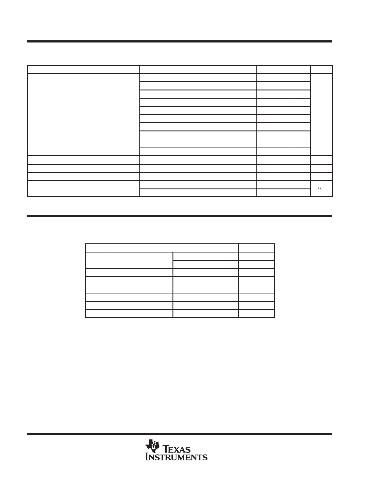
electrical characteristics over recommended operating free-air temperature range,
V
= V
I
+ 1 V, IO = 1 mA, EN = VI, Co = 4.7 µF (unless otherwise noted) (continued)
O(typ)
PARAMETER TEST CONDITIONS MIN TYP MAX UNIT
IO = 0 mA, TJ = 25°C 1 3
IO = 0 mA 5
IO = 1 mA, TJ = 25°C 7 10
IO = 1 mA 15
p
Peak output current/current limit TJ = 25°C 100 150 mA
High level enable input 2 V
Low level enable input 0.8 V
p
IO = 10 mA, TJ = 25°C 40 60
IO = 10 mA 90
IO = 50 mA, TJ = 25°C 120 150
IO = 50 mA 180
IO = 100 mA, TJ = 25°C 170 240
IO = 100 mA 280
EN = 0 V –1 0 1
EN = V
I
2.5 5
µ
TYPICAL CHARACTERISTICS
Table of Graphs
FIGURE
p
Ground current vs Free-air temperature 7, 8, 9
Output noise vs Frequency 10
Z
o
V
DO
Output impedance vs Frequency 11
Dropout voltage vs Free-air temperature 12
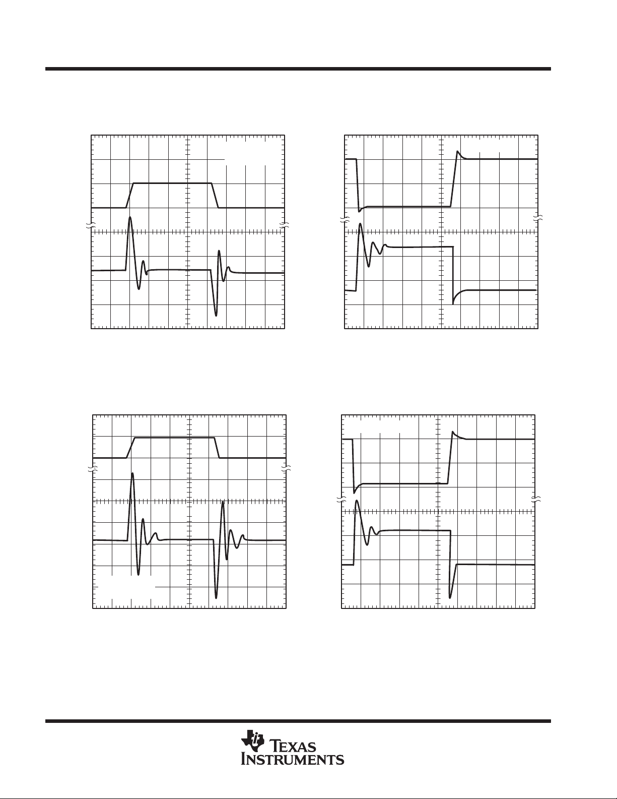
Line transient response 13, 15
Load transient response 14, 16
vs Output current 1, 2, 3
vs Free-air temperature 4, 5, 6
4
POST OFFICE BOX 655303 • DALLAS, TEXAS 75265

TPS76130, TPS76132, TPS76133, TPS76138, TPS76150
LOW-POWER 100-mA LOW-DROPOUT LINEAR REGULATORS
SLVS178A – DECEMBER 1998 – REVISED FEBRUAR Y 1999
TYPICAL CHARACTERISTICS
3.02
3.01
3
2.99
2.98
2.97
– Output Voltage – V
O
V
2.96
2.95
2.94
TPS76130
OUTPUT VOLTAGE
vs
OUTPUT CURRENT
VI = 4 V
CI = CO = 4.7 µF
TA = 25°C
20 60
0 100
40 80 120
IO – Output Current – mA
Figure 1
TPS76133
OUTPUT VOLTAGE
vs
OUTPUT CURRENT
3.32
3.31
3.3
3.29
3.28
3.27
– Output Voltage – V
O
V
3.26
3.25
3.24
20 60
0 100
40 80 120
IO – Output Current – mA
Figure 2
VI = 4.3 V
CI = CO = 4.7 µF
TA = 25°C
5.03
5.02
5.01
5
4.99
4.98
– Output Voltage – V
O
V
4.97
4.96
4.95
TPS76150
OUTPUT VOLTAGE
vs
OUTPUT CURRENT
VI = 6 V
CI = CO = 4.7 µF
TA = 25°C
20 60
0 100
40 80 120
IO – Output Current – mA
Figure 3
3.02
3.01
3
2.99
2.98
2.97
2.96
2.95
– Output Voltage – V
O
2.94
V
2.93
2.92
2.91
–60
TPS76130
OUTPUT VOLTAGE
FREE-AIR TEMPERATURE
IL = 100 mA
VI = 4 V
CI = CO = 4.7 µF
–40
–20 20
0 40 140
TA – Free-Air Temperature – ° C
Figure 4
vs
IL = 1 mA
60 80
100 120
POST OFFICE BOX 655303 • DALLAS, TEXAS 75265
5

TPS76130, TPS76132, TPS76133, TPS76138, TPS76150
LOW-POWER 100-mA LOW-DROPOUT LINEAR REGULATORS
SLVS178A – DECEMBER 1998 – REVISED FEBRUAR Y 1999
TYPICAL CHARACTERISTICS
3.32
3.31
3.3
3.29
3.28
3.27
3.26
3.25
– Output Voltage – V
O
3.24
V
3.23
3.22
3.21
–60
TPS76133
OUTPUT VOLTAGE
FREE-AIR TEMPERATURE
IL = 1 mA
VI = 4.3 V
CI = CO = 4.7 µF
–40
–20 20
0 40 140
TA – Free-Air Temperature – ° C
Figure 5
vs
IL = 100 mA
60 80
100 120
5.02
5
4.98
4.96
4.94
– Output Voltage – V
O
V
4.92
4.9
–60
TPS76150
OUTPUT VOLTAGE
vs
FREE-AIR TEMPERATURE
IL = 1 mA
IL = 100 mA
VI = 6 V
CI = CO = 4.7 µF
–40 0
–20 20 140
TA – Free-Air Temperature – ° C
40 60
80 100
Figure 6
120
TPS76130
GROUND CURRENT
vs
FREE-AIR TEMPERATURE
4
10
VI = 4 V
CI = CO = 4.7 µF
3
10
2
10
Ground Current – Aµ
1
10
–40 0–20 20 140
–60
TA – Free-Air Temperature – ° C
40 60
IL = 100 mA
IL = 50 mA
IL = 1 mA
80 100
120
4
10
VI = 4.3 V
CI = CO = 4.7 µF
3
10
2
10
Ground Current – Aµ
1
10
–40 0–20 20 140
–60
FREE-AIR TEMPERATURE
TA – Free-Air Temperature – ° C
Figure 7
TPS76133
GROUND CURRENT
vs
IL = 100 mA
IL = 1 mA
40 60
80 100
Figure 8
IL = 50 mA
120
6
POST OFFICE BOX 655303 • DALLAS, TEXAS 75265

TPS76130, TPS76132, TPS76133, TPS76138, TPS76150
LOW-POWER 100-mA LOW-DROPOUT LINEAR REGULATORS
SLVS178A – DECEMBER 1998 – REVISED FEBRUAR Y 1999
TYPICAL CHARACTERISTICS
TPS76150
GROUND CURRENT
vs
FREE-AIR TEMPERATURE
4
10
VI = 6 V
CI = CO = 4.7 µF
IL = 100 mA
3
10
2
10
Ground Current – Aµ
1
10
–40 0–20 20 140
–60
TA – Free-Air Temperature – ° C
40 60
IL = 50 mA
IL = 1 mA
80 100
120
–5
10
V/ Hz– Output Voltage Noise – V
–6
10
–7
10
n
–8
10
2
10
Figure 9
OUTPUT NOISE
vs
FREQUENCY
CL = 2.2 µF
IL = 100 mA
CL = 2.2 µF
IL = 1 mA
CL = 10 µF
IL = 100 mA
CL = 10 µF
IL = 1 mA
3
10
f – Frequency – Hz
Figure 10
10
4
10
5
OUTPUT IMPEDANCE
vs
FREQUENCY
3
10
CL = 2.2 µF
IL = 50 mA
2
10
Ω
1
10
0
10
– Output Impedance –Z
o
–1
10
–2
10
1
10
10
CL = 2.2 µF
IL = 1 mA
CL = 10 µF
IL = 1 mA
CL = 10 µF
IL = 100 mA
2
3
10
f – Frequency – Hz
CL = 2.2 µF
IL = 100 mA
CL = 10 µF
IL = 50 mA
4
10
10
10
6
5
300
250
200
150
100
– Dropout Voltage – mV
DO
V
50
0
–60 40 60
FREE-AIR TEMPERATURE
VI = EN = 2.9 V
CI = CO = 4.7 µF
IL = 0 mA
–20 20 140
–40 0
TA – Free-Air Temperature – ° C
Figure 11
TPS76130
DROPOUT VOLTAGE
vs
IL = 100 mA
IL = 50 mA
IL = 1 mA
Figure 12
80 100
120
POST OFFICE BOX 655303 • DALLAS, TEXAS 75265
7
TPS76130, TPS76132, TPS76133, TPS76138, TPS76150
LOW-POWER 100-mA LOW-DROPOUT LINEAR REGULATORS
SLVS178A – DECEMBER 1998 – REVISED FEBRUAR Y 1999
TYPICAL CHARACTERISTICS
TPS76130
LINE TRANSIENT RESPONSE
7
6
5
4
– Input Voltage – V
I
V
20
10
0
– Change in
O
–10
V
∆
Output Voltage – mV
–20
–50 15010050 200 250 350300 400 450
0
t – Time – µs
CO = 4.7 µF
IL = 100 mA
Figure 13
TPS76150
LINE TRANSIENT RESPONSE
8
7
TPS76130
LOAD TRANSIENT RESPONSE
40
30
20
10
O
I – Output Current – mA
100
50
0
– Change in∆
O
–50
V
Output Voltage – mV
–100
–300 0–100–200 100 200 400300 500 600 700
t – Time – µs
CO = 4.7 µF
Figure 14
TPS76150
LOAD TRANSIENT RESPONSE
30
CO = 4.7 µF
20
6
30
– Input Voltage – V
I
V
20
10
0
–10
– Change in
O
V
∆
Output Voltage – mV
CO = 4.7 µF
–20
IL = 100 mA
–30
–50 100500 150 200 300250 350 400 450
t – Time – µs
Figure 15
10
0
O
I – Output Current – mA
100
50
0
– Change in∆
O
–50
V
Output Voltage – mV
–100
–300 0–100–200 100 200 400300 500 600 700
t – Time – µs
Figure 16
8
POST OFFICE BOX 655303 • DALLAS, TEXAS 75265

TPS76130, TPS76132, TPS76133, TPS76138, TPS76150
LOW-POWER 100-mA LOW-DROPOUT LINEAR REGULATORS
SLVS178A – DECEMBER 1998 – REVISED FEBRUAR Y 1999
APPLICATION INFORMATION
IN
CI = 1 µF
EN
1
TPS761xx
3
2
GND
5
OUT
Co = 4.7 µF
Figure 17. TPS761xx Typical Application
over current protection
The over current protection circuit forces the TPS761xx into a constant current output mode when the load is
excessive or the output is shorted to ground. Normal operation resumes when the fault condition is removed.
NOTE:
An overload or short circuit may also activate the over temperature protection if the fault
condition persists.
over temperature protection
The thermal protection system shuts the TPS761xx down when the junction temperature exceeds 160°C. The
device recovers and operates normally when the temperature drops below 150°C.
input capacitor
A 1-µF or larger ceramic decoupling capacitor with short leads connected between IN and GND is
recommended. The decoupling capacitor may be omitted if there is a 1 µF or larger electrolytic capacitor
connected between IN and GND and located reasonably close to the TPS761xx. However, the small ceramic
device is desirable even when the larger capacitor is present, if there is a lot of high frequency noise present
in the system.
output capacitor
Like all low dropout regulators, the TPS761xx requires an output capacitor connected between OUT and GND
to stabilize the internal control loop. The minimum recommended capacitance value is 4.7 µF and the ESR
(equivalent series resistance) must be between 0.1 Ω and 10 Ω. Solid tantalum electrolytic, aluminum
electrolytic, and multilayer ceramic capacitors are all suitable, provided they meet the requirements described
above. Most of the commercially available 4.7-µF surface-mount solid-tantalum capacitors, including devices
from Sprague, Kemet, and Nichicon, meet the ESR requirements stated above. Multilayer ceramic capacitors
should have minimum values of 4.7 µF over the full operating temperature range of the equipment.
enable (EN)
A logic zero on the enable input shuts the TPS761xx off and reduces the supply current to less than 1 µA. Pulling
the enable input high causes normal operation to resume. If the enable feature is not used, EN should be
connected to IN to keep the regulator on all of the time. The EN input must not be left floating.
reverse current path
The power transistor used in the TPS761xx has an inherent diode connected between IN and OUT as shown
in the functional block diagram. This diode conducts current from the OUT terminal to the IN terminal whenever
IN is lower than OUT by a diode drop. This condition does not damage the TPS761xx provided the current is
limited to 150 mA.
POST OFFICE BOX 655303 • DALLAS, TEXAS 75265
9
TPS76130, TPS76132, TPS76133, TPS76138, TPS76150
LOW-POWER 100-mA LOW-DROPOUT LINEAR REGULATORS
SLVS178A – DECEMBER 1998 – REVISED FEBRUAR Y 1999
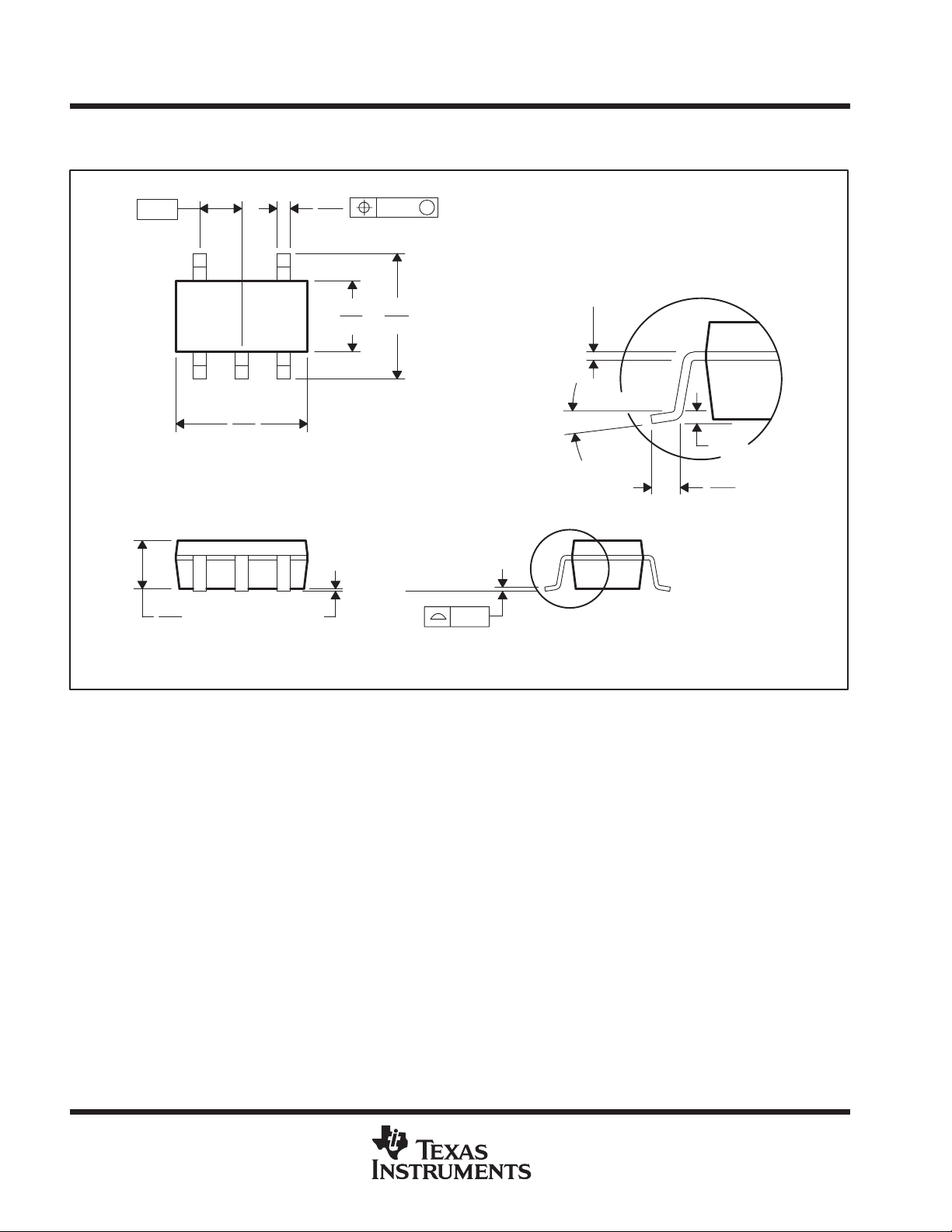
MECHANICAL DATA
DBV (R-PDSO-G5) PLASTIC SMALL-OUTLINE PACKAGE
0,95
1,30
1,00
0,40
0,20
45
1,80
1,50
1
3,10
2,70
3
0,05 MIN
M
0,25
3,00
2,50
Seating Plane
0,10
0,15 NOM
0°–8°
Gage Plane
0,25
0,55
0,35
NOTES: A. All linear dimensions are in millimeters.
B. This drawing is subject to change without notice.
C. Body dimensions include mold flash or protrusion.
Aug/18/1998
10
POST OFFICE BOX 655303 • DALLAS, TEXAS 75265

IMPORTANT NOTICE
T exas Instruments and its subsidiaries (TI) reserve the right to make changes to their products or to discontinue
any product or service without notice, and advise customers to obtain the latest version of relevant information
to verify, before placing orders, that information being relied on is current and complete. All products are sold
subject to the terms and conditions of sale supplied at the time of order acknowledgement, including those
pertaining to warranty, patent infringement, and limitation of liability.
TI warrants performance of its semiconductor products to the specifications applicable at the time of sale in
accordance with TI’s standard warranty. Testing and other quality control techniques are utilized to the extent
TI deems necessary to support this warranty . Specific testing of all parameters of each device is not necessarily
performed, except those mandated by government requirements.
CERT AIN APPLICATIONS USING SEMICONDUCTOR PRODUCTS MA Y INVOLVE POTENTIAL RISKS OF
DEATH, PERSONAL INJURY, OR SEVERE PROPERTY OR ENVIRONMENTAL DAMAGE (“CRITICAL
APPLICATIONS”). TI SEMICONDUCTOR PRODUCTS ARE NOT DESIGNED, AUTHORIZED, OR
WARRANTED TO BE SUITABLE FOR USE IN LIFE-SUPPORT DEVICES OR SYSTEMS OR OTHER
CRITICAL APPLICA TIONS. INCLUSION OF TI PRODUCTS IN SUCH APPLICATIONS IS UNDERST OOD TO
BE FULLY AT THE CUSTOMER’S RISK.
In order to minimize risks associated with the customer’s applications, adequate design and operating
safeguards must be provided by the customer to minimize inherent or procedural hazards.
TI assumes no liability for applications assistance or customer product design. TI does not warrant or represent
that any license, either express or implied, is granted under any patent right, copyright, mask work right, or other
intellectual property right of TI covering or relating to any combination, machine, or process in which such
semiconductor products or services might be or are used. TI’s publication of information regarding any third
party’s products or services does not constitute TI’s approval, warranty or endorsement thereof.
Copyright 1999, Texas Instruments Incorporated
 Loading...