

Texas Instruments TPS76150DBVT, TPS76150DBVR, TPS76138DBVT, TPS76133DBVT, TPS76138DBVR Datasheet
...
(DBV)
TPS76130, TPS76132, TPS76133, TPS76138, TPS76150
LOW-POWER 100-mA LOW-DROPOUT LINEAR REGULATORS
SLVS178A – DECEMBER 1998 – REVISED FEBRUAR Y 1999
D
100-mA Low-Dropout Regulator
D
Fixed Output Voltage Options: 5 V, 3.8 V,
3.3 V, 3.2 V, and 3 V
D
Dropout T ypically 170 mV at 100-mA
D
Thermal Protection
D
Less Than 1 µA Quiescent Current in
Shutdown
D
–40°C to 125°C Operating Junction
T emperature Range
D
5-Pin SOT-23 (DBV) Package
D
ESD Protection Verified to 1.5 KV Human
Body Model (HBM) per MIL-STD-883C
DBV PACKAGE
(TOP VIEW)
EN GND IN
321
45
OUTNC
NC – No internal connection
description
The TPS761xx is a 100 mA, low dropout (LDO) voltage regulator designed specifically for battery-powered
applications. A proprietary BiCMOS fabrication process allows the TPS761xx to provide outstanding
performance in all specifications critical to battery-powered operation.
The TPS761xx is available in a space-saving SOT-23 (DBV) package and operates over a junction temperature
range of –40°C to 125°C.
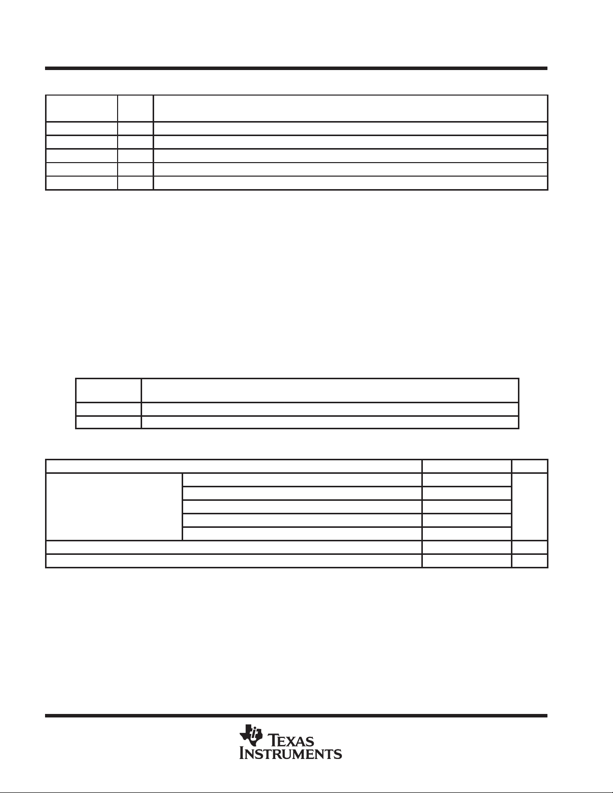
AVAILABLE OPTIONS
T
J
–40°C to 125°C
†
The DBVR passive indicates tape and reel of 3000 parts.
‡
The DBVT passive indicates tape and reel of 250 parts.
VOLTAGE PACKAGE PART NUMBER SYMBOL
3 V TPS76130DBVR†TPS76130DBVT
3.2 V
3.3 V
3.8 V
5 V TPS76150DBVR†TPS76150DBVT
SOT-23
TPS76132DBVR†TPS76132DBVT
TPS76133DBVR†TPS76133DBVT
TPS76138DBVR†TPS76138DBVT
‡
‡
‡
‡
‡
PAEI
PAFI
PAII
PAKI
PALI
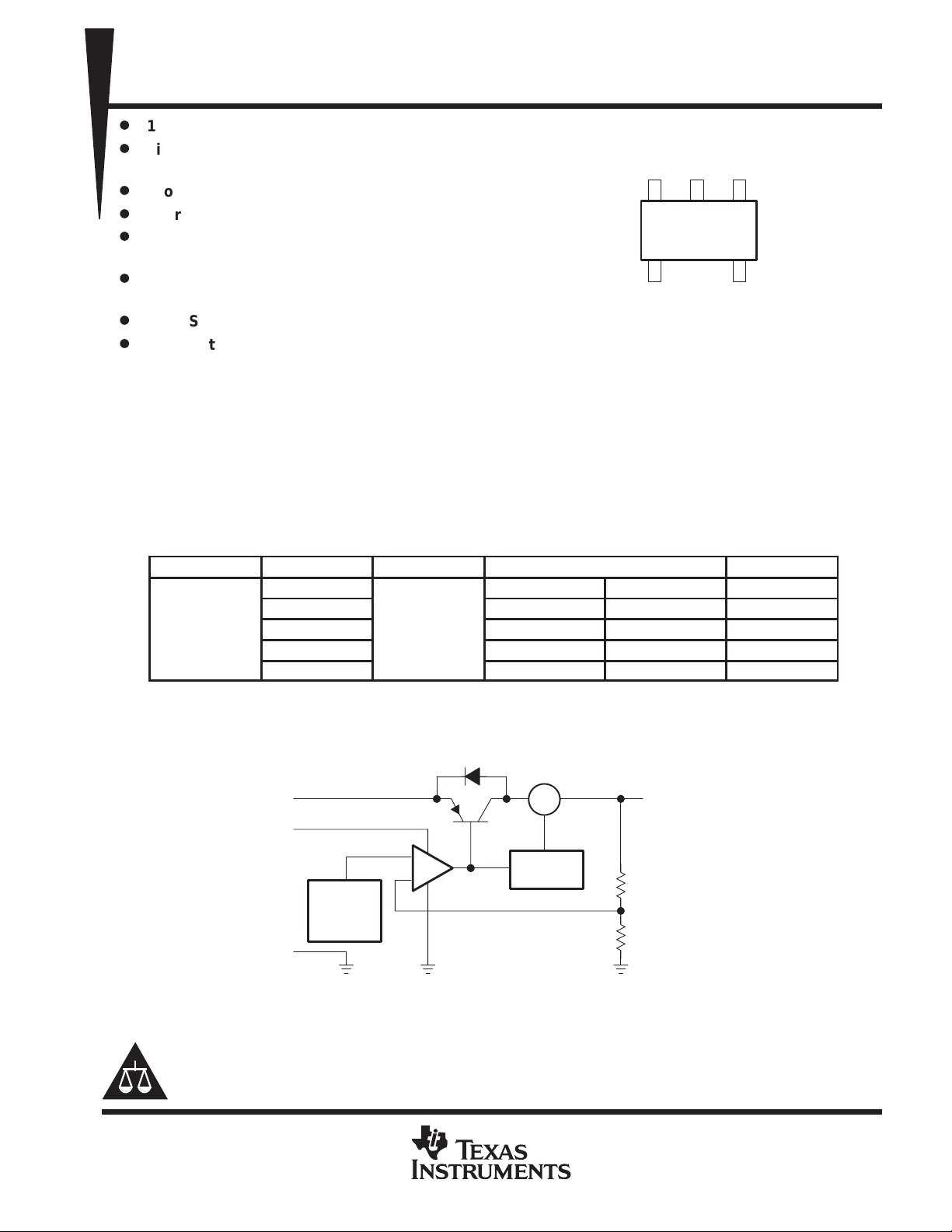
functional block diagram
IN
EN
V
ref
Thermal
Sense
GND
§
Current sense
Please be aware that an important notice concerning availability, standard warranty, and use in critical applications of
Texas Instruments semiconductor products and disclaimers thereto appears at the end of this data sheet.
PRODUCTION DATA information is current as of publication date.
Products conform to specifications per the terms of Texas Instruments
standard warranty. Production processing does not necessarily include
testing of all parameters.
CS
Current
Limit
+
POST OFFICE BOX 655303 • DALLAS, TEXAS 75265
§
OUT
Copyright 1999, Texas Instruments Incorporated
1
TPS76130, TPS76132, TPS76133, TPS76138, TPS76150
I/O
DESCRIPTION
LOW-POWER 100-mA LOW-DROPOUT LINEAR REGULATORS
SLVS178A – DECEMBER 1998 – REVISED FEBRUAR Y 1999
Terminal Functions
TERMINAL
NAME NO.
EN 3 I Enable input
GND 2 Ground
IN 1 I Input voltage
NC 4 No connection
OUT 5 O Regulated output voltage
absolute maximum ratings over operating free-air temperature range (unless otherwise noted)
Input voltage range, V
Voltage range at EN –0.3 V to V
Peak output current internally limited. . . . . . . . . . . . . . . . . . . . . . . . . . . . . . . . . . . . . . . . . . . . . . . . . . . . . . . . . . . . . . .
Continuous total dissipation See Dissipation Rating Table. . . . . . . . . . . . . . . . . . . . . . . . . . . . . . . . . . . . . . . . . . . .
Operating junction temperature range, T
Storage temperature range, T
ESD rating, HBM 1.5 kV. . . . . . . . . . . . . . . . . . . . . . . . . . . . . . . . . . . . . . . . . . . . . . . . . . . . . . . . . . . . . . . . . . . . . . . . .
†
Stresses beyond those listed under “absolute maximum ratings” may cause permanent damage to the device. These are stress ratings only, and
functional operation of the device at these or any other conditions beyond those indicated under “recommended operating conditions” is not
implied. Exposure to absolute-maximum-rated conditions for extended periods may affect device reliability.
NOTE 1: All voltages are with respect to device GND pin.
Recommended DBV 350 mW 3.5 mW/°C 192 mW 140 mW
Maximum DBV 437 mW 3.5 mW/° C 280 mW 227 mW
(see Note 1) –0.3 V to 16 V. . . . . . . . . . . . . . . . . . . . . . . . . . . . . . . . . . . . . . . . . . . . . . . . . . . . . . .
I
–40°C to 150°C. . . . . . . . . . . . . . . . . . . . . . . . . . . . . . . . . . . . . . . . . . .
J
stg
DISSIPATION RATING TABLE
PACKAGE
TA ≤ 25°C
POWER RATING
DERATING FACTOR
ABOVE TA = 25°C
TA = 70°C
POWER RATING
–65°C to 150°C. . . . . . . . . . . . . . . . . . . . . . . . . . . . . . . . . . . . . . . . . . . . . . . . . . . . . . . . .
TA = 85°C
POWER RATING
+ 0.3 V. . . . . . . . . . . . . . . . . . . . . . . . . . . . . . . . . . . . . . . . . . . . . . . . . . . . . . . . . . . . . . . . .
I
recommended operating conditions
MIN NOM MAX UNIT
TPS76130 3.35 16
TPS76132 3.58 16
Input voltage, V
Continuous output current, I
Operating junction temperature, T
I
O
TPS76133 3.68 16
TPS76138 4.18 16
TPS76150 5.38 16
0 100 mA
J
–40 125 °C
V
†
2
POST OFFICE BOX 655303 • DALLAS, TEXAS 75265
Quiescent current (GND current)
A
TPS76130, TPS76132, TPS76133, TPS76138, TPS76150
LOW-POWER 100-mA LOW-DROPOUT LINEAR REGULATORS
SLVS178A – DECEMBER 1998 – REVISED FEBRUAR Y 1999
electrical characteristics over recommended operating free-air temperature range,
V
= V
I
V
O
I
I(standby)
V
n
+ 1 V, IO = 1 mA, EN = VI, Co = 4.7 µF (unless otherwise noted)
O(typ)
PARAMETER TEST CONDITIONS MIN TYP MAX UNIT
TJ = 25°C 2.96 3 3.04
TPS76130
TPS76132
Output voltage TPS76133
TPS76138
TPS76150
Standby current EN = 0 V 1 µA
TPS76130 4 V < VI < 16, IO = 1 mA 3 10
TPS76132 4.2 V < VI < 16, IO = 1 mA 3 10
Input regulation
Output noise voltage BW = 300 Hz to 50 kHz Co = 10 µF, TJ = 25°C 190 µVrms
Ripple rejection f = 1 kHz, Co = 10 µF, TJ = 25°C 63 dB
TPS76133
TPS76138 4.8 V < VI < 16, IO = 1 mA 3 10
TPS76150 6 V < VI < 16 IO = 1 mA 3 10
TJ = 25°C, 1 mA < IO < 100 mA 2.9 3.04
1 mA < IO < 100 mA 2.89 3.07
TJ = 25°C 3.16 3.2 3.24
TJ = 25°C, 1 mA < IO < 100 mA 3.11 3.24
1 mA < IO < 100 mA 3.08 3.3
TJ = 25°C 3.26 3.3 3.34
TJ = 25°C, 1 mA < IO < 100 mA 3.21 3.34
1 mA < IO < 100 mA 3.18 3.4
TJ = 25°C 3.76 3.8 3.84
TJ = 25°C, 1 mA < IO < 100 mA 3.71 3.84
1 mA < IO < 100 mA 3.68 3.9
TJ = 25°C 4.95 5 5.05
TJ = 25°C, 1 mA < IO < 100 mA 4.88 5.05
1 mA < IO < 100 mA 4.86 5.1
IO = 0 mA, TJ = 25°C 90 115
IO = 0 mA 130
IO = 1 mA, TJ = 25°C 100 130
IO = 1 mA 170
IO = 10 mA, TJ = 25°C 190 220
IO = 10 mA 260
IO = 50 mA, TJ = 25°C 850 1100
IO = 50 mA 1200
IO = 100 mA, TJ = 25°C 2600 3600
IO = 100 mA 4000
4.3 V < VI < 16, IO = 1 mA 3 10
V
V
V
V
V
µ
mV
POST OFFICE BOX 655303 • DALLAS, TEXAS 75265
3
TPS76130, TPS76132, TPS76133, TPS76138, TPS76150
Dropout voltage
mV
IIInput current (EN)
A
VOOutput voltage
LOW-POWER 100-mA LOW-DROPOUT LINEAR REGULATORS
SLVS178A – DECEMBER 1998 – REVISED FEBRUAR Y 1999
electrical characteristics over recommended operating free-air temperature range,
V
= V
I
+ 1 V, IO = 1 mA, EN = VI, Co = 4.7 µF (unless otherwise noted) (continued)
O(typ)
PARAMETER TEST CONDITIONS MIN TYP MAX UNIT
IO = 0 mA, TJ = 25°C 1 3
IO = 0 mA 5
IO = 1 mA, TJ = 25°C 7 10
IO = 1 mA 15
p
Peak output current/current limit TJ = 25°C 100 150 mA
High level enable input 2 V
Low level enable input 0.8 V
p
IO = 10 mA, TJ = 25°C 40 60
IO = 10 mA 90
IO = 50 mA, TJ = 25°C 120 150
IO = 50 mA 180
IO = 100 mA, TJ = 25°C 170 240
IO = 100 mA 280
EN = 0 V –1 0 1
EN = V
I
2.5 5
µ
TYPICAL CHARACTERISTICS
Table of Graphs
FIGURE
p
Ground current vs Free-air temperature 7, 8, 9
Output noise vs Frequency 10
Z
o
V
DO
Output impedance vs Frequency 11
Dropout voltage vs Free-air temperature 12
Line transient response 13, 15
Load transient response 14, 16
vs Output current 1, 2, 3
vs Free-air temperature 4, 5, 6
4
POST OFFICE BOX 655303 • DALLAS, TEXAS 75265
 Loading...