

查询TPS7415供应商
TPS7415, TPS7418, TPS7425, TPS7430, TPS7433
FAST-TRANSIENT -RESPONSE USING SMALL OUTPUT CAPACITOR
200-mA LOW-DROPOUT VOLTAGE REGULATORS
SLVS212 – DECEMBER 1999
D
Fast Transient Response Using Small
Output Capacitor (10 µF)
D
200-mA Low-Dropout Voltage Regulator
D
Available in 1.5-V, 1.8-V, 2.5-V , 3-V and 3.3-V
D
Dropout Voltage Down to 170 mV at 200 mA
(TPS7433)
D
3% Tolerance Over Specified Conditions
D
8-Pin SOIC Package
D
Thermal Shutdown Protection
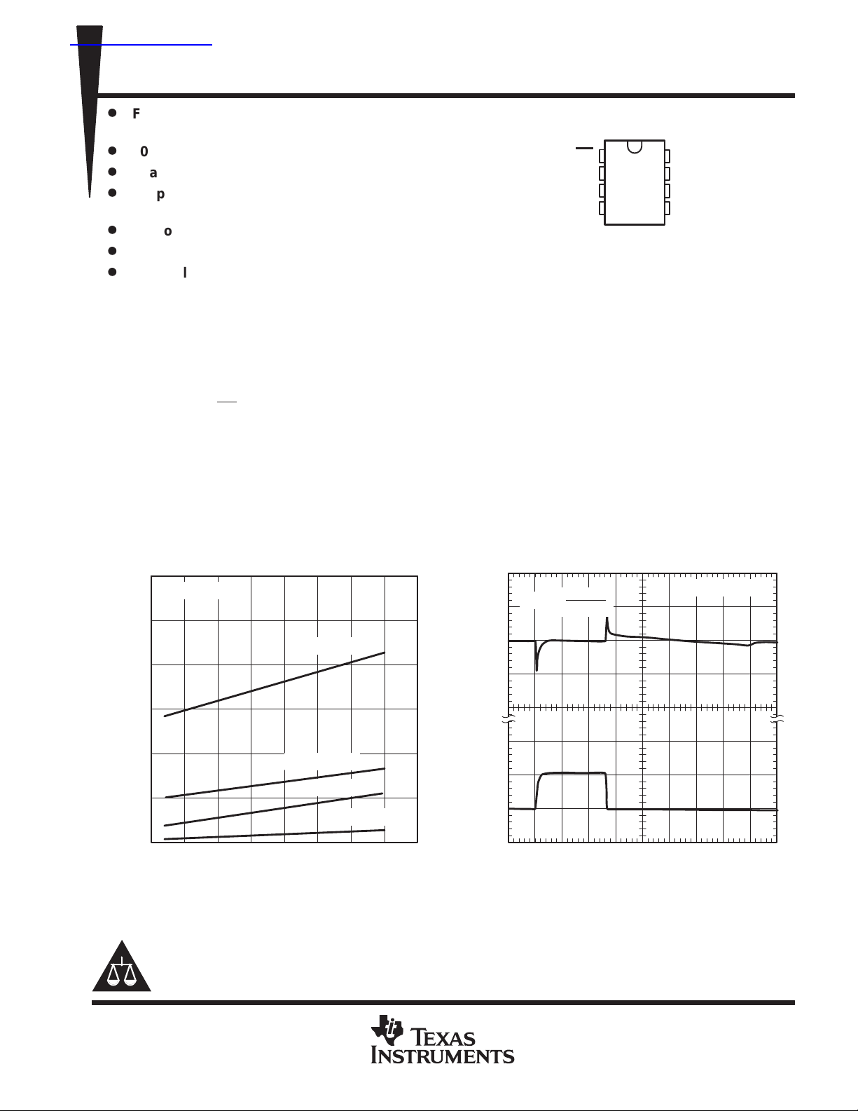
D PACKAGE
(TOP VIEW)
EN
1
NC
2
NC
3
4
IN
NC – No internal connection
8
7
6
5
SENSE
OUT
GND
IN
description
This device is designed to have a fast transient response and be stable with 1-µF capacitors. This combination
provides high performance at a reasonable cost.
Because the PMOS device behaves as a low-value resistor, the dropout voltage is very low (typically 170 mV
at an output current of 200-mA for the TPS7433). This LDO family also features a sleep mode; applying a TTL
high signal to EN (enable) shuts down the regulator, reducing the quiescent current to less than 1 µA at
TJ = 25°C.
The TPS74xx is offered in 1.5-V, 1.8-V, 2.5-V, 3-V, and 3.3-V. Output voltage tolerance is specified as a
maximum of 3% over line, load, and temperature ranges. The TPS74xx family is available in 8 pin SOIC
package.
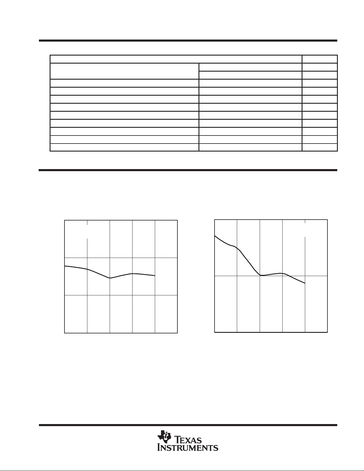
TPS7433
300
250
200
150
DROPOUT VOLTAGE
JUNCTION TEMPERATURE
VI = 3.2 V
vs
IO = 200 mA
100
50
0
– Change in
O
–50
V
∆
Output Voltage – mV
LOAD TRANSIENT RESPONSE
200 mA
di/dt =
25 µs
TPS7418
CO = 10 µF
100
– Dropout Voltage – mV
DO
V
50
0
–25 250 50 75 100 125 150
–50
TJ – Junction Temperature – °C
Please be aware that an important notice concerning availability, standard warranty, and use in critical applications of
Texas Instruments semiconductor products and disclaimers thereto appears at the end of this data sheet.
PRODUCTION DATA information is current as of publication date.
Products conform to specifications per the terms of Texas Instruments
standard warranty. Production processing does not necessarily include
testing of all parameters.
IO = 75 mA
IO = 50 mA
200
IO = 1 mA
POST OFFICE BOX 655303 • DALLAS, TEXAS 75265
0
O
I – Output Current – mA
0 300200100 400 500 700600 800 900 1000
t – Time – µs
Copyright 1999, Texas Instruments Incorporated
1
TPS7415, TPS7418, TPS7425, TPS7430, TPS7433
T
FAST-TRANSIENT -RESPONSE USING SMALL OUTPUT CAPACITOR
200-mA LOW-DROPOUT VOLTAGE REGULATORS
SLVS212 – DECEMBER 1999
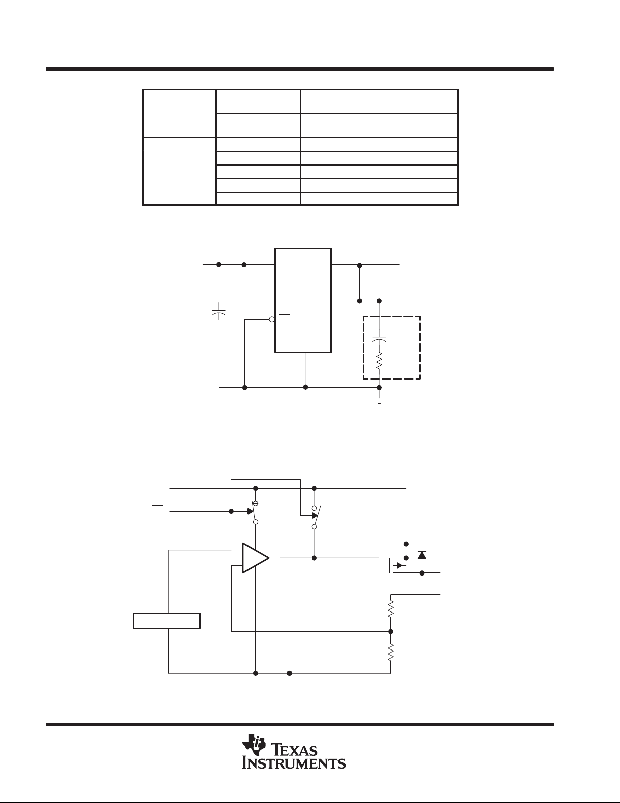
AVAILABLE OPTIONS
OUTPUT VOLTAGE
J
–40°C to 125°C
The D package is available taped and reeled. Add an R suffix to the device type (e.g.,
TPS7433DR).
V
I
1 µF
(V)
TYP
3.3 TPS7433D
3 TPS7430D
2.5 TPS7425D
1.8 TPS7418D
1.5 TPS7415D
TPS74xx
4
5
1
SENSE SENSE
IN
IN
EN
GND
PACKAGED DEVICES
8
7
OUT
6
SOIC
(D)
+
ESR
1 µF
V
C
O
O
†
functional block diagram
IN
EN
V
ref
†
See application information section for capacitor selection details.
Figure 1. Typical Application Configuration
_
+
GND
OUT
SENSE
R1
R2
2
POST OFFICE BOX 655303 • DALLAS, TEXAS 75265
I/O
DESCRIPTION
D
FAST-TRANSIENT -RESPONSE USING SMALL OUTPUT CAPACITOR
Terminal Functions
TERMINAL
NAME NO.
EN 1 I Enable input
GND 6 Regulator ground
IN 4, 5 I Input voltage
NC 2, 3 Not connected
OUT 7 O Regulated output voltage
SENSE 8 I Sense
TPS7415, TPS7418, TPS7425, TPS7430, TPS7433
200-mA LOW-DROPOUT VOLTAGE REGULATORS
SLVS212 – DECEMBER 1999
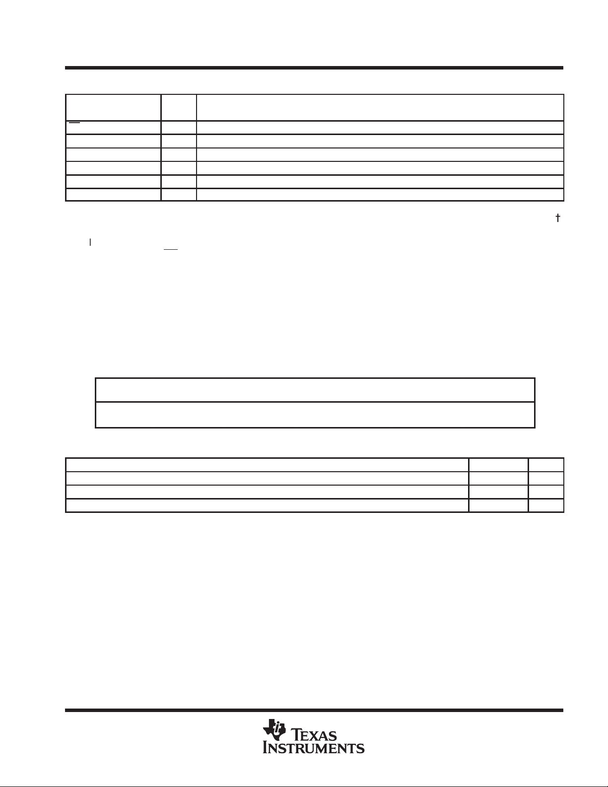
absolute maximum ratings over operating free-air temperature range (unless otherwise noted)
Input voltage range‡, VI –0.3 V to 8 V. . . . . . . . . . . . . . . . . . . . . . . . . . . . . . . . . . . . . . . . . . . . . . . . . . . . . . . . . . . . .
Voltage range at EN
–0.3 V to VI + 0.3 V. . . . . . . . . . . . . . . . . . . . . . . . . . . . . . . . . . . . . . . . . . . . . . . . . . . . . . . . . . .
Peak output current Internally limited. . . . . . . . . . . . . . . . . . . . . . . . . . . . . . . . . . . . . . . . . . . . . . . . . . . . . . . . . . . . . .
Continuous total power dissipation See dissipation rating tables. . . . . . . . . . . . . . . . . . . . . . . . . . . . . . . . . . . . . .
Operating virtual junction temperature range, TJ –40°C to 125°C. . . . . . . . . . . . . . . . . . . . . . . . . . . . . . . . . . . . .
Storage temperature range, T
†
Stresses beyond those listed under “absolute maximum ratings” may cause permanent damage to the device. These are stress ratings only, and
functional operation of the device at these or any other conditions beyond those indicated under “recommended operating conditions” is not
implied. Exposure to absolute-maximum-rated conditions for extended periods may affect device reliability.
‡
All voltage values are with respect to network terminal ground.
DISSIPATION RATING TABLE 1 – FREE-AIR TEMPERATURES
PACKAGE
AIR FLOW
(CFM)
0 568 mW 5.68 mW/°C 312 mW 227 mW
250 904 mW 9.04 mW/°C 497 mW 361 mW
–65°C to 150°C. . . . . . . . . . . . . . . . . . . . . . . . . . . . . . . . . . . . . . . . . . . . . . . . . . .
stg
TA < 25°C
POWER RATING
DERATING FACTOR
ABOVE TA = 25°C
TA = 70°C
POWER RATING
TA = 85°C
POWER RATING
recommended operating conditions
MIN MAX UNIT
Input voltage, V
Output current, IO (see Note 1) 0 200 mA
Operating virtual junction temperature, TJ (see Note 1) –40 125 °C
§
To calculate the minimum input voltage for your maximum output current, use the following equation: V
NOTE 1: Continuous current and operating junction temperature are limited by internal protection circuitry, but it is not recommended that the
§
I
I(min)
device operate under conditions beyond those specified in this table for extended periods of time.
= V
2.5 7 V
+ V
O(max)
DO(max load)
Ĕ
.
POST OFFICE BOX 655303 • DALLAS, TEXAS 75265
3
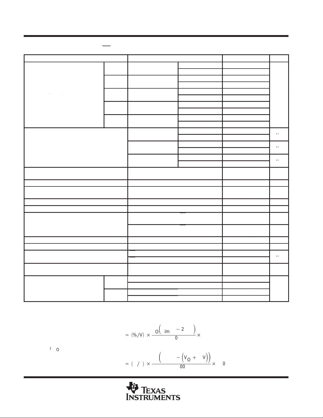
TPS7415, TPS7418, TPS7425, TPS7430, TPS7433
TPS7415
2.5 V
V
V
TPS7418
2.8 V
V
V
g( µ )
TPS7425
3.5 V
V
V
V
TPS7430
4.0 V
V
V
TPS7433
4.3 V
V
V
I
V
A
Quiescent current (GND current) (See Note 2)
I
100 mA
V
A
I
200 mA
V
A
Standby current
Input current (EN)
A
TPS7430
Dropout voltage (see Note 4)
mV
TPS7433
FAST-TRANSIENT -RESPONSE USING SMALL OUTPUT CAPACITOR
200-mA LOW-DROPOUT VOLTAGE REGULATORS
SLVS212 – DECEMBER 1999
electrical characteristics over recommended operating free-air temperature range,
V
= V
i
Output voltage (10 µA to 200 mA load)
(see Note 2)
Output voltage line regulation (∆VO/V
(see Notes 2 and 3)
Load regulation 5 mV
Output noise voltage
Output current Limit VO = 0 V 500 750 mA
Thermal shutdown junction temperature 150 °C
High level enable input voltage 2 V
Low level enable input voltage 0.7 V
p
Power supply ripple rejection (see Note 2)
p
NOTES: 2. Minimum IN operating voltage is 2.5 V or V
+ 1 V, I
O(typ)
PARAMETER TEST CONDITIONS TEST CONDITIONS MIN TYP MAX UNIT
3. If VO = 1.5 V then V
4. IN voltage equals VO(Typ) – 100 mV; TPS7430 and TPS7433 dropout limited by input voltage range limitations (i.e., TPS7430 input
voltage needs to drop to 2.9 V for purpose of this test).
= 1 mA, EN = 0 V, CO = 1 µF (unless otherwise noted)
O
TJ = 25°C 1.5
TJ = –40°C to 125°C 1.455 1.545
TJ = 25°C 1.8
TJ = –40°C to 125°C 1.746 1.854
TJ = 25°C 2.5
TJ = –40°C to 125°C 2.425 2.575
TJ = 25°C 3.0
TJ = –40°C to 125°C 2.910 3.090
TJ = 25°C 3.3
TJ = –40°C to 125°C 3.201 3.399
TJ = 25°C 80
TJ = –40°C to 125°C 115
TJ = 25°C 550
TJ = –40°C to 125°C 850
TJ = 25°C 1300
TJ = –40°C to 125°C 1500
CO = 1 µF,
EN = V
I,
EN = V
I,
CO = 1 µF,
imax
100
*
2.5 V
Ǔ
1000
O
)
= 7 V, V
imax
imin
Line Reg. (mV)
<
< 7
I
<
< 7
I
<
< 7
I
<
< 7
I
<
< 7
I
= 1 mA, EN = 0
O
=
O
=
O
VO + 1 V < VI ≤ 7 V, TJ = 25°C 0.06 %/V
BW = 300 Hz to 50 kHz,
TJ = 25°C
2.5 V < VI < 7 V,
TJ = 25°C
2.5 V < VI < 7 V,
TJ = –40°C to 125°C
EN = 0 V –1 1
EN = V
f = 100 Hz,
TJ = 25°C
IO = 200 mA, TJ = 25°C 180
IO = 200 mA, TJ = –40°C to 125°C 350
IO = 200 mA, TJ = 25°C 170
IO = 200 mA, TJ = –40°C to 125°C 315
O(typ)
= 2.5 V:
+ǒ%ńVǓ
, EN = 0
, EN = 0
I
+ 1 V, whichever is greater. Maximum IN voltage 7 V.
ǒ
V
V
O
190 µVrms
1 µA
3 µA
–1 1
55 dB
µ
µ
µ
µ
If VO ≥ 2.5 V then V
4
= 7 V, V
imax
imin
Line Reg. (mV)
POST OFFICE BOX 655303 • DALLAS, TEXAS 75265
= VO + 1 V:
+ǒ%ńVǓ
ǒ
V
imax
*ǒVO)
V
O
100
1V
Ǔ
Ǔ
1000
VOOutput voltage
TPS7415, TPS7418, TPS7425, TPS7430, TPS7433
FAST-TRANSIENT -RESPONSE USING SMALL OUTPUT CAPACITOR
200-mA LOW-DROPOUT VOLTAGE REGULATORS
SLVS212 – DECEMBER 1999
Table of Graphs
FIGURE
p
Ground current vs Junction temperature 7, 8
Power supply ripple rejection vs Frequency 12
Output noise vs Frequency 9
Z
o
V
DO
Output impedance vs Frequency 10
Dropout voltage vs Junction temperature 11
Line transient response 13, 15
Load transient response 14, 16
Output voltage vs Time 17
(Stability) Equivalent series resistance (ESR) vs Output current 19
TYPICAL CHARACTERISTICS
vs Output current 2, 3, 4
vs Junction temperature 5, 6
1.810
1.805
1.800
– Output Voltage – V
O
V
1.795
TPS7418
OUTPUT VOLTAGE
vs
OUTPUT CURRENT
VI = 2.8 V
TA = 25°C
0 200
50 100
IO – Output Current – mA
150 250
Figure 2
3.310
3.305
– Output Voltage – V
O
V
3.300
TPS7433
OUTPUT VOLTAGE
vs
OUTPUT CURRENT
VI = 4.3 V
TA = 25°C
0 200
50 100 150 250
IO – Output Current – mA
Figure 3
POST OFFICE BOX 655303 • DALLAS, TEXAS 75265
5

TPS7415, TPS7418, TPS7425, TPS7430, TPS7433
FAST-TRANSIENT -RESPONSE USING SMALL OUTPUT CAPACITOR
200-mA LOW-DROPOUT VOLTAGE REGULATORS
SLVS212 – DECEMBER 1999
TYPICAL CHARACTERISTICS
2.5
2.498
2.496
2.494
– Output Voltage – V
O
V
2.492
2.49
VI = 3.5 V
TA = 25°C
50 100
TPS7425
OUTPUT VOLTAGE
vs
OUTPUT CURRENT
150 2500 200
IO – Output Current – mA
Figure 4
1.820
1.818
1.816
1.814
1.812
1.810
1.808
– Output Voltage – V
O
V
1.806
1.804
1.802
–50
TPS7418
OUTPUT VOLTAGE
vs
JUNCTION TEMPERATURE
VI = 4.0 V
IO = 1 mA
IO = 50 mA
IO = 100 mA
IO = 200 mA
–25 250 50 75 100 125 150
TJ – Junction Temperature – °C
Figure 5
3.330
3.325
3.320
3.315
3.310
3.305
3.300
– Output Voltage – V
O
V
3.295
3.290
3.285
–50
TPS7433
OUTPUT VOLTAGE
vs
JUNCTION TEMPERATURE
VI = 4.3 V
IO = 1 mA
IO = 50 mA
IO = 100 mA
IO = 200 mA
–25 250 50 75 100 125 150
TJ – Junction Temperature – °C
Figure 6
JUNCTION TEMPERATURE
10000
1000
100
Ground Current – Aµ
VI = 2.8 V
10
1
–50 50
0 150
TJ – Junction Temperature – °C
TPS7418
GROUND CURRENT
vs
IO = 200 mA
IO = 100 mA
IO = 1 mA
100
Figure 7
6
POST OFFICE BOX 655303 • DALLAS, TEXAS 75265

TPS7415, TPS7418, TPS7425, TPS7430, TPS7433
FAST-TRANSIENT -RESPONSE USING SMALL OUTPUT CAPACITOR
200-mA LOW-DROPOUT VOLTAGE REGULATORS
SLVS212 – DECEMBER 1999
TYPICAL CHARACTERISTICS
JUNCTION TEMPERATURE
10000
1000
100
Ground Current – Aµ
VI =4.3 V
10
1
–50 50
TJ – Junction Temperature – °C
TPS7433
GROUND CURRENT
vs
IO = 200 mA
IO = 100 mA
IO = 1 mA
0
Figure 8
100
Ǹ
20µVHz
Ǹ
2µVHz
Ǹ
200nV Hz
Ǹ
20nV Hz
Output Spectral Noise Density
Ǹ
150
2nV Hz
250
OUTPUT SPECTRAL NOISE DENSITY
vs
FREQUENCY
VI = 4.3 V
CL = 1 µF
IO = 1 mA
IO = 200 mA
1k 10k 100k
f – Frequency – Hz
TA = 25°C
Figure 9
OUTPUT IMPEDANCE
FREQUENCY
100
VI = 4.3 V
CL = 1 µF
TA = 25°C
10
Ω
1
– Output Impedance –Z
o
0.1
0.01
0.01 10
0.1 1 1000
f – Frequency – kHz
Figure 10
vs
CL = 1 µF:
IO = 1 mA
CL = 1 µF
IO = 200 mA
100
250
200
150
100
– Dropout Voltage – mV
DO
V
50
0
TPS7430
DROPOUT VOLTAGE
JUNCTION TEMPERATURE
VI = 2.9 V
200 mA
100 mA
10 mA
10
TJ – Junction Temperature – °C
Figure 11
vs
110–40 60
POST OFFICE BOX 655303 • DALLAS, TEXAS 75265
7

TPS7415, TPS7418, TPS7425, TPS7430, TPS7433
FAST-TRANSIENT -RESPONSE USING SMALL OUTPUT CAPACITOR
200-mA LOW-DROPOUT VOLTAGE REGULATORS
SLVS212 – DECEMBER 1999
TYPICAL CHARACTERISTICS
RIPPLE REJECTION
vs
FREQUENCY
80
70
60
50
40
30
Ripple Rejection – dB
20
10
CL = 1 µF
IO = 100 mA
CL = 1 µF
IO = 200 mA
CL = 1 µF
IO = 1 mA
0
TPS7418
LINE TRANSIENT RESPONSE
200
0
– Change in
–200
O
V
∆
Output Voltage – mV
–300
3.8
2.8
– Input Voltage – V
I
V
CO = 1 µF
0 0.30.20.1 0.4 0.5 0.70.6 0.8 0.9 1
t – Time – ms
Figure 13
100 1k 10k10
f – Frequency – Hz
100k 1M 10M
Figure 12
TPS7418
LOAD TRANSIENT RESPONSE
100
200 mA
di/dt =
50
0
– Change in
O
–50
V
∆
Output Voltage – mV
200
0
O
I – Output Current – mA
0 0.30.20.1 0.4 0.5 0.70.6 0.8 0.9 1
25 µs
t – Time – ms
CO = 10 µF
Figure 14
8
POST OFFICE BOX 655303 • DALLAS, TEXAS 75265

TPS7415, TPS7418, TPS7425, TPS7430, TPS7433
FAST-TRANSIENT -RESPONSE USING SMALL OUTPUT CAPACITOR
200-mA LOW-DROPOUT VOLTAGE REGULATORS
SLVS212 – DECEMBER 1999
TYPICAL CHARACTERISTICS
200
0
– Change in
O
V
–200
∆
Output Voltage – mV
5.3
4.3
– Input Voltage – V
I
V
0 0.30.20.1 0.4 0.5 0.70.6 0.8 0.9 1
TPS7433
LINE TRANSIENT RESPONSE
CO = 1 µF
t – Time – ms
Figure 15
100
50
– Change in
O
V
–50
∆
Output Voltage – mV
–50
200
O
I – Output Current – mA
TPS7433
OUTPUT VOLTAGE
vs
TIME (AT STARTUP)
TPS7433
LOAD TRANSIENT RESPONSE
CO = 10 µF
0
0
0
0 0.30.20.1 0.4 0.5 0.70.6 0.8 0.9 1
t – Time – ms
di/dt =
200 mA
25 µs
Figure 16
VI = 7 V
4
2
0
– Output Voltage – V
O
V
5
0
Enable Pulse – V
0.60.40.2 0.8 1 1.41.2 1.6 1.8 20
t – Time – ms
Figure 17
POST OFFICE BOX 655303 • DALLAS, TEXAS 75265
9

TPS7415, TPS7418, TPS7425, TPS7430, TPS7433
FAST-TRANSIENT -RESPONSE USING SMALL OUTPUT CAPACITOR
200-mA LOW-DROPOUT VOLTAGE REGULATORS
SLVS212 – DECEMBER 1999
TYPICAL CHARACTERISTICS
+
C
ESR
To Load
O
R
L
V
I
IN
EN
OUT
GND
Figure 18. Test Circuit for Typical Regions of Stability (Figure 19)
TYPICAL REGIONS OF STABILITY
EQUIVALENT SERIES RESISTANCE (ESR)
vs
OUTPUT CURRENT
100
Ω
10
†
1
0.1
ESR – Equivalent Series Resistance –
0.01
0 50 100 150 200
Region of Instability
IO – Output Current – mA
Figure 19
†
ESR refers to the total series resistance, including the ESR of the capacitor, any series resistance added externally , and PWB trace resistance
to CO.
10
POST OFFICE BOX 655303 • DALLAS, TEXAS 75265

TPS7415, TPS7418, TPS7425, TPS7430, TPS7433
FAST-TRANSIENT -RESPONSE USING SMALL OUTPUT CAPACITOR
200-mA LOW-DROPOUT VOLTAGE REGULATORS
SLVS212 – DECEMBER 1999
APPLICATION INFORMATION
The TPS74xx family includes five voltage regulators (1.5 V, 1.8 V, 2.5 V, 3 V, and 3.3 V).
minimum load requirements
The TPS74xx family is stable even at zero load; no minimum load is required for operation.
SENSE terminal connection
The SENSE terminal must be connected to the regulator output for proper functioning of the regulator . Normally,
this connection should be as short as possible; however, the connection can be made near a critical circuit
(remote sense) to improve performance at that point. Internally, SENSE connects to a high-impedance
wide-bandwidth amplifier through a resistor-divider network and noise pickup feeds through to the regulator
output. Routing the SENSE connection to minimize/avoid noise pickup is essential. Adding an RC network
between SENSE and OUT to filter noise is not recommended because it can cause the regulator to oscillate.
external capacitor requirements
An input capacitor is not usually required; however, a ceramic bypass capacitor (1 µF or larger) improves load
transient response and noise rejection if the TPS74xx is located more than a few inches from the power supply .
A higher-capacitance electrolytic capacitor may be necessary if large (hundreds of milliamps) load transients
with fast rise times are anticipated.
Like all low dropout regulators, the TPS74xx requires an output capacitor connected between OUT and GND
to stabilize the internal control loop. The minimum recommended capacitance value is 1 µF and the ESR
(equivalent series resistance) must be at least 300 mΩ. Solid tantalum electrolytic and aluminum electrolytic
are all suitable, provided they meet the requirements described previously.
TPS74xx
V
I
1 µF
4
5
1
SENSE SENSE
IN
IN
EN
GND
OUT
6
8
7
+
ESR
1 µF
V
O
C
O
Figure 20. Typical Application Circuit
regulator protection
The TPS74xx PMOS-pass transistor has a built-in back diode that conducts reverse currents when the input
voltage drops below the output voltage (e.g., during power down). Current is conducted from the output to the
input and is not internally limited. When extended reverse voltage is anticipated, external limiting may be
appropriate.
POST OFFICE BOX 655303 • DALLAS, TEXAS 75265
11

TPS7415, TPS7418, TPS7425, TPS7430, TPS7433
FAST-TRANSIENT -RESPONSE USING SMALL OUTPUT CAPACITOR
200-mA LOW-DROPOUT VOLTAGE REGULATORS
SLVS212 – DECEMBER 1999
APPLICATION INFORMATION
regulator protection (continued)
The TPS74xx also features internal current limiting and thermal protection. During normal operation, the
TPS74xx limits output current to approximately 500 mA. When current limiting engages, the output voltage
scales back linearly until the overcurrent condition ends. While current limiting is designed to prevent gross
device failure, care should be taken not to exceed the power dissipation ratings of the package. If the
temperature of the device exceeds 150°C(typ), thermal-protection circuitry shuts it down. Once the device has
cooled below 130°C (typ), regulator operation resumes.
power dissipation and junction temperature
Specified regulator operation is assured to a junction temperature of 125°C; the maximum junction temperature
should be restricted to 125°C under normal operating conditions. This restriction limits the power dissipation
the regulator can handle in any given application. T o ensure the junction temperature is within acceptable limits,
calculate the maximum allowable dissipation, P
or equal to P
The maximum-power-dissipation limit is determined using the following equation:
D(max)
.
, and the actual dissipation, PD, which must be less than
D(max)
P
D(max)
Where
TJmax is the maximum allowable junction temperature.
R
is the thermal resistance junction-to-ambient for the package, i.e., 172°C/W for the 8-terminal
θJA
SOIC.
T
is the ambient temperature.
A
The regulator dissipation is calculated using:
PD+ǒVI*
Power dissipation resulting from quiescent current is negligible. Excessive power dissipation will trigger the
thermal protection circuit.
TJmax*T
+
R
V
O
Ǔ
A
q
JA
I
O
12
POST OFFICE BOX 655303 • DALLAS, TEXAS 75265

TPS7415, TPS7418, TPS7425, TPS7430, TPS7433
FAST-TRANSIENT -RESPONSE USING SMALL OUTPUT CAPACITOR
200-mA LOW-DROPOUT VOLTAGE REGULATORS
SLVS212 – DECEMBER 1999
MECHANICAL DATA
D (R-PDSO-G**) PLASTIC SMALL-OUTLINE PACKAGE
14 PIN SHOWN
14
1
0.069 (1,75) MAX
0.050 (1,27)
A
0.020 (0,51)
0.014 (0,35)
0.010 (0,25)
0.004 (0,10)
8
7
0.010 (0,25)
0.157 (4,00)
0.150 (3,81)
M
0.244 (6,20)
0.228 (5,80)
Seating Plane
0.004 (0,10)
PINS **
DIM
A MAX
A MIN
0.008 (0,20) NOM
Gage Plane
0°–8°
8
0.197
(5,00)
0.189
(4,80)
14
0.344
(8,75)
0.337
(8,55)
0.010 (0,25)
0.044 (1,12)
0.016 (0,40)
4040047/B 03/95
16
0.394
(10,00)
0.386
(9,80)
NOTES: A. All linear dimensions are in inches (millimeters).
B. This drawing is subject to change without notice.
C. Body dimensions do not include mold flash or protrusion, not to exceed 0.006 (0,15).
D. Four center pins are connected to die mount pad.
E. Falls within JEDEC MS-012
POST OFFICE BOX 655303 • DALLAS, TEXAS 75265
13

IMPORTANT NOTICE
T exas Instruments and its subsidiaries (TI) reserve the right to make changes to their products or to discontinue
any product or service without notice, and advise customers to obtain the latest version of relevant information
to verify, before placing orders, that information being relied on is current and complete. All products are sold
subject to the terms and conditions of sale supplied at the time of order acknowledgement, including those
pertaining to warranty, patent infringement, and limitation of liability.
TI warrants performance of its semiconductor products to the specifications applicable at the time of sale in
accordance with TI’s standard warranty. Testing and other quality control techniques are utilized to the extent
TI deems necessary to support this warranty . Specific testing of all parameters of each device is not necessarily
performed, except those mandated by government requirements.
CERTAIN APPLICATIONS USING SEMICONDUCTOR PRODUCTS MAY INVOL VE POTENTIAL RISKS OF
DEATH, PERSONAL INJURY, OR SEVERE PROPERTY OR ENVIRONMENTAL DAMAGE (“CRITICAL
APPLICATIONS”). TI SEMICONDUCTOR PRODUCTS ARE NOT DESIGNED, AUTHORIZED, OR
WARRANTED TO BE SUITABLE FOR USE IN LIFE-SUPPORT DEVICES OR SYSTEMS OR OTHER
CRITICAL APPLICA TIONS. INCLUSION OF TI PRODUCTS IN SUCH APPLICATIONS IS UNDERST OOD TO
BE FULLY AT THE CUSTOMER’S RISK.
In order to minimize risks associated with the customer’s applications, adequate design and operating
safeguards must be provided by the customer to minimize inherent or procedural hazards.
TI assumes no liability for applications assistance or customer product design. TI does not warrant or represent
that any license, either express or implied, is granted under any patent right, copyright, mask work right, or other
intellectual property right of TI covering or relating to any combination, machine, or process in which such
semiconductor products or services might be or are used. TI’s publication of information regarding any third
party’s products or services does not constitute TI’s approval, warranty or endorsement thereof.
Copyright 1999, Texas Instruments Incorporated
 Loading...